TAIWAN SEMICONDUCTOR TS1051 User Manual

TS1051
Constant Voltage and Constant Current Controller
For Battery Chargers and Adaptors
1/9 Version: B07
SOT-26
SOP-8
General Description
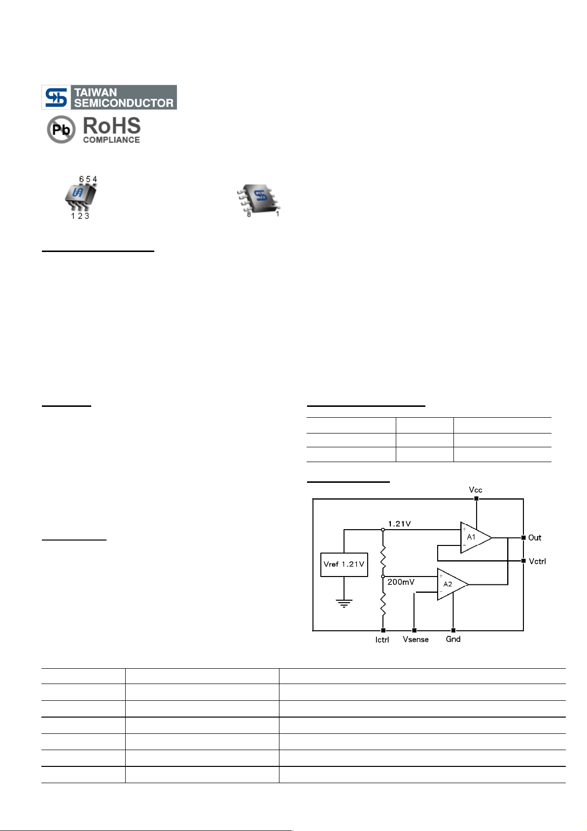
TS1051 is a highly integrated solution for SMPS applications requiring CV (constant voltage) and CC (constant current)
mode. TS1051 integrated one voltage reference, two operational amplifiers, and a current sensing circuit. The voltage
reference combined with one operational amplifier make it an ideal voltage controller, and the other low voltage
reference combined with the other operational amplifier make it an ideal current limiter for output low side current
sensing.
The current threshold is fixed, and precise. The only external components are:
* A resistor bridge to be connected to the output of the power supply (Adapter, battery charger) to set the voltage
regulation by dividing the desired output voltage to match the internal voltage reference value.
* A sense resistor having a value and allowable dissipation power which need to be chosen according to the internal
voltage threshold.
Ordering Information
Part No.
Package
Packing
TS1051CX6 RF
SOT-26
3Kpcs / 7” Reel
TS1051CS RL
SOP-8
2.5Kpcs / 13” Reel
Features
● Constant Voltage and Constant Current Control
● Low Voltage Operation
● Precision Internal Voltage Reference
● Low External Component Count
● Current Sink Output Stage
● Easy Compensation
● Low AC Mains Voltage Rejection
Application
● Battery Charger
● Adapters
Block Diagram
Pin Function Description
Name
Type
Function
V
CTRL
Analog Input
Input Pin of the Voltage Control Loop
VND
Power Supply
Ground Line. 0V Reference For All Voltage
Out
Current Sink Output
Output Pin. Sinking Current Only
I
CTRL
Analog Input
Input Pin of the Current Control Loop
V
SENSE
Analog Input
Input Pin of the Current Control Loop
VCC
Power Supply
Position Power Supply Line
Pin Definition:
1. V
CTRL
6. VCC
2. VND 5, V
SENSE
3. Out 4. I
CTRL
Pin Definition:
1. V
CTRL
8. VND
2. VCC 7, Out
3. V
SENSE
6. I
CTRL
4. N.C 5. N.C

TS1051
Constant Voltage and Constant Current Controller
For Battery Chargers and Adaptors
2/9 Version: B07
Absolute Maximum Rating
Parameter
Symbol
Value
Unit
DC Supply Voltage
VCC
14
V
Input Voltage
VIN
-0.3 to VCC
V
Operating Temperature
TOP
0 to +85
o
C
Maximum Junction Temperature Range
TJ
150 oC
SOP-8
130 oC/W
Thermal Resistance Junction to Ambient
SOT-26
Rθja
250 oC/W
Operating Condition
Parameter
Symbol
Value
Unit
DC Supply Voltage
VCC
2.5 to 12
V
Electrical Specifications (Ta=25
o
C, VIN=5V unless otherwise noted)
Note:
1: If the Voltage on Vctrl (the negative input of the amplifier) is higher than the positive amplifier input (Vref-1.21V), and
it is increased by 1mV, the sinking current at the output will be increased by 3.5mA.
2: The internal Voltage reference is set at 1.21V (bandgap reference). The voltage control loop precision takes into
account the cumulative effects of the internal voltage reference deviation as well as the input offset voltage of the
trans-conductance operational amplifier. The internal voltage reference is fixed by bandgap, and trimmed to 0.5%
accuracy at room temperature.
3: When the positive input at Ictrl is lower than -200mV, and the voltage is decreased by 1mV, the sinking current
at the output will be increased by 7mA
4: The internal current sense threshold is set to -200mV. The current control loop precision takes into account the
cumulative effects of the internal voltage reference deviation as well as the input offset voltage of the
trans-conduction operational amplifier
Parameter
Symbol
Min
Typ
Max
Unit
Total Current Consumption
Total Supply Current – not taking the output sinking current into
account
ICC
--
1.1 2 mA
Voltage Control Loop
Trans-conduction Gain (Vctrl) sink Current Only (Note 1)
GMW
1
3.5
--
mA/mV
Voltage Control Loop Reference (Note 2)
V
REF
1.198
1.21
1.222
V
Input Bias Current (Vctrl)
I
IBV
--
50
--
nA
Current Control Loop
Trans-conduction Gain (Ictrl) sink Current only (Note 3)
GMI
1.5 7 --
mA/mV
Current Control Loop Reference, (Note 4) I
OUT
=2.5A,
V
SENSE
196
200
204
mV
Current Out of Pin Ictrl at – 200mV
I
IBI
--
25
--
µA
Output Stage
Low Output Voltage at 10mA sinking Current
VOL
--
200
--
mV
Output Short Circuit Current. Output to V
CC.
Sink Current Only
IOS
--
27
50
mA

TS1051
Constant Voltage and Constant Current Controller
For Battery Chargers and Adaptors
3/9 Version: B07
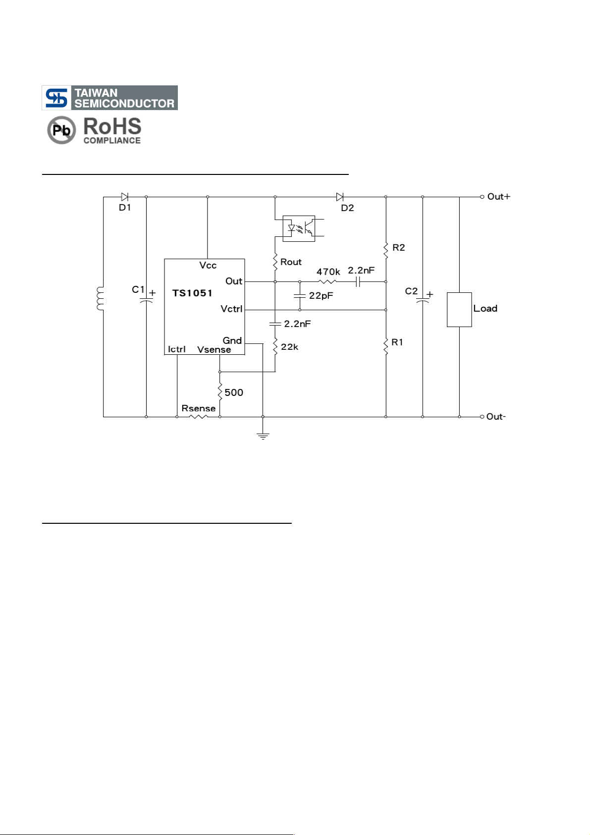
Typical Adapter or Battery Charger Application Circuit
* In the above application schematic, the TS1051 is used on the secondary side of a fly-back adapter (or battery
charger) to provide an accurate control of voltage and current. The above feedback loop is made with an optocoupler.
Principle of Operation and Application Hints
Voltage Control
The voltage loop is controlled via a first trans-conductance operational amplifier, the resistor bridge R1, R2, and the
optocoupler which is directly connected to the output.
The relation between the values of R1 & R2 should be chosen as following:
*R1=R2 x Vref / (Vout-Vref)
Where Vout is the desired output voltage.
To Avoid the discharge of the load, the resistor bridge R1 & R2 should be highly resistive. For this type of application, a
total value of 100KΩ (or more) would be appropriate for the resistors R1 & R2. As an example, with R2=100KΩ,
Vout=4.10V, Vref=1.21V, then R1=41.9KΩ.
Note that if the low drop diode should be inserted between the load and the voltage regulation resistor bridge to avoid
current flowing from the load through the resistor bridge, this drop should be taken into account into the above
calculations by replacing Vout by (Vout + Vdrop).
 Loading...