

TE
tm
SDRAM
FEATURES
• 3.3V power supply
Clock cycle time : 6 / 7 / 8 / 10 ns
•
Dual banks operation
•
• LVTTL compatible with multiplexed address
• All inputs are sampled at the positive going
edge of system clock
Burst Read Single-bit Write operation
•
• DQM for masking
• Auto refresh and self refresh
32ms refresh period (2K cycle)
•
• MRS cycle with address key programs
- CAS Latency ( 2 & 3 )
- Burst Length ( 1 , 2 , 4 , 8 & full page)
- Burst Type (Sequential & Interleave)
• Available package type in 50 pin TSOP(II)
and 60-pin CSP.
Operating temperature :
•
- -5 ~ +70 °C
-
PART NUMBER EXAMPLES
CH
-40 ~ +85 °C
T431616A
1M x 16 SDRAM
512K x 16bit x 2Banks Synchronous DRAM
GRNERAL DESCRIPTION
The T431616A is 16,777,216 bits synchronous
high data rate Dynamic RAM organized as
2 x 524,288 words by 16 bits , fabricated with high
performance CMOS technology . Synchronous
design allows precise cycle control with the use of
system clock I/O transactions are possible on every
clock cycle . Range of operating frequencies ,
programmable burst length and programmable
latencies allow the same device to be useful for a
variety of high bandwidth , high performance
memory system applications.
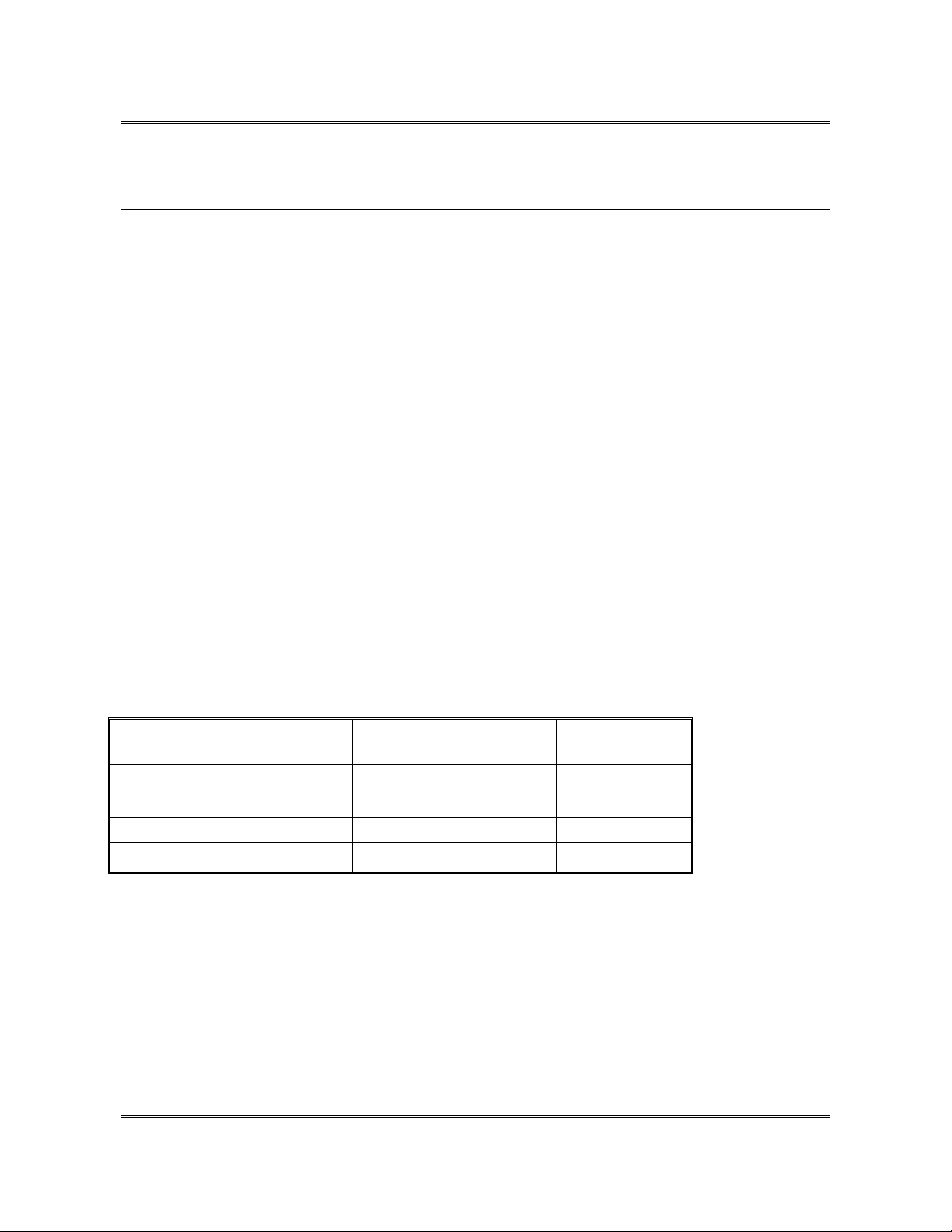
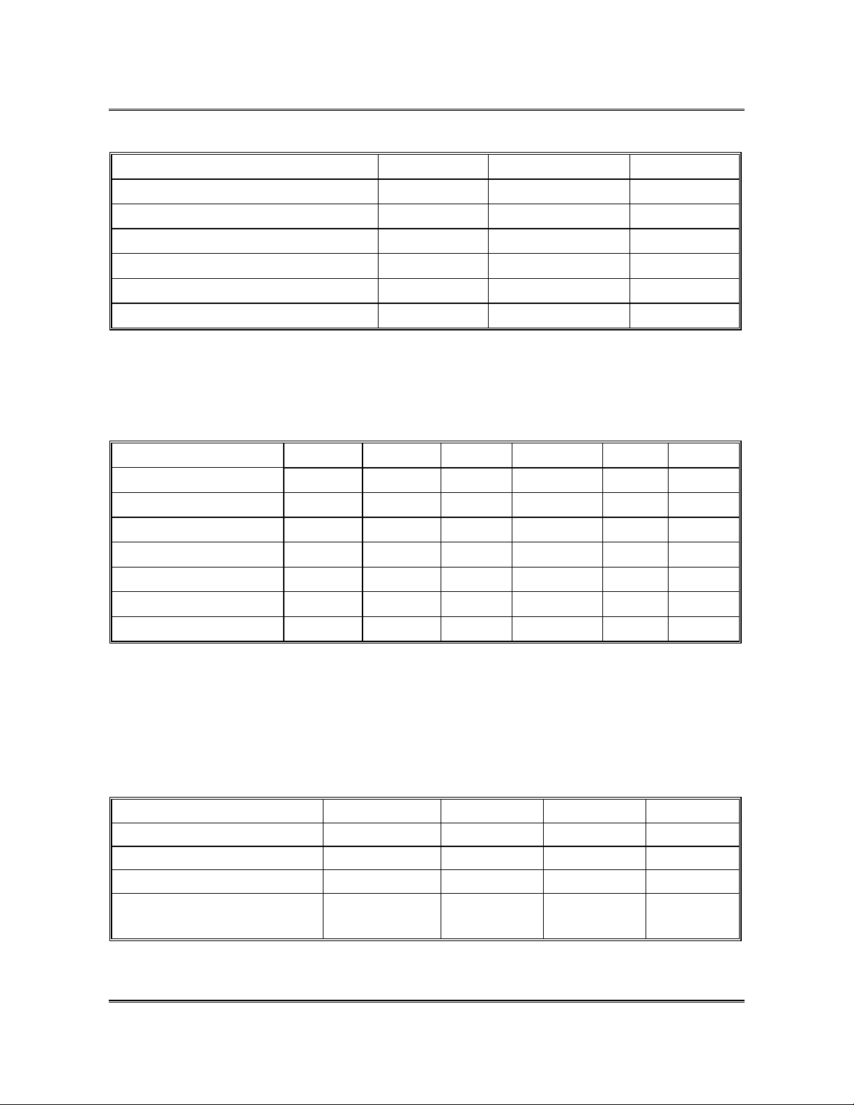
PART NO.
T431616A-7S
T431616A-7C
T431616A-7SI
T431616A-7CI
Taiwan Memory Technology, Inc. reserves the right P. 1
to change products or specifications without notice. Revision: C
CLOCK
CYCLE TIME
7ns
7ns
7ns
7ns
MAX
FREQUENCY
143 MHz
143 MHz
143 MHz
143 MHz
PACKAGE
TSOP-II
CSP
TSOP-II
CSP
OPERATING
TEMPERATURE
-5 ~ +70 °C
-5 ~ +70 °C
-40 ~ +85 °C
-40 ~ +85 °C
Publication Date: DEC. 2000
TE
tm
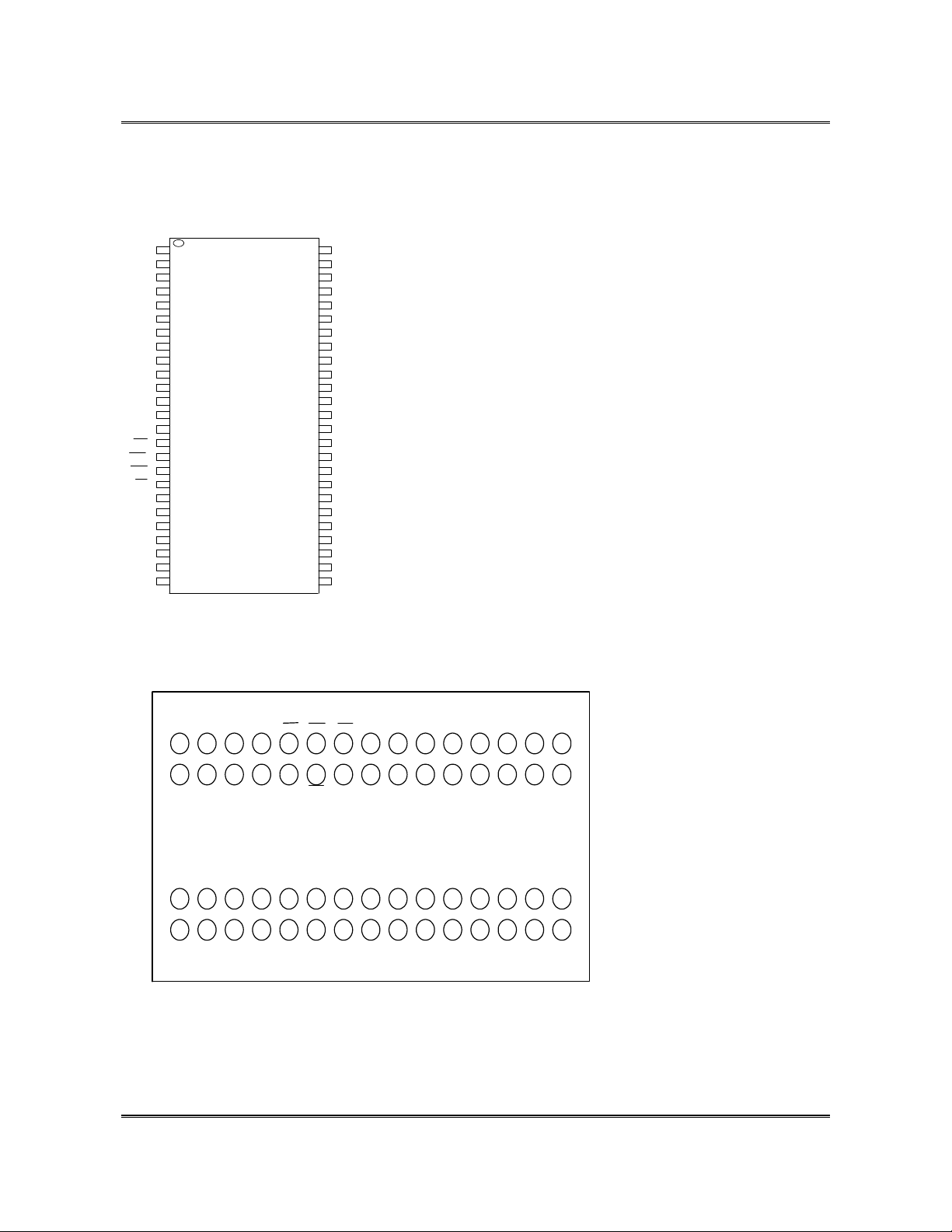
PIN ARRANGEMENT
(TSOP-II
DD
V
DQ0
DQ1
SSQ
V
DQ2
DQ3
V
DDQ
DQ4
DQ5
V
SSQ
DQ6
DQ7
DDQ
V
LDQM
WE
CAS
RAS
CS
BA
A10/AP
A0
A1
A2
A3
V
DD
(CSP Bottom View)
CH
1
2
3
4
5
6
7
8
9
10
11
12
13
14
15
16
17
18
19
20
21
22
23
24
25
Top View)
50
49
48
47
46
45
44
43
42
41
40
39
38
37
36
35
34
33
32
31
30
29
28
27
26
Vss
DQ15
DQ14
SSQ
V
DQ13
DQ12
V
DDQ
DQ11
DQ10
V
SSQ
DQ9
DQ8
V
DDQ
N.C/RFU
UDQM
CLK
CKE
N.C
A9
A8
A7
A6
A5
A4
50PINTSOP(II)
(400mil x 825mil)
Vss
(0.8 mm PIN PITCH)
T431616A
CAS
VDD A1 A10/AP N.C
CS
WE
N.C
DQ5DQ6DQ7
VDDDQ1DQ2DQ3
7
6
N.C N.CA0A2A3
RAS
LDQM
N.C N.C
VSSQ
VDDQ
DQ4
DQ0VDDQVSSQ
5
4
3
A4 A5A6A7A8A9
N.C
CLK
UDQM
N.C N.C
VDDQ
DQ11
VDDQ
VSSQVSSQ
DQ15
2
1
BAVSS
CKE
RPNML
N.C N.C N.C
DQ8
JHG EFKABCD
DQ10DQ9
DQ13DQ12
DQ14 VSS
Taiwan Memory Technology, Inc. reserves the right P. 2
to change products or specifications without notice. Revision: C
Publication Date: DEC. 2000
TE
tm
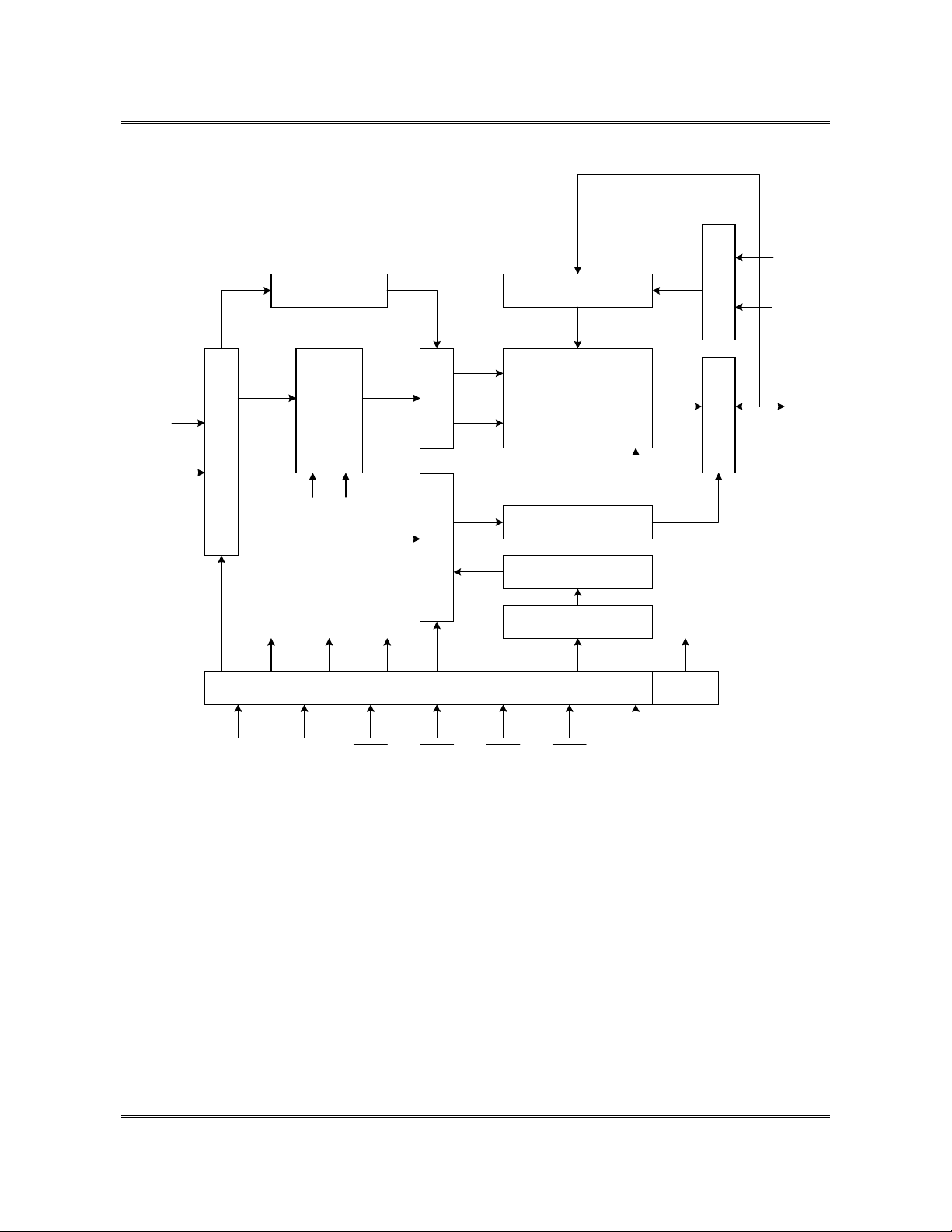
BLOCK DIAGRAM
CH
T431616A
CLK
ADD
LCKE
I/O Control Output Buffer
Bank Select
Refresh Counter
Row Buffeer
Address Register
LCBR
LRAS
LWELCBRLRAS
Timing Register
Row Decoder
Col. Buffer
Data Input Register
Sense AMP
512K x 16
512K x 16
Column Decoder
Latency & B urst L ength
Programming Register
LWCBRLCAS
LDQM
LWE
LDQM
DQi
CAS WE
Taiwan Memory Technology, Inc. reserves the right P. 3
L(U)DQMRASCSCKECLK
Publication Date: DEC. 2000
to change products or specifications without notice. Revision: C
TE
tm
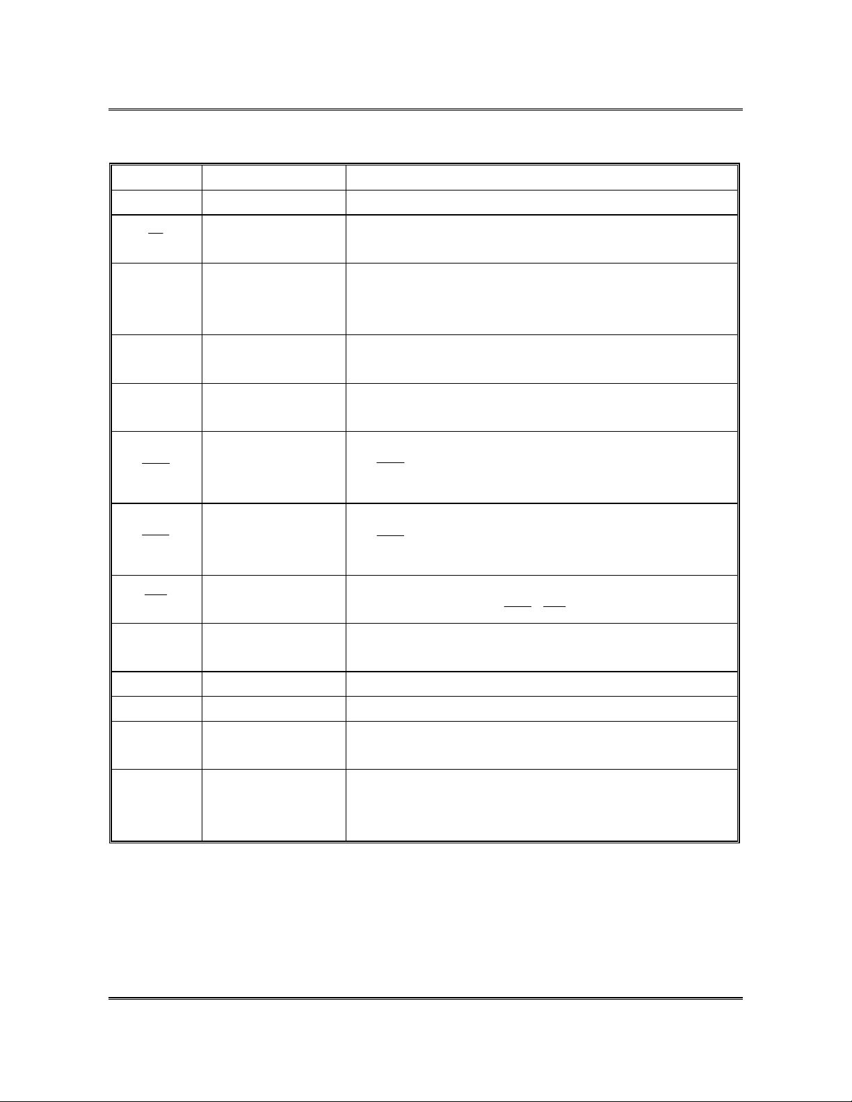
PIN DESCRIPTION
CH
T431616A
PIN NAME
CLK System Clock
CS
CKE Clock Enable
A0 ~ A10/AP Address
BA Bank Select Address
RAS
CAS
Chip Select
Row Address Strobe
Column Address Strobe
INPUT FUNCTION
Active on the positive going edge to sample all input.
Disables or enables device operation by masking or enabling all input
except CLK,CKE and L(U)DQM
Masks system clock to freeze operation from the next clock cycle.
CKE should be enabled at least one cycle prior to new command.
Disable input buffers for power down in standby.
Row/column addresses are multiplexed on the same pins.
Row address : RA0 ~ RA10,column address : CA0 ~ CA7
Selects bank to be activated during row address latch time.
Select bank for read/write during column address latch time.
Latches row addresses on the positive going edge of the CLK
RAS
CAS
low.
low.
with
Enables row access & precharge.
Latches column addresses on the positive going edge of the CLK
with
Enables column access .
WE
L(U)DQM
DQ0 ~ DQ15 Data Input/Output
VDD/VSS Power Supply/Ground
V
DDQ/VSSQ
N.C/RFU
Write Enable
Data Input/Output
Mask
Data Output
Power/Ground
No
Connection/Reserved
for Future Use
Enables write operation and row precharge.
Latches data in starting from
Makes data output Hi-Z, t
Blocks data input when L(U)DQM active.
Data inputs/outputs are multiplexed on the same pins.
Power and ground for the input buffers and the core logic.
Isolated power supply and ground for the output buffers to provide
improved noise immunity.
This pin is recommended to be left No Connection on the device.
CAS, WE
after the clock and masks the output.
SHZ
active.
Taiwan Memory Technology, Inc. reserves the right P. 4
to change products or specifications without notice. Revision: C
Publication Date: DEC. 2000
TE
tm
ABSOLUTE MAXIMUM RATINGS
Parameter Symbol Value Unit
CH
T431616A
Voltage on Any Pin Relative To Vss VIN,V
Supply Voltage Relative To Vss VDD,V
Short circuit Output Current I
Power Dissipation PD 1 W
Operating Temperature T
Storage Temperature T
Permanent device damage may occur if ABSOLUTE MAXIMUM RATINGS are exceeded.
Note :
Functional operation should be restricted to recommended operating condition.
Exposure to higher than recommended voltage for extended periods of time could affect device reliability.
RECOMMENDED DC OPERATING CONDITIONS
-1.0 to 4.6 V
OUT
-1.0 to 4.6 V
DDQ
50 mA
out
-5 to +70 / -40 to +85 °C
OPR
-55 to +125 °C
stg
(TA = -5 to +70 °C / -40 to +85 °C , Voltage referenced to VSS=0V)
Parameter Symbol Min. Typ Max. Unit Notes
Supply Voltage VDD,V
Input High Voltage VIH 2.0 3.0 VDD+0.3V V 1
Input Low Voltage VIL -0.3 0 0.8 V 2
Output logic high voltage VOH 2.4 - - V IOH=-2mA
Output logic low voltage VOL - - 0.4 V IOL=2mA
3.0 3.3 3.6 V
DDQ
Input leakage current IIL -5 - 5 uA 3
Output leakage current IOL -5 - 5 uA 4
1. V
Note :
4. Dout = disable, 0V≤ V
(max) = 4.6V AC for pulse width ≤ 10ns acceptable.
IH
2. VIL (min) = -1.0V AC for pulse width ≤ 10ns acceptable.
3. Any input 0V≤ VIN ≤ VDD+ 0.3V , all other pin are not under test = 0V.
V
OUT
≤
DD .
CAPACITANCE
=25 °C,VDD=3.3V, f = 1MHz)
(T
A
CLOCK C
ADDRESS C
DQ0 ~ DQ15 C
RAS,CAS,WE,CS,CKE,LDQM,
UDQM
Pin Symbol Min Max Unit
2.5 4.0 pF
CLK
2.5 5.0 pF
ADD
4.0 6.5 pF
OUT
CIN 2.5 5.0 pF
Taiwan Memory Technology, Inc. reserves the right P. 5
to change products or specifications without notice. Revision: C
Publication Date: DEC. 2000
TE
tm
DC CHARACTERISTICS
TA = -5 to 70°C / -40 to +85 °C , VIH(min)/VIL(max)=2.0V/0.8V
CH
T431616A
Parameter Symbol
Operating Current
( One Bank Active)
Precharge Standby
I
I
CC1
CC2
Current in power-
I
down mode
CC2
Precharge Standby
I
Current in non
CC2
power-down mode
I
CC2
Active Standby
I
CC3
Current in power-
I
down mode
CC3
Active Standby
I
Current in non
CC3
power-down mode
I
(One Bank Active)
CC3
Operating Current
I
I
CC4
CC5
(Burst Mode)
Refresh Current
Speed version
Unit Test Condition
-6 -7 -8 -10
160 150 140 120 mA
P 2
Burst Length = 1
t
CKE≤ VIL(max),
mA
PS 2
CKE≤ VIL(max),CLK ≤VIL(max),
CKE
N 30
Input signals are changed one time during 30ns
mA
CKE≥VIH(min),CLK≤VIL(min),
NS 2
Input signals are stable
P 10
CKE≤ VIL(max),
mA
PS 10
CKE≤ VIL(max),CLK ≤VIL(max),
CKE≥VIH(min),
N 40
Input signals are changed one time during 30ns
mA
CKE≥VIH(min),CLK≤VIL(min),
NS 10
Input signals are stable
180 170 160 140
180 170 160 140
180 170 160 140 mA
CAS Latency 3
mA
CAS Latency 2
t
RC
RC
t
≥
RC
≥
t
≥
RC
(min) ,
VIH(min),
(min)
t
t
≥
(min),IOL= 0 mA
CC
CC
t
=15ns
CC
≥
VIH(min),
CS
t
=15ns
CC
≥
VIH(min),
CS
=0 mA,Page Burst
I
OL
All Band Activated
t
t
=
CCD
CCD
t
t
CC
t
CC
t
CC
(min)
t
CC
=15ns
CC
=•
t
CC
=15ns
=•
Note
1,3
3
=•
3
3
=•
3
1,3
2,3
Self refresh
Current
1 mA
I
CC6
Note: 1. Measured with output open. Addresses are changed only one time during
2. Refresh period is 32ms. Addresses are changed only one time during
t
3.
: Clock cycle time.
CC
t
: Row cycle time.
RC
t
: Column address to column address delay time.
CCD
CKE≤0.2V
t
CC
t
CC
(min)
(min)
.
.
Taiwan Memory Technology, Inc. reserves the right P. 6
to change products or specifications without notice. Revision: C
Publication Date: DEC. 2000
TE
tm
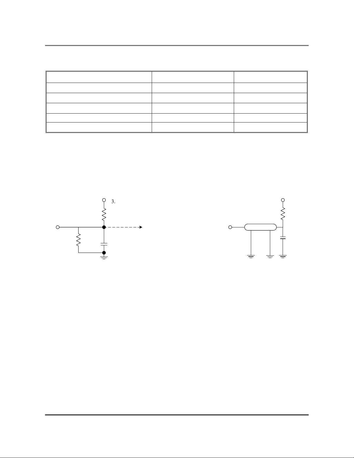
AC OPERATING CONDITIONS
(VDD=3.3V ±0.3V ,TA= -5 to 70°C /-40 to +85°C )
Input levels (VIH/VIL) 3.0 / 0 V
Input timing measurement reference level 1.4 V
CH
Parameter Value Unit
T431616A
Input rise and fall time
Output timing measurement reference level 1.4 V
Output load condition See Fig.2
t
r / tf = 1 / 1
ns
Vtt=1.4v
50 ohm
30pf
Output
870 ohm
3.3V
1200 ohm
30pf
ZO=50 ohmOutput
VOH(DC)=2.4,IOH=-2mA
VOL(DC)=0.4,IOL=2mA
(Fig.1) DC Output Load Circuit (Fig.2)AC Output Load Circuit
Taiwan Memory Technology, Inc. reserves the right P. 7
to change products or specifications without notice. Revision: C
Publication Date: DEC. 2000
TE
tm
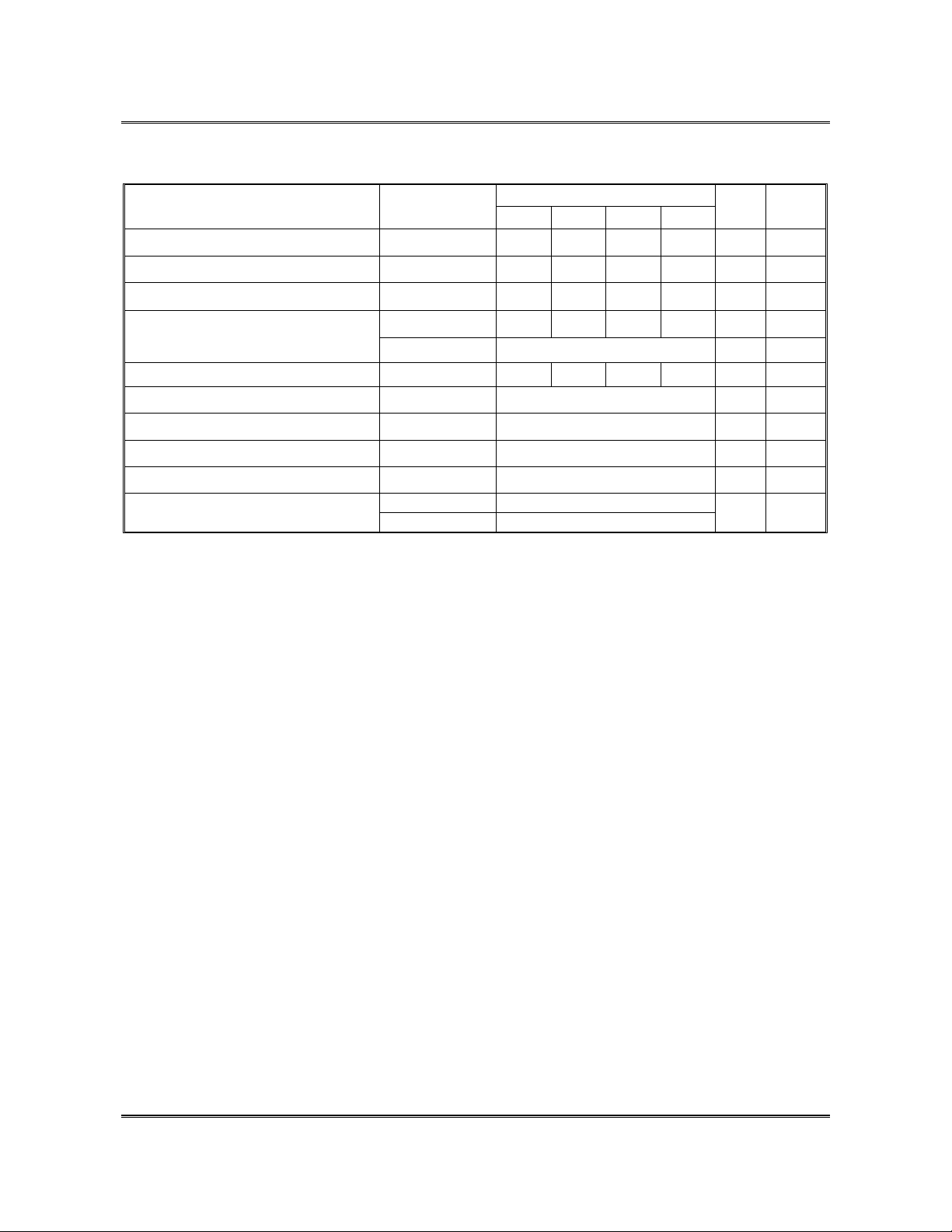
OPERATING AC PARAMETER
(AC opterating conditions unless otherwise noted)
Row active to row active delay
RAS to CAS delay
Row precharge time
Row active time
Row cycle time
Last data in to new col. Address delay
Last data in to row precharge
Last data in to burst stop
Col. Address to col. Address delay
Number of valid output data
Note:
with clock cycle time and then rounding off to the next higher integer.
2. Minimum delay is required to complete write.
3. All parts allow every cycle column address change.
4. In case of row precharge interrupt, auto precharge and read burst stop.
The earliest a precharge command can be issued after a Read command without the loss of data is
CL + BL-2 clocks.
CH
Parameter Symbol
t
(min)
RRD
t
(min)
RCD
t
(min)
RP
t
(min)
RAS
t
RAS
t
RC
t
CDL
t
RDL
t
BDL
t
CCD
CAS latency=3 1
CAS latency=2 1
1. The minimum number of clock cycles is determined by dividing the minimum time required
(max)
(min)
(min)
(min)
(min)
(min)
Speed Version
-6 -7 -8 -10
12 14 16 20 ns 1
16 16 20 20 ns 1
18 20 20 20 ns 1
42 42 48 50 ns 1
100K ns
60 63 68 70 ns 1
1 CLK 2
2 CLK 2
1 CLK 2
1 CLK 3
T431616A
Unit Note
ea 4
Taiwan Memory Technology, Inc. reserves the right P. 8
to change products or specifications without notice. Revision: C
Publication Date: DEC. 2000
TE
tm
AC CHARACTERISTICS
(AC opterating conditions unless otherwise noted)
CLK cycle time
CH
-6 -7 -8 -10
Parameter
CAS Latency = 3 6 7 8 10
CAS Latency = 2
Symbol
Min Max Min Max Min Max Min Max
t
CC
8
1K
8.6
1K
10
1K
T431616A
1K ns 1
10
Unit Note
CLK to valid
Output delay
Output data hold time
CLK high pulse width
CLK low pulse width
Input setup time
Input hold time
CLK to output in Low-Z
CLK to output in
Hi-Z
CAS Latency = 3 - 5.5 - 6 - 6 - 7 ns
t
SAC
CAS Latency = 2
t
OH
t
CH
t
CL
t
SS
t
SH
t
SLZ
CAS Latency = 3 - 5.5 - 6 - 6 - 7 ns
t
SHZ
CAS Latency = 2
- 6 - 6 - 7 - 9 ns
2 2.5 2.5 2.5 ns 2
2 2.5 3 3 ns 3
2 2.5 3 3 ns 3
1.5 1.75 2 2.5 ns 3
1 1 1 1 ns 3
1 1 1 1 ns 2
- 6 - 6 - 7 - 9 ns
Note:
1. Parameters depend on programmed CAS latency.
2. If clock rising time is longer than 1ns,(tr/2-0.5)ns should be added to the parameter.
3. Assumed input rise and fall time (tr & tf)=1ns.
If tr & tf is longer than 1ns,transient time compensation should be considered,
i.e.,[(tr+tf)/2-1]ns should be added to the parameter.
1
Taiwan Memory Technology, Inc. reserves the right P.9
to change products or specifications without notice. Revision: C
Publication Date: DEC. 2000
TE
tm
FREQUENCY vs. AC PARAMETER RELATIONAHIP TABLE
T431616A-6S (Unit : number of clock)
Frequency
166MHz(6.0ns)
143MHz(7.0ns) 3 9 6 3 2 3 1 1 2
125MHz(8.0ns) 2 9 6 3 2 2 1 1 2
111MHz(9.0ns) 2 7 5 2 2 2 1 1 2
100MHz(10.0ns) 2 7 5 2 2 2 1 1 2
T431616A-7S (Unit : number of clock)
Frequency
143MHz(7.0ns)
125MHz(8.0ns) 3 9 6 3 2 2 1 1 2
111MHz(9.0ns) 2 8 5 3 2 2 1 1 2
100MHz(10.0ns) 2 7 5 2 2 2 1 1 2
83MHz(12.0ns) 2 6 4 2 2 2 1 1 2
T431616A-8S (Unit : number of clock)
Frequency
125MHz(8.0ns)
111MHz(9.0ns) 3 9 6 3 2 3 1 1 2
100MHz(10.0ns) 2 7 5 2 2 2 1 1 2
83MHz(12.0ns) 2 6 4 2 2 2 1 1 2
75MHz(13.0ns) 2 6 4 2 2 2 1 1 2
CH
CAS
Latency
3 10 7 3 2 3 1 1 2
CAS
Latency
3 9 6 3 2 3 1 1 2
CAS
Latency
3 9 6 3 2 3 1 1 2
t
RC
60ns 42ns 18ns 12ns 16ns 6ns 6ns 12ns
t
RC
63ns 42ns 20ns 14ns 16ns 7ns 7ns 14ns
t
RC
68ns 48ns 20ns 16ns 20ns 8ns 8ns 16ns
t
RAS
t
RAS
t
RAS
t
RP
t
RP
t
RP
t
RRD
t
RRD
t
RRD
t
RCD
t
RCD
t
RCD
t
CCD
t
CCD
t
CCD
T431616A
t
CDL
t
CDL
t
CDL
t
t
t
RDL
RDL
RDL
T431616A-10S (Unit : number of clock)
Frequency
100MHz(10.0ns)
83MHz(12.0ns) 2 7 5 2 2 2 1 1 2
75MHz(13.0ns) 2 6 4 2 2 2 1 1 2
66MHz(15.0ns) 2 6 4 2 2 2 1 1 2
60MHz(16.7ns) 2 5 3 2 2 2 1 1 Note 1
Note : 1.
2. Clock count formula : clock
t
RDL ≥
CAS
Latency
2 7 5 2 2 2 1 1 2
16.7ns is recommended for T431616A
t
RC
70ns 50ns 20ns 20ns 20ns 10ns 10ns 20ns
t
RAS
≥
t
RP
t
RRD
valuebase
(round off whole number).
periodclock
t
RCD
t
CCD
t
CDL
t
RDL
Taiwan Memory Technology, Inc. reserves the right P.10
to change products or specifications without notice. Revision: C
Publication Date: DEC. 2000

TE
tm
MODE REGISTER
11 10 9 8 7 6 5 4 3 2 1 0
0 0 0 0 1
11 10 9 8 7 6 5 4 3 2 1 0
x x 1 0 0 LTMODE WT BL
11 10 9 8 7 6 5 4 3 2 1 0
1 0
11 10 9 8 7 6 5 4 3 2 1 0
x x x 1 1 v v v v v v v
11 10 9 8 7 6 5 4 3 2 1 0
0 0 0 0 0 LTMODE WT BL
Remark R : Reserved
Mode Register Write Timing
CH
JEDEC Standard Test Set (refresh counter test)
Burst Read and Single Write (for Write Through Cache)
Use in future
Vender Specific
Mode Register Set
Burst length
Wrap type
Latency mode
Bit2-0 WT=0 WT=1
000 1 1
001 2 2
010 4 4
011 8 8
100 R R
101 R R
110 R R
111 Full page R
0 Sequential
1 Interleave
Bit6-4 CAS Latency
000 R
001 R
010 2
011 3
100 R
101 R
110 R
111 R
T431616A
v = Valid
x = Don’t care
CLOCK
CKE
CS
RAS
CAS
WE
A0-A11
Taiwan Memory Technology, Inc. reserves the right P.11
to change products or specifications without notice. Revision: C
Publication Date: DEC. 2000

TE
tm
Burst Length and Sequence
(Burst of Two)
(column address A0 binary)
(Burst of Four)
(column address A1-A0 binary)
(Burst of Eight)
(column address A2-A0 binary)
CH
Starting Address
0 0,1 0,1
1 1,0 1,0
Starting Address
00 0,1,2,3 0,1,2,3
01 1,2,3,0 1,0,3,2
10 2,3,0,1 2,3,0,1
11 3,0,1,2 3,2,1,0
Starting Address
000 0,1,2,3,4,5,6,7 0,1,2,3,4,5,6,7
001 1,2,3,4,5,6,7,0 1,0,3,2,5,4,7,6
010 2,3,4,5,6,7,0,1 2,3,0,1,6,7,4,5
011 3,4,5,6,7,0,1,2 3,2,1,0,7,6,5,4
100 4,5,6,7,0,1,2,3 4,5,6,7,0,1,2,3
101 5,6,7,0,1,2,3,4 5,4,7,6,1,0,3,2
Sequential Addressing
Sequence (decimal)
Sequential Addressing
Sequence (decimal)
Sequential Addressing
Sequence (decimal)
T431616A
Interleave Addressing
Sequence (Decimal)
Interleave Addressing
Sequence (Decimal)
Interleave Addressing
Sequence (Decimal)
110 6,7,0,1,2,3,4,5 6,7,4,5,2,3,0,1
111 7,0,1,2,3,4,5,6 7,6,5,4,3,2,1,0
Full page burst is an extension of the above tables of Sequential Addressing, with the length being 256 for
1Mx16 divice.
POWER UP SEQUENCE
1. Apply power and start clock, attempt to maintain CKE = ‘H’ , L(U)DQM = ‘H’ and the other pin are NOP
condition at the inputs.
2. Maintain stable power, stable clock and NOP input condition for a minimum of 200us.
3. Issue precharge commands for all banks of the devices.
4. Issue 2 or more auto-refresh commands.
5. Issue mode register set command to initalize the mode register.
Cf.) Sequence of 4 & 5 is regardless of the order.
Taiwan Memory Technology, Inc. reserves the right P.12
to change products or specifications without notice. Revision: C
Publication Date: DEC. 2000

TE
tm
SIMPLIFIED TRUTH TABLE
Register Mode Register Set H X L L L L X X 1,2
Refresh
Bank Active & Row Address H X L L H H X V Row Address
CH
COMMAND
Auto Refresh H
Self
Refresh
Entry
Exit
CKEn-1 CKEn
CS
H
L H
L
T431616A
RAS
CAS
L L L H X X 3
L H H H
H X X X
DQM BA A
WE
X X 3
/AP A9~A0 Note
10
Read Column
Address
Write & Column
Address
Burst Stop H X L H H L X X 6
Precharge
Clock Suspend or
Active Power Down
Precharge Power Down
Mode
DQM H X V
No Operation Command
(V=Valid , X=Don’t Care , H=Logic High , L=logic Low)
Notes :
1. OP Code : Operation Code. A
2. MRS can be issued only at both banks precharge state. A new command can be issued after 2 clock cycle of MRS.
3. Auto refresh functions are as same as CBR refresh of DRAM. The automatical precharge without row
precharge command is meant by ‘Auto’. Auto / self refresh can be issued only at both banks precharge state.
4. BA : Bank select address.
If ’Low’ : at read , wriye , row active and precharge , bank A is selected.
If ‘High’ : at read , wriye , row active and precharge , bank B is selected.
If A
5. During burst read or write with auto precharge , new read/write command cannotbeissued.
6. Burst stop command is valid at every burst length.
7. DQM sampled at positive going edge of a CLK masks the data-in at the very CLK (Write DQM latency is 0),
/AP is ‘High’ : at row precharge , BA ignored and both banks are selected.
10
Another bank read/write command can be issued after the end of burst.
New row active of the associated bank can be issued at
but makes Hi-Z state the data-out of 2 CLK cycles after. (Read DQM latency is 2)
Auto Precharge Disable
Auto Precharge Enable
Auto Precharge Disable
Auto Precharge Enable
Bank Selection V L
Both Banks
Exit L H X X X X X
Exit
0~A10
H X L H L H X V
H X L H L L X V
H X L L H L X
H L
H L
L H
H H X X X
H
/AP , BA : Program keys.(@MRS)
H X X X Entry
L V V V
H X X X Entry
L H H H
H X X X
L V V V
X
L H H H
t
after the end of burst.
RP
X H
X
X
X
X X
L
H
L
H
X
X
X
Column
Address
(A0~A7)
Column
Address
(A0~A7)
4,5
4,5
4
7
Taiwan Memory Technology, Inc. reserves the right P.13
to change products or specifications without notice. Revision: C
Publication Date: DEC. 2000

TE
tm
Single Bit READ-Write Cycle (Same Page) @CAS Latency=3,Burst Length=1
CH
CLOCK
CKE
CS
RAS
CAS
ADDR
t
CH
T431616A
0 1 2 3 4 5 6 7 8 9 10 11 12 13 14 15 16 17 18 19
t
t
CC
CL
HIGH
t
RAS
t
RC
SH
*Note1
t
RCD
S
H
t
t
SS
SH
t
t
SS
Ca
Ra
t
SH
t
t
SS
t
CCD
t
SS
t
RP
Cb Cc Rb
BA
A10/AP
DQ
WE
DQM
SH
*Note2.
3
t
*Note2.
*Note4 *Note2
3
SH
t
SS
t
*Note2
Bs Bs Bs Bs Bs Bs
*Note2.
3
*Note3 *Note3 *Note3 *Note4
t
RAC
t
SRC
Qa Db Qc
t
t
OH
SLZ
t
Row A ctive Re ad Write Read
SS
SH
t
SS
t
t
SH
t
SS
Precharge
RbRa
Row Active
:Don't care
Taiwan Memory Technology, Inc. reserves the right P.14
Publication Date: DEC. 2000
to change products or specifications without notice. Revision: C

TE
tm
*note : 1. All input expect CKE & DQM can be don’t care when
2. Bank active & read/write are controlled by BA.
3. Enable and disable auto precharge function are controlled by A
CH
BA Active & Read/Write
0 Bank A
1 Bnak B
A
/AP BA Operation
10
is high at the CLK high going edge.
CS
T431616A
/AP in read/wirte command.
10
4. A
0
1
/AP and BA control bank precharge when precharge command is asserted.
10
A
/AP BA precharge
10
0 0 Bank A
0 1 Bank B
1 X Both Banks
0 Disable auto precharge,leave bank A active at end of burst.
1 Disable auto precharge,leave bank B active at end of burst.
0 Enable auto precharge, precharge bank A at end of burst.
1 Enable auto precharge, precharge bank B at end of burst.
Taiwan Memory Technology, Inc. reserves the right P.15
to change products or specifications without notice. Revision: C
Publication Date: DEC. 2000

TE
tm
Power Up Sequence
CLOCK
CH
0 1 2 3 4 5 6 7 8 9 10111213141516171819
T431616A
CK E
CS
RA S
CA S
ADDR
BA
A10/AP
DQ
W E
H igh lev el is necessary
RP
t
High-Z
SS
RC
t
SS
SS
SS
SS
SS
SS
SS
SS
SS
SS
SS
SS SS
t
CCD
RC
t
SS
SS
SS
SS
SS
SS
SS
SS
SS
SS
SS
Key
Key
Key
RAa
RAa
D Q M
H igh lev el is necessary
Precharge
All Banks
Refresh
Auto
Auto Refresh Mode Register Set (A-Bank)
Row
Active
:D on 't care
Taiwan Memory Technology, Inc. reserves the right P.16
Publication Date: DEC. 2000
to change products or specifications without notice. Revision: C

TE
tm
Read & Write Cycle at Same Bank @Burst Length = 4
CLOCK
CH
0 1 2 3 4 5 6 7 8 9 10111213141516171819
T431616A
C K E
C S
R A S
C A S
ADDR
B A
A10/AP
C L = 2
D Q
C L = 3
W E
HIGH
*Note1
t
RC
t
RCD
*Note2
Ra Ca0 Rb Cb0
RbRa
t
OH
t
RAC
*Note3
*Note3 *Note4
Qa0 Qa1 Qa2 Qa3
t
SAC
t
OH
Qa0 Qa1 Qa2 Qa3
t
SAC
*Note4
t
SHZ
t
SHZ
Db0
Db0
Db1
Db1
Db2
Db2
Db3
Db3
t
RDL
t
RDL
D Q M
Row
Active (A-
Bank)
Read (A-
Bank)
Precharg
e (A-
Bank)
Row Active
(A -Bn ak)
Write (A-
Bnak)
Precharge
(a-Bnak)
:D o n 't care
*Note : 1. Minimum row cycle times is requiqed to complete internal DRAM operation.
2. Row precharge can interrupt burst on any cycle. [CAS Latency-1] number of valid output data is
available after Row precharge. Last valid output will be Hi-Z(
t
3. Access time from Row active command.
CC
*(
t
+CAS latency-1)+
RCD
4. Output will be Hi-Z after the end of burst.(1,2,4,8 bit burst)
Burst can’t end in Full Page Mode.
Taiwan Memory Technology, Inc. reserves the right P.17
to change products or specifications without notice. Revision: C
t
) after the clock.
SHZ
t
SAC
Publication Date: DEC. 2000

TE
tm
Page Read & Write Cycle at Same Bank @ Burst Length = 4
CLOCK
CH
0 1 2 3 4 5 6 7 8 9 10111213141516171819
T431616A
C K E
C S
R A S
C A S
ADDR
B A
A10/AP
C L = 2
D Q
C L = 3
W E
D Q M
RCD
t
Ra Ca0
Cb0
Qa0 Qa1
Qa0 Qa1
Qb0
HIGH
*Note1
t
CCD
Qb1 Qb2
Qb0
Qb1
Cc0 Cd0
Dc0 Dc1
Dc0 Dc1
Dd0
CDL
t
Dd0 Dd2
Dd1
*Note2
RDL
t
*Note3
Row Active
(A -B nak )
Read (A -
Bnak)
Read (A -
Bnak)
Write (A-
Bnak)
Write (A-
Bnak)
Precharge
(A -B nak )
:D o n 't ca re
*Note : 1. To write data before burst read ends, DQM should be asserted three cycle prior to write command to
avoid bus contention.
2. Row precharge will interrupt writing. Last data input,
t
before Row precharge, will be written.
RDL
3. DQM should mask invalid input data on precharge command cycle when asserting precharge before
end of burst. Input data after Row precharge cycle will be masked internally.
Taiwan Memory Technology, Inc. reserves the right P.18
Publication Date: DEC. 2000
to change products or specifications without notice. Revision: C

TE
tm
Page Read Cycle at Different Bank @ Burst Length = 4
CLOCK
CH
0 1 2 3 4 5 6 7 8 9 10111213141516171819
T431616A
C K E
C S
R A S
C A S
ADDR
B A
A10/AP
C L = 2
D Q
C L = 3
HIGH
*Note1
RAa CAa RBb CBb CAc CBd CAe
RAa RBb
QAa0 QAa1 QAa2 QAa3
QAa0 QAa1 QAa2 QAa3
QBb0
QBb1 QBb2 QBb3
QBb0
QAc0 QAc1
QBb1 QBb2 QBb3
QBd0
QAc0 QAc1
QBd1
QBd0
QAe0
QBd1
*Note2
QAe1
QAe0
QAe1
W E
D Q M
Row Active
(A -Ba nk)
Read (A-
Bank)
Row Active
(B-B ank)
Read (B-
Bank)
Read (A-
Bank)
Read (B-
Bank)
Read (A-
Bank)
Precharge
(A -Ba nk)
:D o n 't care
*Note : 1. CS can be don’t cared when
2. To interrupt a burst resd by row precharge, both the read and the precharge banks must be the same.
Taiwan Memory Technology, Inc. reserves the right P.19
to change products or specifications without notice. Revision: C
RAS
CAS and
,
are high at the clock high going edge.
WE
Publication Date: DEC. 2000

TE
tm
Page Write cycle at Different Bank @ Burst Length = 4
CLOCK
CH
012345678910111213141516171819
T431616A
CK E
CS
RA S
CA S
ADDR
BA
A10/AP
DQ
HIGH
RAa CAa RBb CBb CA c CBd
RAa RBb
DAa0 DAa1 DAa2 DAa3 DBb0 DBb1 DBb2 DBb3 DAc0 DAc1 DBd0 DBd1
CDL
t
t
*Note2
RDL
W E
DQM
Row Active
(A-B ank)
W rite (A-
Bank)
Row Active
(B-B ank)
W rite (B-
Bank)
W rite (A-
Bank)
W rite (B-
Bank)
*Note1
Precharge
(A-B ank)
:D on 't care
*Note : 1. To interrupt burst write by row precharge, DQM should be asserted to mask invalid input data.
2. To interrupt burst write by row precharge, both the write and the precharge banks must be the same.
Taiwan Memory Technology, Inc. reserves the right P.20
Publication Date: DEC. 2000
to change products or specifications without notice. Revision: C

TE
tm
Read & Write Cycle at Different Bank @ Burst Length = 4
CLOCK
CH
0 1 2 3 4 5 6 7 8 9 10111213141516171819
T431616A
C K E
C S
R A S
C A S
ADDR
B A
A10/AP
C L = 2
D Q
C L = 3
HIGH
RAa CAa RBb CBb RA c CAc
RAa RBb RAc
t
CDL
QAa0
QAa1 QAa2 QAa3
QAa0 QAa1 QAa2 QA a3
DBb0 DBb1 DBb2 DBb3
DBb0 DBb1 DBb2 DBb3
*Note1
QAc0
QAc1 QAc2
QAc0
QAc1
W E
D Q M
Row Active
(A -B ank )
Read (A -
Bank)
Row Active
(B-B ank)
Precharge
(A -B ank )
Write (B-
Bank)
Row Active
(A -B ank )
Read (A-
Bank)
:D o n 't ca re
*Note : 1.
Taiwan Memory Technology, Inc. reserves the right P.21
to change products or specifications without notice. Revision: C
t
should be met to complete write.
CDL
Publication Date: DEC. 2000

TE
tm
Read & Write Cycle with Auto Precharge @ Burst Length = 4
CLOCK
CH
0 1 2 3 4 5 6 7 8 9 10111213141516171819
T431616A
C K E
C S
R A S
C A S
ADDR
B A
A10/A P
C L = 2
D Q
C L = 3
W E
HIGH
Ra Rb Ca Cb
Ra Rb
Qa0 Qa1 Qa2 Qa3
Qa0 Qa1 Qa2 Qa3
Db0
Db0
Db1
Db1
Db2
Db2
Db3
Db3
D Q M
Row Active
(A -B ank )
Row Active
(B -Ba nk)
Read with Auto
precharge (A-
Bank)
CL=2 Auto
Precharge Start
Poin t (A-Ba nk)
CL=3 Auto
Precharge Start
Poin t (A-Ba nk)
W rite w ith Au to
Precharge (B-
Bank)
Auto Precharge
Sta rt Poin t (A-
Bank)
:D o n 't ca re
*Note : 1.
t
should be controlled to meet minimum
CDL
(In the case of Burst Length = 1 & 2 and BRSW mode)
Taiwan Memory Technology, Inc. reserves the right P.22
to change products or specifications without notice. Revision: C
t
before internal precharge start.
RAS
Publication Date: DEC. 2000

TE
tm
Clock suspension & DQM Operation Cycle @ CAS Latency = 2 ,Burst Length = 4
CLOCK
C K E
CS
R A S
C A S
CH
012345678910111213141516171819
T431616A
ADDR
BA
A10/AP
D Q
W E
DQM
Ra Ca Cb Cc
Ra
Qa0 Qa1 Qa2 Qa3 Qb0 Qb1 Dc0 Dc2
t
SHZ
*Note3
Read Q DM
Row Active Read Clock
Suspen sion
t
SHZ
Read
W rite
W rite QD M
Clock
Suspen sion
W rite QD M
:D on't ca re
*Note 1. DQM is needed to prevent bus contention.
Taiwan Memory Technology, Inc. reserves the right P.23
Publication Date: DEC. 2000
to change products or specifications without notice. Revision: C

TE
tm
Read Interrupted by Precharge Command & Read Burst Stop Cycle @ Burst Length=Full Page
CLOCK
CH
0 1 2 3 4 5 6 7 8 9 10111213141516171819
T431616A
C K E
C S
R A S
C A S
ADDR
B A
A10/AP
C L = 2
D Q
C L = 3
HIGH
RAa CAa CAb
RAa
*Note2
QAa0 QAa1 QAa2 QAa3 QAa4
QAa0 QAa1 QAa2 QAa3 QAa4
1
QAb0
QAb1 QAb2 QAb3
2 2
QAb0 QAb1
QAb2
QAb4
QAb3
1
QAb5
QAb4 QAb5
W E
D Q M
Row Active
(A -Ba nk)
Read (A-
Bank)
Burst Stop Precharge
Read (A-
Bank)
(A -Ba nk)
:D o n 't care
*Note : 1. Burst can’t end in full page mode, so auto precharge can’t issue.
2. About the valid DQs after burst stop, it is same as the case of
Both cases are illustrated above timing diagram. See the lable 1,2 on them.
But at burst write, burst stop and
RAS interrupt should be compared carefully.
Refer the timing diagram of ‘Full Page write burst stop cycle’.
3. Burst stop is valid at every burst length.
Taiwan Memory Technology, Inc. reserves the right P.24
to change products or specifications without notice. Revision: C
RAS
interrupt.
Publication Date: DEC. 2000

TE
tm
Write Interrupted by Prechareg Command & Write Burst Stop Cycle @ Burst Length=Full Page
CLOCK
CH
012345678910111213141516171819
T431616A
C K E
CS
R A S
C A S
ADDR
BA
A10/AP
D Q
HIGH
RAa CAa CAb
RAa
t
BDL
DAa0 DAa1 DAa2 DAa3 DAa4 DAb0 DAb1 DAb2 DAb3 DAb4 DAb5
t
RDL
*Note3
W E
DQM
Row Active
(A-B ank)
W rite (A-
Bank)
Bu rst Stop W rite (A -
Bank)
Precharge
(A-B ank)
:D on 't ca re
*Note : 1. Burst can’t end in full page mode, so auto precharge can’t issue.
2. Data-in at the cycle of interrupted by precharge can not be written into the corresponding memory cell.
It is defined by AC parameter of
DQM at write interrupted by precharge command is needed to prevent invalid write.
Input data after Row precharge cycle will be masked internally.
3. Burst stop is valid at every burst length.
Taiwan Memory Technology, Inc. reserves the right P.25
to change products or specifications without notice. Revision: C
t
RDL
.
Publication Date: DEC. 2000

TE
tm
Burst Read Single bit Write Cycle @ Burst Length = 2
CLOCK
CH
0 1 2 3 4 5 6 7 8 9 10111213141516171819
T431616A
C K E
C S
R A S
C A S
ADDR
B A
A10/AP
C L = 2
D Q
C L = 3
HIGH
*Note2
RAa CAa RBb CAb RAc CBc CAd
RAa RBb RAc
DAa0
DAa0
DAb0
DAb1
DAb0
DAb1
DBc0
DBc0
DAd0 DAd1
DAd0 DAd1
W E
D Q M
Row Active
(A -B ank )
Write (A-
Bank)
Row Active
(A -B ank )
Read with Auto
Precharge (A-
Bank)
Row Active
(A -B ank )
W rite w ith A uto
Precharge (A-
Bank)
Read (A -
Bank)
Precharge
(A -B ank )
:D o n 't ca re
*Note : 1. BRSW modes is enabled by setting A9 ‘High’ at MRS (Mode Register Set).
At the BRSW Mode, the burst length at write is fixed to ‘1’ regardless of programmed burst length.
t
should not
2. When BRSW write command with auto precharge is executed, keep it in mind that
be violated.
Auto precharge is executed at the next cycle of burst-end, so in the case of BRSW write command,
the precharge command will be issued after two clock cycle.
Taiwan Memory Technology, Inc. reserves the right P.26
Publication Date: DEC. 2000
to change products or specifications without notice. Revision: C
RAS

TE
tm
Active/ Precharge Power Down Mode @ CAS latency = 2, Butsr length = 4
CLOCK
C K E
CH
0 1 2 3 4 5 6 7 8 9 10 11 12 13 14 15 16 17 18 19
*Note1
SS
SS
*Note3
*Note2
SS
tsstsstss
SS
T431616A
C S
R A S
C A S
ADDR
B A
A10/AP
D Q
W E
DQM
SS
SS
SS
SS
SS
SS
SS
SS
SS
SS
SS
SS
SS
SS
SS
SS
SS
Ra Ca
Ra
SS
SS
SS
SS
SS
SS
SS
SS
SS
SS
SS
SS
t
SHZ
SS
SS
SS
SS
SS
Qa0 Qa1 Qa2
Precharg e
Power-
Down Entry
Precharg e
Power-
Down Exit
Row Active
Ac tive
Power-
Down Entry
Ac tive
Power-
Down Exit
Read
Precharg e
:Don't care
*Note : 1. Both banks should be in idle state prior to entering precharge power down mode.
t
2. CKE should be set high at least 1CLK+
prior to Row active command.
SS
3. Can not violate minimum refresh specification.(32ms)
Taiwan Memory Technology, Inc. reserves the right P.27
Publication Date: DEC. 2000
to change products or specifications without notice. Revision: C

TE
tm
Self Refresh Entry & Exit Cycle
CLOCK
C K E
C S
CH
0 1 2 3 4 5 6 7 8 9 10 11 12 13 14 15 16 17 18 19
*Note2
*Note1
SS
t
SS
SS
SS
SS
SS
*Note3
*Note4
*Note5
SS
SS
SS
RCmin
t
*Note6
T431616A
R A S
C A S
ADDR
B A
A10/AP
D Q
W E
DQM
SS
SS
SS
SS
SS
SS
SS
SS
SS
SS
Hi-z
Se lf Ref resh En try Se lf Ref resh Ex it
SS
SS
SS
SS
SS
Hi-z
SS
SS
SS
SS
SS
SS
SS
SS
SS
SS
SS
SS
SS
SS
SS
*Note7
Auto Refresh
:D o n 't ca re
*Note : TO ENTER SELF REFRESH MODE
1.
CS
,
&
CAS
with CKE should be low at the same clock cycle.
RAS
2. After 1 clock cycle, all the inputs inculding the system clock can be don’t care except for CKE.
3. The device remains in self refresh mode as long as CKE stays ‘Low’.
t
Cf.) Once the device enters self refresh mode, minimum
is required before exit from self refresh.
RAS
TO EXIT SELF REFRESH MODE
4. System clock restart and be stable before returning CKE high.
5.
starts from high.
CS
6. Minimum tRC is required after CKE going high to complete self refresh exit.
7. 2K cycle of burst auto refresh is required before self refresh entry and after self refresh exit if the
system uses burst refresh.
Taiwan Memory Technology, Inc. reserves the right P.28
Publication Date: DEC. 2000
to change products or specifications without notice. Revision: C

TE
tm
Mode Register Set Cycle Auto Refresh Cycle
CLOCK
CH
0123456 012345678910
SS
T431616A
CK E
CS
RA S
CA S
ADDR
DQ
W E
DQM
HIGH
*Note2
*Note1
*Note3
Key Key
Hi-z
HIGH
Hi-z
SS
SS
t
RPC
SS
SS
SS
SS
SS
SS
SS
SS
SS
SS
SS
Auto Refresh New Com mandMR S N ew Co mm and
:Don't care
*Both banks precharge should be completed before Mode Register Set cycle and auto refresh cycle.
MODE REGISTER SET CYCLE
*Note : 1.
mode register.
2. Minimum 2 clock cycles should be met before new
3. Please refer to Mode Register Set table.
Taiwan Memory Technology, Inc. reserves the right P.29
to change products or specifications without notice. Revision: C
CS
,
RAS
& WE activation at the same clock cycle with address key will set internal
,
CAS
RAS activation.
Publication Date: DEC. 2000

TE
tm
PACKAGE DIMENSIONS
50 LEAD TSOPII (400 mil)
291
(ZD)
CH
D
2650
E
1
∅
1.5
1
8.78
25
T431616A
A
A2
-H-
E
-C-
DEFAULT
A
-C-
0.21
REF
REF
0.465
A1
DEFAULT
A
θ
2(4X)
R1
R2
B
GAGE
(4X)
θ
3
.2.5
θ
1
B
L
L1
"
θ
PLANE
"
b
-C-
e
SETING
PLANE
b
0.10 C
WITH
PLATING
BASE METAL
b1
Symbol
A - - 1.20 - - 0.047
A1 0.05 0.10 0.15 0.002 0.004 0.006
A2 0.95 1.00 1.05 0.037 0.039 0.041
b 0.30 - 0.45 0.012 - 0.018
b1 0.30 0.35 0.40 0.012 0.014 0.016
c 0.12 - 0.21 0.005 - 0.008
c1 0.10 0.127 0.16 0.004 0.005 0.006
D 20.82 20.95 21.08 0.820 0.825 0.830
ZD 0.875 REF 0.034 REF
E 11.56 11.76 11.96 0.455 0.463 0.471
E1 10.03 10.16 10.29 0.394 0.400 0.405
L 0.40 0.50 0.60 0.016 0.020 0.024
L1 0.80 REF 0.031 REF
e 0.80 BSC 0.031 BSC
R1 0.12 - - 0.005 - R2 0.12 - 0.25 0.005 - 0.010
θ
θ
1
θ
2
θ
3
Dimension in mm Dimension in inch
Min Nom Max Min Nom Max
0 - 8 0 - 8
0 - - 0 - 10 15 20 10 15 20
10 15 20 10 15 20
C1 C
SECTION B-B
Taiwan Memory Technology, Inc. reserves the right P.30
Publication Date: DEC. 2000
to change products or specifications without notice. Revision: C

TE
tm
PACKAGE DIMENSIONS
60-pin CSP
CH
TOP VIEW BOTTOM VIEW
RP NMLKJ HGF EDCBA
1
2
3
4
5
6
7
A1 CORNER
AB
A1 CORNER
ABCD E F GH J KLMNPR
C
D
T431616A
1
2
3
4
5
6
7
D1
E3
E2
SEATING PLANE
E
E1
Symbol
A 6.30 6.40 6.50 0.248 2.52 2.56
A1 10.00 10.10 10.20 0.394 0.398 0.40.2
B - 3.90(typ) - - 0.154(typ) -
B1 - 9.10(typ) - - 0.358(typ) -
C - 0.65(typ) - - 0.026(typ) -
C1 0.65(typ) - - 0.026(typ) -
D 0.35 - 0.40 0.014 - 0.016
D1 0.35 - 0.40 0.014 - 0.016
E 0.22 0.27 0.32 0.009 0.11 0.13
E1 - - 1.00 - - 0.039
E2 - 0.21 - - 0.008 E3 0.42 0.45 0.48 0.017 0.018 0.019
Dimension in mm Dimension in inch
Min Nom Max Min Nom Max
C1
B1
A1
Taiwan Memory Technology, Inc. reserves the right P.31
Publication Date: DEC. 2000
to change products or specifications without notice. Revision: C
 Loading...