


TE
C
H
tm
OE
VCC
A10
VSS
A11
A12
A13
A14
A15
MODE
T35L6432A
SYNCHRONOUS
BURST SRAM
FEATURES
¡EFast Access times: 4.5, 5, 6, 7, and 8ns
¡EFast clock speed: 125,100, 83, 66, and 50 MHz
¡EProvide high performance 3-1-1-1 access rate
¡EFast
¡ESingle 3.3V +10%/-5% power supply
¡ECommon data inputs and data outputs
¡EBYTE WRITE ENABLE and GLOBAL WRITE
control
¡EThree chip enables for depth expansion and
address pipelining
¡EAddress, control, input, and output pipelined
registers
¡EInternally self-timed WRITE CYCLE
¡EWRITE pass-through capability
¡EBurst control pins ( interleaved or linear burst
sequence)
¡EHigh density, high speed packages
¡ELow capacitive bus loading
¡EHigh 30pF output drive capability at rated access
time
¡ESNOOZE MODE for reduced power standby
¡E Single cycle disable ( PentiumTM BSRAM
compatible )
OPTIONS
TIMING MARKING
4.5ns access/8ns cycle -4.5
5ns access/10ns cycle -5
6ns access/12ns cycle -6
7ns access/15ns cycle -7
8ns access/20ns cycle -8
Package
100-pin QFP Q
100-pin TQFP T
Part Number Examples
PART NO. Pkg. BURST SEQUENCE
T35L6432A-5Q Q Interleaved
T35L6432A-5T T Linear (MODE=GND)
access times: 4.5, 5 and 6ns
(MODE=NC or VCC)
64K x 32 SRAM
3.3V supply, fully registered inputs and
outputs, burst counter
PIN ASSIGNMENT (Top View)
A7
A6
CE
NC
DQ17
2
DQ18
3
VCCQ
4
VSSQ
5
DQ19
6
DQ20
7
DQ21
8
DQ22
9
VSSQ
10
VCCQ
11
DQ23
12
DQ24
13
NC
14
VCC
15
NC
16
VSS
17
DQ25
18
DQ26
19
VCCQ
20
VSSQ
21
DQ27
22
DQ28
23
DQ29
24
DQ30
25
VSSQ
26
VCCQ
27
DQ31
28
DQ32
29
NC NC
30
31 41403938373635343332 4948474645444342 50
A4
A5
BW2
BW3
BW4
CE2
9596 88 87 86 85 84 83 82 819091929394 89100 99 98 97
100-pin QFP
100-pin TQFP
A0
A1
A2
A3
BW1
NC
NC
CE2
or
VCC
VSS
GENERAL DESCRIPTION
The Taiwan Memory Technology Synchronous
Burst RAM family employs: high-speed, low power
CMOS design using advanced triple-layer
polysilicon, double-layer metal technology. Each
memory cell consists of four transistors and two
high valued resistors.
The T35L6432A SRAM integrates 65536 x 32
SRAM cells with advanced synchronous peripheral
circuitry and a 2-bit counter for internal burst
operation. All synchronous inputs are gated by
registers controlled by a positive-edge-triggered
clock input (CLK). The synchronous inputs include
all addresses, all data inputs, address-pipelining
CLK
NC
NC
GW
BWE
OE
ADSC
ADSP
ADV
A9
A8
80
79
78
77
76
75
74
73
72
71
70
69
68
67
66
65
64
63
62
61
60
59
58
57
56
55
54
53
52
51
NC
NC1
DQ16
DQ15
VCCQ
VSSQ
DQ14
DQ13
DQ12
DQ11
VSSQ
VCCQ
DQ10
DQ9
VSS
NC
VCC
ZZ
DQ8
DQ7
VCCQ
VSSQ
DQ6
DQ5
DQ4
DQ3
VSSQ
VCCQ
DQ2
DQ1
Taiwan Memory Technology, Inc. reserves the right P. 1 Publication Date: DEC. 1998
to change products or specifications without notice. Revision: A

TE
C
H
tm
CE
2
ADSC
ADSP
ADV
BW
1, BW
2, BW
3, BW
4
BWE
GW
OE
OE
ADSP
ADSC
ADV
BW
1
BW
2
BW
3
BW
4
BW
1,BW
2, BW
3
BW
4
BWE
GW
GENERAL DESCRIPTION (continued)
chip enable (CE), depth- expansion chip enables
(
and CE2),burst control inputs
(
(
global write (
enable (
control (MODE). The data outputs (Q), enabled
by
with either address status processor (
address status controller (
Subsequent burst addresses can be internally
generated as controlled by the burst advance pin
(
registered on-chip to initiate self-timed WRITE
cycle. WRITE cycles can be one to four bytes
,
, and
), write enables
, and
), and
).
Asynchronous inputs include the output
),Snooze enable (ZZ) and burst mode
, are also asynchronous.
Addresses and chip enables are registered
) or
) input pins.
).
Address, data inputs, and write controls are
T35L6432A
wide as controlled by the write control inputs.
Individual byte write allows individual byte to be
written.
controls DQ9-DQ16.
24.
being LOW.
bytes to be written. WRITE pass-through
capability allows written data available at the
output for the immediately next READ cycle.
This device also incorporates pipelined enable
circuit for easy depth expansion without penalizing
system performance. The T35L6432A operates
from a 3.3V +10%/-5% power supply. The device
is ideally suited for Pentium
PC
systems and for systems that are benefited
from a wide synchronous data bus.
controls DQ1-DQ8.
controls DQ17-DQ
controls DQ25-DQ32.
, and
can be active only with
being LOW causes all
, 680X0, and Power
FUNCTIONAL BLOCK DIAGRAM
14
DO D1 Q1
COUNTER
& LOGIC
CLR
PIPELINED
ENABLE
16
A0
BINARY
A1
Q0
A0-A15
MODE
ADV
CLK
ADSC
ADSP
BWE
BW4
BW3
BW2
BW1
GW
CE
CE2
CE2
OE
16
WRITE REGISTER
WRITE REGISTER
WRITE REGISTER
WRITE REGISTER
BYTE 4
BYTE 3
BYTE 2
BYTE 1
REGISTER
ENABLE
ADDRESS
REGISTER
A1'
A0'
8
8
8
8
16
BYTE 4
WRITE DRIVER
BYTE 3
WRITE DRIVER
BYTE 2
WRITE DRIVER
BYTE 1
WRITE DRIVER
8
8
8
8
64K x 8 x 4
MEMORY
ARRAY
32 32
4
SENSE
AMPS
OUTPUT
REGISTERS
OUTPUT
BUFFERS
32
INPUT
REGISTERS
DQ1
DQ32
¡E
¡E
¡E
Note: 1. The Functional Block Diagram illustrates simplified device operation. See Truth Table, pin
descriptions and timing diagrams for detailed information.
Taiwan Memory Technology, Inc. reserves the right P. 2 Publication Date: DEC. 1998
to change products or specifications without notice. Revision: A
TE
C
H
tm
BW
1
BW
2
BW
1
BW
2
BW
3
BW
3
BW
4
BW
4
BWE
BWE
GW
BWE
BWn
CE
ADSP
CE
2
OE
ADV
ADSP
CE
ADSC
T35L6432A
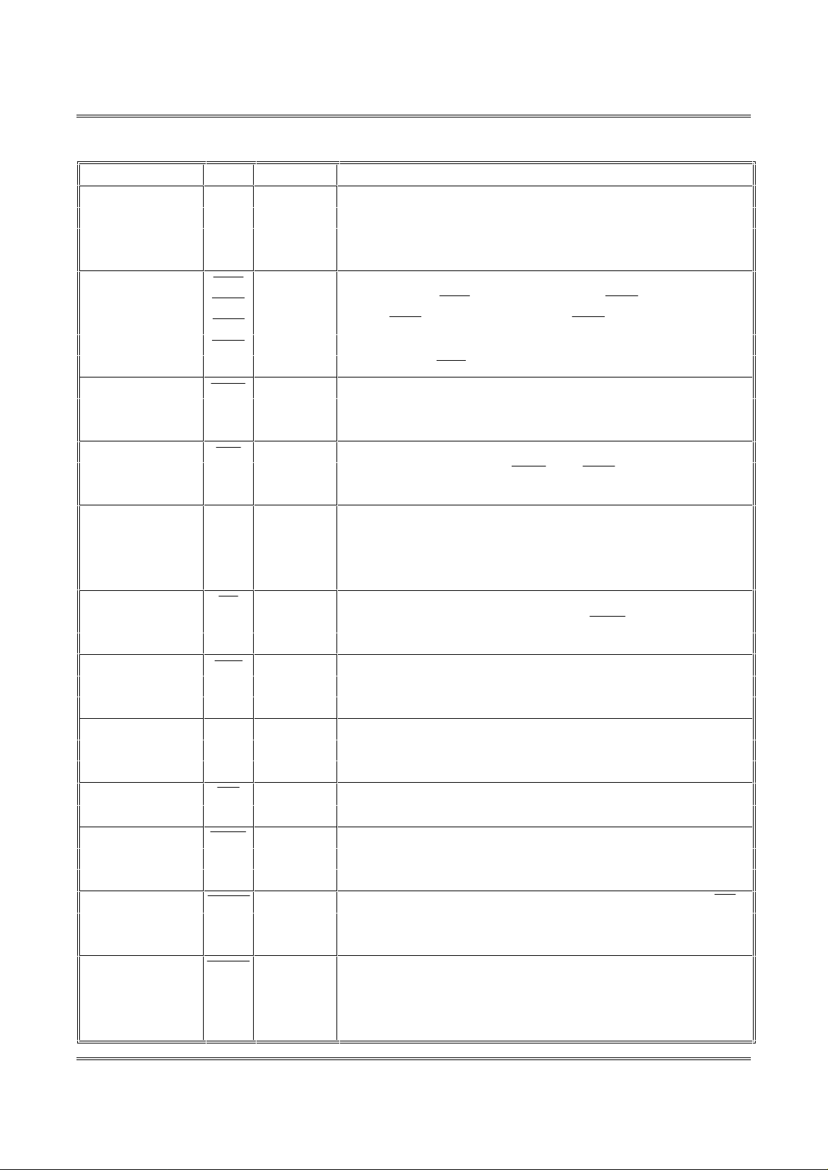
PIN DESCRIPTIONS
QFP PINS SYM. TYPE DESCRIPTION
32-37, 44-49, A0- Input- Addresses: These inputs are registered and must meet the setup and
81, 82, 99, 100, A15 Synchronous hold times around the rising edge of CLK. The burst counter -
generates internal addresses associated with A0 and A1,during
burst cycle and wait cycle.
93-96
conditioned by
87
88
89 CLK Input- Clock: This signal registers the addresses, data, chip enables, write
98
92
97 CE2 Input- Synchronous Chip Enable: This active HIGH input is used to enable
86
83
84
85
Input- Byte Write: A byte write is LOW for a WRITE cyle and HIGH for
Synchronous a READ cycle.
DQ16.
Data I/O are high impedance if either of these inputs are LOW ,
Input- Write Enable: This active LOW input gates byte write operations
Synchronous and must meet the setup and hold times around the rising edge of
CLK.
Input- Global Write: This active LOW input allows a full 32-bit WRITE
Synchronous to occur independent of the
the setup and hold times around the rising edge of CLK.
Synchronous control and burst control inputs on its rising edge. All synchronous
inputs must meet setup and hold times around the clock's rising
edge.
Input- Synchronous Chip Enable: This active LOW input is used to enable
Synchronous the device and conditions internal use of
sampled only when a new external address is loaded.
Input- Synchronous Chip Enable: This active LOW input is used to enable
Synchronous the device. This input is sampled only when a new external address
is loaded. This input can be used for memory depth expansion.
Synchronous the device. This input is sampled only when a new external address
is loaded. This input can be used for memory depth expansion.
Input Output enable: This active LOW asynchronous input enables the
data output drivers.
Input- Address Advance: This active LOW input is used to control the
Synchronous internal burst counter. A HIGH on this pin generates wait cycle
(no address advance).
Input-
Synchronous being LOW, causes a new external address to be registered and a
Input- Address Status Controller:This active LOW input causes device to
Synchronous be deselected or selected along with new external address to be
Address Status Processor: This active LOW input, along with
READ cycle is initiated using the new address.
registered. A READ or WRITE cycle is initiated depending upon
write control inputs.
controls DQ17-DQ24.
controls DQ1-DQ8.
being LOW.
and
controls DQ9-
controls DQ25-DQ32.
lines and must meet
. This input is
Taiwan Memory Technology, Inc. reserves the right P. 3 Publication Date: DEC. 1998
to change products or specifications without notice. Revision:A
TE
C
H
tm
T35L6432A
PIN DESCRIPTIONS (continued)
QFP PINS SYM. TYPE DESCRIPTION
31 MODE Input- Mode: This input selects the burst sequence. A LOW on this pin
Static selects LINEAR BURST. A NC or HIGH on this pin selects
INTERLEAVED BURST. Do not alter input state while device is
operating.
64 ZZ Input Snooze Enable: This active HIGH asynchronous input causes the
device to enter a low-power standby mode in which all data in the
memory arry is retained.
2,3,6-9,12,13, 18, DQ1- Input/ Data Inputs/Outputs: First Byte is DQ1-DQ8. Second Byte is
19,22-25,28,29,52, DQ32 Output DQ9-DQ16. Third Byte is DQ17-DQ24. Fourth Byte is DQ2553,56-59,62,63,68, DQ32. Input data must meet setup and hold times around the
69,72-75,78,79, rising edge of CLK.
15,41,65,91 VCC Supply Power Supply: 3.3V +10%/-5%
17,40,67,90 VSS Ground Ground: GND
4,11,20,27,54,
61,70,77
5,10,21,26,55,
60,71,76
1,14,16,30,38,39, NC - No Connect: These signals are not internally conntected.
42,43,50,51,66,80
VCCQ I/O Supply Output Buffer Supply: 3.3V +10%/-5%
VSSQ I/O Ground Output Buffer Ground: GND
Taiwan Memory Technology, Inc. reserves the right P. 4 Publication Date: DEC. 1998
to change products or specifications without notice. Revision:A
TE
C
H
tm
GW
BWEBW1BW2BW3BW4
BWn
CE
BWn
OE
BWE
GW
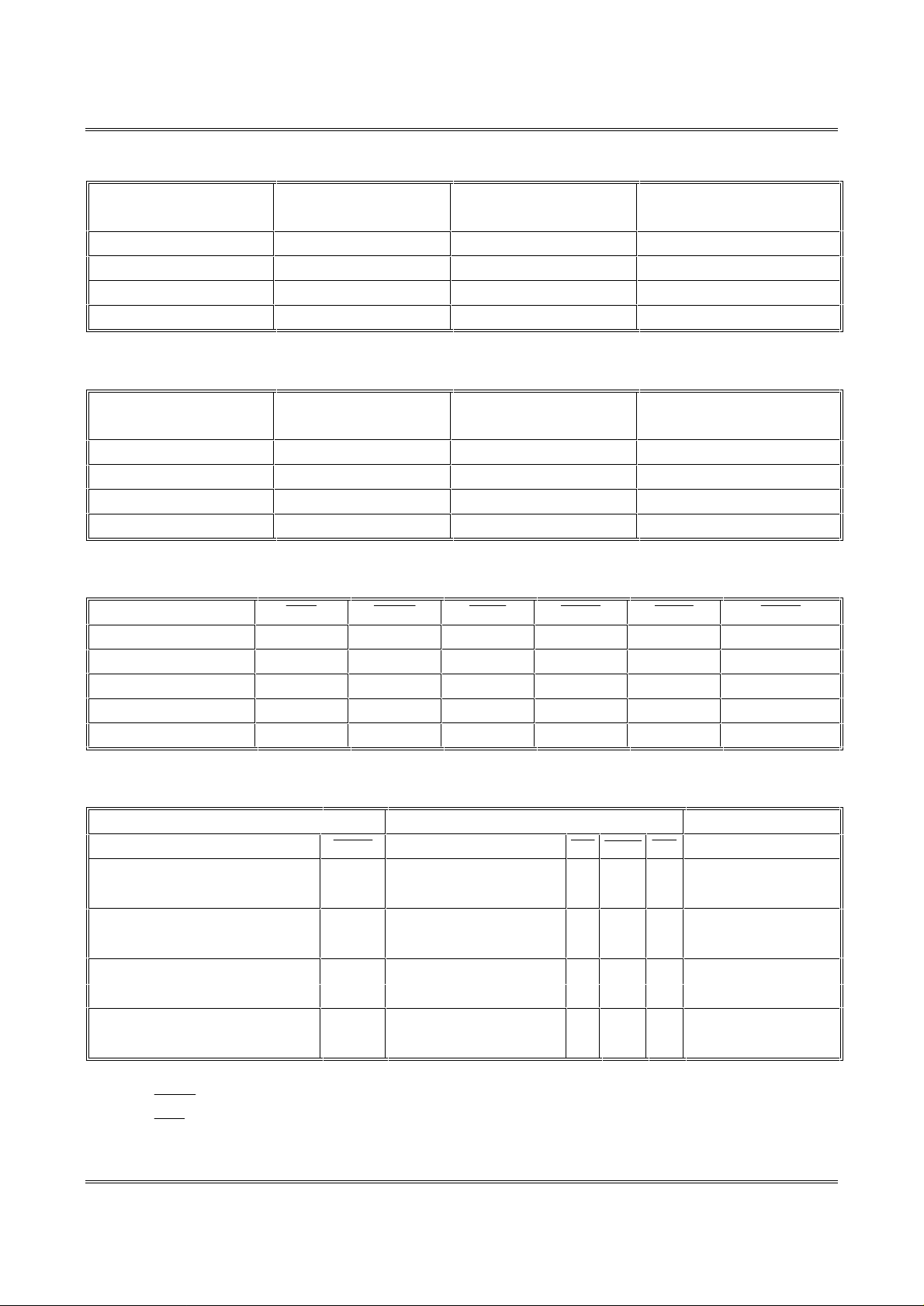
INTERLEAVED BURST ADDRESS TABLE (MODE = NC/VCC)
T35L6432A
First Address
(external)
A...A00 A...A01 A...A10 A...A11
A...A01 A...A00 A...A11 A...A10
A...A10 A...A11 A...A00 A...A01
A...A11 A...A10 A...A01 A...A00
Second Address
(internal)
Third Address
(internal)
Fourth Address
(internal)
LINEAR BURST ADDRESS TABLE (MODE = GND)
First Address
(external)
A...A00 A...A01 A...A10 A...A11
A...A01 A...A10 A...A11 A...A00
A...A10 A...A11 A...A00 A...A01
A...A11 A...A00 A...A01 A...A10
Second Address
(internal)
Third Address
(internal)
Fourth Address
(internal)
PARTIAL TRUTH TABLE FOR READ/WRITE
Function
READ H H X X X X
READ H L H H H H
WRITE one byte H L L H H H
WRITE all byte H L L L L L
WRITE all byte L X X X X X
WRITE PASS-THROUGH TRUTH TABLE
PREVIOUS CYCLE PRESENT CYCLE NEXT CYCLE
OPERATION
Initiate WRITE cycle, all bytes
Address= A(n-1), data= D(n-1) Register A(n), Q= D(n-1)
Initiate WRITE cycle, all bytes
Address= A(n-1), data= D(n-1) Q = D(n-1) previous cycle
Initiate WRITE cycle, all bytes
Address= A(n-1), data= D(n-1) Q = HIGH-Z previous cycle
Initiate WRITE cycle, one bytes
Address= A(n-1), data= D(n-1) Q = D(n-1) for one byte previous cycle
Note: 1. Previous cycle may be any cycle(non-burst, burst, or wait).
2.
3.
Taiwan Memory Technology, Inc. reserves the right P. 5 Publication Date: DEC. 1998
to change products or specifications without notice. Revision:A
is LOW for individual byte WRITE.
= LOW yields the same result for all-byte WRITE operation.
2,3
All L
2,3
All L
2,3
All L
ONE L
2
OPERATION
Initiate READ cycle L H L Read D(n)
No new cycle H H L No carry-over from
No new cycle H H H No carry-over from
No new cycle H H L No carry-over from
OPERATION
 Loading...