

TE
C
H
tm
FT
CE
CE2
ADSC
ADSP
ADV
BW1
BW2
BW3
BW4
BWE
GW
OE
ADSP
ADSC
ADV
BW1
BW2
BW3
BW4
BW1
BW2
BW3
BW4
BWE
GW
Preliminary T35L3232B
SYNCHRONOUS
BURST SRAM
FEATURES
¡E
¡E Fast Access times:
¡ESingle 3.3V +0.3V/-0.165V power supply
¡ECommon data inputs and data outputs
¡EIndividual BYTE WRITE ENABLE and
¡E Three chip enables for depth expansion and
¡E Clock-controlled and registered address, data
¡EInternally self-timed WRITE CYCLE
¡EBurst control pins ( interleaved or linear burst
¡EHigh 30pF output drive capability at rated
¡ESNOOZE MODE for reduced power standby
¡E Burst Sequence :
OPTIONS
through
Part Number Examples
pin for user configurable pipeline or
flow-through operation.
- Pipeline – 3.8 / 4 / 4.5 ns
- Flow-through – 9 / 10 / 11ns
GLOBAL WRITE control
address pipelining
I/Os and control signals
sequence)
access time
- Interleaved (MODE=NC or VCC)
- Linear (MODE=GND)
MARKING -3.8 -4 -4.5
Access
3-1-1-1
2-1-1-1
Package
PART NO. Pkg.
T35L3232B-3.8Q Q
T35L3232B-4T T
time
Cycle
time
Access
time
Cycle
time
100-pin QFP Q
100-pin TQFP T
3.8ns 4ns 4.5nsPipeline
6.6ns 7.5ns 8.5ns
9ns 10ns 11nsFlow-
10.5ns 15ns 15ns
32K x 32 SRAM
Pipeline and Flow-Through Burst Mode
GENERAL DESCRIPTION
The Taiwan Memory Technology Synchronous
Burst RAM family employs high-speed, low power
CMOS design using advanced triple-layer polysilicon,
double-layer metal technology. Each memory cell
consists of four transistors and two high valued resistors.
The T35L3232B SRAM integrates 32,768 x 32
bits SRAM cells with advanced synchronous peripheral
circuitry and a 2-bit counter for internal burst operation.
All synchronous inputs are gated by registers controlled
by a positive-edge-triggered clock input (CLK). The
synchronous inputs include all addresses, all data inputs,
address-pipelining chip enable (
expansion chip enables (
inputs (
(
global write (
(OE), Snooze enable (ZZ) and burst mode control
(MODE). The data outputs (Q), enabled by
also asynchronous.
either address status processor (
status controller (
addresses can be internally generated as controlled by
the burst advance pin (
to initiate self-timed WRITE cycle. WRITE cycles
can be one to four bytes wide as controlled by the write
control inputs. Individual byte write
allows individual byte to be written.
DQ1-DQ8.
controls DQ17-DQ 24.
with
all bytes to be written. WRITE pass-through
capability allows written data available at the output for
the immediately next READ cycle. This device also
incorporates pipelined enable circuit for easy depth
expansion without penalizing system performance.
,
Asynchronous inputs include the output enable
Addresses and chip enables are registered with
Address and write controls are registered on-chip
,
,
,
).
controls DQ9-DQ16.
,
being LOW.
, and
and CE2), burst control
, and
,
) input pins. Subsequent burst
, and
).
controls DQ25-DQ32.
can be active only
being LOW causes
), depth-
), write enables
), and
, are
) or address
controls
Taiwan Memory Technology, Inc. reserves the right P. 1 Publication Date: FEB. 2000
to change products or specifications without notice. Revision:0.A
TE
C
H
tm
Preliminary T35L3232B
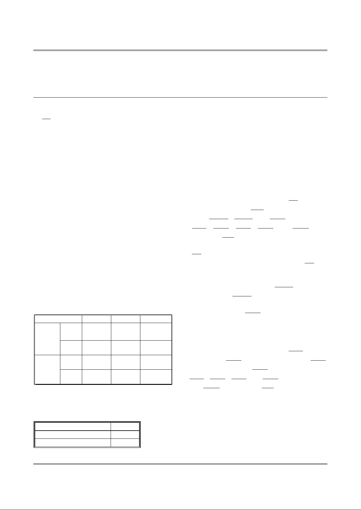
FUNCTIONAL BLOCK DIAGRAM
COUNTER
CLR
15
A0
BINARY
& LOGIC
A0-A14
MODE
ADV
CLK
ADSC
ADSP
15
ADDRESS
REGISTER
A1
Q1
Q0
13
15
A1'
A0'
BWE
BW4
BW3
BW2
BW1
GW
FT
CE
CE2
CE2
OE
BYTE 4
WRITE REGISTER
BYTE 3
WRITE REGISTER
BYTE 2
WRITE REGISTER
BYTE 1
WRITE REGISTER
ENABLE
REGISTER
8
BYTE 4
WRITE DRIVER
8
BYTE 3
WRITE DRIVER
8
BYTE 2
WRITE DRIVER
8
BYTE 1
WRITE DRIVER
8
8
8
8
32K x 8 x 4
MEMORY
ARRAY
32 32
SENSE
AMPS
OUTPUT
BUFFERS
4
32
INPUT
REGISTERS
DQ1
¡E
¡E
¡E
DQ32
Note: The Functional Block Diagram illustrates simplified device operation. See Truth Table, pin
descriptions and timing diagrams for detailed information.
Taiwan Memory Technology, Inc. reserves the right P. 2 Publication Date: FEB. 2000
to change products or specifications without notice. Revision:0.A
TE
C
H
tm
NC
VCC
NC
NC
A10
NC
VSS
A11
A12
A13
A14
NC
NC
MODE
Preliminary T35L3232B
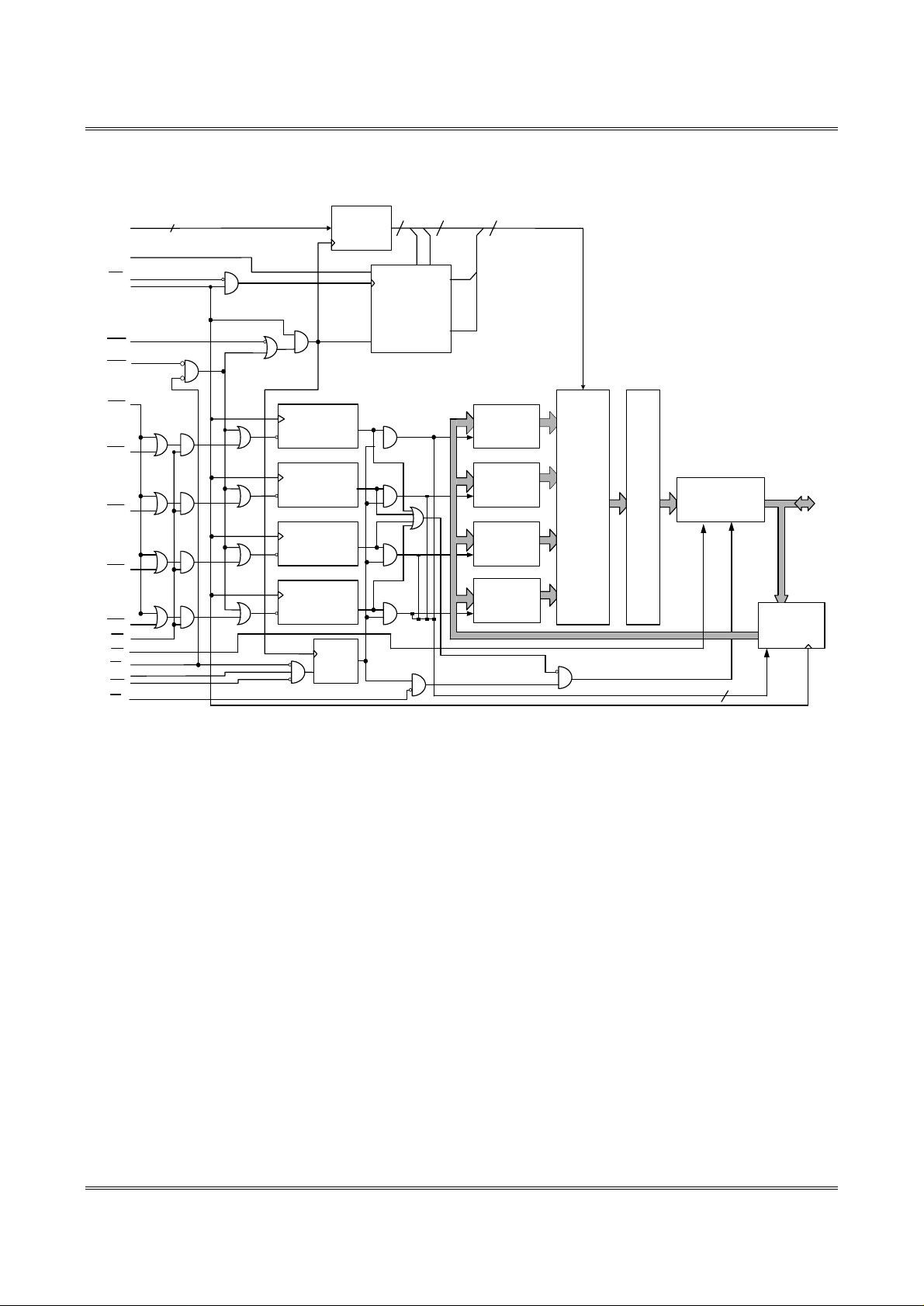
PIN ASSIGNMENT (Top View)
A7
A6
CE
CE2
BW4
9596 88 87 86 85 84 83 82 819091929394 89100 99 98 97
BW3
BW2
BW1
CE2
VCC
VSS
CLK
GW
BWE
OE
ADSC
ADSP
ADV
A8
A9
NC
DQ17
DQ18
VCCQ
VSSQ
DQ19
DQ20
DQ21
DQ22
VSSQ
VCCQ
DQ23
DQ24
FT
VCC
NC
VSS
DQ25
DQ26
VCCQ
VSSQ
DQ27
DQ28
DQ29
DQ30
VSSQ
VCCQ
DQ31
DQ32
NC NC
1
2
3
4
5
6
7
8
9
10
11
12
13
14
15
16
17
18
19
20
21
22
23
24
25
26
27
28
29
30
31 41403938373635343332 4948474645444342 50
100-pin QFP
or
100-pin TQFP
80
79
78
77
76
75
74
73
72
71
70
69
68
67
66
65
64
63
62
61
60
59
58
57
56
55
54
53
52
51
NC
DQ16
DQ15
VCCQ
VSSQ
DQ14
DQ13
DQ12
DQ11
VSSQ
VCCQ
DQ10
DQ9
VSS
NC
VCC
ZZ
DQ8
DQ7
VCCQ
VSSQ
DQ6
DQ5
DQ4
DQ3
VSSQ
VCCQ
DQ2
DQ1
A0
A1
A2
A3
A4
A5
Taiwan Memory Technology, Inc. reserves the right P. 3 Publication Date: FEB. 2000
to change products or specifications without notice. Revision:0.A
TE
C
H
tm
t
CE2
CE
CE2
CE
CE2
OE
PIPELINE READ TIMING
KC
C LK
tKHt
KL
t
ADS StADSH
AD S P
t
ADS StADSH
AD SC
tASt
AH
Preliminary T35L3232B
AD D R E S S
G W, B W E ,
B W 1 - B W 4
CE
( N O T E 2 )
AD V
O E
Q Q(A3)
t
CEStCEH
tWSt
(NOTE3)
High -Z
WH
t
KQLZ
t
KQ
Sing le READ
t
AAStAAH
ADV susp ends bur st.
t
t
OEQ
KQ
t
OEHZ
t
OELZ
KQX
(NOTE1)
BUR ST R EAD
t
Q(A1) Q(A2) Q(A2+1) Q(A2+2) Q(A2+3) Q(A2+1)
A3A2A1
Burst c ontinued wi th
new b ase add ress.
Q(A2)
Burst wra ps a round
to it s ini tal st ate.
Deselect cy cle.
t
KQHZ
t
KQX
DON'T CARE
UNDEFINED
Note: 1. Q(A2) refers to output from address A2. Q (A2 + 1) refers to output from the next internal burst
address following A2.
2.
and CE2 have timing identical to CE. On this diagram, when
and CE2 is HIGH. When
is HIGH,
is HIGH and CE2 is LOW.
is LOW,
is LOW
3. Timing is shown assuming that the device was not enabled before entering into this sequence.
does not cause Q to be driven until after the following clock rising edge.
Taiwan Memory Technology, Inc. reserves the right P. 12 Publication Date: FEB. 2000
to change products or specifications without notice. Revision:0.A
TE
C
H
tm
CE2
CE
CE2
CE
CE2
OE
t
FLOW-THROUGH READ TIMING
KC
CLK
tKHt
KL
t
AD S StAD SH
ADS P
t
AD S StAD SH
AD SC
tASt
AH
AD DRES S
GW , BWE ,
BW 1-B W4
CE
(NO TE 2)
A 1
t
CE StCE H
t
W StW H
A2
t
AAStAAH
Preliminary T35L3232B
De s ele c t C y c le
(NOTE 4)
ADV
AD V s uspe n ds burst.
O E
t
OEQ
t
t
KQ LZ
Q
High-Z
t
KQ
OEHZ
Q(A1) Q(A2) Q(A2+1) Q(A2+2) Q(A2+3) Q(A2+1)
Si ngle RE AD
t
OELZ
t
t
KQX
KQ
Q(A2)
(NOTE1 )
BU R ST R EA D
Burst w raps around to
it s init a l s ta te .
t
KQHZ
Q(A2+2)
DON'T CARE
UNDEFINED
Note: 1. Q(A2) refers to output from address A2. Q (A2 + 1) refers to output from the next internal burst
address following A2.
2.
and CE2 have timing identical to CE. On this diagram, when
and CE2 is HIGH. When
is HIGH,
is HIGH and CE2 is LOW.
is LOW,
is LOW
3. Timing is shown assuming that the device was not enabled before entering into this sequence.
does not cause Q to be driven until after the following clock rising edge.
4. Output are disabled tKQHZ after diselect.
Taiwan Memory Technology, Inc. reserves the right P. 13 Publication Date: FEB. 2000
to change products or specifications without notice. Revision:0.A
TE
C
H
tm
t
CE2
CE
CE2
CE
CE2
OE
ADV
GW
GW
BWE
BW1
BW4
WRITE TIMING
C L K
t
ADS StADSH
tKHt
Preliminary T35L3232B
KC
KL
AD S P
AD SC
AD D R E SS
B WE ,
B W 1 - B W 4
G W
CE
( N O T E 2 )
AD V
O E
t
ADS StADSH
tASt
AH
BYT E W RITE si gnal s a re
igno red fo r firs t cyc le wh en
ADS P in itial tes bu rst.
t
CEStCEH
(NOTE3)
tDSt
DH
tWSt
WH
(NOTE5)
ADSC exte nds bur st.
ADV s uspn ds b urst.(NOTE4)
t
ADSStADSH
A3A2A1
tWSt
t
AAStAAH
WH
D
Q
High -Z
BUR ST R EAD Exte nde d BU RST W RIT E
D(A1) D(A2) D(A2+1) D(A2+2) D(A2+3) D(A3+1)D(A3)
t
OEHZ
Sin gle WRI TE
(NOTE1)
D(A2+1) D(A3+2)
BUR ST W RIT E
DON'T CARE
UNDEFINED
Note: 1. Q(A2) refers to output from address A2. Q (A2 + 1) refers to output from the next internal burst
address following A2.
2.
3.
and CE2 have timing identical to CE. On this diagram, when
LOW and CE2 is HIGH. When
is HIGH ,
is HIGH and CE2 is LOW.
is LOW ,
must be HIGH before the input data setup and hold HIGH throughout the data hold time.
is
This prevents input/output data contention for the time period to the byte write enable inputs being
sampled.
4.
5. Full width WRITE can be initiated by
must be HIGH to permit a WRITE to the loaded address.
LOW or
HIGH and
,
-
LOW.
Taiwan Memory Technology, Inc. reserves the right P. 14 Publication Date: FEB. 2000
to change products or specifications without notice. Revision:0.A

TE
C
H
tm
t
CE2
CE
CE
CE2
CE
CE2
ADSP
ADSC
ADV
GW
ADSP
ADSC
PIPELINE READ/WRITE TIMING
KC
C LK
tKHt
KL
t
ADSStADSH
AD S P
AD SC
tASt
AH
Preliminary T35L3232B
A D D RES S
B WE
B W 1 - B W 4
CE
( N O T E 2 )
AD V
O E
A2 A6
tWSt
t
CEStCEH
t
KQ
D
High-Z
t
KQLZ
Q
High-Z
Q(A1) Q(A2) Q(A3) Q(A4) Q(A4+1) Q(A4+3)Q(A4+2)
Back-to-Bac k READs
t
DS
D(A3) D(A5) D(A6)
t
OEHZ
Sin gle W RIT E
A4
WH
t
DH
t
OELZ
t
KQ
Pass-through
READ
(NOTE1)
BURS T RE AD
A5A3A1
Back-to-Back
WRIT Es
DON'T CARE
UNDEFINED
Note: 1. Q(A4) refers to output from address A4. Q (A4 + 1) refers to output from the next internal burst
address following A4.
2.
3. The data bus (Q) remains in High-Z following a WRITE cycle unless an
and CE2 have timing identical to
LOW and CE2 is HIGH. When
. On this diagram, when
is HIGH,
is HIGH and CE2 is LOW.
is LOW,
,
is
or
cycle is performed.
4.
5. Back-to-back READs may be controlled by either
is HIGH.
or
.
Taiwan Memory Technology, Inc. reserves the right P. 15 Publication Date: FEB. 2000
to change products or specifications without notice. Revision:0.A
TE
C
H
tm
CE2
CE
CE
CE2
CE
CE2
ADSP
ADSC
ADV
GW
ADSP
ADSC
t
FLOW-THROUGH READ/WRITE TIMING
KC
CLK
tKHt
KL
t
ADSStAD SH
ADS P
AD SC
tASt
AH
Preliminary T35L3232B
AD DRE SS
BW E
BW 1- BW 4
(NOTE 4)
CE
(NOTE 2)
ADV
O E
A 2 A 6
t
W StW H
t
CEStCE H
t
DS
D
Q
High-Z
t
OE HZ
Q(A1) Q(A2) Q(A4) Q(A4+1) Q(A4+3)Q(A4+2)
Ba ck-to-B ack R EAD s Back-to-Back
D(A3) D(A5) D(A6)
Si ngle W R ITE
A 4
t
DH
t
OELZ
t
KQ
(NO TE1)
BUR ST R EAD
A 5A 3A 1
W RITEs
DON'T CARE
UNDEFINED
Note: 1. Q(A4) refers to output from address A4. Q (A4 + 1) refers to output from the next internal burst
address following A4.
2.
3. The data bus (Q) remains in High-Z following a WRITE cycle unless an
and CE2 have timing identical to
LOW and CE2 is HIGH. When
. On this diagram, when
is HIGH,
is HIGH and CE2 is LOW.
is LOW,
,
is
or
cycle is performed.
4.
5. Back-to-back READs may be controlled by either
is HIGH.
or
.
Taiwan Memory Technology, Inc. reserves the right P. 16 Publication Date: FEB. 2000
to change products or specifications without notice. Revision:0.A
TE
C
H
tm
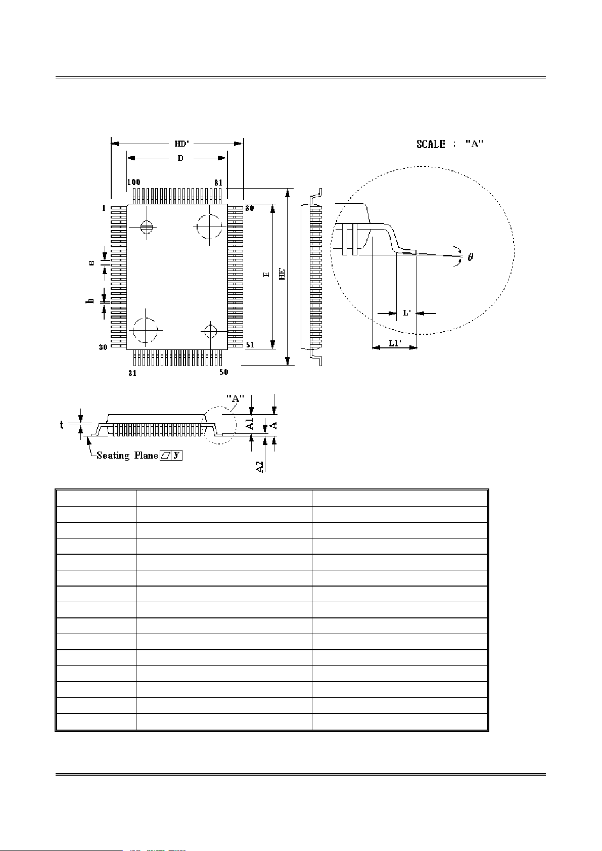
PACKAGE DIMENSIONS
100-LEAD QFP SSRAM (14 x 20 mm)
Preliminary T35L3232B
SYMBOL DIMENSIONS IN INCHES DIMENTION IN MM
A 0.130(MAX) 3.302(MAX)
A1
A2 0.004(MIN) 0.102(MIN)
b 0.012+0.004-0.002 0.300+0.102-0.051
D
E
e
HD'
HE'
L'
L1'
t 0.006+0.004-0.002 0.150+0.102-0.051
y 0.004(MAX) 0.102(MAX)
£c
Taiwan Memory Technology, Inc. reserves the right P.17 Publication Date: FEB. 2000
to change products or specifications without notice. Revision:0.A
0.112¡Ó0.005 2.845¡Ó0.127
0.551¡Ó0.005 14.000¡Ó0.127
0.787¡Ó0.005 20.000¡Ó0.127
0.026¡Ó0.006 0.650¡Ó0.152
0.677¡Ó0.008 17.200¡Ó0.203
0.913¡Ó0.008 23.200¡Ó0.203
0.032¡Ó0.008 0.800¡Ó0.203
0.063¡Ó0.008 1.600¡Ó0.203
0¡C~12
¡C
0¡C~12
¡C
TE
C
H
tm
PACKAGE DIMENSIONS
100-LEAD TQFP SSRAM (14 x 20 mm)
Preliminary T35L3232B
SYMBOL DIMENSIONS IN INCHES DIMENTION IN MM
A 0.063(MAX) 1.600(MAX)
A1
A2 0.002(MIN) 0.050(MIN)
b 0.013+0.002-0.004 0.320+0.060-0.100
D
E
e
HD'
HE'
L'
L1'
t
y 0.003(MAX) 0.080(MAX)
£c
0.055¡Ó0.005 1.400¡Ó0.050
0.551¡Ó0.004 14.000¡Ó0.100
0.787¡Ó0.004 20.000¡Ó0.100
0.026¡Ó0.006 0.650¡Ó0.152
0.630¡Ó0.004 16.000¡Ó0.100
0.866¡Ó0.004 22.000¡Ó0.100
0.024¡Ó0.006 0.600¡Ó0.150
0.039¡Ó0.006 1.000¡Ó0.150
0.006¡Ó0.002
¡C
0¡C~7
0.150+0.050-0.060
¡C
0¡C~7
Taiwan Memory Technology, Inc. reserves the right P.18 Publication Date: FEB. 2000
to change products or specifications without notice. Revision:0.A

TE
C
H
tm
Addresses: These inputs are registered and must meet the setup and
hold times around the rising edge of CLK. The burst counter
s associated with A0 and A1, during
BW1
BW2
BW3
BW4
Byte Writes: A byte write is LOW for a WRITE cyle and HIGH for
BW1
BW2
BW3
BW4
DQ32.
Data I/O are high impedance if either of these inputs are LOW ,
BWE
BWE
Write Enable: This active LOW input gates byte write operations
and must meet the setup and hold times around the rising edge of
GW
bit WRITE to
BWE
BWn
lines and must meet
dresses, data, chip enables,
writecontrol and burst control inputs on its rising edge. All
synchronous inputs must meet setup and hold times around the
CE
W input is used to enable
ADSP
. This input is
CE2
to enable
the device. This input is sampled only when a new external address
Synchronous Chip Enable: This active HIGH input is used to enable
s sampled only when a new external address
OE
ADV
ADSP
CE
PIN DESCRIPTIONS
PINS SYM. TYPE DESCRIPTION
32-37, 44-48,
81, 82, 99,
100,
93-96
A0-A14
Input-
Synchronous
Input-
Synchronous
generates internal addresse
burst cycle and wait cycle.
a READ cycle.
DQ16.
conditioned by
Preliminary T35L3232B
controls DQ1-DQ8.
controls DQ17-DQ24.
being LOW.
controls DQ9-
controls DQ25-
87
88
89 CLK
98
92
97 CE2
Input-
Synchronous
Input-
Synchronous
Input-
Synchronous
Input-
Synchronous
Input-
Synchronous
Input-
Synchronous
CLK.
Global Write: This active LOW input allows a full 32-
occur independent of the
the setup and hold times around the rising edge of CLK.
Clock: This signal registers the ad
clock's rising edge.
Synchronous Chip Enable: This active LO
the device and conditions internal use of
sampled only when a new external address is loaded.
Synchronous Chip Enable: This active LOW input is used
is loaded. This input can be used for memory depth expansion.
the device. This input i
is loaded. This input can be used for memory depth expansion.
and
86
83
84
Taiwan Memory Technology, Inc. reserves the right P. 4 Publication Date: FEB. 2000
to change products or specifications without notice. Revision:0.A
Input
Input-
Synchronous
Input-
Synchronous
Output enable: This active LOW asynchronous input enables the
data output drivers.
Address Advance: This active LOW input is used to control the
internal burst counter. A HIGH on this pin generates wait cycle
(no address advance).
Address Status Processor: This active LOW input, along with
being LOW, causes a new external address to be registered and a
READ cycle is initiated using the new address.
TE
C
H
tm
ADSC
us Controller:This active LOW input causes
device to be deselected or selected along with new external
address to be registered. A READ or WRITE cycle is
FT
through mode. A NC or
Mode: This input selects the burst sequence. A LOW on this
pin selects LINEAR BURST. A NC or HIGH on this pin
input state
Snooze Enable: This active HIGH asynchronous input causes
power standby mode in which all
9, 12, 13,
PIN DESCRIPTIONS (continued)
QFP PINS SYM. TYPE DESCRIPTION
85
Input-
Synchronous
Address Stat
initiated depending upon write control inputs.
Preliminary T35L3232B
14
2, 3, 6-
31 MODE
64 ZZ Input
18, 19, 22-25,
28, 29, 52, 53,
56-59, 62, 63,
68, 69, 72-75,
78, 79,
15,41,65,91 VCC Supply Power Supply: 3.3V +10%/-5%
17,40,67,90 VSS Ground Ground: GND
4,11,20,27,54,
61,70,77
5,10,21,26,55,
60,71,76
DQ1-
DQ32
VCCQ I/O Supply Output Buffer Supply: 3.3V +10%/-5%
VSSQ I/O Ground Output Buffer Ground: GND
Input-
Static
Input-
Static
Input/
Output
A LOW on this pin selects in flowHIGH on this pin selects in pipeline mode.
selects INTERLEAVED BURST. Do not alter
while device is operating.
the device to enter a lowdata in the memory arry is retained.
Data Inputs/Outputs: First Byte is DQ1-DQ8. Second Byte is
DQ9-DQ16. Third Byte is DQ17-DQ24. Fourth Byte is DQ25DQ32. Input data must meet setup and hold times around the
rising edge of CLK.
1,16,30,38,
39,42,43,49,
50, 51, 66,80
Taiwan Memory Technology, Inc. reserves the right P. 5 Publication Date: FEB. 2000
to change products or specifications without notice. Revision:0.A
NC - No Connect: These signals are not internally conntected.
TE
C
H
tm
GW
BWE
BW1
BW2
BW3
BW4
Preliminary T35L3232B
INTERLEAVED BURST ADDRESS TABLE (MODE = NC/VCC)
First Address
(external)
A...A00 A...A01 A...A10 A...A11
A...A01 A...A00 A...A11 A...A10
A...A10 A...A11 A...A00 A...A01
A...A11 A...A10 A...A01 A...A00
Second Address
(internal)
Third Address
(internal)
Fourth Address
(internal)
LINEAR BURST ADDRESS TABLE (MODE = GND)
First Address
(external)
A...A00 A...A01 A...A10 A...A11
A...A01 A...A10 A...A11 A...A00
A...A10 A...A11 A...A00 A...A01
A...A11 A...A00 A...A01 A...A10
Second Address
(internal)
Third Address
(internal)
Fourth Address
(internal)
PARTIAL TRUTH TABLE FOR READ/WRITE
Function
READ H H X X X X
READ H L H H H H
WRITE one byte H L L H H H
WRITE all byte H L L L L L
WRITE all byte L X X X X X
Taiwan Memory Technology, Inc. reserves the right P. 6 Publication Date: FEB. 2000
to change products or specifications without notice. Revision:0.A

TE
C
H
tm
CE
CE2
ADSP
ADSC
ADV
WRITE
OE
WRITE
BW1
BW2
BW3
BW4
BWE
GW
WRITE
BW1
BW2
BW3
BW4
OE
OE
OE
ADSP
TRUTH TABLE
Preliminary T35L3232B
OPERATION
, Power Down None L X L L L X X X X L-H High-Z
Snooze Cycle, Power Down None X X X H X X X X X X High-Z
READ Cycle, Begin Burst External L L H L L X X X L L-H Q
READ Cycle, Begin Burst External L L H L L X X X H L-H High-Z
WRITE Cycle, Begin Burst External L L H L H L X L X L-H D
READ Cycle, Begin Burst External L L H L H L X H L L-H Q
READ Cycle, Begin Burst External L L H L H L X H H L-H High-Z
READ Cycle, Continue Burst Next X X X L H H L H L L-H Q
READ Cycle, Continue Burst Next X X X L H H L H H L-H High-Z
READ Cycle, Continue Burst Next H X X L X H L H L L-H Q
READ Cycle, Continue Burst Next H X X L X H L H H L-H High-Z
WRITE Cycle, Continue Burst Next X X X L H H L L X L-H D
WRITE Cycle, Continue Burst Next H X X L X H L L X L-H D
READ Cycle, Suspend Burst Current X X X L H H H H L L-H Q
READ Cycle, Suspend Burst Current X X X L H H H H H L-H High-Z
READ Cycle, Suspend Burst Current H X X L X H H H L L-H Q
READ Cycle, Suspend Burst Current H X X L X H H H H L-H High-Z
WRITE Cycle, Suspend Burst Current X X X L H H H L X L-H D
WRITE Cycle, Suspend Burst Current H X X L X H H L X L-H D
ADDRESS
USED
None H X X L X L X X X L-H High-Z
None L H X L L X X X X L-H High-Z
None L X L L H L X X X L-H High-Z
None L H X L H L X X X L-H High-Z
CE2 ZZ
CLK DQ
Note: 1. X means "don't care." H means logic HIGH. L means logic LOW.
or more byte write enable signals (
equals LOW.
2.
3. All inputs except
4. Suspending burst generates wait cycle.
5. For a write operation following a read operation.
6. This device contains circuitry that will ensure the outputs will be High-Z during power-up.
7.
= enables write to DQ1-DQ8.
to DQ17-DQ24.
to HIGH) of CLK.
required setup time plus High-Z time for
hold time.
= LOW along with chip being selected always initiates an internal READ cycle at the L-H
edge of CLK. A WRITE cycle can be performed by setting WRITE LOW for the CLK L-H
edge of the subsequent wait cycle. Refer to WRITE timing diagram for clarification.
= H means all byte write signal are HIGH.
=enables write to DQ25-DQ32.
and ZZ must meet setup and hold times around the rising edge ( LOW
,
= enables write to DQ9-DQ16.
,
and staying HIGH throughout the input data
or
must be HIGH before the input data
) and
= L means any one
are LOW, or
= enables write
Taiwan Memory Technology, Inc. reserves the right P.7 Publication Date: FEB. 2000
to change products or specifications without notice. Revision:0.A

TE
C
H
tm
ADSC
ADSP
ADV
GW,BWE
Preliminary T35L3232B
ABSOLUTE MAXIMUM RATINGS*
Voltage on VCC Supply Relative to VSS.
…………-0.5V to +4.6V
I/O Supply Voltage VccQ ........... Vss -0.5V to Vcc
V
......................................... -0.5V to Vcc +0.5V
IN
Storage Temperature (plastic)...... -55°C to +150°C
Junction Temperature ..........….................. +150°C
Power Dissipation ........................................ 1.0W
Short Circuit Output Current...................... 100mA
DC ELECTRICAL CHARACTERISTICS AND RECOMMENDED
OPERATING CONDITIONS
(0°C ≤ Ta ≤ 70°C; VCC = 3.3V +10%/-5% unless otherwise noted)
DESCRIPTION CONDITIONS SYM. MIN MAX UNITS NOTES
Input High (Logic)
voltage
Input Low (Logic)
voltage
Input Leakage Current
Output Leakage Current Output(s) disabled, 0V
Output High Voltage IOH = -4.0 mA V
Output Low Voltage IOL = 8.0 mA V
Supply Voltage Vcc 3.1 3.6 V 1
0V ≤ VIN≤ VCC
≤ V
OUT
≤ VCC
*Stresses greater than those listed under
"Absolute Maximum Ratings" may cause
permanent damage to the device. This is a stress
rating only and functional operation of the device
at these or any other conditions above those
indicated in the operational sections of this
specification is not implied. Exposure to absolute
maximum rating conditions for extended periods
may affect reliability.
V
V
I
IH
I
LI
LO
OH
OL
IL
2 VCCQ + 0.3 V 1, 2
-0.3 0.8 V 1, 2
-2 2
-2 2
2.4 V 1, 11
0.4 V 1, 11
µA
µA
14
MAX.
DESCRIPTION CONDITIONS SYM. TYP -3.8 -4 -4.5 UNITS NOTES
Device selected; all inputs ≤VIL or
Power Supply
Current : Operating
Power Supply
Current: Idle
CMOS Standby
TTL Standby
Clock Running
≥ VIH; cycle time ≥tKC MIN; VCC
= MAX; outputs open
Device selected;
,
inputs≤VIL or≥VIH; VCC = MAX;
cycle time ≥ tKC MIN: outputs open
Device deselected; VCC = MAX; all
inputs ≤ VSS + 0.2 or ≥ VCC - 0.2;
all inputs static; CLK frequency =0
Device deselected; all inputs ≤ V
or ≥ VIH; all inputs static; VCC =
MAX;CLK frequency = 0
Device deselected; all inputs ≤ V
or ≥ VIH; VCC =MAX; CLK cycle
time ≥tKCMIN
,
≥ VIH; all other
,
IL
IL
I
CC
I
SB1
I
SB2
I
SB3
I
SB4
TBD 250 200 150 mA 3, 12, 13
TBD 60 60 60 mA 12, 13
TBD 10 10 10 mA 12, 13
TBD 25 25 25 mA 12, 13
TBD 60 60 60 mA 12, 13
Taiwan Memory Technology, Inc. reserves the right P.8 Publication Date: FEB. 2000
to change products or specifications without notice. Revision:0.A

TE
C
H
tm
ADSC
ADSP
ADV
BW1
BW4
BWE
GW
CE2
ADSC
ADSP
ADV
BW1
BW4
BWE
GW
CE2
Preliminary T35L3232B
AC ELECTRICAL CHARACTERISTICS (Note 5) (0°C≤T
-3.8 -4 -4.5DESCRIPTION
SYM. MIN MAX MIN MAX MIN MAX
Clock(pipeline)
Clock cycle time t
Clock to output valid t
Clock to output invalid t
Clock to output in Low-Z t
Clock(flow-through)
Clock cycle time t
Clock to output valid t
Clock to output invalid t
Clock to output in Low-Z t
Output Times
Clock HIGH time t
Clock LOW time t
Clock to output in High-Z t
OE to output valid t
OE to output in Low-Z t
OE to output in High-Z t
Setup Times
Address t
,
Address Advance (
Byte Write Enables
(
~
Data-in t
Chip Enables(CE,
Hold Times
Address t
Address Advance (
Byte Write Enables
(
~
Data-in t
Chip Enables(CE,
,
,
,
,
,
)
)
)
,CE2)
)
)
)
,CE2)
KC
KQ
KQX
KQLZ
KC
KQ
KQX
KQLZ
KH
KL
KQHZ
OEQ
OELZ
OEHZ
AS
t
ADSS
t
AAS
t
WS
DS
t
CES
AH
t
ADSH
t
AAH
t
WH
DH
t
CEH
6.6 7.5 8.5 ns
3.8 4 4.5
1.5 2 2 ns
1.5 2 2 ns
10.5 15 15 ns
9.0 10 11
3 3 3 ns
3 3 3 ns
1.8 1.9 2.0 ns
1.8 1.9 2.0 ns 6, 7
5 5 5 ns 6, 7
5 5 5 ns 9
0 0 0 ns 6, 7
5 5 5 ns 6, 7
1.7
1.7 2.0 2.0
1.7 2.0 2.0
1.7 2.0 2.0
1.7 2.0 2.0
1.7 2.0 2.0
0.5 0.5 0.5 ns 8, 10
0.5 0.5 0.5 ns 8, 10
0.5 0.5 0.5 ns 8, 10
0.5 0.5 0.5 ns 8, 10
0.5 0.5 0.5 ns 8, 10
0.5 0.5 0.5 ns 8, 10
2.0
≤70°C;VCC=3.3V +0.3V/-0.165V)
A
UNITS NOTES
2.0 ns 8, 10
ns 8, 10
ns 8, 10
ns 8, 10
ns 8, 10
ns 8, 10
Taiwan Memory Technology, Inc. reserves the right P.9 Publication Date: FEB. 2000
to change products or specifications without notice. Revision:0.A

TE
C
H
tm
ADSP
OE
Preliminary T35L3232B
CAPACITANCE
DESCRIPTION CONDITIONS SYM. TYP MAX UNITS NOTES
Input Capacitance
Input/ Output
Capacitance(DQ)
TA = 25°C; f = 1 MHz
VCC = 3.3V
THERMAL CONSIDERATION
DESCRIPTION CONDITIONS SYM. QFP TYP UNITS NOTES
- Junction to Ambient
Thermal Resistance - Junction to Case
Still air, soldered on
4.25x1.125 inch 4-layer
AC TEST CONDITIONS
Input pulse levels 0V to 3.0V
Input rise and fall times 1.5ns
Input timing reference levels 1.5V
Output reference levels 1.5V
Output load See Figures 1 and
Notes:
1. All voltages referenced to VSS (GND).
2. Overshoot: VIH≤ +3.6 V for t ≤tKC/2.
Undershoot: VIL≤ -1.0 V for t ≤tKC/2.
3. Icc is given with no output current. Icc increases
with greater output loading and faster cycle
times.
4. This parameter is sampled.
5. Test conditions as specified with the output
loading as shown in Fig. 1 unless otherwise
noted.
6. Output loading is specified with CL = 5 pF as in
Fig. 2.
PCB
2
C
I
C
O
7. At any given temperature and voltage condition,
t
KQHZ is less than tKQLZ and tOEHZ is less
than tOELZ.
8. A READ cycle is defined by byte write enables
all HIGH or
enables being active for the required setup and
hold times. A WRITE cycle is defined by at one
byte or all byte WRITE per READ/WRITE
TRUTH TABLE.
9.
10.This is a synchronous device. All synchronous
11.AC I/O curves are available upon request.
12."Device Deselected means the device is in
13.Typical values are measured at 3.3V, 25°C and
14.MODE pin has an internal pull-up and exhibits
is a "don't care" when a byte write enable
is sampled LOW.
inputs must meet specified setup and hold time,
except for "don't care" as defined in the truth
table.
POWER-DOWN mode as defined in the truth
table. "Device Selected" means the device is
active.
20ns cycle time.
an input leakage current of ± 10µA.
3 4 pF 4
6 7 pF 4
Θ
Θ
JA
JB
20
1
°C/W
°C/W
LOW along with chip
OUTPUT LOADS
Taiwan Memory Technology, Inc. reserves the right P.10 Publication Date: FEB. 2000
to change products or specifications without notice. Revision:0.A

C
H
tm
DQ
TE
Preliminary T35L3232B
DQ
50
ohm
Z0 = 50 ohm
Fig. 1 output load equivalent Fig. 2 output load equivalent
Vt = 1.5V
351
ohm
3.3V
317
ohm
5 pF
Taiwan Memory Technology, Inc. reserves the right P.11 Publication Date: FEB. 2000
to change products or specifications without notice. Revision:0.A

TE
C
H
tm
CE
Preliminary T35L3232B
SNOOZE MODE
SNOOZE MODE is a low current, “power
down” mode in which the device is deselected and
current is reduced to I
The duration of
ZZ.
SNOOZE MODE is dictated by the length of time
the ZZ pin is in a HIGH state. After entering
SNOOZE MODE, the clock and all other inputs
are ignored. The ZZ pin (pin 64) is an
asynchronous, active HIGH input that causes the
SNOOZE MODE ELECTRICAL CHARACTERISTICS
DESCRIPTION CONDITIONS SYMBOL MIN MAX UNITS NOTES
Current during
SNOOZE MODE
ZZ HIGH to
SNOOZE MODE time t
SNOOZE MODE
Operation Recovery Time t
ZZ ≥ V
IH
device to enter SNOOZE MODE. When the ZZ
pin becomes a logic HIGH, I
is guaranteed after
ZZ
the setup time tZZ is met. Any access pending
when entering SNOOZE MODE is not guaranteed
to successfully complete. Therefore, SNOOZE
MODE must not be initiated until valid pending
operations are completed.
I
ZZ
ZZ 2(tKC)
RZZ 2(tKC)
5 mA
ns 4
ns 4
SNOOZE MODE WAVEFORM
C L K
CE
Z Z
t
ZZ
I
S UP PLY
Note: 1. The
2. All other inputs held to static CMOS levels (VIN ≤ Vss + 0.2 V or ≥ Vcc -0.2 V).
signal shown above refers to a TRUE state on all chip selects for the device.
I
Z Z
t
RZZ
DON'T CARE
I
SU PPLY
Taiwan Memory Technology, Inc. reserves the right P.12 Publication Date: FEB. 2000
to change products or specifications without notice. Revision:0.A
 Loading...