

Taiwan Memory Technology T15M256B-85RI, T15M256B-85R, T15M256B-85P, T15M256B-85PI, T15M256B-85DI Datasheet
...
TE
CH
tm
T15M256B
TM Technology Inc. reserves the right P. 1 Publication Date: MAY. 2002
to change products or specifications without notice. Revision:A
SRAM
32K X 8 LOW POWER
CMOS STATIC RAM
FEATURES
• High speed access time: 50/70/85/100ns
• Low power supply current :
- Operating :35mA(max)
- Standby : 10uA
• Power supply : 5V (± 10%)
• Fully static operation – No clock or refreshing
required
• All inputs and outputs directly LVTTL
compatible
• Common I/O capability
• Data retention voltage : 1.5V (min)
• Available packages :
28-pin DIP(600mil),SOJ, SOP, TSOP-I
(8x13.4mm forward type and reverse type).
•
Operating temperature :
- 0 ~ +70 °C
- -40 ~ +85 °C
PART NUMBER EXAMPLES
PART NO.
PACKAGE
CODE
Operating
Temperature
T15M256B-70N
T15M256B-70J
T15M256B-70D
T15M256B-85P
T15M256B-85R
N=DIP
J=SOJ
D=SOP
P=
TSOP-I(Forward)
R= TSOP-I(Reverse)
0 ~ +70 °C
T15M256B-70NI
T15M256B-70JI
T15M256B-70DI
T15M256B-85PI
T15M256B-85RI
N=DIP
J=SOJ
D=SOP
P=
TSOP-I(Forward)
R= TSOP-I(Reverse)
-40 ~ +85 °C
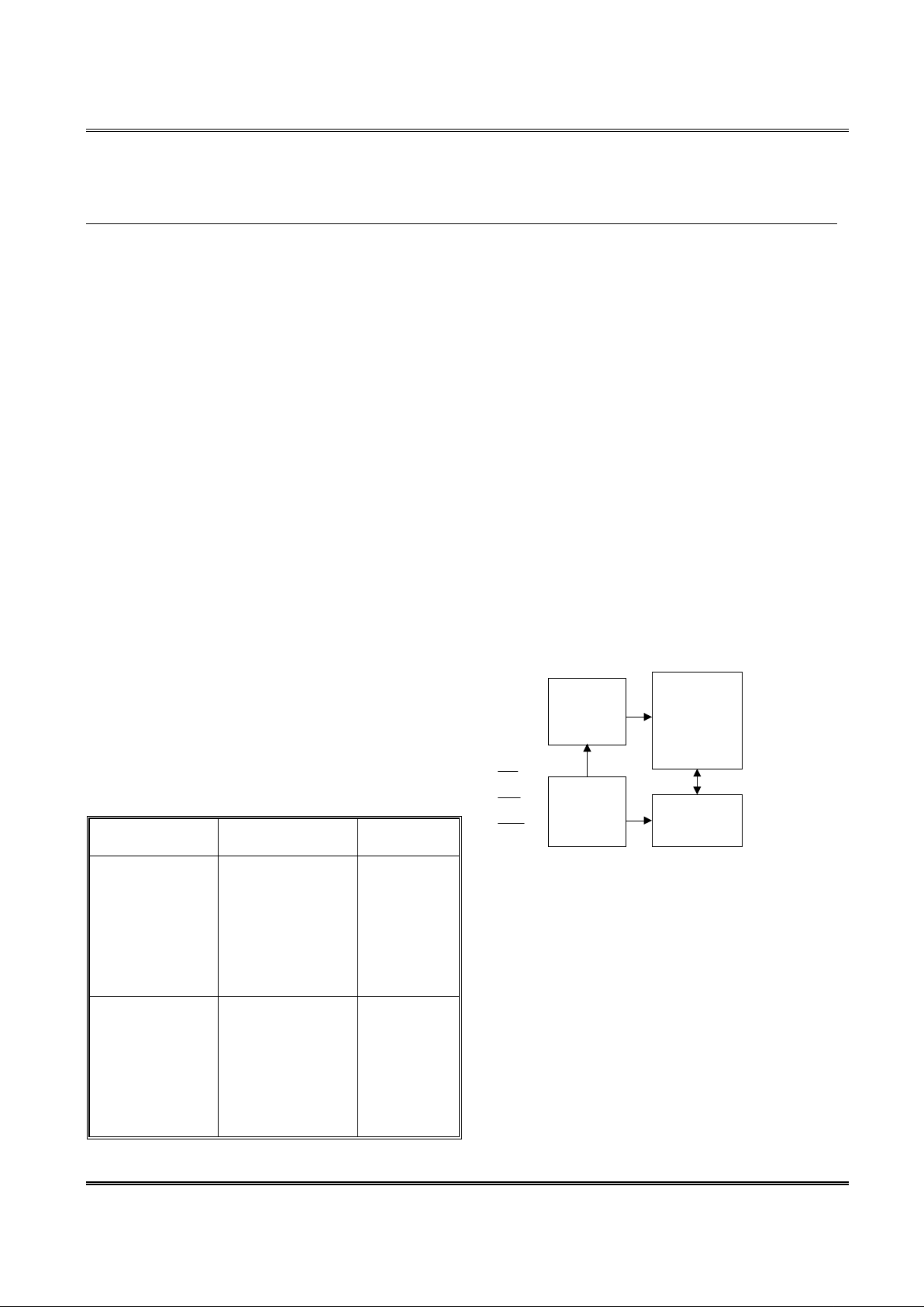
GENERAL DESCRIPTION
The T15M256B is a low power CMOS static
RAM. organized as 32,768 x 8 bits that operates
on a single 5-volt power supply. Low operating
and standby current . Data retention is guaranteed
at a power supply voltage as low as 1.5V. This
device is packaged in a standard 28-pin
DIP(600mil), SOJ, SOP, TSOP-I forward and
reverse type.
BLOCK DIAGRAM
DECODER
CONTROL
A0
→
A14 →
CS
→
OE
→
WE
→
←
I/O1
←
I/O8
Vcc →
DATA I/O
CORE
ARRAY
→Vss
.
.
.
.
.
TE
CH
tm
T15M256B
TM Technology Inc. reserves the right P. 2 Publication Date: MAY. 2002
to change products or specifications without notice. Revision:A
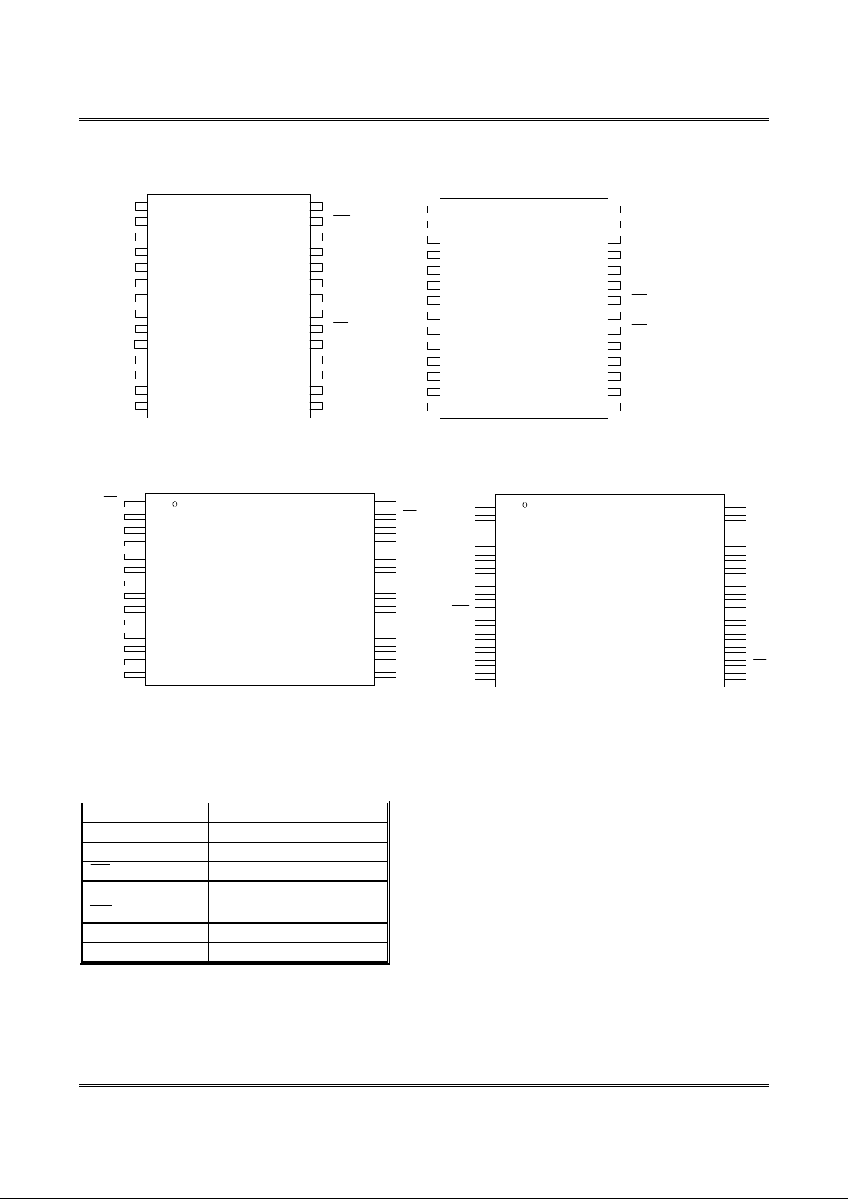
PIN CONFIGURATION
A1 2
A1 4
A7
A6
A5
A3
A4
A2
A1
A0
I/O 1
I/O 2
I/O 3
Vs s
28
27
26
25
23
24
22
21
20
19
18
17
16
15
1
2
3
4
6
5
7
8
9
10
11
12
13
14
Vcc
A13
A8
A9
A11
A10
I/O8
I/O7
I/O6
I/O5
I/O4
WE
OE
CS
DIP
&
SOJ
A12
A14
A7
A6
A5
A3
A4
A2
A1
A0
I/O1
I/O2
I/O3
Vss
28
27
26
25
23
24
22
21
20
19
18
17
16
15
1
2
3
4
6
5
7
8
9
10
11
12
13
14
Vcc
A13
A8
A9
A11
A10
I/O8
I/O7
I/O6
I/O5
I/O4
WE
OE
CS
SOP
PIN DESCRIPTION
SYMBOL DESCRIPTION
A0 - A14 Address Inputs
I/O1 - I/O8 Data Inputs/Outputs
CS
Chip Select Inputs
WE
Write Enable
OE
Output Enable
Vcc Power Supply
Vss Ground
TSOP-I
Forward
1
2
3
4
5
6
7
8
9
10
11
12
13
14
28
27
26
25
24
23
22
21
20
19
18
17
16
15
OE
A11
A9
A8
A13
WE
VCC
A14
A12
A7
A6
A5
A4
A3
A10
CS
I/O8
I/O7
I/O6
I/O5
I/O4
VSS
I/O3
I/O2
I/O1
A0
A1
A2
TSOP-I
Reverse
1
2
3
4
5
6
7
8
9
10
11
12
13
14
28
27
26
25
24
23
22
21
20
19
18
17
16
15
A3
A4
A5
A6
A7
A12
A14
VCC
WE
A13
A8
A9
A11
OE
A2
A1
A0
I/O1
I/O2
I/O3
VSS
I/O4
I/O5
I/O6
I/O7
I/O8
CS
A10
TE
CH
tm
T15M256B
TM Technology Inc. reserves the right P. 3 Publication Date: MAY. 2002
to change products or specifications without notice. Revision:A
DC CHARACTERISTICS ABSOLUTE MAXIMUM RATINGS
PARAMETER RATING UNIT
Supply Voltage to Vss Potential -0.5 to + 7V V
Inputs to Vss Potential -0.5 to Vcc +0.5 V
Power Dissipation 0.7 W
Storage Temperature -60 to +150 °C
RECOMMENDED OPERATING CONDITIONS
PARAMETER SYM MIN TYP MAX UNIT
Supply Voltage Vcc 4.5 5 5.5 V
Input Voltage, low
V
IL
-0.3 - 0.8 V
Input Voltage, high
V
IH
2.2 - Vcc+0.3 V
Ambient Temperature
T
A
0/-40 - +70/+85 °C
TRUTH TABLE
CS OE WE
MODE I/O1- I/O8 Power
H X X Not Selected High-Z Standby
L H H Output Disable High-Z Active
L L H Read Data Out
Active
L X L Write Data In
Active
OPERATING CHARACTERISTICS
(Vcc = 5V /
± 10%
, Vss = 0V, Ta =
0 ~ +70 °C
/-40 to 85°C)
PARAMETER SYM. TEST CONDITIONS MIN. TYP. MAX. UNIT
Input Leakage Current
I
LI
Vin=Vss to Vcc - - 1 uA
Output Leakage Current
I
LO
V
I/O
=Vss to Vcc ,
CS
=
V
IH
or
OE
= VIH or WE = VIL
- - 1 uA
Output Low Voltage
V
OL
I
OL
= + 2.1mA
- - 0.4 V
Output High Voltage
V
OH
IOH= - 1.0mA
2.4 - - V
-50 - - 35 mA
-70 - - 30 mA
-85 - - 25 mA
Operating Power
Supply Current
Icc
CS=
V
IL
, I/O=0mA
Cycle = MIN.
Duty = 100%
-100
- - 20 mA
I
SB
CS
=VIH, Cycle=min, Duty=100%
- - 0.3 mA
Standby Power
Supply Current
I
SB1
CS ≥
V
cc
-0.2V
- - 10 uA
TE
CH
tm
T15M256B
TM Technology Inc. reserves the right P. 4 Publication Date: MAY. 2002
to change products or specifications without notice. Revision:A
CAPACITANCE
(Vcc = 5V /
± 10%
, Ta = 25°C, f = 1 MHz)
PARAMETER SYMBOL CONDITION MAX. UNIT
Input Capacitance
C
IN
V
IN
= 0V
6 pF
Input/ Output Capacitance
C
I/O
V
OUT
= 0V
8 pF
Note: These parameters are sampled but not 100% tested.
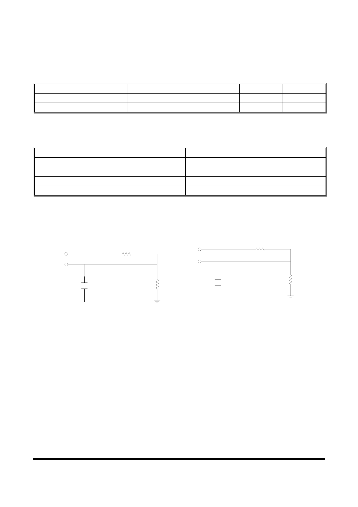
AC TEST CONDITIONS
PARAMETER CONDITIONS
Input Pulse Levels 0V to 3V
Input Rise and Fall Times 3 ns
Input and Output Timing Reference Level 1.5V
Output Load See Fig. 1,2
AC TEST LOADS AND WAVEFORM
R1 - 1928 ohm
5V
OUTPUT
30pF
Including
Jig and
Scope
R2
1020 ohm
R1- 1928 ohm
5V
OUTPUT
5pF
Including
Jig and
Scope
R2
1020
ohm
(For T
CLZ
, T
OLZ
, T
CHZ
, T
OHZ
, T
WHZ
, TOW )
Fig 1
Fig 2

TE
CH
tm
T15M256B
TM Technology Inc. reserves the right P. 5 Publication Date: MAY. 2002
to change products or specifications without notice. Revision:A
AC CHARACTERISTICS
(
V
cc
= 5V /
± 10%
, Vss = 0V, Ta =
0 ~ +70 °C/
-40 to 85°C)
(1) READ CYCLE
-50ns -70ns
-85ns -100ns
PARAMETER SYM.
MIN MAX MIN. MAX. MIN. MAX. MIN. MAX.
UNIT
Read Cycle Time
t
RC
50 - 70 - 85 - 100 - ns
Address Access Time
t
AA
- 50 - 70 - 85 - 100 ns
Chip Select Access Time
t
ACS
- 50 - 70 - 85 - 100 ns
Output Enable to Output Valid
t
AOE
- 25 - 35 - 40 - 50 ns
Chip Selection to Output in Low Z
t
CLZ*
7 - 10 - 10 - 10 - ns
Output Enable to Output in Low Z
t
OLZ*
5 - 5 - 5 - 5 - ns
Chip Deselection to Output in High Z
t
CHZ*
- 20 - 25 - 30 - 30 ns
Output Disable to Output in High Z
t
OHZ*
- 20 - 25 - 30 - 30 ns
Output Hold from Address Change
t
OH
10 - 10 - 10 - 10 - ns
* These parameters is measured with 5pF test load.
(2)WRITE CYCLE
-50ns -70ns -85ns -100ns
PARAMETER SYM.
MIN MAX MIN. MAX. MIN. MAX. MIN. MAX.
UNIT
Write Cycle Time
t
WC
50 - 70 - 85 - 100 - ns
Chip Selection to End of Write
t
CW
40 - 60 - 70 - 80 - ns
Address Valid to End of Write
t
AW
40 - 60 - 70 - 80 - ns
Address Setup Time
tAS
0 - 0 - 0 - 0 - ns
Write Pulse Width
tWP
30 - 50 - 60 - 70 - ns
Write Recovery Time
tWR
0 - 0 - 0 - 0 - ns
Data Valid to End of Write
tDW
25 - 30 - 35 - 40 - ns
Data Hold from End of Write
tDH
0 - 0 - 0 - 0 - ns
Write to Output in High Z
t
WHZ*
- 20 - 25 - 30 - 30 ns
Output Active from End of Write
t
OW
5 - 5 - 5 - 5 - ns
* These parameters is measured with 30pF test load.

TE
CH
tm
T15M256B
TM Technology Inc. reserves the right P. 6 Publication Date: MAY. 2002
to change products or specifications without notice. Revision:A
DATA RETENTION CHARACTERISTICS
Item Symbol Test Condition Min Typ max unit
Vcc for data retention VDR
CS
≥≥≥≥
V
cc
-0.2V
1.5 - - V
Data retention current IDR
V
cc
=5.0,
CS
≥≥≥≥
V
cc
-0.2V
- 10 uA
Data retention set-up time
t
CDR
0 - -
Recovery time
t
R
See data retention waveform
5 - -
ms
DATA RETENTION WAVE FORM
Da ta R ete ntio n Mo de
V
DR
> 1.5V
Vcc_typ
t
CDR
VCC
CS
V
IH
CS >VCC-0.2V
V
IH
Vcc_TYP
t
R

TE
CH
tm
T15M256B
TM Technology Inc. reserves the right P. 7 Publication Date: MAY. 2002
to change products or specifications without notice. Revision:A
TIMING WAVEFORMS
READ CYCLE 1
(Address Controlled)
t
RC
Address
t
OH
t
AA
D
OUT
t
OH
READ CYCLE 2
(Chip Select Controlled)
t
ACS
CS
t
CHZ
t
CLZ
D
OUT
READ CYCLE 3
(Output Enable Controlled)
DON'T CARE
UNDEFINED
t
RC
t
CLZ
t
CHZ
D
OUT
t
OHZ
t
OH
t
ACS
t
OLZ
t
AOE
t
AA
Address
CS
OE

TE
CH
tm
T15M256B
TM Technology Inc. reserves the right P. 8 Publication Date: MAY. 2002
to change products or specifications without notice. Revision:A
WRITE CYCLE 1 (OE CLOCK)
t
WC
t
OHZ
t
DW
D
IN
t
DH
t
WR
t
AS
t
WP
t
AW
t
CW
Addr ess
CS
OE
WE
(1,4)
D
OUT
WRITE CYCLE 2
(OE =
V
IL
Fixed)
DON'T CARE
UNDEFINED
t
WC
t
OW
t
DW
D
IN
t
DH
t
WR
t
AS
t
WP
t
AW
t
CW
Address
CS
WE
(2 )
D
OUT
t
OH
(3 )
t
WHZ
(1 , 4 )

TE
CH
tm
T15M256B
TM Technology Inc. reserves the right P. 9 Publication Date: MAY. 2002
to change products or specifications without notice. Revision:A
Notes: 1. During this period, I/O pins are in the output state, so input signals of opposite phase to the
outputs should not be applied.
2. The data output from
D
OUT
are the same as the data written to
D
IN
during the write cycle.
3.
D
OUT
provides the read data for the next address.
4. Transition is measured ± 500 mV from steady state with
C
L
= 5pF. This parameter is
guaranteed but not 100% tested.
5. If
OE is low during a WE controlled write cycle, the write pulse width must be the larger of
tWP or (t
WHZ
+ tDW) to allow the I/O drivers to turn off and data to be placed on the bus for the
required tDW. If
OE is high during a WE controlled write cycle, this requirement does
not apply and the write pulse can be as short as the specified tWP.

TE
CH
tm
T15M256B
TM Technology Inc. reserves the right P. 10 Publication Date: MAY. 2002
to change products or specifications without notice. Revision:A
PACKAGE DIMENSIONS
28-LEAD DIP SRAM (600 mil)
A
A1
B
B1
B2
B3
C
C1
D
D1
C2
Dimension in inches Dimension in mm
Symbol
min. typ. max min. typ. max.
A 1.440 1.450 1.460 36.58 36.83 37.08
A1 0.546 0.550 0.554 13.87 13.97 14.07
B - 0.210 - - 5.33 B1 0.100 - - 2.54 - B2 0.140 0.150 0.160 3.56 3.81 4.06
B3 0.015 - - 0.38 - -
C - 0.100 - - 2.54 C1 0.016 0.018 0.020 0.41 0.46 0.51
C2 - 0.060 - - 1.52 -
D 0.600 0.612 0.624 15.24 15.54 15.85
D1 0.630 0.650 0.670 16.0 16.51 17.0

TE
CH
tm
T15M256B
TM Technology Inc. reserves the right P. 11 Publication Date: MAY. 2002
to change products or specifications without notice. Revision:A
PACKAGE DIMENSIONS
28-LEAD SOJ SRAM (300 mil)
SYMBOL DIMENSIONS IN INCHES DIMENSIONS IN MM
A 0.710±0.002 18.03±0.05
B 0.300±0.005 7.62±0.13
C 0.060±0.002 1.52±0.05
D 0.050±0.001 1.27±0.03
E 0.063±0.001 1.63±0.03
F 0.015±0.002 0.38±0.05
G 0.030±0.002 0.76±0.05
H 0.050±0.002 1.27±0.05
I 0.018±0.002 0.46±0.05
J 0.028±0.002 0.71±0.05
K 0.337±0.002 8.56±0.05
L 0.010±0.001 0.25±0.03
M 0.026±0.002 0.66±0.05
N 0.268±0.003 6.81±0.08
O 0.300±0.002 7.62±0.05
P 0.053±0.001 1.35±0.03
Q 0.140±0.004 3.56±0.10
y 0.004(MAX) 0.10(MAX)

TE
CH
tm
T15M256B
TM Technology Inc. reserves the right P. 12 Publication Date: MAY. 2002
to change products or specifications without notice. Revision:A
PACKAGE DIMENSIONS
28-LEAD SOP
1
14
15
28
EHE
b
D
S
A
A2
A1
Seating Plane
e
y
Se e D eta il F
LE
C
e1
L
e1
De tail F
Dimension in inches Dimension in mm
Symbol
min. typ. max min. typ. max.
A
- - 0.112 - - 2.845
A1
0.004 - - 0.102 - -
A2
0.093 0.098 0.103 2.362 2.489 2.616
b
0.014 0.016 0.020 0.335 0.406 0.508
C
0.008 0.010 0.014 0.203 0.254 0.356
D
- 0.713 0.733 - 18.110 18.618
E
0.326 0.331 0.336 8.280 8.407 8.534
e
0.044 0.050 0.056 1.118 1.270 1.422
HE
0.453 0.465 0.477 11.506 11.811 12.116
L
0.028 0.036 0.044 0.711 0.914 1.117
LE
0.059 0.067 0.075 1.499 1.702 1.905
S
- 39 - - 1.0 -
y
- - 0.004 - - 0.102
θθθθ
0°
-
10° 0°
-
10°
Notes :
1. Dimensions D max. & S
include mold flash or tie bar
burrs.
2. Dimension b does not include
dambar protrusion / intrusion.
3. Dimensions D & E include
mold mismatch and determined
at the mold parting line.
4. controlling dimension : inches
5. general appearance spec should
be based on final visual
inspection spec.

TE
CH
tm
T15M256B
TM Technology Inc. reserves the right P. 13 Publication Date: MAY. 2002
to change products or specifications without notice. Revision:A
PACKAGE DIMENSIONS
28-LEAD TSOP-I FORWARD AND REVERSE (8X13.4mm)
SYMBOL DIMENSIONS IN INCHES DIMENSIONS IN MM
A 0.047(max.) 1.20(max.)
A1 0.004±0.002 0.10±0.05
A2 0.039±0.002 1.00±0.05
b 0.008(typ.) 0.20(typ.)
c 0.006(typ.) 0.15(typ.)
Db 0.465±0.004 11.80±0.10
E 0.315±0.004 8.00±0.10
e 0.022(typ.) 0.55(typ.)
D 0.528±0.008 13.40±0.20
L 0.020±0.004 0.50±0.10
L1 0.0315±0.004 0.80±0.10
y 0.004(max.) 0.10(max.)
θ 0°°°°~5°°°° 0°°°°~5°°°°
D
1
14 15
28
Db
"A"
C
b
e
A2AA1
E
L
L1
0.010
Detail "A"
Gauge plane
Seating plane
Seating plane y
 Loading...