

Taiwan Memory Technology T15M1024A-70H, T15M1024A-55D, T15M1024A-100PI, T15M1024A-100P, T15M1024A-100N Datasheet
...
TE
CH
tm
T15M1024A
TM Technology Inc. reserves the right P. 1 Publication Date: FEB. 2002
to change products or specifications without notice. Revision:A
SRAM
128K X 8 LOW POWER
CMOS STATIC RAM
FEATURES
• Low-power consumption
- Active: 40mA at 55ns
- Stand-by: (CMOS input/output)
0 ~ +70 °C = 15uA
-40 ~ +85 °C = 20uA
• 55/70/100 ns access time
• Equal access and cycle time
• Single +5V (±10%) Power Supply
• TTL compatible , Tri-state output
• Common I/O capability
• Automatic power-down when deselected
• Available in 32-pin SOP ,TSOP-I(8x20mm),
TSOP-I(8x13.4mm) and DIP (600 mil) package.
PART NUMBER EXAMPLES
PART NO.
PACKAGE
CODE
Operating
Temperature
T15M1024A-55D
T15M1024A-70H
T15M1024A-100P
T15M1024A-100N
D=SOP
H=TSOP-I(8x20)
P=TSOP-I(8x13.4)
N=DIP (600 mil)
0 ~ +70 °C
T15M1024A-55DI
T15M1024A-70HI
T15M1024A-100PI
T15M1024A-100NI
D=SOP
H=TSOP-I(8x20)
P=TSOP-I(8x13.4)
N=DIP (600 mil)
-40 ~ +85 °C
GENERAL DESCRIPTION
The T15M1024A is a very Low Power CMOS
Static RAM organized as 131,072 words by 8 bits.
That operates on a wide voltage range from +5V
(±10%) power supply, Fabricated using high
performance CMOS technology, Inputs and
three-state outputs are TTL compatible and allow
for direct interfacing with common system bus
structures. Data retention is guaranteed at a power
supply voltage as low as 1.5V.
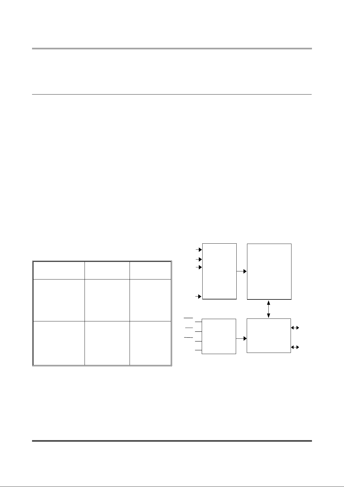
BLOCK DIAGRAM
DECODER
A0
A16
I/O8
Vcc
.
.
.
.
.
.
DATA I/O
CORE
ARRAY
Vss
I/O1
WE
OE
CE1
CONTROL
CIRCUIT
CE2
TE
CH
tm
T15M1024A
TM Technology Inc. reserves the right P. 2 Publication Date: FEB. 2002
to change products or specifications without notice. Revision:A
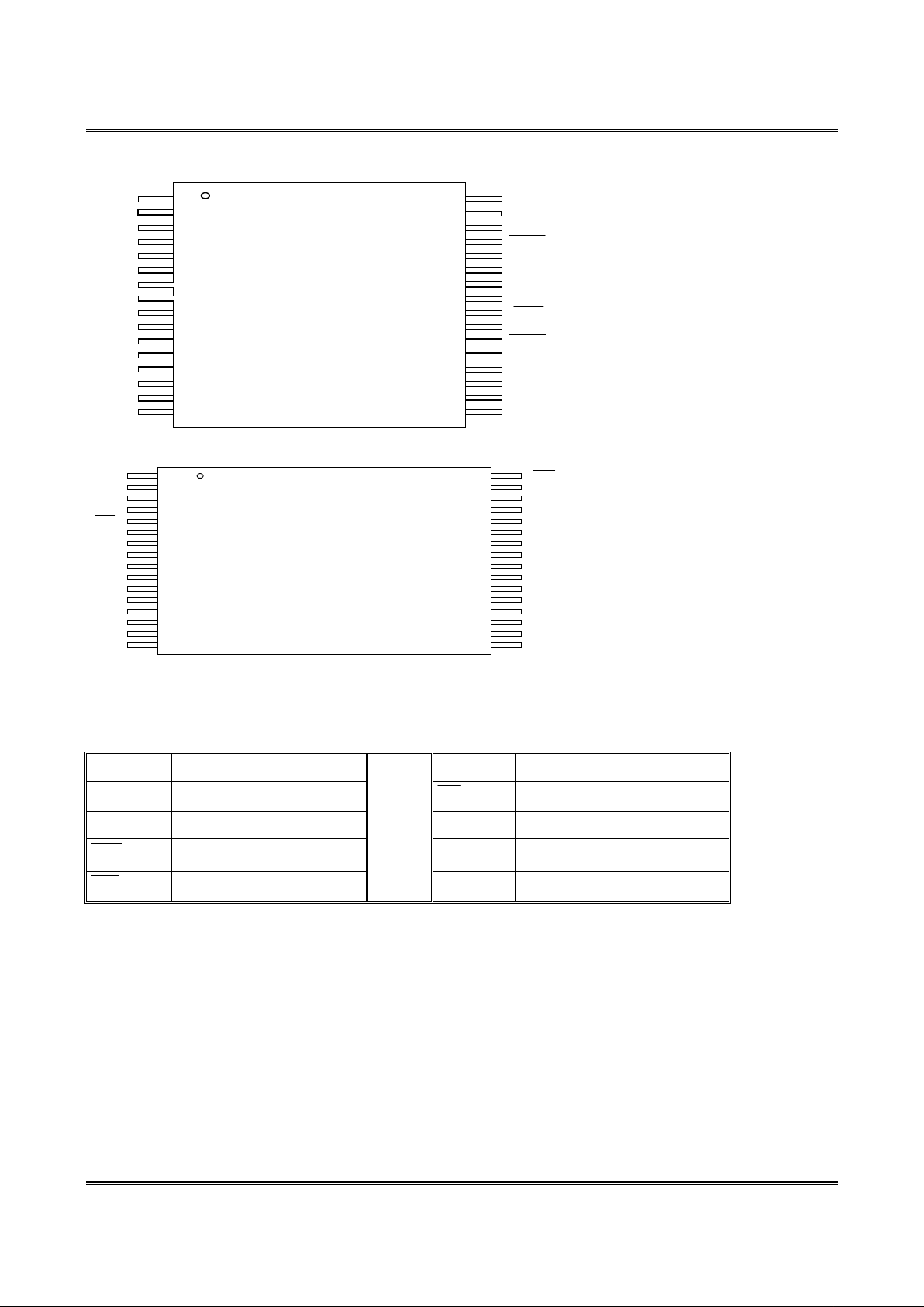
PIN CONFIGURATIONS
DIP
&
SOP
1
2
3
4
5
6
7
8
9
10
11
12
13
14
15
16
32
31
30
29
28
27
26
25
24
23
22
21
20
19
18
17
NC
A16
A14
A12
A7
A6
A5
A4
A3
A2
A1
A0
I/O1
I/O2
I/O3
VSS
VDD
A15
CE2
WE
A13
A8
A9
A11
OE
A10
CE1
I/O8
I/O7
I/O6
I/O5
I/O4
TSOP-I
(8x20mm)
&
(8x13.4mm)
1
2
3
4
5
6
7
8
9
10
11
12
13
14
15
16
32
31
30
29
28
27
26
25
24
23
22
21
20
19
18
17
A11
A9
A8
A13
WE
CE2
A15
VDD
NC
A16
A14
A12
A7
A6
A5
A4
OE
A10
CE1
I/O8
I/O7
I/O6
I/O5
I/O4
VSS
I/O3
I/O2
I/O1
A0
A1
A2
A3
PIN DESCRIPTIONS
SYMBOL DESCRIPTIONS SYMBOL DESCRIPTIONS
A0 ~ A16 Address inputs
OE
Output enable input
I/O1~I/O8 Data inputs/outputs VDD Power supply
CE1
,
CE2
Chip enable VSS Ground
WE
Write enable input
NC No connection
TE
CH
tm
T15M1024A
TM Technology Inc. reserves the right P. 3 Publication Date: FEB. 2002
to change products or specifications without notice. Revision:A
ABSOLUTE MAXIMUM RATINGS*
PARAMETER SYM MIN. MAX. UNIT
Voltage on Any Pin Relative to Gnd VR -0.5 +7 V V
Power Dissipation
P
D
- 0.7 W
Storage Temperature
T
STG
-55 +150 °C
Temperature Under Bias
I
BIAS
0/-40 +70/+85 °C
*Note: Stresses greater than those listed above Absolute Maximum Ratings may cause permanent damage to
the device. This is a stress rating only and function operation of the device at these or any other
conditions outside those indicated in the operational sections of this specification is not implied.
Exposure to absolute maximum rating conditions for extended periods may affect reliability.
TRUTH TABLE
CE 1
CE2
WE
OE
DATA MODE
H X X X High-Z
Standby
X L X X High-Z
Standby
L H H L Data Out Active, Read
L H H H High-Z Active, Output Disable
L H L X Data In Acitve, Write
*Note: X = Don’t Care, L = Low, H = High
TE
CH
tm
T15M1024A
TM Technology Inc. reserves the right P. 4 Publication Date: FEB. 2002
to change products or specifications without notice. Revision:A
OPERATING CHARACTERISTICS
(Vcc = +5V /
±10%
, Gnd = 0V, Ta = 0 ~ +70 °C / -40°C ~ 85°C)
-55 -70 -100
PARAMETER SYM. TEST CONDITIONS
Min Max Min Max Min Max
UNIT
Input Leakage
Current
I
LI
Vcc = Max,
V
IN
= Gnd to Vcc
- 1 - 1 - 1 uA
Output Leakage
Current
I
LO
CE1
= VIH or CE2= VIL
or
OE
= VIH
or
WE
= VIL
V
OUT
= Gnd to Vcc
- 1 - 1 - 1 uA
Operating Power
Supply Current
I
CC
CE1
= VIL,CE2= V
IH,
WE
=V
IH,
OE
= V
IH ,
V
IN
= VIH or V
IL,
I
OUT
=0mA
- 2 - 2 - 2 mA
I
CC1
Cycle time=1us,
100% duty, I
OUT
=0mA,
CE1
≤ 0.2V,
CE2 ≥ V
CC
-0.2V,
V
IN
≤ 0.2V
- 3 - 3 - 3 mA
Average Operating
Current
I
CC2
Cycle time=min,
100% duty, I
OUT
=0mA,
CE1
= VIL,CE2= V
IH ,
V
IN
= VIH or VIL
- 40 - 35 - 25 mA
Standby Power
Supply Current
(TTL Level)
I
SB
CE1
=VIH
CE2= V
IL
- 0.5 - 0.5 - 0.5 mA
0°C
to
70°C
- 15 - 15 - 15
Standby Power
Supply Current
(CMOS Level)
I
SB1
CE1
≥ Vcc-0.2V,
CE2 ≥ V
CC
-0.2V
or CE2 ≤ 0.2V
V
IN
≤ 0.2V or
V
IN
≥ Vcc-0.2V
-40°C
to
85°C
- 20 - 20 - 20
uA
Output Low Voltage
V
OL
IOL= 2.1mA
- 0.4 - 0.4 - 0.4 V
Output High Voltage
V
OH
I
OH
= -1.0 mA
2.4 - 2.4 - 2.4 - V
TE
CH
tm
T15M1024A
TM Technology Inc. reserves the right P. 5 Publication Date: FEB. 2002
to change products or specifications without notice. Revision:A
RECOMMENDED OPERATING CONDITIONS
(Ta = 0 ~ +70 °C /-40°C to 85°C**)
PARAMETER SYM MIN MAX UNIT
Vcc 4.5 5.5 V
Supply Voltage
Gnd 0.0 0.0 V
V
IH
0.6Vcc Vcc+0.3 V
Input Voltage
V
IL
-0.3 0.4 V
CAPACITANCE
(f = 1 MHz, Ta = 25°C,)
PARAMETER SYMBOL CONDITION MAX. UNIT
Input Capacitance
C
IN
V
IN
= 0V
6 pF
Input/ Output Capacitance
C
I/O
V
IN
=
V
OUT
= 0V
8 pF
Note: This parameter is guaranteed by device characterization and is not production tested.
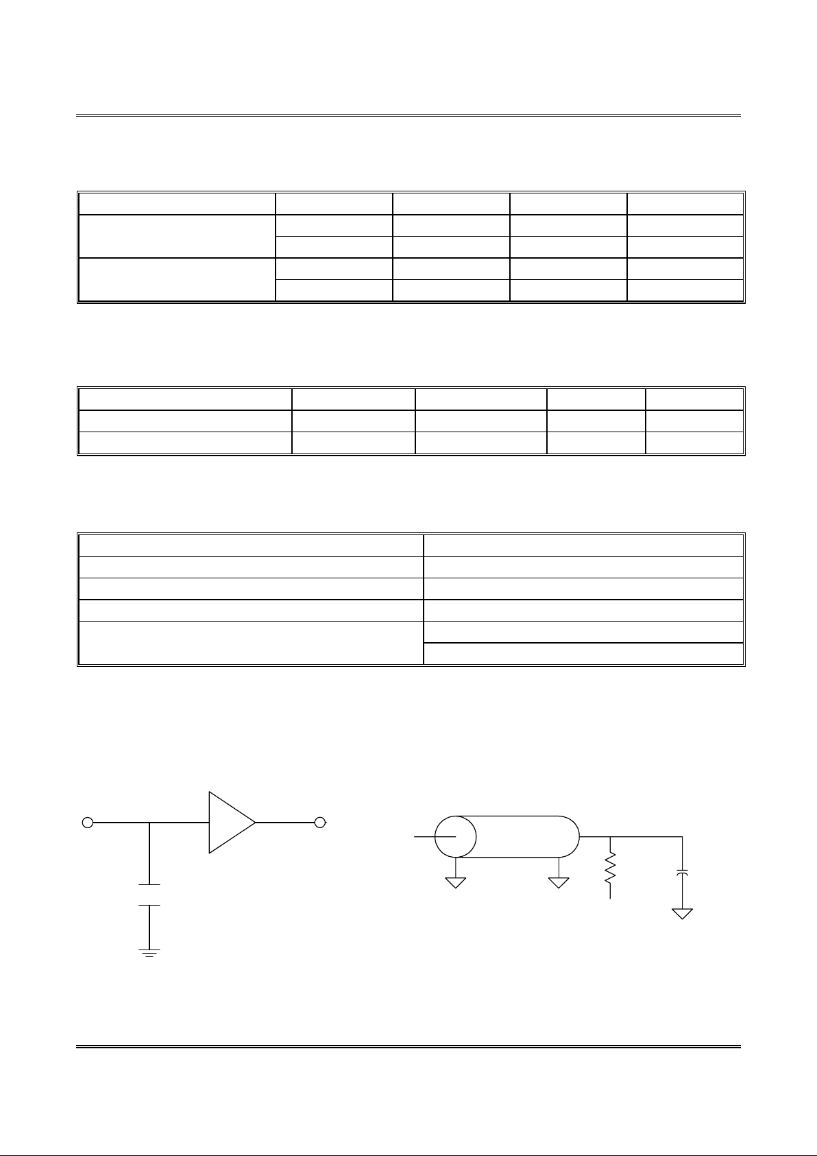
AC TEST CONDITIONS
PARAMETER CONDITIONS
Input Pulse Levels 0.4V to 0.6Vcc
Input Rise and Fall Times 5.0 ns
Input and Output Timing Reference Level 1.5V
C
L
=30pF+1TTL Load(55ns/70ns)
Output Load
C
L
=100pF+1TTL Load(Load for 100ns)
AC TEST LOADS AND WAVEFORM
DQ
Z
0
= 50 ohm
50 ohm
30 pF
Vt =1.5V
Fig.A * Including Scope and Jig Capacitance
TTL
CL*
Fig.B Output Load Equivalent
R
L
C
L

TE
CH
tm
T15M1024A
TM Technology Inc. reserves the right P. 6 Publication Date: FEB. 2002
to change products or specifications without notice. Revision:A
AC CHARACTERISTICS
(
V
cc
= +5V / ±10%, Gnd = 0V, Ta = 0 ~ +70 °C /-40°C to 85°C)
(1) READ CYCLE
-55 -70 -100
PARAMETER SYM.
Min Max Min Max Min Max
UNIT
Read Cycle Time
t
RC
55 - 70 - 100 - ns
Address Access Time
t
AA
- 55 - 70 - 100 ns
Chip Enable Access Time
t
ACE
- 55 - 70 - 100 ns
Output Enable Access Time
t
OE
- 25 - 35 - 50 ns
Output Hold from Address Change
t
OH
10 - 10 - 10 - ns
Chip Enable to Output in Low-Z
t
LZ
10 - 10 - 10 - ns
Chip Disable to Output in High-Z
t
HZ
- 20 - 25 - 30 ns
Output Enable to Output in Low-Z
t
OLZ
5 - 5 - 5 - ns
Output Disable to Output in High-Z
t
OHZ
- 20 - 25 - 30 ns
(2)WRITE CYCLE
-55 -70 -100
PARAMETER SYM.
Min Max Min Max Min Max
UNIT
Write Cycle Time
t
WC
55 - 70 - 100 - ns
Chip Enable to Write End
t
CW
50 - 60 - 80 - ns
Address Valid to Write End
t
AW
50 - 60 - 80 - ns
Address Setup Time
t
AS
0 - 0 - 0 - ns
Write Pulse Width
t
WP
45 - 50 - 70 - ns
Write Recovery Time
t
WR
0 - 0 - 0 - ns
Data Valid to Write End
t
DW
25 - 30 - 40 - ns
Data Hold Time
t
DH
0 - 0 - 0 - ns
Write Enable to Output in High-Z
t
WHZ
- 25 - 25 - 30 ns
Output Active from Write End
t
OW
5 - 5 - 5 - ns

TE
CH
tm
T15M1024A
TM Technology Inc. reserves the right P. 7 Publication Date: FEB. 2002
to change products or specifications without notice. Revision:A
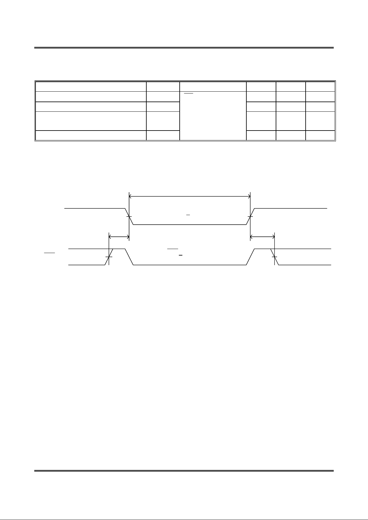
TIMING WAVEFORMS
READ CYCLE 1
(Address Controlled)
READ CYCLE 2
(Chip Enable Controlled)
Notes (READ CYCLE) :
1.
WE
are high for read cycle.
2. All read cycle timing is referenced from the last valid address to the first transition address.
3. t
HZ
and t
OHZ
are defined as the time at which the outputs achieve the open circuit condition referenced to
V
OH
or VOL levels.
4. At any given temperature and voltage condition. t
HZ
(max.) is less than t
LZ
(min.) both for a given device
and from device to device interconnection.
5. Transition is measured ±200mV from steady state voltage with load. This parameter is sampled and not
100% tested.
6. Device is continuously selected with
1CE
=VIL .
DON' T CARE
UNDEFINED
CE1
t
OLZ
CE2
t
ACE
t
OHZ
D
OUT
t
RC
Address
t
OH
t
AA
D
OUT
Previous Data Va lid Data Valid

TE
CH
tm
T15M1024A
TM Technology Inc. reserves the right P. 8 Publication Date: FEB. 2002
to change products or specifications without notice. Revision:A
WRITE CYCLE 1 (
WE
Controlled)
WRITE CYCLE 2 (
CE Controlled)
NOTES ( WRITE CYCLE ) :
1. A write occurs during the overlap of a low
1CE
, a high CE2 and a low WE . A write begins at
the lateat transition among
1CE goes low, CE2 going high and WE going low. A write end at
the earliest transition among
1CE
going high, CE2 going low and WE going high. tWP is
measured from the beginning of write to the end of write.
2. tCW is measured from the later of
1CE going low or CE2 going high to the end of write.
3. tAS is measured from the address valid to the beginning of write.
4. tWR is measured from the end of write to the address change.
t
WC
t
WHZ
t
DW
D
IN
t
DH
t
WR
t
AS
t
WP
Address
CE2
CE1
WE
D
OUT
t
AW
t
CW
t
OW
High-Z
High-Z
DON'T CARE
UNDEFINED
t
WC
t
DW
D
IN
t
DH
t
WR
t
AS
t
WP
t
CW
Address
CE1
WE
D
OUT
CE2
t
AW
High-Z
High-Z High-Z
TE
CH
tm
T15M1024A
TM Technology Inc. reserves the right P. 9 Publication Date: FEB. 2002
to change products or specifications without notice. Revision:A
DATA RETENTION CHARACTERISTICS
PARAMETER SYM. TEST CONDITION MIN. MAX. UNIT
VCC for Data Retention VDR
1CE
≥ V
DD
-0.2V
1.5 - V
Data Retention Current I
CCDR
CE2 ≤ 0.2V - 5* uA
Chip Deselect to Data Retention
Time
t
CDR
VIN ≥ Vcc -0.2V or 0 - ns
Operation Recovery Time tR VIN ≤ 0.2V tRC - ns
* 0 ~ +70 °C / -40 ~ +85 °C,VCC=3V
DATA RETENTION WAVEFORM
(Ta = 0 ~ +70 °C /-40°C to 85°C)
Da ta R ete ntio n Mo de
V
DR
> 1.5V
Vcc_typ
t
CDR
VCC
CE1
V
IH
CE1>V CC-0.2V
V
IH
t
R
Vcc_TYP

TE
CH
tm
T15M1024A
TM Technology Inc. reserves the right P. 10 Publication Date: FEB. 2002
to change products or specifications without notice. Revision:A
PACKAGE DIMENSIONS
32-LEAD SOP
1
16
17
32
EHE
b
D
S
A
A2
A1
Seating Plane
e
y
See De tail F
LE
C
e1
L
e1
Detail F
Dimension in inches Dimension in mm
Symbol
min. typ. max min. typ. max.
A
- - 0.118 - - 3.00
A1
0.004 - - 0.10 - -
A2
0.101 0.106 0.111 2.57 2.69 2.82
b
0.014 0.016 0.020 0.36 0.41 0.51
C
0.006 0.008 0.012 0.15 0.20 0.31
D
- 0.805 0.817 - 20.45 20.75
E
0.440 0.445 0.450 11.18 11.30 11.43
e
0.044 0.050 0.056 1.12 1.27 1.42
HE
0.546 0.556 0.556 13.87 14.12 14.38
L
0.023 0.031 0.039 0.58 0.79 0.99
LE
0.047 0.055 0.063 1.19 1.40 1.60
S
- - 0.036 - - 0.91
y
- - 0.004 - - 0.10
θθθθ
0°
-
10° 0°
-
10°
Notes :
1. Dimensions D max. & S
include mold flash or tie bar
burrs.
2. Dimension b does not include
dambar protrusion / intrusion.
3. Dimensions D & E include
mold mismatch and determined
at the mold parting line.
4. controlling dimension : inches
5. general appearance spec should
be based on final visual
inspection spec.

TE
CH
tm
T15M1024A
TM Technology Inc. reserves the right P. 11 Publication Date: FEB. 2002
to change products or specifications without notice. Revision:A
PACKAGE DIMENSIONS
32-LEAD TSOP (8x20mm)
DIMENSIONS IN INCHES DIMENSIONS IN MM
SYMBOL
MIN NOM MAX MIN NOM MAX
A -- - 0.047 - - 1.20
A1 0.002 - 0.006 0.05 - 0.15
A2 0.035 0.040 0.041 0.90 1.00 1.05
b 0.007 0.008 0.011 0.17 0.20 0.27
C 0.004 0.006 0.008 0.10 0.15 0.21
D 0.787 TYP 20.00 TYP
Db 0.724 TYP 18.40 TYP
E 0.315 TYP 8.00 TYP
L 0.020 0.024 0.028 0.598 0.610 0.622
L1 0.032 TYP 0.813 TYP
θ
0°~12° 0°~12°

TE
CH
tm
T15M1024A
TM Technology Inc. reserves the right P. 12 Publication Date: FEB. 2002
to change products or specifications without notice. Revision:A
PACKAGE DIMENSIONS
32-LEAD TSOP-I (8x13.4mm)
SYMBOL Dimension in inches Dimension in mm
A
0.044(MAX) 1.10(MAX)
A1
0.004±0.002 0.05±0.05
A2
0.041(MAX) 1.02(MAX)
b
0.008±0.004 0.20±0.10
C
0.006±0.001 0.15±0.02
D
0.465±0.008 11.8±0.2
E
0.315±0.004 8.0±0.1
HD
0.528±0.008 13.4±0.2
e
0.020(TYP.) 0.5(TYP.)
L
0.020±0.004 0.5±0.1
L1
0.031±0.008 0.8±0.2
y
0.002(MAX) 0.05(MAX)
θθθθ
0° ~ 5°
0° ~ 5°

TE
CH
tm
T15M1024A
TM Technology Inc. reserves the right P. 13 Publication Date: FEB. 2002
to change products or specifications without notice. Revision:A
PACKAGE DIMENSIONS
32-LEAD DIP (600mil)
1
16
17
32
E
£c
e1
C
A2A1
LA
SEATING PLANE
e
b1 b
D
Dimension in inches Dimension in mm
Symbol
Min Nom Max Min Nom Max
A
- - 0.200 - - 5.08
A1
0.015 - - 0.38 - -
A2
0.142 0.150 0.158 3.61 3.81 4.01
b
0.014 0.018 0.022 0.36 0.46 0.56
b1
0.056 0.060 0.064 1.42 1.52 1.62
C
0.008 0.010 0.014 0.20 0.25 0.35
D
1.642 1.650 1.658 41.71 41.91 42.11
E
0.527 0.535 0.543 13.40 13.60 13.80
e
- 0.100 - - 2.54 -
e1
- 0.600 - - 15.24 -
L
0.118 0.130 0.142 3.00 3.30 3.60
θ
0 ~ 15°
 Loading...