Taitron BSS138 Schematic [ru]

T
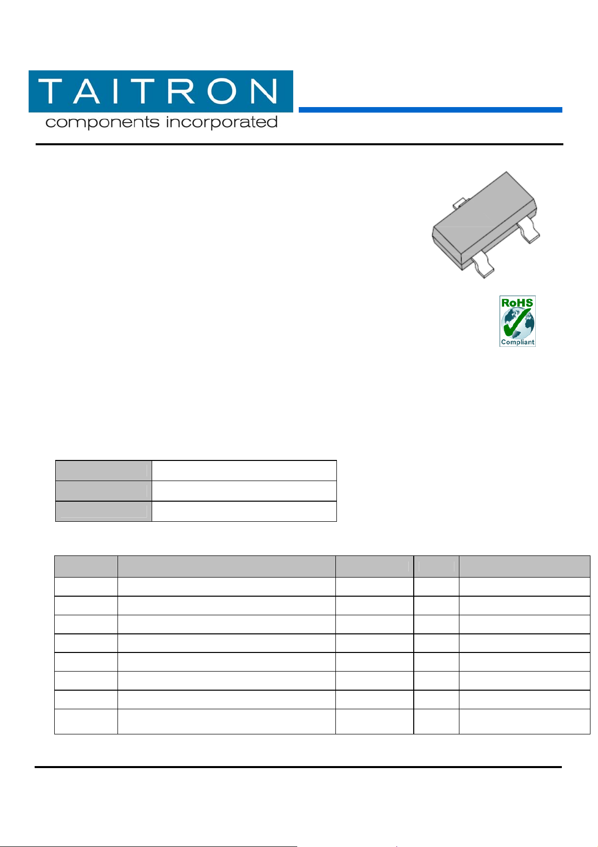
SMD Power MOSFET
Transistor (N-Channel)
SMD Power MOSFET Transistor (N-Channel)
Features
• Low On-Resistance:3.5Ω
• Low input capacitance:40pF
• Low output capacitance:12pF
• Low threshole:1.5V
• Fast switching speed:20nS
• RoHS Compliance
Application
• DC to DC converter
• Cellular & PCMCIA card
• Cordless telephone
• Power management in portable and battery etc.
BSS138
SOT-23
Mechanical Data
Case:
Terminals:
Weight:
Maximum Ratings (T
Symbol Description BSS138 Unit Conditions
VDSS
VGS
ID
IDM
PD
RthJA
TJ,
TSTG
Marking Code J1
Drain-Source Voltage 50 V
Gate-Source Voltage ± 20 V
Drain Current Continuous 200 mA T
Drain Current Pulsed (tp≤10µS) 800 mA
Drain Power Dissipation 225 mW T
Thermal Resistance, Junction to Ambient
Storage Temperature Range
SOT-23, Plastic Package
Solderable per MIL-STD-202G, Method 208
0.008 gram
=25ºC unless noted otherwise)
Ambient
A=25° C
A=25° C
556 ° C/W
-55 to +150 ° C
TAITRON COMPONEN
Tel: (800)-TAITRON (800)-824-8766 (661)-257-6060
Fax: (800)-TAITFAX (800)-824-8329 (661)-257-6415
S INCORPORATED www.taitroncomponents.com
Rev. A/AH
Page 1 of 7

)
SMD Power MOSFET Transistor (N-Channel
BSS138
Electrical Characteristics (T
Symbol Description Min. Typ. Max. Unit Conditions
V(BR)DSS
VGS(th)
IGSS
IDSS
RDS(ON)
gFS
Drain-Source Breakdown Voltage
Gate-Source Threshold Voltage 0.5 - 1.5 V VDS=VGS, ID=1mA
Gate-Source Leakage Current - - ± 0.1 μA V
Zero Gate Voltage Drain Current
Drain-Source On-Resistance
Forward Transconductance
=25ºC unless noted otherwise)
Ambient
50 - - V V
- - 0.1 μA VDS=25V, VGS=0V
- - 0.5 μA V
- 5.6 10 Ω
- - 3.5 Ω V
100 - - mS
GS=0V, ID=250µA
DS=0V, VGS=±20V
DS=50V, VGS=0V
V
GS=2.75V, ID<200mA,
A=-40 to +85 ° C
T
GS=5.0V, ID=200mA
DS=25V, ID=200mA,
V
f=1.0KHz
Dynamic Characteristics
Symbol Description Min. Typ. Max. Unit Conditions
(T
=25ºC unless noted otherwise)
Ambient
Ciss
Crss
Coss
ton
toff
Input Capacitance - 40 50
Reverse Transfer Capacitance - 3.5 5.0
Output Capacitance - 12 25
Switching Time Turn-On Time - - 20
Switching Time Turn-Off Time - - 20
Note: (1) Pulse Test: Pulse Width≤300μs, Duty Cycle≤2%
(2) Switching Time is Essentially Independent of Operating Temperature.
pF
nS V
V
DS=25V, VGS=0V,
f=1MHz
DD=30V, ID=200mA
Rev. A/AH
www.taitroncomponents.com
Page 2 of 7

)
SMD Power MOSFET Transistor (N-Channel
BSS138
Switching Time Test Circuit
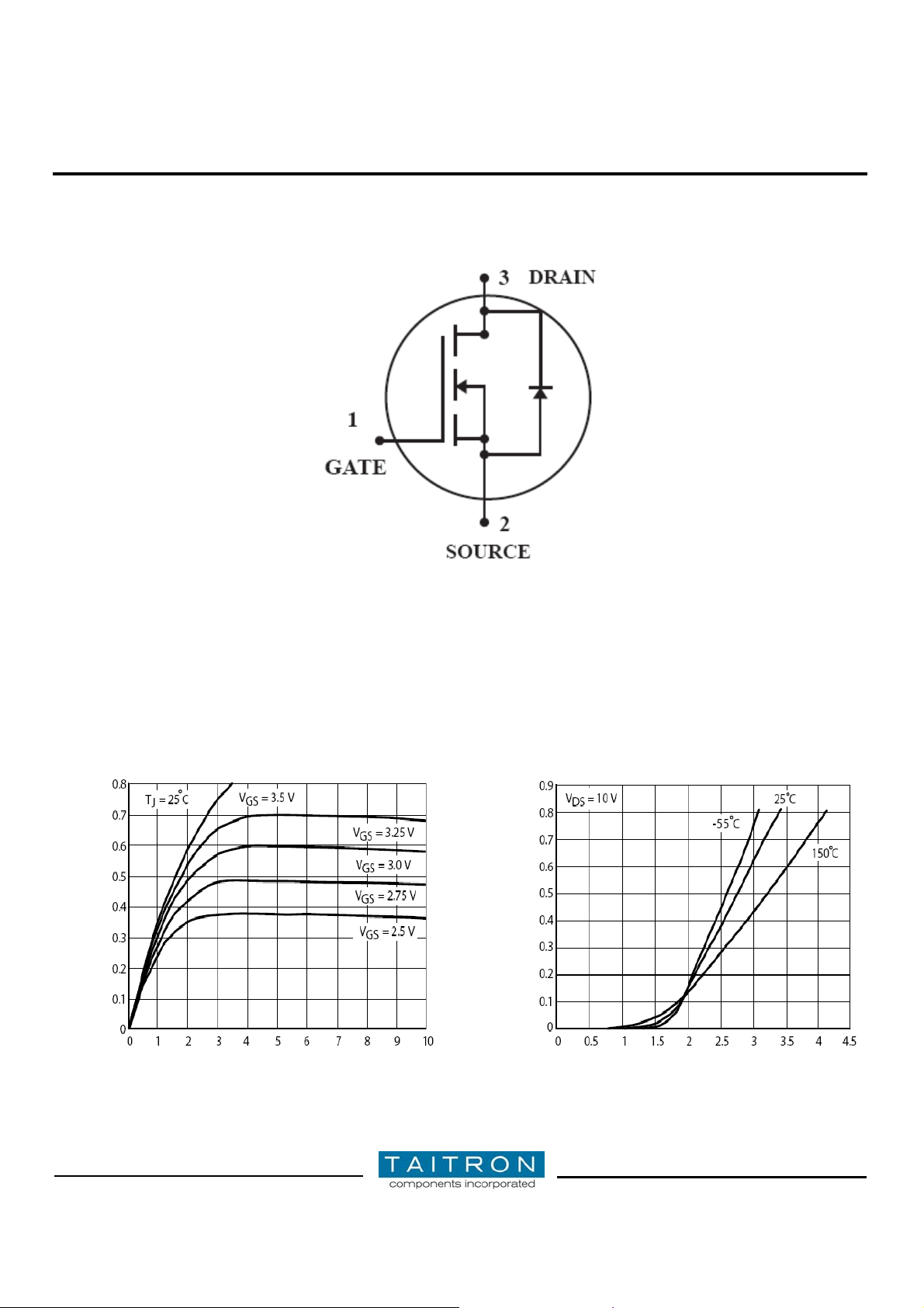
Typical Characteristics Curves
Drain Current ID (A)
Fig.1- On-Region Characteristics
Drain-Source Voltage
VDS (V)
Fig.2- Transfer Characteristics
ID (A)
Drain Current
Gate-Source Voltage
VGS (V)
Rev. A/AH
www.taitroncomponents.com
Page 3 of 7
 Loading...