Rev. A/NX
BAW56WS
Page 1 of 6
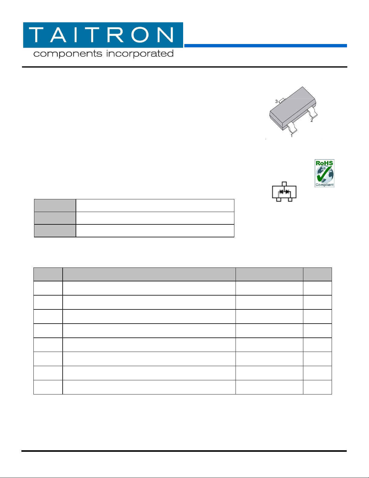
Three Terminals
SMD Switching Diode
Symbol
Description
BAW56
Unit
Marking Code
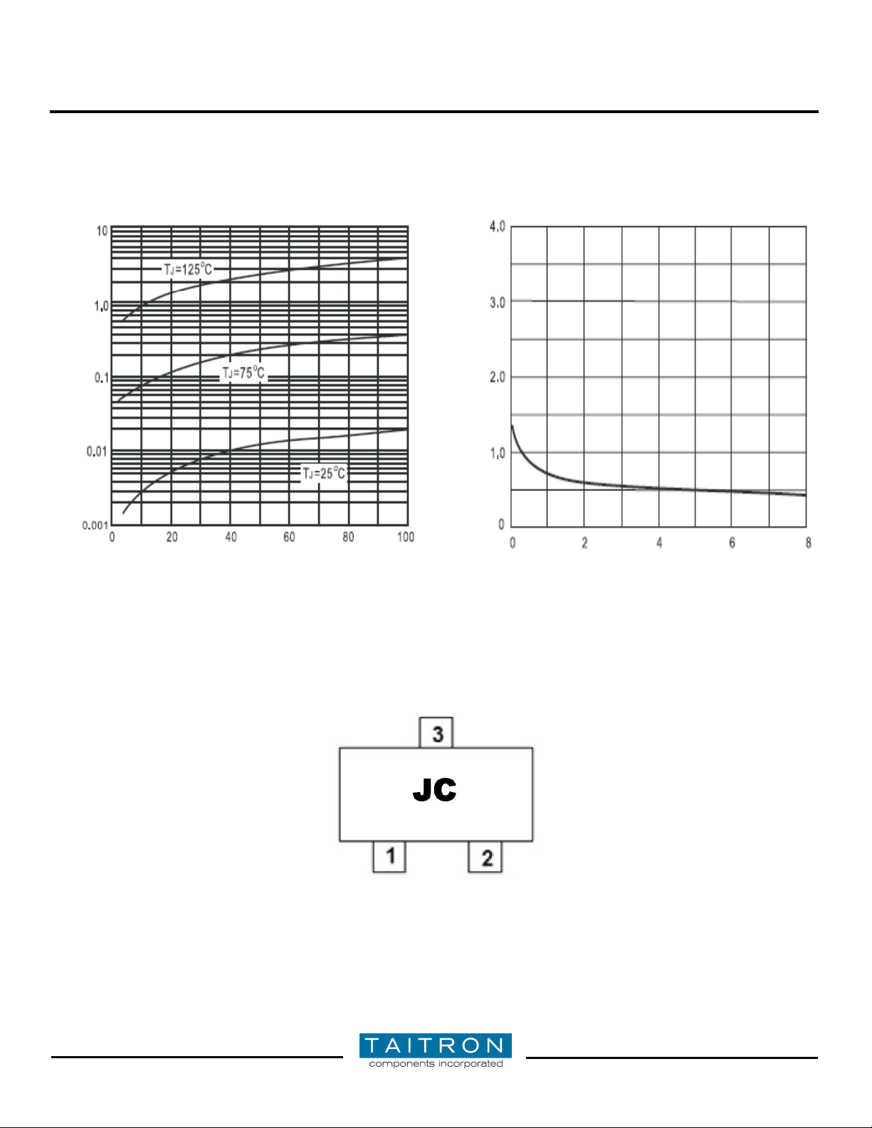
JC
VRM
Reverse Voltage
75
V
VRRM
Peak Reverse Voltage
100
V
IF(AV)
Forward Average Current, Half Wave Rectification with Resistive
Load and f≥50Hz
150
mA
IFSM
Peak Forward Surge Current (0.001mS)
4
A
PD
Power Dissipation Derate above 25° C
200
mW
TJ
Junction Temperature
-55 to +150
° C
TSTG
Storage Temperature Range
-55 to +150
° C
Case:
SOT-323, Plastic Case
Terminals:
Solderable per MIL-STD-750, Method 2026
Weight:
Approx. 0.005 gram
SOT-323
Three Terminals SMD Switching Diode
Features
Fast switching speed
Surface mount package ideally suited for automatic insertion
Electrically Identical to Standard JEDEC
High Conductance
RoHS Compliant
Mechanical Data
Maximum Ratings (T
=25ºC unless noted otherwise)
Ambient

Three Terminals SMD Switching Diode
Rev. A/NX
BAW56WS
www.taitroncomponents.com
Page 2 of 6
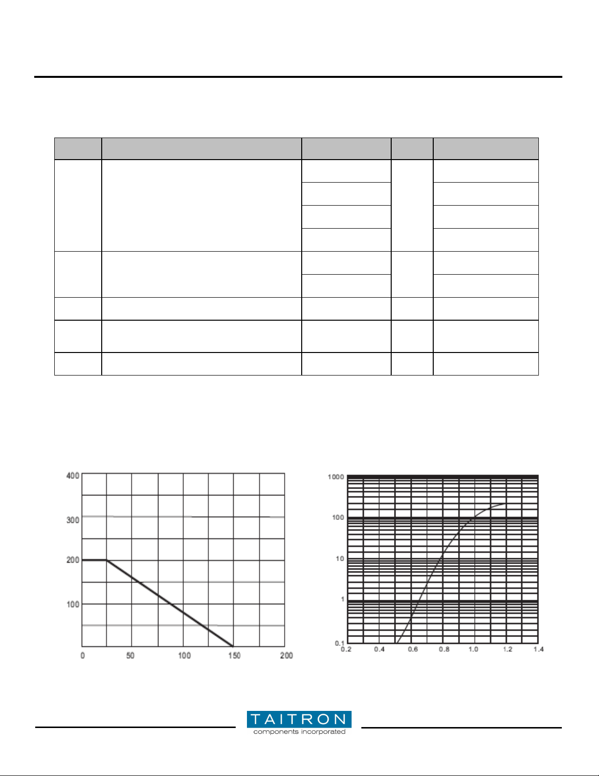
Fig.1- Power Derating Curve
Fig.2- Typical Forward Characteristics
Ambient Temperature (°C )
Forward Voltage (V)
Symbol
Description
BAW56
Unit
Conditions
VF
Forward Voltage
0.715
V
IF=1mA
0.855
IF=10mA
1.0
IF=50mA
1.25
IF=150mA
IR
Reverse Current
0.03
µA
VR=25V
2.5
VR=75V
CT
Total Capacitance
1.5
pF
VR=0V, f=1MHz
Trr
Reverse Recovery Time
4
nS
From IF=10mA to
IR=1mA, VR=6V
RL=100Ω
RthJA
Thermal Resistance from Junction to Ambient
Air
625
° C/W
Forward Current (mA)
Power Dissipation (mW)
Electrical Characteristics (T
=25ºC unless noted otherwise)
Ambient
Typical Characteristics Curves

Three Terminals SMD Switching Diode
Rev. A/NX
BAW56WS
www.taitroncomponents.com
Page 3 of 6
Fig.3- Typical Reverse Characteristics
Reverse Voltage (V)
Reverse Current (µA)
Fig.4- Typical Junction Capacitance
Reverse Voltage (V)
Junction Capacitance (pF)
Marking Information:
 Loading...