

Page 1

Series
3
Technical Reference Manual
980327-02
Page 2

Trademarks
I
P
All rights reserved. This product or document is protected by copyright and distributed under licenses restricting its
use, copying, distribution and decompilation. No part of this product or document may be reproduced in any form
by any means without prior written authorization of Sun and its licensors, if any. This product or the products
depicted herein may be protected by one or more U.S. or international patents or pending patents. Portions of this
product may be derived from the UNIX® and Berkeley 4.3 BSD systems, licensed from UNIX Systems
Laboratories, Inc. and the University of California, respectively. Third party font software in this product is
protected by copyright and licensed from Sun’s Font Suppliers.
RESTRICTED RIGHTS LEGEND: Use, duplication, or disclosure by the government is subject to restrictions as
set forth in subparagraph (c) (1) (ii) of the Rights in Technical Data and Computer Software clause at DFARS
252.227-7013 and FAR 52.227-19.
Sun, Sun Microsystems, the Sun Logo, OpenWindows, SunView, SunOS, DeskSet, NFS and NEWS are trademarks
or registered trademarks of Sun Microsystems, Inc. UNIX and OPEN LOOK are registered trademarks of UNIX
Systems Laboratories, Inc. All other product names mentioned herein are the trademarks of their respective owners.
All SPARC trademarks, including the SCD Compliant Logo, are trademarks or registered trademarks of SPARC
International, Inc. The SPARCbook trademark is licensed exclusively to Tadpole Technology, Inc. Products bearing
SPARC trademarks are based upon an architecture developed by Sun Microsystems, Inc.
The OPEN LOOK® and Sun™ Graphical User Interfaces were developed by Sun Microsystems, Inc. for its users
and licensees. Sun acknowledges the pioneering efforts of Xerox in researching and developing the concept of
visual or graphical user interfaces for the computer industry. Sun holds a non-exclusive license from Xerox to the
Xerox Graphical User Interface, which license also covers Sun’s licensees who implement OPEN LOOK GUI’s and
otherwise comply with Sun’s written license agreements.
The X Window System is a product of the Massachusetts Institute of Technology.
UNIX and OPEN LOOK are registered trademarks of UNIX System Laboratories
PostScript is a trademark of Adobe Systems, Inc
Solaris is a product of Sun Microsystems, Inc
Notebook Computing Environment and NCE are trademarks of Tadpole Technology, Inc.
ssue 2.2 (Draft) of February 10, 1997 © 1996, 1997 by Tadpole Technology
art number 980327-02 Printed in the UK
Page 3

Contents
About This Guide ix
Document Summary . . . . . . . . . . . . . . . . . . . . . . . . . . . . . . . . . . . . . . . . . . . . . . . . . . . . .x
Definitions . . . . . . . . . . . . . . . . . . . . . . . . . . . . . . . . . . . . . . . . . . . . . . . . . . . . . . . . . . . xi
Logic states . . . . . . . . . . . . . . . . . . . . . . . . . . . . . . . . . . . . . . . . . . . . . . . . . . . . . . . . xi
Data entities . . . . . . . . . . . . . . . . . . . . . . . . . . . . . . . . . . . . . . . . . . . . . . . . . . . . . . . xi
Typographical conventions . . . . . . . . . . . . . . . . . . . . . . . . . . . . . . . . . . . . . . . . . . . . . . xi
Key presses, buttons, and field names . . . . . . . . . . . . . . . . . . . . . . . . . . . . . . . . . . . xi
Solaris commands . . . . . . . . . . . . . . . . . . . . . . . . . . . . . . . . . . . . . . . . . . . . . . . . . . xii
Notes, cautions and warnings . . . . . . . . . . . . . . . . . . . . . . . . . . . . . . . . . . . . . . . . . xii
Chapter 1 Architecture Overview
1.1 Introduction . . . . . . . . . . . . . . . . . . . . . . . . . . . . . . . . . . . . . . . . . . . . . . . . . . . . 1-2
1.2 Main Components . . . . . . . . . . . . . . . . . . . . . . . . . . . . . . . . . . . . . . . . . . . . . . . 1-2
1.2.1 Base board . . . . . . . . . . . . . . . . . . . . . . . . . . . . . . . . . . . . . . . . . . . . . . . . . . 1-2
1.2.2 CPU module . . . . . . . . . . . . . . . . . . . . . . . . . . . . . . . . . . . . . . . . . . . . . . . . 1-2
1.2.3 Microcontroller module . . . . . . . . . . . . . . . . . . . . . . . . . . . . . . . . . . . . . . . . 1-3
1.2.4 Main display . . . . . . . . . . . . . . . . . . . . . . . . . . . . . . . . . . . . . . . . . . . . . . . .1-3
1.2.5 Other components . . . . . . . . . . . . . . . . . . . . . . . . . . . . . . . . . . . . . . . . . . . . 1-3
1.3 System Architecture . . . . . . . . . . . . . . . . . . . . . . . . . . . . . . . . . . . . . . . . . . . . . 1-4
1.4 Processor . . . . . . . . . . . . . . . . . . . . . . . . . . . . . . . . . . . . . . . . . . . . . . . . . . . . . . 1-5
1.5 Main System Buses . . . . . . . . . . . . . . . . . . . . . . . . . . . . . . . . . . . . . . . . . . . . . . 1-6
1.5.1 Memory bus . . . . . . . . . . . . . . . . . . . . . . . . . . . . . . . . . . . . . . . . . . . . . . . . . 1-6
1.5.2 SBus . . . . . . . . . . . . . . . . . . . . . . . . . . . . . . . . . . . . . . . . . . . . . . . . . . . . . . . 1-6
1.5.3 Ebus . . . . . . . . . . . . . . . . . . . . . . . . . . . . . . . . . . . . . . . . . . . . . . . . . . . . . . .1-7
1.6 DRAM . . . . . . . . . . . . . . . . . . . . . . . . . . . . . . . . . . . . . . . . . . . . . . . . . . . . . . . . 1-8
1.7 Slow I/O Subsystem . . . . . . . . . . . . . . . . . . . . . . . . . . . . . . . . . . . . . . . . . . . . . 1-9
1.7.1 Serial Channels . . . . . . . . . . . . . . . . . . . . . . . . . . . . . . . . . . . . . . . . . . . . . . 1-9
1.7.2 Counter-Timers . . . . . . . . . . . . . . . . . . . . . . . . . . . . . . . . . . . . . . . . . . . . . . 1-9
1.7.3 Interrupt Controller . . . . . . . . . . . . . . . . . . . . . . . . . . . . . . . . . . . . . . . . . . 1-10
1.7.4 EBus Interface and Controller . . . . . . . . . . . . . . . . . . . . . . . . . . . . . . . . . . 1-10
1.8 Fast I/O Subsystem . . . . . . . . . . . . . . . . . . . . . . . . . . . . . . . . . . . . . . . . . . . . . 1-10
1.8.1 SCSI Controller . . . . . . . . . . . . . . . . . . . . . . . . . . . . . . . . . . . . . . . . . . . . . 1-10
1.8.2 Ethernet Controller . . . . . . . . . . . . . . . . . . . . . . . . . . . . . . . . . . . . . . . . . . 1-11
1.8.3 Parallel Port . . . . . . . . . . . . . . . . . . . . . . . . . . . . . . . . . . . . . . . . . . . . . . . . 1-11
1.8.4 FIFOs and DMA Controller . . . . . . . . . . . . . . . . . . . . . . . . . . . . . . . . . . . 1-11
1.9 Graphics and Video Subsystem . . . . . . . . . . . . . . . . . . . . . . . . . . . . . . . . . . . 1-12
1.9.1 Graphics Controller . . . . . . . . . . . . . . . . . . . . . . . . . . . . . . . . . . . . . . . . . . 1-12
1.9.2 VRAM . . . . . . . . . . . . . . . . . . . . . . . . . . . . . . . . . . . . . . . . . . . . . . . . . . . .1-12
1.9.3 RAMDAC, Panel Driver and Video Clock Generator . . . . . . . . . . . . . . . 1-12
1.10 MK48T08 RTCRAM . . . . . . . . . . . . . . . . . . . . . . . . . . . . . . . . . . . . . . . . . . . 1-13
1.11 ISDN and 16-Bit Audio Controller . . . . . . . . . . . . . . . . . . . . . . . . . . . . . . . . . 1-13
1.12 PCMCIA Controller . . . . . . . . . . . . . . . . . . . . . . . . . . . . . . . . . . . . . . . . . . . . 1-14
iii
Page 4

1.13 Modem Interface . . . . . . . . . . . . . . . . . . . . . . . . . . . . . . . . . . . . . . . . . . . . . . 1-14
1.14 Microcontroller Subsystem . . . . . . . . . . . . . . . . . . . . . . . . . . . . . . . . . . . . . . 1-15
Chapter 2 The SPARC CPU
2.1 SPARC Architecture Overview . . . . . . . . . . . . . . . . . . . . . . . . . . . . . . . . . . . . 2-2
2.2 Integer Unit . . . . . . . . . . . . . . . . . . . . . . . . . . . . . . . . . . . . . . . . . . . . . . . . . . . 2-3
2.2.1 Pipeline . . . . . . . . . . . . . . . . . . . . . . . . . . . . . . . . . . . . . . . . . . . . . . . . . . . . 2-3
2.2.2 Instruction set overview . . . . . . . . . . . . . . . . . . . . . . . . . . . . . . . . . . . . . . . 2-3
2.2.3 Traps and interrupts . . . . . . . . . . . . . . . . . . . . . . . . . . . . . . . . . . . . . . . . . . 2-4
2.2.4 Memory protection . . . . . . . . . . . . . . . . . . . . . . . . . . . . . . . . . . . . . . . . . . . 2-5
2.2.5 IU internal registers . . . . . . . . . . . . . . . . . . . . . . . . . . . . . . . . . . . . . . . . . . 2-5
2.2.6 IU control registers . . . . . . . . . . . . . . . . . . . . . . . . . . . . . . . . . . . . . . . . . . . 2-6
2.3 Floating Point Unit . . . . . . . . . . . . . . . . . . . . . . . . . . . . . . . . . . . . . . . . . . . . . . 2-7
2.3.1 Floating Point Registers . . . . . . . . . . . . . . . . . . . . . . . . . . . . . . . . . . . . . . . 2-8
2.4 Cache Controller and Memory Management Unit . . . . . . . . . . . . . . . . . . . . . . 2-8
2.4.1 Translation lookaside buffer . . . . . . . . . . . . . . . . . . . . . . . . . . . . . . . . . . . . 2-9
2.4.2 Address translation . . . . . . . . . . . . . . . . . . . . . . . . . . . . . . . . . . . . . . . . . . 2-11
2.5 Memory Interface . . . . . . . . . . . . . . . . . . . . . . . . . . . . . . . . . . . . . . . . . . . . . . 2-14
2.6 Instruction Cache . . . . . . . . . . . . . . . . . . . . . . . . . . . . . . . . . . . . . . . . . . . . . . 2-14
2.7 Data Cache . . . . . . . . . . . . . . . . . . . . . . . . . . . . . . . . . . . . . . . . . . . . . . . . . . . 2-14
2.8 SBus Controller . . . . . . . . . . . . . . . . . . . . . . . . . . . . . . . . . . . . . . . . . . . . . . . 2-14
2.8.1 Programmed I/O . . . . . . . . . . . . . . . . . . . . . . . . . . . . . . . . . . . . . . . . . . . . 2-15
2.8.2 DVMA . . . . . . . . . . . . . . . . . . . . . . . . . . . . . . . . . . . . . . . . . . . . . . . . . . . 2-15
Chapter 3 Memory Map and Interrupts
3.1 Address Map . . . . . . . . . . . . . . . . . . . . . . . . . . . . . . . . . . . . . . . . . . . . . . . . . . 3-2
3.1.1 MACIO and SLAVIO Space (SBus Slot 4) . . . . . . . . . . . . . . . . . . . . . . . . 3-2
3.1.2 DRAM . . . . . . . . . . . . . . . . . . . . . . . . . . . . . . . . . . . . . . . . . . . . . . . . . . . . 3-5
3.2 Interrupts . . . . . . . . . . . . . . . . . . . . . . . . . . . . . . . . . . . . . . . . . . . . . . . . . . . . . 3-5
3.2.1 Interrupt Control . . . . . . . . . . . . . . . . . . . . . . . . . . . . . . . . . . . . . . . . . . . . . 3-7
3.3 NCR89C105 SLAVIO Configuration Control . . . . . . . . . . . . . . . . . . . . . . . . . 3-9
3.3.1 SLAVIO Configuration Register . . . . . . . . . . . . . . . . . . . . . . . . . . . . . . . . 3-9
3.3.2 Diagnostic Messages . . . . . . . . . . . . . . . . . . . . . . . . . . . . . . . . . . . . . . . . 3-10
3.3.3 Miscellaneous System Functions . . . . . . . . . . . . . . . . . . . . . . . . . . . . . . . 3-11
Chapter 4 Serial Interface
4.1 Serial Channel Assignment . . . . . . . . . . . . . . . . . . . . . . . . . . . . . . . . . . . . . . . 4-2
4.1.1 Serial Interface Control . . . . . . . . . . . . . . . . . . . . . . . . . . . . . . . . . . . . . . . 4-2
4.2 SCC Registers . . . . . . . . . . . . . . . . . . . . . . . . . . . . . . . . . . . . . . . . . . . . . . . . . 4-3
4.2.1 Register functions . . . . . . . . . . . . . . . . . . . . . . . . . . . . . . . . . . . . . . . . . . . . 4-3
4.3 Baud Rate Clocks . . . . . . . . . . . . . . . . . . . . . . . . . . . . . . . . . . . . . . . . . . . . . . 4-10
4.4 Handshakes . . . . . . . . . . . . . . . . . . . . . . . . . . . . . . . . . . . . . . . . . . . . . . . . . . . 4-10
iv
Page 5

Chapter 5 SCSI Controller
5.1 Connecting SCSI Devices . . . . . . . . . . . . . . . . . . . . . . . . . . . . . . . . . . . . . . . . . 5-2
5.2 NCR53C9X SCSI Controller . . . . . . . . . . . . . . . . . . . . . . . . . . . . . . . . . . . . . . 5-2
5.2.1 53C9X register set . . . . . . . . . . . . . . . . . . . . . . . . . . . . . . . . . . . . . . . . . . . . 5-2
5.3 DMA Support . . . . . . . . . . . . . . . . . . . . . . . . . . . . . . . . . . . . . . . . . . . . . . . . . . 5-7
5.3.1 DMA Transfers . . . . . . . . . . . . . . . . . . . . . . . . . . . . . . . . . . . . . . . . . . . . . . 5-7
5.3.2 DMA Registers . . . . . . . . . . . . . . . . . . . . . . . . . . . . . . . . . . . . . . . . . . . . . . 5-7
5.3.3 SCSI Interrupts . . . . . . . . . . . . . . . . . . . . . . . . . . . . . . . . . . . . . . . . . . . . . . 5-7
Chapter 6 Ethernet Interface
6.1 NCR92C990 Overview . . . . . . . . . . . . . . . . . . . . . . . . . . . . . . . . . . . . . . . . . . . 6-2
6.1.1 Bus Interface . . . . . . . . . . . . . . . . . . . . . . . . . . . . . . . . . . . . . . . . . . . . . . . . 6-2
6.1.2 LAN Interface . . . . . . . . . . . . . . . . . . . . . . . . . . . . . . . . . . . . . . . . . . . . . . . 6-2
6.1.3 Descriptor Management . . . . . . . . . . . . . . . . . . . . . . . . . . . . . . . . . . . . . . . 6-2
6.2 LAN Controller Registers . . . . . . . . . . . . . . . . . . . . . . . . . . . . . . . . . . . . . . . . . 6-3
6.2.1 Register Indexing . . . . . . . . . . . . . . . . . . . . . . . . . . . . . . . . . . . . . . . . . . . . . 6-3
6.2.2 Control and Status Register 0 . . . . . . . . . . . . . . . . . . . . . . . . . . . . . . . . . . . 6-3
6.2.3 Control and Status Register 1 and 2 . . . . . . . . . . . . . . . . . . . . . . . . . . . . . . 6-4
6.2.4 Control and Status Register 3 . . . . . . . . . . . . . . . . . . . . . . . . . . . . . . . . . . . 6-5
6.3 DMA Support for Network Operations . . . . . . . . . . . . . . . . . . . . . . . . . . . . . . . 6-5
Chapter 7 PCMCIA Interface
7.1 TS102 Architecture Overview . . . . . . . . . . . . . . . . . . . . . . . . . . . . . . . . . . . . . 7-2
7.1.1 SBus interface . . . . . . . . . . . . . . . . . . . . . . . . . . . . . . . . . . . . . . . . . . . . . . . 7-2
7.1.2 PCMCIA interface . . . . . . . . . . . . . . . . . . . . . . . . . . . . . . . . . . . . . . . . . . . . 7-3
7.1.3 Microcontroller interface . . . . . . . . . . . . . . . . . . . . . . . . . . . . . . . . . . . . . . . 7-3
7.2 TS102 Memory Mapping . . . . . . . . . . . . . . . . . . . . . . . . . . . . . . . . . . . . . . . . . 7-4
7.2.1 Acceses to PCMCIA Resources . . . . . . . . . . . . . . . . . . . . . . . . . . . . . . . . . 7-4
7.2.2 Byte Swapping . . . . . . . . . . . . . . . . . . . . . . . . . . . . . . . . . . . . . . . . . . . . . . . 7-5
7.2.3 SLAVIO expansion interface . . . . . . . . . . . . . . . . . . . . . . . . . . . . . . . . . . . 7-6
7.3 TS102 Registers . . . . . . . . . . . . . . . . . . . . . . . . . . . . . . . . . . . . . . . . . . . . . . . . 7-7
7.3.1 Card A and B interrupt registers . . . . . . . . . . . . . . . . . . . . . . . . . . . . . . . . . 7-8
7.3.2 Card status register . . . . . . . . . . . . . . . . . . . . . . . . . . . . . . . . . . . . . . . . . . . 7-9
7.3.3 Card Control Register . . . . . . . . . . . . . . . . . . . . . . . . . . . . . . . . . . . . . . . . 7-11
7.3.4 Microcontroller Interrupt Register . . . . . . . . . . . . . . . . . . . . . . . . . . . . . . 7-12
7.3.5 Microcontroller data register . . . . . . . . . . . . . . . . . . . . . . . . . . . . . . . . . . . 7-12
7.3.6 Microcontroller status register . . . . . . . . . . . . . . . . . . . . . . . . . . . . . . . . . . 7-12
7.4 Microcontroller Registers . . . . . . . . . . . . . . . . . . . . . . . . . . . . . . . . . . . . . . . . 7-12
Chapter 8 ISDN and 16-bit Audio
8.1 ISDN Overview . . . . . . . . . . . . . . . . . . . . . . . . . . . . . . . . . . . . . . . . . . . . . . . . . 8-2
8.2 DBRI Overview . . . . . . . . . . . . . . . . . . . . . . . . . . . . . . . . . . . . . . . . . . . . . . . . 8-2
8.2.1 TE and NT Ports . . . . . . . . . . . . . . . . . . . . . . . . . . . . . . . . . . . . . . . . . . . . . 8-3
8.2.2 CHI Port . . . . . . . . . . . . . . . . . . . . . . . . . . . . . . . . . . . . . . . . . . . . . . . . . . . . 8-3
v
Page 6

8.2.3 SBus Interface . . . . . . . . . . . . . . . . . . . . . . . . . . . . . . . . . . . . . . . . . . . . . . . 8-3
8.2.4 DBRI Programming Model . . . . . . . . . . . . . . . . . . . . . . . . . . . . . . . . . . . . 8-4
8.2.5 DBRI Internal Registers . . . . . . . . . . . . . . . . . . . . . . . . . . . . . . . . . . . . . . . 8-7
8.2.6 DBRI Commands . . . . . . . . . . . . . . . . . . . . . . . . . . . . . . . . . . . . . . . . . . . 8-11
8.2.7 Data structures . . . . . . . . . . . . . . . . . . . . . . . . . . . . . . . . . . . . . . . . . . . . . 8-13
8.3 Audio CODEC . . . . . . . . . . . . . . . . . . . . . . . . . . . . . . . . . . . . . . . . . . . . . . . . 8-14
8.3.1 Clocking and Data Synchronization . . . . . . . . . . . . . . . . . . . . . . . . . . . . . 8-14
8.3.2 Control Mode . . . . . . . . . . . . . . . . . . . . . . . . . . . . . . . . . . . . . . . . . . . . . . 8-17
8.3.3 Data Mode . . . . . . . . . . . . . . . . . . . . . . . . . . . . . . . . . . . . . . . . . . . . . . . . 8-20
Chapter 9 MODEM
9.1 Internal Modem Overview . . . . . . . . . . . . . . . . . . . . . . . . . . . . . . . . . . . . . . . . 9-2
9.2 Interface Control . . . . . . . . . . . . . . . . . . . . . . . . . . . . . . . . . . . . . . . . . . . . . . . 9-2
9.3 Modem Registers . . . . . . . . . . . . . . . . . . . . . . . . . . . . . . . . . . . . . . . . . . . . . . . 9-4
9.3.1 Interrupt Enable Register . . . . . . . . . . . . . . . . . . . . . . . . . . . . . . . . . . . . . . 9-4
9.3.2 Interrupt Identification Register . . . . . . . . . . . . . . . . . . . . . . . . . . . . . . . . . 9-4
9.3.3 Line Status Register . . . . . . . . . . . . . . . . . . . . . . . . . . . . . . . . . . . . . . . . . . 9-5
9.4 AT Command Set . . . . . . . . . . . . . . . . . . . . . . . . . . . . . . . . . . . . . . . . . . . . . . . 9-5
9.5 S Registers . . . . . . . . . . . . . . . . . . . . . . . . . . . . . . . . . . . . . . . . . . . . . . . . . . . 9-11
9.6 Class 2 Fax Command Set . . . . . . . . . . . . . . . . . . . . . . . . . . . . . . . . . . . . . . . 9-27
Chapter 10 Parallel Interface
10.1 Parallel Port Overview . . . . . . . . . . . . . . . . . . . . . . . . . . . . . . . . . . . . . . . . . . 10-2
10.1.1 Parallel Port DMA Operations . . . . . . . . . . . . . . . . . . . . . . . . . . . . . . . . . 10-2
10.2 Parallel Port Control Registers . . . . . . . . . . . . . . . . . . . . . . . . . . . . . . . . . . . . 10-3
Chapter 11 Display Interface
11.1 Display Interface Overview . . . . . . . . . . . . . . . . . . . . . . . . . . . . . . . . . . . . . . 11-2
11.1.1 Architecture . . . . . . . . . . . . . . . . . . . . . . . . . . . . . . . . . . . . . . . . . . . . . . . 11-2
11.1.2 Display Interface Timing . . . . . . . . . . . . . . . . . . . . . . . . . . . . . . . . . . . . . 11-3
11.1.3 LCD Power . . . . . . . . . . . . . . . . . . . . . . . . . . . . . . . . . . . . . . . . . . . . . . . . 11-4
11.2 Power 9100 User Interface Controller . . . . . . . . . . . . . . . . . . . . . . . . . . . . . . 11-5
11.2.1 Parameter engine . . . . . . . . . . . . . . . . . . . . . . . . . . . . . . . . . . . . . . . . . . . 11-6
11.2.2 Drawing engine . . . . . . . . . . . . . . . . . . . . . . . . . . . . . . . . . . . . . . . . . . . . . 11-6
11.2.3 Frame buffer controller . . . . . . . . . . . . . . . . . . . . . . . . . . . . . . . . . . . . . . . 11-6
11.2.4 SVGA unit . . . . . . . . . . . . . . . . . . . . . . . . . . . . . . . . . . . . . . . . . . . . . . . . 11-7
11.2.5 Power 9100 host interface . . . . . . . . . . . . . . . . . . . . . . . . . . . . . . . . . . . . 11-7
11.2.6 System Control Registers . . . . . . . . . . . . . . . . . . . . . . . . . . . . . . . . . . . . . 11-9
11.2.7 Video Control Registers . . . . . . . . . . . . . . . . . . . . . . . . . . . . . . . . . . . . . 11-12
11.2.8 VRAM control registers . . . . . . . . . . . . . . . . . . . . . . . . . . . . . . . . . . . . . 11-15
11.2.9 Parameter engine registers . . . . . . . . . . . . . . . . . . . . . . . . . . . . . . . . . . . 11-15
11.2.10Drawing engine registers . . . . . . . . . . . . . . . . . . . . . . . . . . . . . . . . . . . . 11-18
11.2.11RAMDAC register accesses . . . . . . . . . . . . . . . . . . . . . . . . . . . . . . . . . 11-20
11.3 Direct frame buffer access . . . . . . . . . . . . . . . . . . . . . . . . . . . . . . . . . . . . . . 11-20
vi
Page 7

11.4 RAMDAC . . . . . . . . . . . . . . . . . . . . . . . . . . . . . . . . . . . . . . . . . . . . . . . . . . . 11-21
11.4.1 RAMDAC host interface . . . . . . . . . . . . . . . . . . . . . . . . . . . . . . . . . . . . . 11-22
11.4.2 Control register accesses . . . . . . . . . . . . . . . . . . . . . . . . . . . . . . . . . . . . . 11-22
11.4.3 Color palette accesses . . . . . . . . . . . . . . . . . . . . . . . . . . . . . . . . . . . . . . . 11-28
11.4.4 Pixel Formats . . . . . . . . . . . . . . . . . . . . . . . . . . . . . . . . . . . . . . . . . . . . . . 11-29
Chapter 12 Microcontroller Subsystem
12.1 Microcontroller subsystem overview . . . . . . . . . . . . . . . . . . . . . . . . . . . . . . . 12-2
12.1.1 Normal operation . . . . . . . . . . . . . . . . . . . . . . . . . . . . . . . . . . . . . . . . . . . . 12-3
12.1.2 Internal keyboard scanning . . . . . . . . . . . . . . . . . . . . . . . . . . . . . . . . . . . . 12-4
12.1.3 External keyboard and mouse . . . . . . . . . . . . . . . . . . . . . . . . . . . . . . . . . . 12-4
12.1.4 Pointing stick . . . . . . . . . . . . . . . . . . . . . . . . . . . . . . . . . . . . . . . . . . . . . . . 12-4
12.1.5 Real time clock . . . . . . . . . . . . . . . . . . . . . . . . . . . . . . . . . . . . . . . . . . . . . 12-4
12.1.6 EEPROM . . . . . . . . . . . . . . . . . . . . . . . . . . . . . . . . . . . . . . . . . . . . . . . . . . 12-4
12.1.7 LCD status display . . . . . . . . . . . . . . . . . . . . . . . . . . . . . . . . . . . . . . . . . . 12-5
12.2 Command Set . . . . . . . . . . . . . . . . . . . . . . . . . . . . . . . . . . . . . . . . . . . . . . . . . 12-6
12.2.1 Command synchronization . . . . . . . . . . . . . . . . . . . . . . . . . . . . . . . . . . . . 12-6
12.2.2 System Information Commands . . . . . . . . . . . . . . . . . . . . . . . . . . . . . . . . 12-6
12.2.3 Read/Write/Modify Commands . . . . . . . . . . . . . . . . . . . . . . . . . . . . . . . 12-11
12.2.4 Commands Returning no Status . . . . . . . . . . . . . . . . . . . . . . . . . . . . . . . 12-14
12.2.5 Block Transfer Commands . . . . . . . . . . . . . . . . . . . . . . . . . . . . . . . . . . . 12-15
12.2.6 Generic Commands . . . . . . . . . . . . . . . . . . . . . . . . . . . . . . . . . . . . . . . . . 12-16
12.2.7 Generic Commands with Optional Status . . . . . . . . . . . . . . . . . . . . . . . . 12-17
12.2.8 Administration Commands . . . . . . . . . . . . . . . . . . . . . . . . . . . . . . . . . . . 12-18
Appendix A Further Information
Appendix B Connector Information
B.1 I/O Panel Connectors . . . . . . . . . . . . . . . . . . . . . . . . . . . . . . . . . . . . . . . . . . . .B-2
B.1.1 DCIn . . . . . . . . . . . . . . . . . . . . . . . . . . . . . . . . . . . . . . . . . . . . . . . . . . . . . .B-2
B.1.2 Parallel (S3XP, S3GX and S3TX) . . . . . . . . . . . . . . . . . . . . . . . . . . . . . . . .B-2
B.1.3 Parallel (S3 and S3LC) . . . . . . . . . . . . . . . . . . . . . . . . . . . . . . . . . . . . . . . .B-3
B.1.4 Ethernet (S3XP, S3GX and S3TX) . . . . . . . . . . . . . . . . . . . . . . . . . . . . . . .B-3
B.1.5 Ethernet (S3 and S3LC) . . . . . . . . . . . . . . . . . . . . . . . . . . . . . . . . . . . . . . . .B-4
B.1.6 Video . . . . . . . . . . . . . . . . . . . . . . . . . . . . . . . . . . . . . . . . . . . . . . . . . . . . . .B-4
B.1.7 SCSI (S3XP, S3GX and S3TX) . . . . . . . . . . . . . . . . . . . . . . . . . . . . . . . . .B-5
B.1.8 SCSI (S3 and S3LC) . . . . . . . . . . . . . . . . . . . . . . . . . . . . . . . . . . . . . . . . . .B-6
B.1.9 Keyboard/Mouse . . . . . . . . . . . . . . . . . . . . . . . . . . . . . . . . . . . . . . . . . . . . .B-6
B.1.10Serial (x2) . . . . . . . . . . . . . . . . . . . . . . . . . . . . . . . . . . . . . . . . . . . . . . . . . .B-6
B.1.11ISDN . . . . . . . . . . . . . . . . . . . . . . . . . . . . . . . . . . . . . . . . . . . . . . . . . . . . . .B-7
B.2 Cable Adapter Connectors . . . . . . . . . . . . . . . . . . . . . . . . . . . . . . . . . . . . . . . .B-8
B.2.1 Parallel Cable Adapter . . . . . . . . . . . . . . . . . . . . . . . . . . . . . . . . . . . . . . . . .B-8
B.3 Removable Hard Drive SCSI Connector . . . . . . . . . . . . . . . . . . . . . . . . . . . . .B-9
vii
Page 8

viii
Page 9

Note
About This Guide
The SPARCbook 3 Technical Reference Manual is
written for the hardware engineer wishing to carry
out service or repairs, and at the software engineer
wishing to implement hardware drivers. It is
assumed that you are familiar with the operation of
SPARCbook 3, as detailed in the SPARCbook 3
User Guide, and that you have an understanding of
computer hardware.
The SPARCbook 3 Technical Reference Manual covers all
models of SPARCbook 3. Where information for one model
differs to information for another model, this is indicated in the
text.
Page 10

Document Summary
The SPARCbook 3 Technical Reference Manual comprises the following
chapters:
• Chapter 1 ,
SPARCbook 3 and introduces the main hardware devices that provide
control over the SPARCbook 3’s operations. The internal architecture
of SPARCbook 3 is described, showing how the major devices are
connected together.
• Chapter 2,
processor.
• Chapter 3,
architecture and the interrupt architecture of the SPARCbook 3.
• Chapter 4 ,
SPARCbook 3.
• Chapter 5,
• Chapter 6,
SPARCbook 3.
• Chapter 7,
the SPARCbook 3.
• Chapter 8,
16-bit audio controller.
• Chapter 9,
3.
Architecture Overview,
Microprocessor
Memory Map and Interrupts
Serial Interface
SCSI Communications,
Ethernet Interfac
PCMCIA
ISDN and 16-Bit Audio Controller
Modem
, discusses the internal modem on the SPARCbook
, provides an overview of the SPARC
, discusses the serial interface of the
, discusses the PCMCIA interface implemented in
discusses the main features of the
, describes the addressing
discusses the SCSI controller.
e, discusses the Ethernet interface of the
, discusses the ISDN and
• Chapter 10,
SPARCbook 3.
• Chapter 11,
implemented in the SPARCbook 3. The discussion is centered on the
Brooktree Bt445 RAMDAC, on which the interface is based.
• Chapter 12,
subsystem. This is used to provide internal control over such things as
the display brightness, keyboard and mouse scanning and power
management.
x
Parallel Interface
Display Interface
Microcontroller Subsystem
, discusses the parallel interface on the
, discusses the display interface
, discusses the microcontroller
Page 11

Definitions
Logic states
The following conventions are used in the SPARCbook 3 Technical
Reference Manual:
The terms
level ‘0’.
The terms
level ‘1’.
The term
regardless of whether that state is high or low.
The term
regardless of whether that state is high or low.
clear
or
set
or
asserted
negated
low
high
indicates that a signal is in its true or active state
indicates that a signal is in its false or inactive state
Data entities
A
halfword
A
word
A
doubleword
is taken to contain 16 bits.
is taken to contain 32 bits.
is taken to contain 64 bits
Typographical conventions
Different typography is used in this guide to distinguish between normal
text, examples of SPARCbook responses, and cases where you are required
to provide input using the keyboard or mouse.
Key presses, buttons, and field names
Key presses are shown in
you need to press two or more keys; for example:
To switch off your SPARCbook, press
indicate that the signal being discussed is at the logic
indicate that the signal being discussed is at the logic
Helvetica bold
. In order to perform certain tasks,
Pause-O.
In this case, you should press the
holding the
Buttons and field names are also shown in
Click the
Type the name of the file that you want to send in the
key down, press the O key.
Pause
Transmit
button.
key down first, and then, while
Pause
Helvetica bold
. For example:
File Name
field.
xi
Page 12

Solaris commands
Information displayed on your SPARCbook screen by the Solaris
Operating System is shown in
Courier
font.
Courier
is also used to
describe system utilities and commands. For example:
The
mail
system will inform you when there is incoming mail from
another user.
you have mail
Bold Courier
perform a specific task. For example:
To report the current time and date you should use the
command:
%
Notes, cautions and warnings
Notes are used throughout this manual to explain items of related interest
to the topic under discussion, and are used to refer the reader to another part
of the manual, or to other documentation.
Note
This is an example of a note, used as to provide additional information.
Cautions are used to advise the reader of actions that if carried out may
cause damage to the SPARCbook 3.
Caution
This is an example of a caution
Warnings are used to draw your attention to actions that could cause
personal injury or pose a hazard to life. For example:
WARNING!
THE AC ADAPTER SUPPLIED WITH YOUR SPARCBOOK 3 CONTAINS
HAZARDOUS VOLTAGES. IT CONTAINS NO USER SERVICEABLE
PARTS. DO NOT REMOVE THE COVERS.
is used in examples to show what you must type in order to
date
date
xii
Page 13

Architecture Overview
This chapter discusses the architecture of the
SPARCbook 3. It describes the main system
components and how they are packaged together to
deliver workstation-class performance in a compact
notebook form factor.
1
1
Page 14

1.1 Introduction
At the heart of the SPARCbook 3 design concept is the Tadpole Advanced
Notebook Architecture (ANA). This defines a set of goals and guidelines to
which the SPARCbook 3 range of systems are designed. It is a modular
approach which results in a system that implements highly integrated
components to provide the performance and I/O facilities normally
associated with desktop workstations. It also results in a system that can be
readily upgraded by the user with larger memory (up to 128 MB) or disk
capacities or returned to the factory for upgrades with the fastest CPUs
available for notebook implementation.
1.2 Main Components
The SPARCbook 3 contains three printed circuit boards. These are the
S3-XP Base board, the S3-XP or the S3TX CPU module, and the
microcontroller board.
1.2.1 Base board
The S3-XP Base board carries all of the I/O components together with the
display controller, RAMDAC and 2MB of Video RAM, and the battery
management hardware. It is populated on both sides using mainly surface
mount devices in order to keep its physical dimensions to a minimum. The
Base board also carries two PCMCIA sockets and the I/O panel which is
visible at the rear of the assembled system.
Introduction
1.2.2 CPU module
1-2
Architecture Overview
The Base board provides mounting points and sockets to accommodate the
CPU module.
The CPU module carries the main SPARC CPU. The CPU module is
extended to carry the main memory SIMMS. This physical arrangement
has the advantage of making the SIMMs very easy to fit to or remove from
a fully assembled system through the battery tray without the use of tools.
The CPU module is mounted onto the base board such that the CPU itself
is sandwiched between the CPU module and Base board. However, an
interesting feature of the Base board is a large hole through which a
heatsink fitted to the main CPU is allowed to protrude when the two boards
Page 15

Main Components
are fixed together. When the two boards are correctly assembled, the CPU
heatsink is brought into contact with the system’s magnesium base casting
to provide effective heat dissipation, as shown in Figure 1-1.
Figure 1-1 CPU Heat Dissipation
1.2.3 Microcontroller module
The microcontroller module is a small board which carries an Hitachi H8
microcontroller, the status display which is visible from the outside of the
assembled system, and a number of programmable memory devices. It
provides connections for the keyboard and pointing stick for which it
provides control and for the Base board for which it provides system
control and status monitoring functions.
Inter-Board Connectors
Heatsink
CPU
CPU Module
Base Board
System’s Magnesium
Base
1.2.4 Main display
The main display is housed within the system’s lid along with an inverter
board required to drive the display’s backlight. Systems use either 9.4 inch
640 x 480 or 10.4 inch 800 x 600 color TFT display to provide a sharp
image in a wide range of lighting conditions. The brightness of the
backlight is controlled by the microcontroller and can be varied to suit the
lighting conditions or can be dimmed or turned off when required to
conserve battery power.
1.2.5 Other components
In addition to the main boards and display, the SPARCbook 3 system
contains is a 2.5 inch 1.2 GB (or larger when available) SCSI hard disk
drive assembled within a removable module. The drive can be removed
from the SPARCbook 3 while the system is fully assembled, see your
SPARCbook 3 User Guide
.
Architecture Overview
1-3
Page 16

1.3 System Architecture
The SPARCbook 3 system architecture is illustrated in Figure 1-2.
System Architecture
TFT
Display
Ext.
Display
RAMDAC
Graphics
Controller
Microcontroller
Subsystem
Module
Modem
Modem
CPU
Base
Board
Ext.
Keyboard/Mouse
Serial
SLAVIO
SPARC CPU
SCSI
SBus
TS102
ASIC
Ethernet
Parallel
MACIO
Audio
ISDN
ISDN/
Audio
32
2x
PCMCIA
Sockets
Figure 1-2 SPARCbook 3 Architecture
1-4
Architecture Overview
Memory
Bus
DRAM (2 x SIMMs)
64
Page 17

Processor
1.4 Processor
The CPU used in the S3TX is the TurboSPARC and the CPU used in the
S3XPand S3GX is the microSPARC II.
The TurboSPARC CPU provides the following key features:
• SPARC compliant V8 Integer Unit core
• SPARC Reference Memory Management Unit
• Floating Point ALU
• FP-Muliply Unit
• FP Divide/Square Root Unit
• 16 Kbyte Instruction Cache
• 16 Kbyte Data Cache
• Secondary Cache Controller
• DRAM Controller
• SBus Controller, Master and Slave Interface.
The TurboSPARC implemented in the S3TX operates at 170 MHz and
provides performance figures of 3.5 SPECint95 and 3.0 SPECfp95.
The microSPARC II CPU provides the following key features:
• SPARC-II compliant V8 Integer Unit (IU) core
• SPARC Reference Memory Management Unit (MMU)
• MEIKO Floating Point Unit (FPU)
• 16 Kbyte Instruction Cache
• 8 Kbyte Data Cache
• Memory Controller
• SBus Controller, Master & Slave Interface.
The microSPARC II implemented in the SPARCbook 3XP processor
operates at 85 MHz and provides performance figures of 64 SPECint92 and
54.6 SPECfp92.
The microSPARC II implemented in the SPARCbook 3GX processor
operates at 105 MHz and provides performance figures of 64 SPECint92
and 54.6 SPECfp92.
Architecture Overview
1-5
Page 18

1.5 Main System Buses
The SPARCbook 3 architecture is based around three main buses
conventional for SPARC-based workstations. These are the Memory bus
which connects the CPU to the main memory; the SBus which connects the
CPU to the major I/O devices; and the EBus.
1.5.1 Memory bus
The microSPARC II’s integral memory controller is connected to the
system DRAM directly via a 64 bit high speed memory bus. The
microSPARC II provides direct addressing and control for the main
memory, illustrated in Figure 1-3, providing the write enable signal and
RAS and CAS lines. The smallest data movement is 64 bits; smaller
transfers are carried out by using read-modify-write operations. Parity
protection is provided by the CPU as 1 bit per word (32 bits) of data. SBus
based master I/O devices are able to access the memory bus via the
processor’s SBus interface.
Main System Buses
STSX1012
microSPARC II
Figure 1-3 Main Memory/CPU Interface
1.5.2 SBus
The microSPARC II incorporates a complete SBus controller. The SBus
connects the microSPARC II to the Weitek P9100 graphics controller,
NCR89C105 SLAVIO, NCR89C100 MACIO and T725FC ISDN
controller. See Figure 1-4.
1-6 Architecture Overview
64
12
Data
Address
Control
DRAM
Page 19

Main System Buses
Weitek P9100
Graphics Controller
32 32 32 16
STSX1012
microSPARC II
Figure 1-4 SBus Connected Devices
The microSPARC II provides an SBus Master and Slave interface which
enables the I/O devices with integrated DMA capability to gain access to
the main memory without encroaching unduly on processor bandwidth.
SBus master and slave operations can be single cycle or bursts, and
dynamic bus sizing is supported (for single-cycle transfers). Master
accesses by the microSPARC II to the SBus cannot be cached, and only
double burst accesses are supported.
1.5.3 Ebus
NCR89C105
SLAVIO
NCR89C100
MACIO
TS102
PCMCIA Controller
Data
Address
T725FC
ISDN Controller
32
The third system bus within the SPARCbook 3 is the Ebus. This is an 8-bit
data bus driven by the SLAVIO. The SLAVIO divides the EBus address
space into a number of regions by providing address generated EPROM,
RTC/RAM and Generic chip select signals. The EBus interface of the
SLAVIO is limited to a data bus and the chip select signals. The EBus
address bus is driven by the TS102 ASIC to enable the CPU to gain access
to the internal registers of devices on the EBus. Figure 1-5 provides a
simplified illustration of the EBus architecture.
Architecture Overview 1-7
Page 20

Chip Selects
DRAM
NCR89C105
SLAVIO
Figure 1-5 EBus Architecture
1.6 DRAM
Data
MK48T08
TRC/RAM
Address
Boot
EPROM
Modem
8
19
TS102
MBus
Address
The SPARCbook 3 provides two SIMM sites which support a range of
different capacity modules. The SIMM sites accommodate 72-pin units,
which must be fitted in matched pairs to provide a full width 64-bit data
interface for the microSPARC II.
The SIMMs are each 33-bits wide (32 bits data and 1 bit parity), and are
available in sizes of 8Mbytes x 33, 16Mbytes x 33, 32Mbytes x 33, and
64Mbytesx33. This gives a usable memory capacity of up to of 128. The
fast processor clock speed used in SPARCbook 3 series computers requires
the use of 60ns SIMMS.
1-8 Architecture Overview
Page 21

Slow I/O Subsystem
1.7 Slow I/O Subsystem
The Slow I/O subsystem is managed by an NCR89C105 SLAVIO. The
SLAVIO is an application specific integrated circuit (ASIC), designed as
part of a two-chip set with the NCR89C100 MACIO, which provides two
serial channels, keyboard and mouse ports, an interrupt controller and two
counter-timers. The key features of the SLAVIO include:
• Two synchronous/asynchronous serial ports (85C30 SCC compatible)
• Keyboard/mouse ports (85C30 SCC sub-set)
• Two programmable counter-timers (500ns period)
• Interrupt controller
• 8-bit expansion bus (EBus) interface/controller for EPROM and 8-bit
I/O devices
• Internal 82077 style floppy disk controller
• Miscellaneous I/O functions.
1.7.1 Serial Channels
The two serial ports are used to provide general purpose synchronous or
asynchronous RS232 interfaces. The SCC channels A and B are connected
to two 8-way mini-DIN connectors, which are marked as Serial Channel A
and Serial Channel B on the I/O panel at the rear of the SPARCbook 3
system unit.
1.7.2 Counter-Timers
The two remaining serial channels provide the keyboard and mouse
interfaces. These use transmit and receive data only. The TTL-level output
signals connect directly to the combined Keyboard/Mouse mini-DIN
connector on the I/O panel at the rear of the SPARCbook 3 unit.
For more information about these channels, refer to Chapter 4, “Serial
Interface”. For information about the connections of these channels, refer
to Appendix B, “Connector Information”.
The SLAVIO contains two counter timers. These are the System Counter
and the Processor Counter/User Timer which are clocked at 2MHz and can
provide counter-timer functions or periodic interrupts. The System Counter
is 22 bits wide, and increments every 500ns.
The Processor Counter/User Timer can be used in either the same mode as
the System Counter, or as a free running 54-bit timer. OpenBoot uses the
Processor Counter as a system watchdog timer.
Architecture Overview 1-9
Page 22

1.7.3 Interrupt Controller
The interrupt controller co-ordinates all on-board interrupt functions. These
include all internal sources and a number of signals from elsewhere within
the system. The microSPARC II uses a 4-bit priority encoded interrupt
mechanism. The SLAVIO provides control and priority encoding for all of
the system interrupt sources. For more information about the SPARCbook
3 interrupts system, see Section 3.2, “Interrupts”, on page 3-5.
1.7.4 EBus Interface and Controller
The SLAVIO provides an 8-bit bus called the EBus for a number of slower
auxiliary devices. The EBus interface of the SLAVIO supports the Boot
ROM; the real time clock and SRAM; and the system clock control port.
This is illustrated in Figure 1-5.
1.8 Fast I/O Subsystem
The Fast I/O Subsystem includes the SCSI, parallel and network interfaces.
These are controlled by the NCR89C105 MACIO. This device is a custom
ASIC designed to be operated with the NCR89C100 SLAVIO as a
two-chip set. The key features of the MACIO include:
Fast I/O Subsystem
1.8.1 SCSI Controller
1-10 Architecture Overview
• 53C90 style SCSI controller (Emulex FAS100A compatible)
• 7990 style Ethernet controller
• Parallel port interface
• Dual 64 byte FIFOs
• IEEE-1496 SBus DMA controller
This section describes each of these features.
The SCSI controller provides a 10Mbyte/sec 8-bit interface able to support
up to eight SCSI devices. The SPARCbook 3 counts as one device, and the
hard disk counts as a second, making it possible to add six external devices.
The SPARCbook 3 is fitted with a 50-pin high density SCSI-2 connector.
For more information, refer to Chapter 5, “SCSI Controller”. For
information about the connections, refer to Appendix B, “Connector
Information”.
Page 23

Fast I/O Subsystem
1.8.2 Ethernet Controller
The Ethernet controller provides a 10Mbit/sec networking interface. The
design features an AT&T serial interface encoder to provide the standard
AUI interface through a 26-way high density connector. An AUI cable and
an Ethernet transceiver can be used to provide access to other physical
Ethernet media, including Thick, Thin and Fiber-optic networks.
Note
The AUI interface is DC coupled, and any attachment units used with SPARCbook 3
must feature the network isolation function.
Ethernet data transfers are supported with the MACIO DMA function.
For more information, refer to Chapter 6, “Ethernet Interface”. For
information about the connections, refer to Appendix B, “Connector
Information”.
1.8.3 Parallel Port
The parallel port breakout cable supplied with the SPARCbook enables
connection to a bi-directional Centronics style interface on a standard
25-way D-Type connector. Parallel port data transfers are supported with
the MACIO DMA function.
For more information, refer to Chapter 10, “Parallel Interface”. For
information about the connections, refer to to Appendix B, “Connector
Information”.
1.8.4 FIFOs and DMA Controller
The FIFO and DMAC arrangement provided by the MACIO supports the
SCSI, Ethernet and parallel interfaces. The DMAC performs burst transfers
on the SBus whenever possible, supported by the FIFO circuitry, to
minimize the I/O bandwidth consumed by simultaneous operation of these
interfaces.
Architecture Overview 1-11
Page 24

1.9 Graphics and Video Subsystem
The Graphics and Video Subsystem comprises the Weitek P9100 User
Interface Controller, an IBM RGB528 palette DAC (RAMDAC), and a
framebuffer provided by a 2MByte array of video RAM (VRAM) devices.
All display interface configuration is carried out in software. There are no
link adjustments.
The display interface supports the following display resolutions:
• 640 x 480 at 8, 16 or 24 bits per pixel
• 1024 x 768 at 8 or 16 bits per pixel
• 1152 x 900 at 8 bits per pixel
• 1280 x 1024 at 8 bits per pixel
1.9.1 Graphics Controller
The P9100 User Interface Controller provides the graphics control
function. This device provides a 32-bit host interface and the following
features:
• 32-bit VRAM interface and control signals
• RAMDAC interface and control signals
• Video timing control (up to 165MHz)
• 2D Graphics Accelerator
• Supports X window drawing mode
• Powerful graphics primitives
Graphics and Video Subsystem
The Weitek Power 9100 User Interface Controller provides programmable
display resolutions, supporting displays from 640 x 480 up to 1280 x 1024
pixels.
1.9.2 VRAM
The SPARCbook 3 has a 2Mbyte framebuffer comprising eight 256K x 8
devices. The VRAM is dual ported to provide a random access port for
P9100 and a serial read-only port for the RAMDAC. The random access
port is used by the P9100 and host to read and write picture information.
The serial port is used to output pixel information to the RAMDAC. The
RAMDAC provides timing signals for the serial data port of the
framebuffer.
1.9.3 RAMDAC, Panel Driver and Video Clock Generator
The RGB528 combines a video clock generator, RAMDAC and flat panel
control circuitry. The primary mode of operation supports the internal TFT
panel and provides a display of 800 x 600 pixels (640x480 on some models)
1-12 Architecture Overview
Page 25

MK48T08 RTCRAM
in 256 colors from a palette of 262144. The RAMDAC can be software
configured to support display resolutions of up to 1280 x 1024 in 256 colors
(from a choice of 16M) on external monitors. 16 bit and 24 bit true color
imaging modes are also supported on some configurations. The RAMDAC
also provides numerous power-down features.
1.10 MK48T08 RTCRAM
The MK48T18 provides time-keeping facilities and incorporates 8 Kbytes
of battery-backed non-volatile RAM. The device appears to software as an
ordinary 8K x 8 RAM array. However, the uppermost 8 bytes provides an
accurately updated real-time clock. The battery-backed RAM is used to
store system configuration information, such as manufacturing data and
Ethernet ID, via Tadpole’s implementation of the OpenBoot firmware. The
real time clock provides second, minute, hour, day, date, month and year
information and a calibration register which allows adjustment of the RTC
function in 2ppm steps. The device is accessed via the EBus port of the
SLAVIO device.
1.11 ISDN and 16-Bit Audio Controller
The ISDN and Audio interface consists of two major components: the
AT&T T7259 Dual Basic Rate ISDN Controller; and the Crystal
Semiconductor Corporation CS4215 Multimedia Audio CODEC.
The T7259 has the following major features:
• Simultaneous terminal endpoint (TE) and network termination (NT)
• CCITT I.430/ANSI T1.605 support for 4 wire ISDN 2B+D basic
access at the S/T reference point
• Multiframing support: S&Q channel operation
• Automatic synchronization of ISDN interfaces
• On-chip HDLC formatter
• On-chip 16-channel DMA address generator and linked list buffer
manager
• Supports AT&T Concentration Highway Interface (CHI)
• Sbus master and slave interface
The ISDN controller combines a DMAC and data format converter
(Parallel/Serial, Serial/Parallel and Time-Division-Multiplex). It has a
number of DMA channels that can be allocated to support the ISDN or
audio functions. The DMACs provide linked-list command support, and
Architecture Overview 1-13
Page 26

PCMCIA Controller
FIFOs allow burst data transfers to be performed on the Sbus. Large
amounts of ISDN or audio information can be moved to and from the Sbus
with a minimum of processor overhead. The data is formatted by the ISDN
controller into a composite digital serial stream (the Concentration
Highway Interface). This connects to additional on-chip ISDN support
circuitry, and to the external audio CODEC. The ISDN interface is
implemented as a 2B+D Terminal Endpoint.
The Concentration Highway Interface of the ISDN circuitry provides a
variety of different serial digital framing standards and data rates to the
Audio CODEC. This supports a majority of the world standard Digital
Audio formats. Typical configurations include high-quality stereo 16-bit
44.1KHz (CD), and telephony quality mono 8-bit 8KHz (ISDN).
The CS4215 Audio CODEC has the following major features:
• Stereo analog-to-digital and digital-to-analog conversion
• 4KHz to 48KHz sample rates
• 16-bit linear and 8-bit u-law or A-law coding
• Serial digital interface, compatible with AT&T CHI Concentration
Highway Interface
• Microphone and line analog outputs
1.12 PCMCIA Controller
The PCMCIA controller is the Tadpole TS102. This device provides an
interface between the SBus and the PCMCIA bus. It performs the
additional function of providing a serial link between the CPU and
microcontroller. The TS102 supports two PCMCIA Type I, II, and III cards
or devices at a time. However, due to space constraints, the SPARCbook 3
unit is able to support one or two Type I and II cards, but only one Type III
device.
1.13 Modem Interface
The modem interface consists of a microcontroller, a DSP device and a
DAA. The microcontroller is the high-level controlling element and
interfaces to the system bus. The DSP device performs all of the high speed
data manipulation and data conversion. The DAA provides the line
interconnect to the telephone network.
1-14 Architecture Overview
Page 27

Microcontroller Subsystem
The modem supports a number of high level functions. It implements
DTMF dialing, call progression, and is controlled via an enhanced “AT”
command set. The data standards supported include V.22 bis, V.23, V.32,
V.32 bis, V.42, and V.42 bis. In addition, the modem provides send and
receive Fax capabilities to Group 3 standards (at up to 14,400bps).
1.14 Microcontroller Subsystem
The microcontroller subsystem provides system housekeeping support,
freeing the main CPU. A Hitachi H8/337 microcontroller is used, offering
the following features:
The microcontroller subsystem performs the following functions:
• Internal keyboard and pointing device control
• External keyboard and mouse control
• Serial communication channels to SLAVIO keyboard and mouse ports
• PSU and battery energy management
• System non-volatile storage (RTC and serial EEPROM)
• Environmental parameter control (display brightness and audio
volume)
• LCD status display (2 x 16 character) control
• System reset control
• Power management control
Architecture Overview 1-15
Page 28

Microcontroller Subsystem
1-16 Architecture Overview
Page 29

The SPARC CPU 2
Processing power for all SPARCbook 3 models is
provided by SPARC processors. In the case of he
S3XP and S3GX microSPARC II is used; in the
case of the S3TX TurboSPARC is used.
This chapter provides a general overview of
SPARC CPU. For further information, please refer
to Appendix A, “Further Information”.
22
Page 30

2.1 SPARC Architecture Overview
The SPARC processor is a highly integrated device which provides the
following features:
• SPARC compliant V8 Integer Unit core
• SPARC Reference Memory Management Unit
• MEIKO Floating Point Unit
• 16 Kbyte Instruction Cache
• 8 or 16 Kbyte Data Cache
• Memory Controller
• SBus Controller, Master and Slave Interface
inst[31:0]
Integer
Unit
Instr
dpc[31:2]
fp_dout_e[63:0]
iu_dout[63:0]
Floating Point
Unit
SPARC Architecture Overview
d_va[31:0]
i_va{31:0]
Instruction
Cache
64 bit Cache Fill Bus
Memory
Interface
memdata<63:0>
Main Memory
Figure 2-1 MicroSPARC-II Architecture
2-2 The SPARC CPU
Data
Cache
Write Buffer
4 Entry
SBC
32 bit SBus
MMU
64 entry
Phy_addr[27:0]
Misc_Bus[31:0]
Page 31

Integer Unit
2.2 Integer Unit
2.2.1 Pipeline
The SPARC CPU is a RISC (reduced instruction set computer) based
processor which uses a simplified command set to carry out operations. It
is able to execute most instructions within a single clock cycle.
The high performance of the SPARC CPU is enhanced by the ability of the
floating point unit (FPU) to execute instructions simultaneously with the
integer unit (IU), and by the provision of cache memory. The cache
memory is a specialized area of fast (zero wait state) memory which allows
many instructions and operands to be fetched locally by the CPU without it
having to access the (comparatively slow) main memory.
The IU is the main processing engine, executing all instruction groups
except for floating point operations.
The SPA IU has a five-stage pipeline, receiving instructions which
complete five cycles later. The five stages are fetch, decode, execute, cache
access and write back. These stages are overlapped to allow a peak
execution rate of one instruction per cycle.
The one instruction per cycle performance is supported by the IU’s 32-bit
data bus which interfaces directly with the instruction cache. If an
instruction is in the cache, it is returned in the same cycle in which it was
requested.
2.2.2 Instruction set overview
The integer instructions supported by the micro SPARC processor fall into
the following basic categories:
• Load and Store Instructions
• Arithmetic, Logical and Shift Instructions
• Control Transfer Instructions
• Read/Write Control Registers Instructions.
The load and store instructions are the only instructions that cause the
movement of data on the memory interface. They use two registers or a
register and a constant to calculate the memory address involved. Halfword
accesses must be aligned on 2-byte boundaries, word accesses on 4-byte
boundaries, and doubleword accesses on 8-byte boundaries. These
alignment restrictions greatly speed up memory access.
The SPARC CPU 2-3
Page 32

Integer Unit
The arithmetic, logical and shift instructions compute a result that is a
function of one or two source operands and then place the result
non-destructively in a register.
The control transfer instruction category includes jumps, calls, traps, and
branches. Control transfers are usually delayed until after execution of the
next instructions so that the pipeline is not emptied every time a control
transfer occurs, allowing compilers to optimize for delayed branching.
The read/write control register instructions include instructions to read and
write the contents of various control registers. Generally, the source or
destination is implied by the instruction.
INSTRUCTION CYCLES
Call 1
Single Loads 1
Jump/Return 2
Double Loads 2
Single Stores 1
Double Stores 2
Taken Trap 3
Atomic Load/Store 2
SWAP 2
Integer Multiply 19
Integer Divide 39
All Others 1
2.2.3 Traps and interrupts
The SPARC design supports a full set of traps and interrupts. They are
handled by a table that supports 128 hardware and 128 software traps. Even
though floating-point instructions can execute concurrently with integer
instructions, floating-point traps are precise because the FPU supplies
(from the table) the address of the instruction that failed.
2-4 The SPARC CPU
Table 2-1 IU Cycles per Instruction
Page 33

Integer Unit
The IU supports both asynchronous traps (interrupts) and synchronous
traps (error conditions and trap instructions). Traps transfer control to an
offset within the trap table. The base address of the table is specified by the
Trap Base Register and the offset is a function of the trap type. Traps are
taken before the current instruction causes any changes visible to the
programmer and can therefore be considered to occur between instructions.
Interrupts from the peripheral devices in SPARCbook 3 are controlled and
prioritized by the SLAVIO.
2.2.4 Memory protection
The SPARC design provides memory protection, essential for smooth
multi-tasking operation. Memory protection prevents user programs from
corrupting the system, other user programs, or themselves.
The IU supports a multi-tasking operating system by providing user and
supervisor modes. Some instructions are privileged and can only be
executed while the processor is in supervisor mode. Changing from user to
supervisor mode requires taking a hardware interrupt or executing a trap
instruction. This instruction execution protection ensures that user
programs cannot accidentally alter the state of the machine with respect to
its peripherals.
2.2.5 IU internal registers
The IU contains working registers (or r registers) and control registers. The
r registers are used for storage by processes, and the control registers are
used to track and control the state of the IU. The r registers are within a
large register file containing one hundred and twenty 32-bit registers. Eight
of these are global registers and are always accessible to a program, while
the remaining registers are accessed through register windows. The way in
which register windows are organized is shown in Figure 2-2.
The register file contains seven register windows, and each window
contains twenty-four working registers. Each register window is divided
into three sections called ins, outs, and locals, with eight registers in each
section. Windows share ins and outs with adjacent windows. The outs of
the previous window are the ins of the current window, and the outs of the
current window are the ins of the next window. The windows form a
circular stack where the outs of the last window are the ins of the first
window.
A current window pointer (CWP) in the processor state register keeps track
of the currently active window. The CWP is decremented when a program
calls a subroutine that causes the processor to make accesses to the next
The SPARC CPU 2-5
Page 34

r31
:
r24
r23
:
r16
r15
:
r8
INS
LOCALS
OUTS
r31
:
r24
r23
r
:
r16
r15
:
r8
r7
:r0GLOBALS
INS
LOCALS
OUTS
r31
:
r24
r23
:
r16
r15
:
r8
Integer Unit
INS
LOCALS
OUTS
Figure 2-2 Window Register Organization
window, and is incremented when the processor returns to the previous
window. Register windows can be marked as invalid in the WIM register,
and interrupts can be enabled to signal when movement into an invalid
window is caused by an instruction.
2.2.6 IU control registers
These include the Processor Status Register, the Window Invalid Mask
Register, the Trap Base Register, the Y Register, and the Program Counter.
2-6 The SPARC CPU
Page 35

Floating Point Unit
2.3 Floating Point Unit
The SPARC FPU is designed to execute all single- and double-precision
SPARC Version 8 floating point instructions except fsmuld. All other FP
instructions cause an unimplemented floating point operation trap. The
FPU contains a 32x32-bit register file.
INSTRUCTION MIN TYP MAX
fads 4 4 17
faddd 4 4 17
fsubs 4 4 17
fsubd 4 4 17
fmuls 5 5 25
fmuld 7 9 32
fdivs 6 20 38
fdivd 6 35 56
fsqrts 6 37 51
fsqrtd 6 65 80
fnegs 2 2 2
fmovs 2 2 2
fabss 2 2 2
fstod 2 2 14
fdtos 3 3 16
fitos 5 6 13
fitod 4 6 13
fstoi 6 6 13
fdtoi 7 7 14
fcmps 4 4 15
fcmpd 4 4 15
fcomes 4 4 15
fcmped 4 4 15
unimplemented 3 3 3
Table 2-2 FPU Execution Timing
The SPARC CPU 2-7
Page 36

2.3.1 Floating Point Registers
The FPU contains thirty-two 32-bit floating-point f registers, as illustrated
in Figure 3-8. These form a 32x32-bit register file. The contents of these
registers are transferred to and from external memory under control of the
IU using floating-point load/store instructions. Addresses and control
signals for data accesses during a floating-point load or store are supplied
by the IU, while the FPU supplies or receives the data.
f31
f30
•
•
•
•
•
•
•
f01
f00
Cache Controller and Memory Management Unit
Figure 2-3 f Registers
Although the FPU operates concurrently with the IU, a program containing
floating-point computations generates results as if the instructions were
being executed sequentially.
A single f register is able to store one single-precision operand. Two
registers are required to hold a double precision operand.
2.4 Cache Controller and Memory Management Unit
The SPARC’s integral Memory Management Unit (MMU) provides virtual
to physical address translation, memory protection and arbitration between
I/O, data cache and TLB references to physical memory.
2-8 The SPARC CPU
Page 37

Cache Controller and Memory Management Unit
2.4.1 Translation lookaside buffer
The Memory Management Unit (MMU) conforms to the standard SPARC
architecture definition for memory management.
The MMU provides virtual to physical address translation using a
translation lookaside buffer (TLB). An entry in the TLB has the fields
shown in Figure 2-4.
Virtual Address Tag Context Tag Level S IO PTP Page Table FieldMUW SR SWUR SEUE
Prot
Figure 2-4 TLB Entry
TLB Entry Fields Virtual Address Tag
represents the most significant 20 bits, VA(31:12), of the
virtual address.
Context Tag
is compared with the 6-bit context number in the context
register written by memory management software.
Prot Six protection bits in each TLB entry represent the decoded
ACC bits from the matching PTE. These are: User Rd, Wr,
Ex, and Supervisor Rd, Wr, Ex.
Level This 3-bit field is used to allow the proper tag match of
region and segment PTEs. I/O PTEs and PTPs 1 will have
this field set to use index 1, 2, and 3. The most significant bit
also serves as the TLB Valid Bit because it is set for any
valid PTE, I/OPTE or PTP.
000 = none
100 = Index 1 –VA(31:24)
110 = Index 1,2 – VA(31:18)
111 = index 1,2,3 – VA(31:12)
S Supervisor – This bit disables matching of the context field
of a page in supervisor level.
M This is set to 1 if page is written.
I/O PTE This bit, when ‘0’, indicates that an I/O PTE is contained in
this entry.
The SPARC CPU 2-9
Page 38

Cache Controller and Memory Management Unit
PTP This bit, when set, indicates that a page table pointer is
contained in this entry
Page Table Field
This field can contain a PTE, PTP or I/O PTE. It can be read
and written using ASI 0x06 (25 bits).
Page Table Entry The PTE defines the physical address of a page and its access permission.
It contains the following information:
Bits 31:27 Reserved - always write 0.
Bits 26:8 PPN – Physical Page Number, which provides the upper 19
bits (30:12) of the 31-bit physical address of the page.
Bit 7 Cacheable. This bit when set indicates that a page is
cacheable.
Bit 6 Modified. This bit is set when the page is written to.
Bit 5 Always 1 for a PTE in the TLB. For a PTE in physical
memory, this bit is set when the page is accessed.
Bits 4:2 ACC – Access Permissions. This field indicates whether
access is permitted for the transaction being attempted. The
Address Space Identifier (ASI) determines whether the an
access is an instruction or data access, and whether it is a
user or supervisor access.
2-10 The SPARC CPU
ACC User Supervisor
000 Read Only Read Only
001 Read/Write Read/Write
010 Read/Execute Read/Execute
011 Read/Write/Execute Read/Write/Execute
100 Execute Only Execute Only
101 Read Only Execute Only
110 No Access Read/Execute
111 No Access Read/Write/Execute
Table 2-3 Page Table Access Permissions
Bits 1:0 ET – These are set to 10 indicate an entry type of PTE.
00 = Invalid
01 = Page Table Pointer
10 = Page Table Entry
11 = Reserved in Page Tables
Page 39

Cache Controller and Memory Management Unit
Page Table Pointer The PTP contains the physical address of a page table in memory, and can
be found in the context table, or in a level 1 or 2 page table. Page tables are
loaded into the TLB during tablewalks, and are removed by tablewalks or
flushing.
Bits 31:27 Reserved – always write 0
Bits 26:4 PTP – Physical address of the next page table.
Bits 3:2 Reserved – always 00.
Bits 1:0 ET – Entry type, contains 01 to denote a PTP.
I/O Page Table Entry The I/O PTE defines the physical address of a page and its access
permission.
Bits 31:27 Reserved – always write 0
Bits 26:8 PPN – Physical Page Number, which provides the upper 19
bits (30:12) of the 31-bit physical address of the page.
Bits 7:3 Reserved – always contains 0000
Bit 2 Writeable
0 = read only
1 = read/write
Bit 1 This bit is set to 1 when the I/OPTE is valid
Bit 0 This bit is to be written as zero (WAZ) in the Memory I/O
2.4.2 Address translation
During an access by the IU, the virtual address supplied by the IU and the
contents of the context register are compared with the virtual section of all
TLB entries. When a match is found (or a “hit” occurs), the Physical section
supplies the address of a page in memory, or a pointer to a page table in
physical memory. Virtual address bits A(11:00) from the IU are passed
through unchanged to supply a byte offset. Each hit TLB entry is
automatically checked for memory protection attributes and violations are
reported to the IU as memory exceptions.
If the virtual address from the IU does not match an entry in the TLB, the
MMU automatically performs a search (or table walk) through a translation
table in main memory to obtain an address translation. The translation table
forms a tree structure in the main memory. An example of this is illustrated
in Figure 2-5.
Page Table by software.
The SPARC CPU 2-11
Page 40
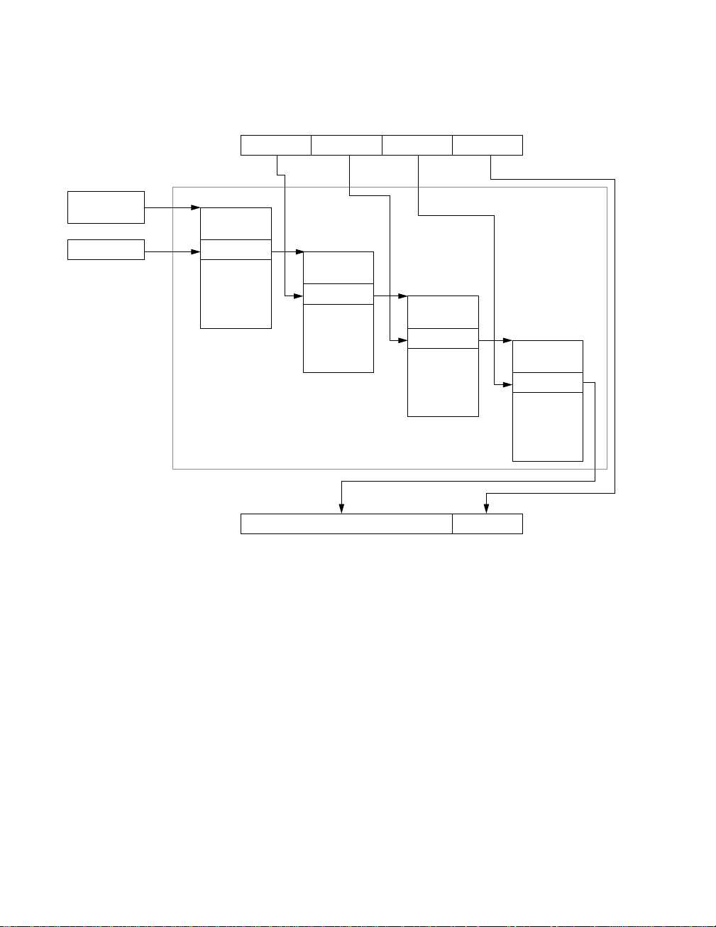
Cache Controller and Memory Management Unit
31 24 23 18 17 12 11 0
Virtual Address Index 1 Index 2 Index 3 Page Offset
Context Table
Pointer
Register
Context Register
Context Table
Level 1 Page
Root Pointer
35 12 11 0
Physical Page NumberPhysical Address
Figure 2-5 A Three Level Table Walk In Memory
The Context Table Pointer register provides a pointer to the context table,
and the context register provides an index to the Root Pointer, which in turn
points to a level 1 page table. Index 1 from the virtual address selects an
entry within Level 1 pointing to a level 2 page table, where Index 2 selects
a pointer to a level 3 table. Index 3 then selects one of the entries in the level
3 table which should point to a 4Kbyte memory page. When a page table
pointer (PTP) is encountered within the tables, the search continues to the
next lower level. If a page table entry (PTE) is found, the search is
terminated and the entry is stored in the TLB. If no PTE is found at all, a
synchronous fault exception is signalled to the IU. The PTE provides a
pointer to a physical page while, in the case of a three level table walk, the
lower 12 bits of the virtual address provides an offset.
Table
PTP
Level 2 Page
Table
PTP
Page Offset
Level 3 Page
Table
PTE
2-12 The SPARC CPU
Page 41
Cache Controller and Memory Management Unit
The level at which a table walk terminates (that is, a PTE is found) is related
to the size of addressing region associated with the entry. A table walk
which finds a PTE in the context table corresponds to a region of 4Gbytes.
A PTE corresponds to: a 16Mbyte region in level 1; a 256Kbyte region in
level 2; or a 4Kbyte region in level 3. The virtual address bits not used to
index table entries are used to supply the offset address within the page.
A table walk which uses three page table levels is shown in the illustration
in Figure 2-5. In this example A(31:12) from the virtual address are used to
index the page tables, and A(11:0) supply an offset address into the selected
memory page.
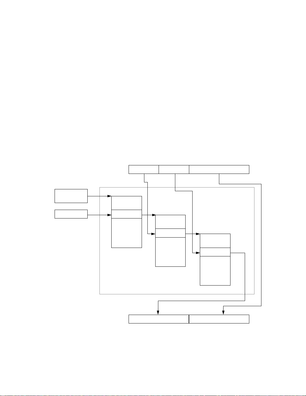
Figure 2-6 shows a table walk which terminates at level 2. In this case
A(31:18) are used as index bits, and A(17:0) provide an offset address into
the selected 256 Kbyte page.
31 24 23 18 17 0
Virtual Address Index 1 Index 2 Offset
Context Table
Register
Pointer
Context Register
Context Table
Root Pointer
35 18 17 0
Physical Page NumberPhysical Address
Figure 2-6 A Two Level TableWalk In Memory
Level 1 Page
Table
PTP
Level 2 Page
Table
PTE
Byte Offset
The SPARC CPU 2-13
Page 42

2.5 Memory Interface
The SPARC provides a 64-bit memory interface which supports up to
128Mbytes of system memory. The memory is composed of four banks of
up to 32Mbytes each. Different density devices are supported, allowing the
SPARCbook 3 to be fitted with a range of memory size options.
The SPARC’s memory interface provides a 64-bit data bus with 2-bit parity
(1 bit parity for each 32 bit word). The memory interface incorporates a
DRAM refresh controller.
The minimum memory access width is 32 bits; 8-bit and 16-bit write
accesses require read-modify-write operation and correct 32-bit boundary
alignment.
2.6 Instruction Cache
The integral instruction cache is a 16Kbyte physically tagged cache. The
instruction cache is organized as 512 lines of 32 bytes each.
2.7 Data Cache
Memory Interface
The data cache is a 8Kbyte direct mapped physically tagged write through
cache with no write allocate. It is organized as 512 lines of 16 bytes each.
Data cache read and write hits take no extra pipe cycles, except for
doubleword operations. There are two store buffers which hold data being
stored from the IU or FPU to memory or other physical devices. The store
buffers are 32-bit registers.
2.8 SBus Controller
The SPARC incorporates an SBus Controller which provides a master and
slave interface used to access I/O devices. It connects the CPU core directly
to the SBus and allows DMA devices to access the main DRAM located on
the SPARC’s memory bus. The SBus controller provides 32-bit data,
SBD(31:00), and 28-bit physical address, SBA(27:00), interface to other
devices in SPARCbook 3. The SBus controller also provides five SBus
Slave Select lines, SBSEL(4:0).
2-14 The SPARC CPU
Page 43

SBus Controller
2.8.1 Programmed I/O
Programmed I/O transactions consist of an SBus slave cycle only, with
address translations being carried out before bus acquisition. The processor
executes loads and stores to transfer data between it and devices on the
SBus (in I/O Space). The SBus Controller performs write posting during
processor writes, allowing processing to continue while the SBus
transaction is completed. During reads, processing is stalled until the data
becomes valid at the end of the SBus transaction.
2.8.2 DVMA
A direct virtual memory access consists of a translation cycle followed by
a slave cycle. During the translation cycle, a master places a virtual address
on the SBus data bus. The SPARC’s MMU provides a translated physical
address on the SBus.
The SPARC CPU 2-15
Page 44

SBus Controller
2-16 The SPARC CPU
Page 45

Memory Map and Interrupts 3
This chapter describes the addressing architecture
and interrupt architecture of SPARCbook 3.
The SLAVIO incorporates an interrupt controller
and is used to coordinate all on-board interrupts.
These include interrupts from devices on the board
and interrupts from SLAVIO internal source.
33
Page 46

3.1 Address Map
Address Map
The SBus controller contained in the MicroSPARC partitions the
SPARCbook 3’s memory map into a region for the main memory plus five
physical address regions of 256Mbytes each for the SBus. The resulting
memory map of the SPARCbook is shown in Table 3-1.
Address Range
(Hexadecimal)
70000000 7FFFFFFF SBus Slot 4 MACIO/SLAVIO 256
60000000 6FFFFFFF SBus Slot 3 Not allocated 256
50000000 5FFFFFFF SBus Slot 2 ISDN Controller 256
40000000 4FFFFFFF SBus Slot 1 TS102 PCMCIA Controller 256
30000000 3FFFFFFF SBus Slot 0 P9100 Graphics Controller 256
20000000 2FFFFFFF Unmapped - 256
10000000 1FFFFFFF I/O MMU Control Space - 256
08000000 0FFFFFFF Unmapped - 128
06000000 07FFFFFF DRAM Bank 3 - 32
04000000 05FFFFFF DRAM bank 2 - 32
02000000 03FFFFFF DRAM Bank 1 - 32
00000000 01FFFFFF DRAM Bank 0 - 32
Region SBus Rsource
Table 3-1 Main Memory Map
3.1.1 MACIO and SLAVIO Space (SBus Slot 4)
SBus slot 4 is sub-divided to provide access to the MACIO and SLAVIO.
These two devices are designed to operate as a pair, and each device has a
direct SBus connection.
Size
(Mbytes)
The MACIO device incorporates DMA controllers, an Ethernet controller,
a bi-directional parallel interface, and a SCSI bus controller. The DMA
controllers provide support for the Ethernet, parallel and SCSI interfaces,
including FIFO support, and allow burst transfers to be performed on the
SBus.
Connected to the SLAVIO but isolated from the SBus are the Boot ROM,
the O/S ROMs, the RTC and NVRAM, modem and Audio devices.
3-2 Memory Map and Interrupts
Page 47

Address Map
The map for SBus Slot 4 is as shwon in Table 3-2.
Address Range
(Hexadecimal)
78000000 7FFFFFFF MACIO 128
70000000 77FFFFFF SLAVIO 128
Table 3-2 SBus Slot 4 Memory Map
Resource
Size
(Mbytes)
The MACIO provides processor accessible control ports for DMA related
operations, for parallel port operations, for SCSI operations and for
network interface control.
Base Address
(Hexadecimal)
7C800000 Parallel Port Registers
78C00000 Network Controller Registers
78800000 SCSI Registers
78400000 DMA Control and Test Registers
78000000 Internal ID Register
Table 3-3 MACIO Port Locations
Port
The function and access sizes of these locations are discussed in the
relevant chapter for each interface.
The SLAVIO contains a number of internal devices. These are a floppy
controller (not used in SPARCbook 3), two serial controllers (SCCs),
counter/timers and an interrupt controller. The SLAVIO also supports
access to external devices via the EBus.
The internal interface devices each present an independent interface to the
host. Details of these control interfaces are provided in the relevant chapter
for each interface.
Within their assigned spaces in the SLAVIO’s address space, the
RTC/NVRAM and Boot PROM are mapped repeatedly. In the case of the
RTC/NVRAM this means that there are 256 images.
The SLAVIO memory map is shown in Table 3-4.
Memory Map and Interrupts 3-3
Page 48

Address Map
Offset Range
(Hexadecimal)
1F00000 1FFFFFF SLAVIO System Controller and Status Register Word
1E00000 1EFFFFF SLAVIO Interrupt Controller Word
1D00000 1DFFFFF SLAVIO Counter/Timers Word, Doubleword
1C00000 1CFFFFF SLAVIO Reserved
1B00000 1BFFFFF SLAVIO Modem Register Byte
1A00000 1AFFFFF SLAVIO Diagnostic Message Register Byte
1900000 19FFFFF SLAVIO Auxiliary I/O Registers Byte
1800000 18FFFFF SLAVIO Configuration Registers Byte
1500000 17FFFFF SLAVIO Reserved
1400000 14FFFFF SLAVIO Floppy Controller Byte
1380000 13FFFFF Paged FLASH O/S ROM Byte
1304000 137FFFF Echoes of Audio and Auxiliary Port Byte
1302000 1303FFF Auxiliary Control/Status Port Byte
1300000 1301FFF Audio Device Byte
1204000 12FFFFF Echoes of RTC/RAM and Diagnostic LEDS Byte, Halfword, Word
1202000 1203FFF RTC/RAM and Diagnostic LEDs Byte, Halfword, Word
1200000 1201FFF RTC/RAM Byte, Halfword, Word
1000000 11FFFFF SLAVIO Keyboard/Mouse/Serial Byte
0800000 0FFFFFF Echo of Boot and O/S ROMs Read Only, Byte, Halfword, Word
0700000 07FFFFF O/S ROM 4 Read Only, Byte, Halfw ord, Word
0600000 06FFFFF O/S ROM 3 Read Only, Byte, Halfw ord, Word
0500000 05FFFFF O/S ROM 3 Read Only, Byte, Halfw ord, Word
0400000 04FFFFF O/S ROM 1 Read Only, Byte, Halfw ord, Word
0100000 03FFFFF Echoes of Boot ROM Read Only, Byte, Halfw ord, Word
0000000 00FFFFF Boot ROM Read Only, Byte, Halfword, Word
Resource Accessibility
3-4 Memory Map and Interrupts
Table 3-4 SLAVIO Memory Map
Page 49

Interrupts
3.1.2 DRAM
The DRAM address multiplexers support SIMM units with up to 11 x 11 or
(12 x 10) Row/Column multiplex (1Mbit, 4Mbit, and most 16Mbit
devices). Each SIMM module can contain one or two banks of memory.
SIMM sizes up to 64Mbytes are supported, with a maximum of 32Mbytes
per bank.
The memory maps for the different configurations are based on the
principle that the individual bank selects (RAS signals) are derived from
the address decodes for fixed 32Mbyte memory segments.
Table 3-8 summarizes the possible memory implementations when using
identical SIMM pairs.
SIMMs
System
Capacity
16Mbytes 2 2M by 33 Two banks of 4Mbit At 0 & 32Mbytes for 8Mbytes each
32Mbytes 2 4M by 33 One bank of 16Mbit At 0 for 32Mbytes
64Mbytes 2 8M by 33 Two banks of 16Mbit At 0 for 64Mbytes
128 Mbytes 2 16M by 33
Qty Organization*
Architecture of
Each
Address Map
(Where memory appears)
3.2 Interrupts
Table 3-5 DRAM Mapping
*Figures in the Organization column can be either by 33 or by 36.
Interrupts from devices within SPARCbook 3 are signaled to the
microSPARC as a 4-bit priority encoded value on S_IRL(3:0). Control of
interrupts and prioritization is carried out by the SLAVIO. The
microSPARC provides a structure of traps which supports fifteen external
interrupts.
The SLAVIO contains interrupt control and mask registers which are used
to enable and clear hardware interrupts from devices within the
SPARCbook 3 system as well as interrupts from devices internal to the
SLAVIO and MACIO. The SLAVIO also provides software generated
interrupts on each of fifteen levels.
Memory Map and Interrupts 3-5
Page 50

The interrupts in SPARCbook 3 can be considered as belonging to three
categories: SLAVIO interrupts, MACIO interrupts, and SBus interrupts.
The SLAVIO interrupts include those from the internal serial ports and
timers and the software interrupts. The MACIO interrupts include the
Ethernet, SCSI and parallel port interrupts.
Table 3-6 provides a summary of the interrupt request sources within
SPARCbook 3.
Source
Level
SLAVIO MACIO SBus
0 No Interrupts Pending
1 SOFTINT 1 - 2 SOFTINT 2 - IRQ1
3 SOFTINT 3 Parallel Port IRQ2
4 SOFTINT 4 SCSI 5 SOFTINT 5 - IRQ3
6 SOFTINT 6 Ethernet 7 SOFTINT 7 - IRQ4
8 SOFTINT 8 - 9 SOFTINT 9 - IRQ5
10 SOFTINT 10, Sys Counter/Timer - 11 SOFTINT 11, Floppy - IRQ6
12 SOFTINT 12, Serial/KBD/MSE - 13 SOFTINT 13, Audio - IRQ7
14 SOFTINT 14, Proc Coun-
ter/Timer
15 SOFTINT 15 Async. Hardware Errors.
- -
-
User Power-Down Request
Interrupts
3-6 Memory Map and Interrupts
Table 3-6 SPARCbook Interrupts
Page 51

Interrupts
3.2.1 Interrupt Control
The SLAVIO provides a number of interrupts status and control locations.
The processor group provides interrupt pending information and control
over software interrupts. The system group provides enable and clearing
control over the individual hardware interrupt requests.
Processor Group
Address
(Hexadecimal
Device or Register Access
)
71E00000 Processor Interrupt Pending R
71E00004 Processor Clear Pending W
71E00008 Processor Set Software Interrupt W
71E10000 System Pending Interrupt Register R
71E10004 System Interrupt Target Mask Register R
71E10008 System Interrupt Target Mask Clear W
71E1000C System Interrupt Target Mask Set W
Table 3-7 Interrupt Control Registers
SOFTINT(15:1) HARDINT(15:1)
31 17 16 15 0001
Processor Interrupt Clear Pseudo-register
SOFTINT(15:1) CLEAR
31
Processor Set Soft Interrupt Pseudo Register
SOFTINT(15:1) SET
31
Figure 3-1 Processor Interrupt Registers
Processor Interrupt Pending Register
IC
171716
15
16
00
00
Memory Map and Interrupts 3-7
Page 52

System Group
Interrupts
SOFTINT(15:1)
Software Interrupt
HARDINT(15:1)
Hardware Interrupt
IC Interrupt Level 15 Clear
Writing a ‘1’ to any of the SOFTINT bits or IC bit in the Interrupt Clear
pseudo-register clears the associated interrupt.
The Set Soft Int pseudo-register is used to generate software interrupts.
Setting a bit in this register sets the associated bit in the pending register and
triggers an interrupt request on the appropriate level.
MAME I* M* F V* T SC E S K SBus IRQ(7:1)
31 16 15 14 0030 29 28 27 23 22 21 20 19 18 17 13 07 06
System Interrupt Pending Register
System Target Mask Register (R)
System Target Mask Set Register(W) and
System Target Mask Clear Register (W)
Figure 3-2 System Interrupt Registers
Bit 31 MA – Mask all Interrupts (reserved in the System Interrupt
Bit 30 ME – Module Error
Bit 29 Reserved on SPARCbook
Bit 28 Reserved on SPARCbook
Bits 27:23 Reserved
Bit 22 F – Floppy Interrupt
Bit 21 Reserved
Bit 20 Reserved on SPARCbook
Bit 19 T – Level 10 Counter/Timer
Bit 18 SC – SCSI Interrupt
3-8 Memory Map and Interrupts
Pending Register)
1= disable all interrupts
Page 53

NCR89C105 SLAVIO Configuration Control
Bit 17 Reserved
Bit 16 E – Ethernet Interrupt
Bit 15 Bit S – Serial Port Interrupt (SLAVIO)
Bit 14 K – Keyboard/Mouse Interrupt
Bits 13:07 SBus IRQ (7:1)
Bits 06:00 Reserved
3.3 NCR89C105 SLAVIO Configuration Control
3.3.1 SLAVIO Configuration Register
The NCR89C105 has several software-programmable options which are
controlled by its configuration register. This register is located at
0x70180000.
P D M S
Reserved
7 6 5 4 3 2 1 0
I
Figure 3-3 The SLAVIO Configuration Register
A system reset clears all of the SLAVIO configuration bits to 0.
Field definitions:
Bits 7:5 Reserved - always read 0.
Bit 4 I - Modem Ring Interrupt Enable. When this bit is set to 1,
the modem RI interrupt generation is activated (see also Bit
1, and the description of the modem register). When this bit
is cleared, modem interrupts are not generated, regardless of
the state of the M bit (Bit 1) or the MSI_IRQ_input.
Bit 3 P - Power Fail Detect Enable. When this bit is set to 1, a lo w
on the PFD_input causes a module error (error 15) interrupt.
The interrupt is visible (and clearable) in AuxIO register 2.
When this bit is clear, the PFD_input is ignored.
Memory Map and Interrupts 3-9
Page 54

NCR89C105 SLAVIO Configuration Control
Bit 2 D - Density Select Source (1 = 82077 density select, 0 =
82077 motor enable #2). - This bit determines which signal
drives the external density select pin (FPY_DENSEL).
Bit 1 M - Modem Ring Select. When this bit is set to 1, a low on
the MSI_IRQ_input causes a level 15 MSI interrupt. When
this bit is cleared, a transition causes a modem ring indicate
interrupt (SBus level 5). Either a low or high transition can
cause an interrupt in this mode, depending on the Edge
Select bit in the modem register . The unused input is held in
its inactive state.
Bit 0 S - SuperSPARC mode (1 = SuperSPARC, 0 =
MicroSPARC-II). This bit determines the function of several
multiplexed input pins (the NCR89C105 unsufficient pins to
support all functions concurrently). The muxed pins are
shown in Table 3-8:
Pin microSPARC Use SuperSPARC Use
ser_rtxc_b ser_rtxc_b_ emc_irq_
iu_error_ iu_error_ video_irq
Table 3-8 microSPARC-II/SuperSPARC Muxed Pins
In microSPARC-II mode, the SuperSPARC interrupts are inactive.
3.3.2 Diagnostic Messages
The Diagnostic Message Register is an 8-bit read/write register provided
for diagnostic use. Accesses to this register change the value that is stored
in it.
Figure 3-4 Diagnostic Message Register
Field definitions:
Bits 7:0 (D) - Diagnostic value. This value is read/writeable, and is
3-10 Memory Map and Interrupts
D
7 6 5 4 3 2 1 0
preserved across resets.
Page 55

NCR89C105 SLAVIO Configuration Control
Note
All bits in the Diagnostic Message Register are unaffected by system resetbut
contains random information after a power-on reset.
3.3.3 Miscellaneous System Functions
The NCR89C105 contains two 8-bit Auxiliary I/O Registers: one dedicated
to controlling system power-down; and one used to support several
hardware functions that do not fit well elsewhere. These registers are
located at physical addresses 0x7190000 (aux1) and 0x719100000 (Aux 2).
LED/Floppy (Aux 1)Register
D
7 6 5 4 3 2 1 0
Figure 3-5 Auxiliary I/O Register 1
A system reset clears all output bits (Bits 3, 2, 1, and 0) to 0. The
FPY_DENSENSE chip pin controls input bit (Bit 5). The unused bits (Bits
4, 6, and 7) are unaffected by writes, and always read 0.
Bits 7:6 Reserved - always read 0.
Bit 5 D - Floppy Density Sense (not used).
Bit 4 Reserved - always read 0.
Bit 3 E - Link Test Enable. This bit is directly reflected in the
LINK_TEST_EN pin. It controls the AT&T 7213 LTE pin.
Bit 2 M - Monitor/Mouse Mux. This bit is directly reflected on the
MON_MSE_MUX pin.
Bit 1 T - T erminal Count (1 = TC). Writing a 1 to this bit sends a 4
SBus clock wide TC pulse to the 82077 floppy controller.
This bit is self-clearing; it always reads 0. Writing a 0 has no
effect.
Bit 0 L (1 = on, 0 = off). - This bit controls the system LED on the
front panel.
E M T L
Memory Map and Interrupts 3-11
Page 56

NCR89C105 SLAVIO Configuration Control
Power Down Control (Aux 2) Register
D
7 6 5 4 3 2 1 0
C F
Figure 3-6 Auxiliary I/O Register 2
All Bits are cleared to 0 on system reset.
Bits 7:6 Reserved. These bits should be masked, and their values
should be discarded by the software. These bits can be read
and written to, but the values have no meaning or effect.
Bit 5 D - Power Failure Detect (1 = power fail). When the power
fail detect signal from the power supply is low, this bit is set,
and a module error interrupt is generated (this is a level 15
interrupt). Writing a 1 to Bit 1 of this register, or disabling
PFD in the Config register clears this bit. This bit is also set
if BUFP or PWROK are set to 0.
PFD* input is ignored if Bit 5 is disabled in the Config
register.
Bits 4:2 Reserved. These bits should be masked, and their values
should be discarded by the software. These bits can be read
and written to, but the values have no meaning or effect.
Bit 1 C - Clear Power Fail Detect (1 = clear). This bit clears the
interrupt generated by PFD_ and Bit 5 of this register.
Writing 0 has no effect.
Bit 0 F - Power off (1 = off). This bit is reflected in the power
3-12 Memory Map and Interrupts
output pin. When this bit is set to 1, the power supply turns
off.
Page 57

NCR89C105 SLAVIO Configuration Control
Modem Register The NCR89C105 can directly support the RI (Ring Indicate) bit output of
a modem, when it is configured for modem use. This mode uses the
MSI_IRQ_ input pin for sensing modem RI. When the Modem mode and
the Modem interrupt are enabled in the Configuration Register, the
NCR89C105 generates an SBus level 5 interrupt on RI transitions.
E IR
7 6 5 4 3 2 1 0
Figure 3-7 Modem Register
A system reset clears Bits 1 and 0 to 0. The input bit 2 is controlled by the
MSI_IRQ_ chip pin. Bits 7:3 are unaffected by resets or writes and always
read as 0.
Bits 7:3 Reserved - always read 0.
Bit 2 R - RI pin. This pin directly reflects the state of the
MSI_IRQ_ pin (which is used for modem RI when in
Modem mode). If this pin is low, then this bit is 0.
Bit 1 E - Edge Select. This bit selects which RI edge causes an
interrupt. When this bit is cleared to 0, a 1 to 0 transition on
the MSI_IRQ_ pin causes an interrupt. Toggling this bit
after the first edge of an RI pulse is received, allows
interrupts to be obtained on both edges of RI.
Bit 0 I - Modem RI Interrupt. This bit is set to 1 if a modem RI
interrupt is pending. When this happens, an SBus level 5
interrupt is set. Writing a 0 to this bit clears the interrupt.
Memory Map and Interrupts 3-13
Page 58

NCR89C105 SLAVIO Configuration Control
3-14 Memory Map and Interrupts
Page 59

Serial Interface 4
44
The SPARCbook is equipped with two Z85C30
Serial Communications Controllers (SCC), both of
which are contained within the SLAVIO. Although
packaged in the SLAVIO, the two SCCs appear to
software to be fully independent devices.
One is a fully functional SCC and one has reduced
functionality being intended for keyboard and
mouse interfacing.
The architecture of the SPARCbook serial interface
is shown in Figure 4-1.
Cha A
Cha B
SBus
Full Function
SCC
Keyboard
Port
Mouse
Port
Sub-set SCC
Figure 4-1 Serial Interface Architecture
RS232
Transceiver
RS232
Transceiver
Serial
Channel A
Serial
Channel B
Keyboard/
Mouse Port
Page 60

4.1 Serial Channel Assignment
There are four serial channels on the SPARCbook, which are controlled by
SCCs within the SLAVIO. Each channel provides a control interface. Serial
Channels A and B are controlled via the Full-Function SCC; the keyboard
and mouse port (which is Sun compatible) is controlled via the sub-set
SCC.
Connector pinout details are provided in Appendix B, “Connector
Information”.
4.1.1 Serial Interface Control
Table 4-1 summarizes the addresses of the four serial channels present on
the SPARCbook.
Serial Channel Assignment
Address
(Hexadecimal)
Device Channel
SLAVIO Full-Function SCC
71100000 TTYB Control
71100002 TTYB Transmit and Receive Buffers
71100004 TTY A Control
71100006 TTY A Transmit and Receive Buffers
SLAVIO Sub-Set SCC
71000000 Mouse Control
71000002 Mouse Data
71000004 Keyboard Control
71000006 Keyboard Data
Table 4-1 Serial Ports Addressing and Assignment
The SCC provides an 8-bit host interface. The SLAVIO internal registers
appear on D(7:0); the data on the remainder of the bus during an SCC
access is undefined.
A detailed programming discussion is beyond the scope of this manual; for
further information, please refer Appendix A, “Further Information”.
Assignment on
SPARCbook
Serial Channel B 8-pin mini-DIN
Serial Channel A 8-pin mini-DIN
Keyboard/Mouse Port 8-pin mini-DIN
Connector
4-2 Serial Interface
Page 61

SCC Registers
4.2 SCC Registers
The SCC internal registers are accessed using a register pointer to perform
selection. First, the register pointer bits in WR0 are programmed to specify
the register to be accessed. Then, a read or a write is performed at the same
address to transfer data into or out of the selected register. When the access
to the selected register has been completed, the register pointer bits are reset
to ‘0’.
Three pointer bits in WR0 allow access to the lower eight registers
locations, but WR0 also contains 3-bit command word (D5:D3) in which
the ‘Point High’ command, 001(bin), is required to gain access to the upper
eight register locations. The receive buffer and transmit buffer, RR8 and
WR8 respectively for each channel can be accessed in a single read or write
operation.
4.2.1 Register functions
The Z82530 SCC contains fifteen write registers (WR0 to WR15) for each
channel. WR8 is the transmit buffer and the remainder are used to configure
the SCC for the required operation. Two registers (WR2 and WR9) are
shared by both channels. Each channel also has nine read registers (RR0 to
RR3, RR8, RR10, RR12, RR13 and RR15). RR8 is the receive buffer and
the remainder provide status information.
Table 4-11 shows the full suite of registers present in the external 85C30
SCC and full-function internal SCC. The sub-set SCC does not present the
full set of registers.
Register Function
RR0 Transmit and Receive Buffer status, external status
RR1 Special receive condition status
RR2A, RR2B Unmodified interrupt vector (Ch A only), Modified interrupt vector (Ch B only)
RR3A, RR3B Interrupt pending bits (Ch A only), Null (Ch B only)
RR8 Receive Buffer
RR10 Miscellaneous status
RR12 Lower byte of baud-rate time constant
RR13 Upper byte of baud-rate time constant
Table 4-2 SCC Register Summary
Serial Interface 4-3
Page 62

Register Function
RR15 External/Status interrupt information
WR0 CRC initialize, mode initialization, Register Pointer
WR1 Transmit and Receive interrupt, data transfer mode definitions
WR2 Interrupt vector (CH A and B)
WR3 Receive Parameters and controls
WR4 Transmit and receive parameters and controls
WR5 Transmit parameters and control
WR6 Synchronization character or SDLC address field
WR7 Synchronization character or SDLC flag
WR8 Transmit Buffer
WR9 Master Interrupt control and reset (CH A and B)
WR10 Miscellaneous controls
WR11 Clock mode control
WR12 Lower byte of baud-rate time constant
WR13 Upper byte of baud-rate time constant
WR14 Miscellaneous control
WR15 External/Status interrupt control
SCC Registers
Table 4-2 SCC Register Summary (Continued)
WR0 Bits 7:6 Resets
00 = Null
01 = Reset Rx CRC checker
10 = Reset Tx CRC generator
11 = Reset Tx underrun/OEM latch
Bits 5:3 Commands
000 = Null
001 = Point High (reg 8-15 select)
010 = Reset external/status interrupts
011 = Send abort (SDLC mode)
100 = Enable int on next Rx character
101 = Reset Tx interrupt pending
110 = Error reset
111 = Reset highest IUS
Bits 2:0 Register 0-7 or 8-15 select
4-4 Serial Interface
Page 63

SCC Registers
WR1 Bit 7 Wait/DMA request enable
WR3 – Receive Parameters and Control
Bit 6 W
Bit 5 Wait/DMA request on Rx/Tx
Bit 4:3 Receive interrupt control
Bit 2 Parity as special condition enable
Bit 1 Tx interrupt enable
Bit 0 External interrupt enable
Bits 7:6 Bits/character
Bit 5 Auto enables
Bit 4 Enter hunt mode
Bit 3 Receiver CRC enable
Bit 2 Address search mode
ait/DMA request
00 = Interrupt disable
01 = Interrupt on first char or special condition
10 = Interrupt on all chars or special condition
11 = Interrupt on special condition only
00 = 5 bits
01 = 7 bits
10 = 6 bits
11 = 8 bits
WR4 – Transmit and Receive Parameters and Control
Bit 1 Sync character load inhibit
bit 0 Receiver enable
Bits 7:6 Clock mode
00 = x1
01 = x16
10 = x32
11 = x64
Bits 5:4 Sync Mode
00 = 8-bit sync character
01 = 16-bit sync character
10 = SDLC mode
11 = External sync mode
Bits 3:2 Stop mode
Serial Interface 4-5
Page 64

00 = Sync modes enabled
01 = 1 stop bit/character
10 = 1.5 stop bits/character
11 = 2 stop bits/character
SCC Registers
WR5 – Transmit Parameters and Control
WR9 – Interrupt Control and Reset
Bit 1 Parity Even/Od
d
Bit 0 Parity enable
Bit 7 DTR
Bits 6:5 Bits/character
00 = 5 bits
01 = 7 bits
10 = 6 bits
11 = 8 bits
Bit 4 Send Break
Bit 3 Transmitter enable
Bit 2 SDLC/CRC-16
Bit 1 RTS
Bit 0 Transmitter CRC enable
Bits 7:6 Reset control
00 = no reset
01 = Reset Channel B
10 = Reset Channel A
11 = Force hardware reset
Bit 5 Reserved (Write 0)
WR10 – Miscellaneous Controls
4-6 Serial Interface
Bit 4 Status High/Low
Bit 3 Master interrupt enable
Bit 2 Disable lower chain
Bit 1 No vector or interrupt acknowledge
Bit 0 Vector include status
Bit 7 CRC Preset
Bits 6:5 Mode
Page 65

SCC Registers
00 = NRZ
01 = NRZI
10 = FM1
11 = FM0
Bit 4 Active on poll
WR11 – Clock Mode Control
WR14 – Miscellaneous Control
Bit 3 Mark/Fla
Bit 2 Abort/Flag on idle
Bit 1 Loop mode
Bit 0 6-bit/8-bit Sync
Bit 7 RTXCb XTAL/No XTAL
Bits 6:5 Receive clock source
Bits 4:3 Transmit clock source
Bit 2 TRXC Enable (Write 0)
Bits 1:0 Not used
Bit 7:5 Clock Mode
g on idle
00 - 01 = Reserved
10 = Baud rate generator
11 = Reserved
00 - 01 = Reserved
10 = Baud rate generator
11 = Reserved
000 = Null
001 = Enter search mode
010 = Reset missing clock
011 = Disable DPLL
100 = Clock source is BR generator
101 = Clock source is RTXCb
110 = FM mode
111 = NZRI Mode
Bit 4 Local loopback
Bit 3 Auto echo
Bit 2 DTRb/Request function
Bit 1 BR generator source
Bit 0 BR generator enable
Serial Interface 4-7
Page 66

SCC Registers
WR15 – External/Status Interrupt Control
Bit 7 Break/Abort Interrupt enable
Bit 6 Tx Underrun/EOM Interrupt enable
Bit 5 CTS enable
Bit 4 Sync/Hunt enable
Bit 3 DCD interrupt enable
Bit 2 Reserved (write 0)
Bit 1 Zero count interrupt enable
Bit 0 Reserved (write 0)
RR0 – Status Bit 7 Break/Abort
Bit 6 Transmit underrun/EOM
Bit 5 CTS
Bit 4 Sync/Hunt
Bit 3 DCD
Bit 2 Transmit Buffer empty
Bit 1 Zero count interrupt enable
Bit 0 Receive character available
RR1 – Special Receive Condition
Bit 7 End of frame
Bit 6 CRC/Framing error
Bit 5 Receive overrun error
Bit 4 Parity error
Bit 3 Residue Code 0
Bit 2 Residue Code 1
Bit 1 Residue Code 2
Bit 0 All sent
RR3 – Interrupt Pending RR3 returns zero when read via channel B
Bits 7:6 00
Bit 5 Channel A Rx
Bit 4 Channel A Tx
4-8 Serial Interface
Page 67

SCC Registers
Bit 3 Channel A EXT/STAT
Bit 2 Channel B Rx
Bit 1 Channel B Tx
Bit 0 Channel B EXT/STAT
RR10 – Miscellaneous Status
RR15 – External/Status Interrupt Status
Bit 7 One clock missing
Bit 6 Two clocks missing
Bit 4 Loop sending
Bit 1 On loop
Other bits 0
Bit 7 Break/Abort interrupt enable
Bit 6 Tx Underrun/EOM interrupt enable
Bit 5 CTS interrupt enable
Bit 4 Sync/Hunt interrupt enable
Bit 3 DCD interrupt enable
Bit 1 Zero count interrupt enable
Other bits 0
Serial Interface 4-9
Page 68

4.3 Baud Rate Clocks
A 19.66 MHz clock signal generated by the MACIO is used to derive a
baud rate clock for all of the SCCs. This is divided by four before being fed
to the SCCs at 4.915 MHz. The baud rate can be changed by loading
different time constants (which can be different for each channel) into the
time constant register. The clocking modes 1, 2, 16, 32 and 64 are
supported.
The SCCs can be operated at baud rates of between 75 and 19200. This is
controlled by the clocking mode and the contents of the time constant
register. The value of the time constant can be determined using the
following equation:
Baud Rate Clocks
4.4 Handshakes
Tc
-------------------------------------------------------------------- 2–=
2 Mode( )× Buadrate( )×
Clock
For example, to set a baud rate of 9600 using the x16 clocking mode on the
SPARCbook, the following would be used:
Tc
4.915
------------------------------
2 16× 9600×
6
×
10
2–=
This gives a time constant of approximately 14 (0xD).
With the exception of the mouse and keyboard port, the serial channels all
support handshaking. The handshake signals are controlled or monitored
via the write registers and read registers of the associated SCC channel.
4-10 Serial Interface
Page 69
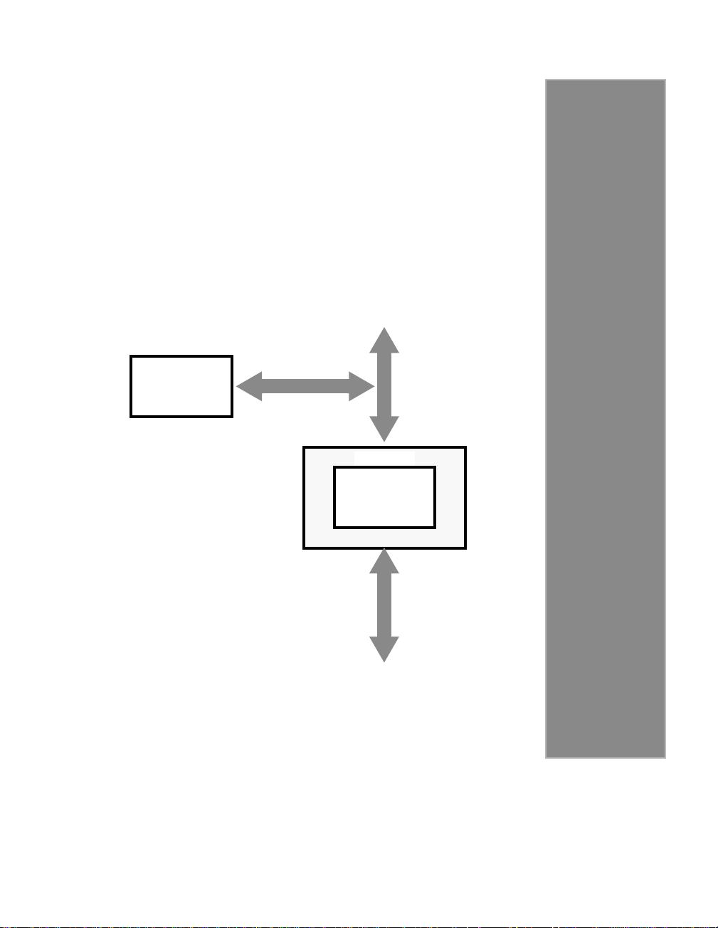
SCSI Controller 5
The MACIO incorporates an enhanced NCR53C90
Fast SCSI Controller (FSC), which supports
SCSI-2 operations at up to 10 Mbytes/sec running
synchronously. SCSI transfers are supported by the
MACIO’s integral DMA controller.
SCSI Connector
(on I/O Panel)
55
Removable
SCSI
Drive
Figure 5-1 SCSI Architecture
SCSI
Bus
MACIO
NCR 53C90
SCSI
Controller
SBus
Page 70

5.1 Connecting SCSI Devices
The SPARCbook provides a 30-pin high density (Hosiden style) connector,
to which you can connect the supplied SCSI adapter cable. This cable
provides a 50-way high density SCSI-2 connector that can be used to make
connection to SCSI devices.
5.2 NCR53C9X SCSI Controller
The FSC is a high performance superset of the NCR53C90 ASC and
provides fast SCSI operation with additional commands and an additional
configuration register. Speed of operation is enhanced by the MACIO’s
integral DMA controller.
The FSC provides full support of ANSI X3.131 SCSI and SCSI-2 standard.
5.2.1 53C9X register set
The SCSI controller internal registers appear from base address
0x78800000. Table 5-1 shows the address offset of the SCSI internal
registers.
Connecting SCSI Devices
5-2 SCSI Controller
Address Register Access
0x78800000 Transfer Count Low Register R/W
0x78800004
0x78800008
0x7880000C
0x78800010
0x78800014
0x78800018
0x7880001C
0x78800020
Transfer Count Mid Register R/W
FIFO Data Port Register R/W
Command Port Register R/W
Status Port Register R
Select / Reconnect Bus ID register W
Interrupt Status Register R
Select / Reconnect Timeout Register W
Sequence Step Register R
Sync Period Register W
FIFO Flags Register R
Sync Offset register W
Configuration 1 Register R/W
Table 5-1 FSC Register Set
Page 71

NCR53C9X SCSI Controller
Address Register Access
0x788000
24
0x78800028
0x7880002C
0x78800030
0x78800038
Clock Conversion Register W
Test Mode W
Configuration 2 Register R/W
Configuration 3 Register R/W
Transfer Counter High Register R/W
Table 5-1 FSC Register Set (Continued)
There follows a brief description of the FSC registers. A detailed
programming description of the device is beyond the scope of this manual
and the user should refer to the bibliography at the rear of this document.
Command Register The Command Register is a double-buffered register that allows two
commands to be written to the FSC consecutively. Bit 7 controls the
enabling of DMA operations and bits 6:0 provide a command code. Within
the command code, bits 6:4 control the operating mode, of which only one
can be selected at any time.
Bit 7 Enable DMA
0 = DMA Mode Disabled
1 = DMA Mode Enabled
Bit 6:4 Select Mode, see Table 5-2
An interrupt is generated if an invalid mode for the FSC is specified by bits
6:4, or if the command is not supported. Table 5-2 shows the commands
selectable using bits 6:0.
SCSI Controller 5-3
Page 72

NCR53C9X SCSI Controller
Command Register Value
Command Interrupt
7 6 5 4 3 2 1 0
Immediate Commands
X 0 0 0 0 0 0 0 No operation NO
X 0 0 0 0 0 0 1 Flush FIFO NO
X 0 0 0 0 0 1 0 Reset 53C90A device NO
X 0 0 0 0 0 1 1 Reset SCSI bus NO
Disconnect Commands
X 1 0 0 0 0 0 0 Reselect Sequence YES
X 1 0 0 0 0 0 1 Select without ATN sequence YES
X 1 0 0 0 0 1 0 Select with ATN sequence YES
X 1 0 0 0 0 1 1 Select with ATN and stop sequence YES
X 1 0 0 0 1 0 0 Enable Selection / Reselection NO
X 1 0 0 0 1 0 1 Disable Selection / Reselection YES
X 1 0 0 0 1 1 0 Select with ATN3 YES
X 1 0 0 0 1 1 1 Reselect Sequence YES
Target Mode Commands
X 0 1 0 0 0 0 0 Send message YES
X 0 1 0 0 0 0 1 Send status YES
X 0 1 0 0 0 1 0 Send data YES
X 0 1 0 0 0 1 1 Disconnect sequence YES
X 0 1 0 0 1 0 0 Terminate sequence YES
X 0 1 0 0 1 0 1 Target command complete sequence YES
X 0 1 0 0 1 1 1 Disconnect NO
X 0 1 0 1 0 0 0 Receive message sequence YES
X 0 1 0 1 0 0 1 Receive command sequence YES
X 0 1 0 1 0 1 0 Receive data YES
X 0 1 0 1 0 1 1 Receive command sequence YES
X 0 1 0 1 1 0 0 Target Abort DMA NO
Initiator Mode Commands
X 0 0 1 0 0 0 0 Transfer information YES
X 0 0 1 0 0 0 1 Initiator command complete sequence YES
X 0 0 1 0 0 1 0 Accept message YES
X 0 0 1 1 0 0 0 Transfer pad YES
X 0 0 1 1 0 1 0 Set ATN NO
X 0 0 1 1 0 1 1 Reset ATN NO
Table 5-2 FSC Commands
5-4 SCSI Controller
Page 73

NCR53C9X SCSI Controller
Status Register The Status register contains the device and interrupt status flags. The Status
register should always be read prior to reading the Interrupt Status register
which will cause bits to clear. The Status register contains Error, Transfer
count and SCSI phase information.
Bit 7 Interrupt
0 = No interrupt pending
1 = Interrupt pending
Bit 6 Gross Error
This bit is set if the top of the FIFO is overwritten; if the top
of the command register is overwritten; if the direction of
DMA and SCSI transfer are in opposition; or if there is an
unexpected phase change in initiator role during a
synchronous data phase.
Bit 5 Parity Error
Bit 4 Terminal Count
Bit 3 Valid Group Code
Bits 2:0 SCSI Phase
000 = Data Out
001 = Data In
010 = Command
011 = Status
100 = Reserved
101 = Reserved
110 = Message Out
111 = Message In
Interrupt Status Register
This register can be used in conjunction with the Status and Sequence Step
register to determine the cause of an interrupt. It includes bits to indicate
SCSI bus reset, disconnect, bus service request, function complete and
selected states.
Bit 7 SCSI Bus
Bit 6 Illegal Command
Bit 5 Disconnect
Bit 4 Bus Service
Bit 3 Function Complete
Bit 2 Reselected
SCSI Controller 5-5
Page 74

Bit 1 Selected with ATN
Bit 0 Selected
NCR53C9X SCSI Controller
Configuration
Registers
The CON1, CON2 and CON3 registers allow various operating modes to
be set up. CON1 is used to control the slow cable mode, parity enable and
test, and the 3-bit SCSI host ID. CON2 provides control of the Tagged
queuing, group 2 command and parity control facilities provided by the
53C90A.
Transfer Count Registers
These combine into a 24-bit counter used by a DMA command, and by the
Command Sequencer to count the decoded length of a received SCSI
command.
FIFO / Flags Register The FIFO is a 16 byte deep buffer between the SCSI bus and the system
memory accessible to the host via the FIFO Register.
The FIFO Flags register is a read only register which indicates the number
of bytes remaining in the FIFO.
Select / Reconnect Register
Clock Conversion Factor Register
This is a 3-bit wide write only register used to specify the destination SCSI
bus ID for a select or reselect command.
This register specifies the clock conversion factor allowing the FSC to be
clocked at different speeds. On the SPARCbook 3, the FSC is clocked at 40
MHz and this register should be loaded with the value 0x00.
Select / Reconnect
This register specifies the time period to wait for a select / reselect response.
Timeout Register
Synchronous T ransfer
Period Register
Sequence Step Register
5-6 SCSI Controller
The Transfer Period register is a 5-bit write-only register that specifies the
minimum time between leading edges of successive REQ or ACK pulses.
The default time is 5 clock cycles, the maximum is 35 cycles.
This provides an incrementing 3-bit sequence count to indicate which steps
of a command sequence have been executed prior to an error or interrupt
condition.
Page 75

DMA Support
5.3 DMA Support
5.3.1 DMA Transfers
5.3.2 DMA Registers
The SCSI controller is provided with DMA support by one channel of the
MACIO integral DMA controller. Between the FSC and Sbus the MACIO
provides a 64-byte deep FIFO (D-FIFO) which is bypassed by CPU
accesses to the FSC’s registers.
A transfer from SCSI to memory is carried out in two phases. First from the
SCSI controller to the DMA controller, and then from the DMA controller
to memory. Similarly, transfers from memory to SCSI are composed of a
transfer into the D-FIFO, and then a transfer between the D-FIFO and SCSI
controller.
Data from the SCSI is written into the D-FIFO until the largest possible
Sbus burst write, as specified in the DMA Controller’s Control and Status
register, to memory can be carried out.
The DMA controller provides four 32-bit registers used to control DMA
operations with the FSC.
5.3.3 SCSI Interrupts
Address Register Size Access
0x78400000 Control and Status Register 32 R/W
0x78400004 Address Register 32 R/W
0x78400008 Byte Count Register 24 R/W
0x7840000C Test Control and Status Register 32 R/W
Table 5-3 SCSI Related DMA Registers
The SCSI controller signals interrupts to the CPU via the SLAVIO
multifunction peripheral on level 4. The interrupt service routine can
establish the cause of the interrupt by examining the contents of first the
status register, and then the interrupt status register.
SCSI Controller 5-7
Page 76

DMA Support
5-8 SCSI Controller
Page 77

Ethernet Interface 6
The Ethernet interface on the SPARCbook is
provided by an NCR92C990 integrated into the
MACIO. This provides AUI connections via a
15-pin D-shell connector. The MACIO enhances
Ethernet operations by providing DMA support.
AUI
AT&T
T7213
Interface Adapter
MACIO
NCR 92C990
LAN Controller
66
Sbus
Figure 6-1 Network Interface Architecture
Page 78

6.1 NCR92C990 Overview
The NCR92C990 is a LAN controller which supports the parameters for an
IEEE 802.3 network interface.
6.1.1 Bus Interface
The LAN controller operates as a bus master or a bus slave device.
As a slave, it provides a 16-bit control interface on the SBus with two
register locations. The CPU accesses the registers during system
initialization, and in response to interrupts. Additional registers in the
MACIO’s DMA controller provide enhanced support for programming
DMA operations.
As a master, it operates independently using DMA operations to transfer
data between the network and data structures in memory. The LAN
controller incorporates two independent 48-byte FIFOs; one for transmit
operations, and one for receive operations.
6.1.2 LAN Interface
The NCR92C990 supports error reporting for diagnostics, addressing,
collision, jabbering, framing, underflow and overflow. It allows internal
and external loopback modes to be configured via the control registers.
NCR92C990 Overview
Physical, logical and promiscuous addressing modes are supported.
Packets can be received containing the full 48-bit destination address for
matching against a physical address programmed during initialization. The
LAN controller will also allow the programming of 64 logical addresses for
matching with an incoming packet’s address header. In the promiscuous
mode, all incoming error free packets are accepted and stored in memory.
6.1.3 Descriptor Management
Buffer management for the LAN controller is handled by a recurrent list of
assignments in memory called descriptor rings. There are separate
descriptor rings for transmit and receive operations. The decriptor rings are
searched to determine the location of the next empty buffer. After a buffer
is filled, the OWN bit in the corresponding descriptor is set. When the
controller detects that the OWN bit is set in a descriptor, it uses the ring
buffer pointer in that descriptor to locate the next data buffer.
6-2 Ethernet Interface
Page 79

LAN Controller Registers
6.2 LAN Controller Registers
Access to the LAN controller’s internal registers is gained via two 16-bit
locations, the Register Data Port (RDP) and Register Address Port (RAP).
The RAP is loaded with an index to the required register, and then the
register data can be read from or written to the RDP.
Address Register Size Access
0x78C00000 Register Data Port (RDP) 16-bit R/W
0x78C00002 Register Address Port (RAP) 16-bit R/W
Table 6-1 LAN Controller Register Locations
6.2.1 Register Indexing
The lower 2 bits in the Register Address Port are used to index the internal
Control and Status Registers. The remaining bits, D(15:2) are reserved. The
encoding of D(1:0) is shown in Table 6-2.
Bit 1 Bit 0 Register
0 0 Control and Status Register 0
0 1 Control and Status Register 1
1 0 Control and Status Register 2
1 1 Control and Status Register 3
6.2.2 Control and Status Register 0
This register contains control, status, error and interrupt information.
15
ERR BAB CE MISS ME RINT TINT IFIN IEN
Figure 6-2 Control and Status Register 0
Table 6-2 Register Indexing
0
RON TON TD STP STR INIT
Ethernet Interface 6-3
Page 80

LAN Controller Registers
ERR Error – a logical “OR” of BAB, CE, MISS and ME
BAB Babble – Transmitter timeout error
CE Collision Error
MISS Missed Packet
ME Memory Error – LAN controller unable to access memory
as bus master.
RINT Receiver Interrupt – set when a packet is received, or if a
receive error has occurred.
TINT Transmit Error – set when a transmission is completed or
due to a transmit error.
IFIN Initialization Finished
INT Interrupt Pending
IEN Interrupt Enable – when set, interrupt requests are enabled.
RON Receiver On – receiver has been enabled
TON Transmitter On – transmitter has been enabled
TD Transmit Demand
STP Stop – setting this bit causes the LAN controller to cease
network activity. This bit must also be set to allow access to
the other Control and Status registers. STP is reset by INIT
or STR
STR Start – setting this bit enables the transmitter and receiver
and buffer management parts of the LAN controller. It also
clears the STP bit.
INIT Initialize – setting this bit causes the LAN controller to
begin an initialization process.
6.2.3 Control and Status Register 1 and 2
These two registers combine to provide the 24 bit address of the
initialization block. CRS1 contains the low order 16 bits, and CSR2
contains the upper 8 bits. The initialization block should always be aligned
on a word boundary; i.e. bit 0 of CSR1 should contain 0.
6-4 Ethernet Interface
Page 81

DMA Support for Network Operations
15
Initialization Block Address (15:1)
15
Reserved
Initialization Block Address (23:16)
Figure 6-3 Control and Status Registers 1 and 2
6.2.4 Control and Status Register 3
This register is used to set the LAN controller operating parameters to suit
its hardware environment. It is programmed by the resident firmware
during system start-up and should not be changed.
6.3 DMA Support for Network Operations
The MACIO’s DMA core provides additional registers for controlling
network related DMA operations. Between the network interface and Sbus
interface, there is a 2 line 8 word/line cache with consistency control logic.
Each byte in the cache has an associated valid/dirty bit, and each line has a
bit which determines the meaning of the valid/dirty bit for that line. These
bits can be accessed in the Ethernet cache Valid Register.
0
1
0
0
Table 6-3 shows the DMA registers for network operations.
Address Register Size Access
0x784000010 Ethernet Control and Status Register 32 R/W
0x784000014 Ethernet Test Control Registers 32 R/W
0x784000018 Cache Valid Bits 32 R/W
0x78400001C Ethernet Base Address Register 8 R/W
Table 6-3 DMA Registers for Network Operations
The selection between 10Base5, 10Base2 and 10BaseT is determined by a
bit port within the MACIO. However, OpenBoot automatically selects
between the interfaces.
Ethernet Interface 6-5
Page 82

DMA Support for Network Operations
6-6 Ethernet Interface
Page 83
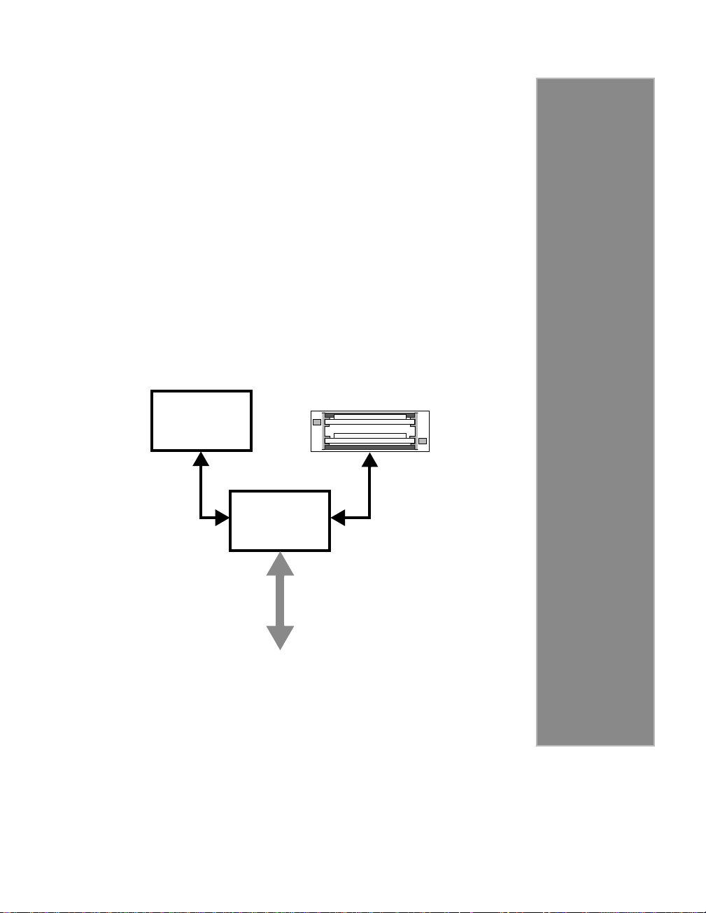
PCMCIA Interface 7
The PCMCIA inteface is controlled by a custom
designed ASIC (application specific integrated
circuit), the TS102. The TS102 provides support for
two PCMCIA cards and, in addition, an interface
between the CPU and microcontroller subsystem
which provides battery management, keybaord and
mouse interfacing, and initial power sequencing
control. The TS102 also provides interfaces for an
external keyboard and mouse, but these are not used
in the SPARCbook 3 application.
PCMCIA
µController
77
TS102
SBus
Figure 7-1 PCMCIA Interface Architecture
Page 84
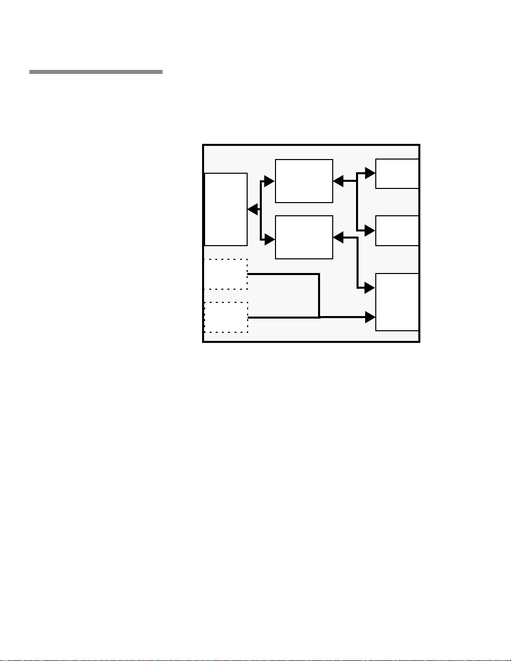
7.1 TS102 Architecture Overview
The general architecture of the TS102 ASIC is illustrated in Figure 8-5.
TS102 Architecture Overview
7.1.1 SBus interface
Bus Sizing
and FIFO
SBus
Interface
Registers
Keybord
Port
Mouse
Port
Card A
Interface
Card B
Interface
µController
Interface
Figure 7-2 TS102 Architecture
The TS102 provides an IEEE-P1496 compliant 32-bit slave interface, with
separate address spaces for PCMCIA memory accesses and for register
accesses. This feature allows user processes access to the PCMCIA
memory resources while restricting access to key systems resources, such
as the microcontroller communications link.
7-2 PCMCIA Interface
The TS102 slave interface supports all SBus transfer sizes up to 8-word
transfers, but not 16-word and extended transfer modes. The TS102
performs the required number of accesses to the PCMCIA interface to
fulfill any request. For example, if the controller requests a 32-bit (word)
access, and the card installed is 16 bit, then the TS102 performs two
accesses.
The TS102 supports posted writes to PCMCIA cards of up 8 words. Such
posted completed by the TS102 after the transfer has been acknowledged
on the SBus. Until the write is complete, further accesses to the TS102
rerun by the TS102.
Page 85

TS102 Architecture Overview
The TS102 also features a read-ahead capability. Setting the read-ahead bit
in the TS102 card register causes the TS102 to pre-fetch an additional 8
words a of data after each 8 word read from the card, starting from the
address used in the last transfer. The address used for subsequent PCMCIA
I/O cycles as a result of a single SBus transaction may be static or
incrementing.
The TS102 supplies a single interrupt request to the CPU. This interrupt
request combines requests from the PCMCIA card interface and the
microcontroller interface. Status registers allow the CPU to determine the
source of the interrupt.
7.1.2 PCMCIA interface
The SPARCbook 3 complies to PCMCIA standards which define the
mechanical and electrical specifications for a wide range of removable
memory and I/O cards. However, there is no provision in the PCMCIA
specification for a DMA master on a PCMCIA card.
The PCMCIA interface supports three memory spaces. These are common
memory space, attribute memory space and I/O space. Common memory
space is intended for simple read-write data memory; attribute memory
typically contains the card configuration registers; and I/O space is used by
I/O cards, such as network interface and modem cards.
The transfer cycle time is either fixed, for release 1.0 compatible cards, or
is determined by the card itself via a WAIT line, for release 2.0 compatible
cards. All card types and slots default to a common memory configuration
at power up or following removal of a card. When a card is installed, the
host interrogates the card through attribute memory to determine whether
any I/O pin functions need to be redefined or whether card operating or
programming voltages require adjustment.
A number of PCMCIA cards request low power 3.3 Volts operation via
their attribute memory data, or request two different programming voltages
for use by programmable memory. The TS102 provides bit-ports, which are
used to select the appropiate voltages, as required. However, because some
signals are shared between the two PCMCIA cards, it is not possible to
operate one card at 3.3V while simultaneously operating the other card at
5V.
7.1.3 Microcontroller interface
A simple 8-bit parallel read-write port supports communications with the
microcontroller subsystem. The CPU writes commands to a transmit
register. The act of writing sets a busy bit in the microcontroller parallel
PCMCIA Interface 7-3
Page 86

port status register, and also asserts an interrupt request to the
microcontroller. The microcontroller read of the receive register clears the
CPU write busy bit and the interrupt request.
There is a similar protocol for transfers from the microcontroller to the
CPU. For improved performance, there is a four entry FIFO in each
direction, which allows posted write cycles to be performed.
7.2 TS102 Memory Mapping
The TS102 occupies a 256 Mbyte region of the SPARCbook 3’s address
space. Its internal memory map is summarized in Table 8-4.
Address Resource
0x40000000 - 0x41FFFFFF FCode PROM
0x42000000 - 0x43FFFFFF TS102 registers
0x44000000 - 0x44FFFFFF Attribute space, card A
0x45000000 - 0x45FFFFFF Attribute space, card B
0x46000000 - 0x46FFFFFF I/O space, card A
0x47000000 - 0x47FFFFFF I/O space, card B
0x48000000 - 0x4BFFFFFF Common memory space, card A
0x4C000000- 0x4FFFFFFF Common memory space, card B
TS102 Memory Mapping
7.2.1 Acceses to PCMCIA Resources
The low order SBus address lines S_A(25:0) are passed directly through to
PCM_A(25:0), permitting access to the full 64Mbyte of common memory
address space. For attribute memory and I/O space, PCM_A(25:24) are
driven from paging bits in the TS102’s register set.
The TS102 accepts byte, halfword, word, doubleword, quadword, and
octalword transfer requests, and responds with error acknowledgment on
request for other sizes.
The TS102 detects the WAIT signal from any card that drives it. This can
be used to extend the transfer cycle on memory and I/O accesses. The wait
can be asserted for up to 12µs which is longer than the maximum 255 SBus
clocks (10.2µs @ 25MHz) allowed for an SBus transfer. If a PCMCIA card
7-4 PCMCIA Interface
Table 7-1 TS102 Address map
Page 87

TS102 Memory Mapping
7.2.2 Byte Swapping
asserts its WAIT signal, the TS102 slave interface responds with a retry
acknowledgment to the master, and then continues with the PCMCIA
transfer cycle.
Similarly, burst accesses to slow PCMCIA cards can cause a single burst
access to take longer than 10µs, and in these cases the TS102 responds with
a retry acknowledgment. The TS102 checks subsequent cycles by
comparing the address, size and direction to ensure that the new cycle is the
retried cycle, and not a new and different cycle. Any other new cycle
attempted to the PCMCIA slave interface must be rerun as it cannot be
attempted until after the retried PCMCIA cycle is complete.
The TS102 supports programmable byte-swapping, to allow the use of big
or little-endian PCMCIA cards. The two PCMCIA card interfaces in the
TS102 have individually programmable byte swapping, although it is not
advisable to program the two differently.
Four byte-swapping modes are implemented in the data routing block of the
TS102, of which three are are of interest here. They are dependent upon the
transfer size, and the two status bits per card indicating the byte ordering
mode. One status bit provides endian control for the normally big-endian
SBus interface, and the other status bit provides endian control for the
PCMCIA card. The details of these modes are shown in theTable 7-2. Data
on the left is the SBus data, and data on the right is the PCMCIA data.
Size
Byte D[31:24] <-> D[7:0] D[31:24} <-> D[7:0] D[31:24] <-> D[7:0] D[31:24] <-> D[7:0]
Halfword D[31:16] <-> D[15:0] D[31:24] <-> D[7:0]
Word D[31:0] <-> D[31:0] D[31:24] <-> D[7:0]
SBus BE
PCMCIA LE
Table 7-2 Sbus to PCMCIA Data Routing
SBus LE
PCMCIA LE
D[23:16] <-> D[15:8]
D[23:16] <-> D[15:8]
D[15:8] <-> D[23:16]
D[7:0] <-> D[31:24]
Sbus BE
PCMCIA BE
D[31:24] <-> D[7:0]
D[23:16] <-> D[15:8]
D[31:24] <-> D[7:0]
D[23:16] <-> D[15:8]
D[15:8] <-> D[23:16]
D[7:0] <-> D[31:24]
SBus LE
PCMCIA LE
D[31:16] <-> D[15:0]
D[31:0] <-> D[31:0]
Accesses to the I/O and attribute spaces are handled differently. The
attribute space is byte wide and only even addressed bytes exist, while
accesses to I/O space must be treated as bytes unless the I/O card responds
PCMCIA Interface 7-5
Page 88

with an IOIS16* acknowledgement. The TS102 monitors the IOIS16*
signal during I/O accesses in order to decide how many PCMCIA accesses
to perform for a given master cycle.
7.2.3 SLAVIO expansion interface
The SLAVIO controls access to the boot EPROM and parallel port. It also
has an expansion bus that allows additional I/O devices to be added. This
expansion bus consists of an 8-bit data path, controlled by the SLAVIO,
and a 20-bit address bus. To support posted write cycles, this address bus
requires an external address latch . This latch is implemented in the TS102.
The expansion bus has a single “generic” chip select. The TS102 uses this,
together with some high order address lines, to select the boot PROM, or
and modem controller. There are three additional selects but these are not
used in the SPARCbook 3. The address map of the decode is shown Table
7-3.
A[19:17] Select
0 x x Boot ROM
1 0 0 Spare
1 0 1 Modem
1 1 0 Interrupt register
1 1 1 Spare
TS102 Memory Mapping
7-6 PCMCIA Interface
Table 7-3 Generic Chip Select Decoding
The boot PROM is placed on the expansion bus because the SLAVIO only
permits read accesses to the EPROM in its conventional location. However,
because the boot PROM is a FLASH device, it is necessary to have write
access to it so that can be reprogrammed in circuit. The TS102 takes the
normal boot PROM select from the SLAVIO and ORs this with the decode
of the generic select to produce a composite PROM select.
The FLASH device implements a software write protection to enhance with
a hardware protection mechanism, in which the TS102 only generates a
boot PROM select for a write cycle if the microcontroller has enabled
EPROM write cycles in a command register in the TS102.
Generation of the boot PROM selects by the TS102 also allows the
implementation of a boot PROM redirection facility. When in operation,
the mechanism inhibits generation of an PROM select and passes the
memory access to the PCMCIA card in slot A. Thus the CPU reads code
from the PCMCIA memory instead of the boot EPROM. This feature is
Page 89

TS102 Registers
intended primarily for recovery from accidental erasure of the boot PROM
contents, but may also be used for such applications as field diagnostics, or
even OS upgrades.
It is also necessary to inhibit the generation of the SBus select to the
SLAVIO device when boot redirection is used, in order to prevent the
SLAVIO from from responding to accesses that are intended for the
PCMCIA interface, while still allowing access to all other SLAVIO
resources. When redirection is selected, the TS102 inhibits the SLAVIO
select if a decode of the SBus physical address indicates that the SLAVIO
would normally direct the cycle to the boot PROM.
7.3 TS102 Registers
There are two separate register blocks within the TS102. The first gives
access to PCMCIA card specific resources, and the second gives access to
the microcontroller interface. Table 7-4 summarizes the TS102’2 register
address map.
0x42000000 Card A Interrupt Register
0x42000004 Card A Status Register
0x42000008 Card A Control Register
0x4200000C Not used
0x42000010 Card B Interrupt Register
0x42000014 Card B Status Register
0x42000018 Card B Control Register
0x4200001C Not used
0x42000020 Microcontroller Interrupt Register
0x42000024 Microcontroller Data Register
0x42000028 Microcontroller Status Register
0x4200002C - 0x4200003C Not used
Address Function
Table 7-4 CPU Register Address Map
All registers are 16 bits wide and are can be read or written.
PCMCIA Interface 7-7
Page 90

The PCMCIA specification relies on software negotiation between the host
system and each card to configure the hardware interface. As a result of this
negotiation, some signals on the PCMCIA interface can, if required, be
redefined. This is handled via the TS102 register interface.
7.3.1 Card A and B interrupt registers
There is one 16 -bit interrupt register for each card. Each register contains
an interrupt status (read) and clear (write) bits and an interrupt mask bit for
each of four interrupt sources.
The request bit is the logical AND of the status and the mask bit, and
indicates that an interrupt is being requested. The mask bits allow masking
of individual interrupts. An interrupt is enabled when the mask is set to 1
and is cleared by writing a 1 to the associated clear bit.
The card interrupt registers also contain the soft reset flag. Setting this bit
to 1 will cause the SPARCbook 3 to be reset.
Bit Read Write
0 IRQ request Clear IRQ request
1 WP status changed request Clear WP status changed request
2 Battery status changed request Clear Battery status changed
3 Card detect status changed
request
4 IRQ status Not used
5 WP status changed status Not used
6 Battery/card status changed status Not used
7 Card detect status changed status Not used
8 IRQ mask IRQ mask
9 WP status mask WP status mask
10 Battery/card status mask Battery status mask
11 Card detect status mask Card detect status mask
12 Soft reset Soft reset
13 Not used Not used
14 Not used Not used
15 Not used Not used
TS102 Registers
Clear card detect status changed
7-8 PCMCIA Interface
Table 7-5 Card Interrupt Register
Page 91

TS102 Registers
I/O cards replace the two battery voltage signals with card status changed
and audio waveform input signals. In this case the battery status changed
interrupt becomes a card status changed interrupt, and the card status must
then be read from the card.
7.3.2 Card status register
The card status register contains card status and control bits.
Bit Name Function Asserted Reset
0 PRES Card is present 1 0
1 IO Card is memory or I/O 1 0
2 TYP3 Card is type 3 (disk) 1 0
3 Vcc Vcc voltage control 0
5:4 Vpp1[1:0] Vpp1 voltage control 00
7:6 Vpp2[1:0] Vpp2 voltage control 00
8 WP Write protect status 1 0
10:9 BVD[1:0] Battery voltage detect
11 LVL Card IRQ interrupt level/edge
12 RDY Card ready/not busy status 1 0
13 Vccen Card Vcc enable 0 0
14 RIEN Ring indicate enable 1 0
15 ACEN Card access enable 1 0
1 0
control
Table 7-6 Card Status Register
Bit 15 ACEN – Card Access Enable
Accesses to the card are enabled when this bit is set (1)
Bit 14 RIEN – Ring Indicator Enable.This is no longer supported.
Bit 13 VccEN – Vcc enable. When this bit is cleared (0) power is
enabled to the card.
Bit 12 RDY – Card ready/not busy status. This bit indicates the
status of the card RDY/BSY* signal. Note that this signal
becomes IREQ* on I/O cards, and the RDY/BSY* status
may be available in the card pin replacement register, if this
bit is implemented in it. Since the RDY/BSY* signal and
IREQ* are one and the same, it is possible to generate an
interrupt on BSY* becoming asserted, since the interrupt
PCMCIA Interface 7-9
Page 92

TS102 Registers
request is not automatically masked when the card is not
I/O. The interrupt request should normally be explicitly
masked when the card is not I/O using the interurpt mask bit
in the card interrupt register.
Bit 11 LVL – IRQ Leve/Edge Control. This bit controls whether
the card IRQ input is edge or level sensitive. By default it is
edge sensitive.
0 = edge sensitive
1 = level sensitive
Bits 10:9 BVD(1:0) – Battery Voltage Detect. These bits indicate the
status of the card battery voltage detect bit. These are not
valid for an I/O card, and the battery voltage status may be
read from the card pin replacement register, if these bits are
implemented in the card.
00 = battery low, data suspect
01 = battery low, data suspect
10 = battery low, data OK
11 = battery good
Bit 8 WP – Write Protect. The WP bit indicates that the card is
write protected, as the card has its WP signal asserted.
7-10 PCMCIA Interface
Bits 7:6 Vpp2(1:0) – Programming Voltage Control
Bits 5:4 Vpp1(1:0) – Programming Voltage Control. The Vpp1 and
Vpp2 bits control the Vpp1 and Vpp2 voltages, and allow
them to be set to:
00 = 0V
01 = Vcc (5V or 3.3V)
10 = Vpp (12V)
11 = NC
Bit 3 Vcc – The Vcc bit controls the card Vcc voltage, allowing it
to be set to either 5V or 3.3V:
0 = 5V
1 = 3.3V
Bit 2 TYP3 – The TYP3 bit configures the card as a disk. This
may not be implemented if Type-3 PCMCIA data is not
available.
Bit 1 IO – The IO bit controls whether the card is configured for
I/O or memory:
Page 93

TS102 Registers
0 = Memory card
1 = I/O card
Bit 0 PRES – Present. The PRES bit indicates that both card
detects are active and that the card is correctly inserted.
7.3.3 Card Control Register
Bit Name Function Asserted Reset Comments
1:0 AA[25:24] Attribute address A(25:24)
3:2 IA[25:24] I/O address A(25:24) 00
6:4 CES[2:0] CE/address setup time 111 000 = 1 clocks
001 = 2 clocks
010 = 3 clocks
011 = 4 clocks
100 = 5 clocks
101 = 6 clocks
110 = 7 clocks
111 = 8 clocks
9:7 OEW[2:0] OE/WE width 111 000 = 2 clocks
001 = 3 clocks
010 = 4 clocks
011 = 5 clocks
100 = 6 clocks
101 = 7 clocks
110 = 8 clocks
111 = 9 clocks
10 CEH Chip enable hold time 1 0 = 1 clocks
1 = 2 clocks
11 SBLE SBus little endian 1 0 1 indicates SBus operation in ‘lit-
tle’ endian mode
12 PCMBE PCMCIA big endian 1 0 1 indicates PCMCIA interface
should be ‘big’ endian
13 RAHD Read ahead enable 1 0 Set to 1 to enable read-ahead
14 INCDIS Address increment disable 1 0 Set to 1 to disable PCMCIA
address incrementing in I/O
PCMCIA accesses from SBus
15 PWRD Power down 1 0 Set to 1 to power down
Table 7-7 Card Control Register
PCMCIA Interface 7-11
Page 94

7.3.4 Microcontroller Interrupt Register
Bit Name Function Asserted Reset
0 TXE_REQ Transmit FIFO empty inter-
rupt request
1 TXNF_REQ Transmit FIFO not full inter-
rupt request
2 RXNE_REQ Receive FIFO not empty
interrupt request
3 RXO_REQ Receive FIFO overflow inter-
rupt request
4 TXE_MSK Transmit FIFO empty mask 1 0
5 TXNF_MSK Transmit FIFO not full mask 1 0
6 RXNE_MSK Receive FIFO not empty
mask
7 RXO_MSK Receive FIFO full mask 1 0
Table 7-8 Microcontroller Interrupt Register
7.3.5 Microcontroller data register
Microcontroller Registers
1 0
1 0
1 0
1 0
1 0
Bit Read Write
D[7:0] Data from microcontroller Data to microcontroller
7.3.6 Microcontroller status register
Bit Name Function Asserted Reset
0 TXE_STA Transmit FIFO empty status 1 1
1 TXNF_STA Transmit FIFO not full status 1 1
2 RXNE_STA Receive FIFO not empty sta-
3 RXO_STA Receive FIFO overflow status 1 0
Table 7-10 Microcontroller Status Register
7.4 Microcontroller Registers
7-12 PCMCIA Interface
Table 7-9 CPU Data Register
1 0
tus
Page 95

Microcontroller Registers
The microcontroller has access to TS102 registers within its own address
space. The content of these registers and protocols for use are under the
control of software programmed into the microcontroller’s onboard ROM
during system manufacture.
The registers within the microcontroller’s address space are shown in the
table below.
Address Function
0x00 Host data register
0x01 Host interrupt register
0x02 Host status register
0x03 Not used
0x04 Command register
0x05-0x07 Not used
0x08 Keyboard data register
0x09 Keyboard interrupt status register
0x0A Keyboard status/control register
0x0B Not used
0x0C Mouse data register
0x0D Mouse interrupt status/control register
0x0E Mouse status register
0x0F Not used
Table 7-11 Microcontroller register set
PCMCIA Interface 7-13
Page 96

Microcontroller Registers
7-14 PCMCIA Interface
Page 97
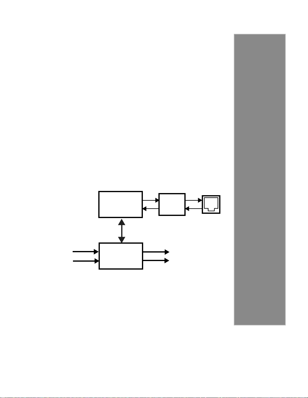
ISDN and 16-bit Audio 8
The ISDN and 16-bit Audio interfaces on the
SPARCbook 3 are provided by a pair of coupled
components: the AT&T T7259 Dual Basic Rate
ISDN Controller (DBRI); and the Crystal
Semiconductor Corporation CS4215 Multimedia
Audio Coder-Decoder (CODEC). These provide a
terminal endpoint (TE) ISDN interface at the S/T
reference point, and also high quality stereo audio.
The architecture of the ISDN and audio interface is
illustrated in Figure 8-1.
88
ISDN
DBRI Chip
Concentration
Highway
Interface
Stereo Line-In
Mono Microphone
Figure 8-1 ISDN and Audio Interface
Audio
CODEC
ISDN
Terminal
Endpoint
Protection
Stereo Line-Out
Stereo Headphones
ISDN
I/O Panel
Connector
Page 98

8.1 ISDN Overview
The integrated services digital network (ISDN) is an advanced telephone
system which allows computers to communicate together at a higher data
rate than they could using a modem. Information carried on the ISDN is
digital and uses a circuit switched system at a basic rate of 64 KB/s on each
of two bearer channels, or B channels, and 16 KB/s on a signaling and
control channel, or D channel. The B channels can be combined to provide
a maximum throughput of 128 KB/s.
The ISDN interface on SPARCbook 3 provides a 4-wire terminal endpoint
(TE) connection via an RJ45 connector on the I/O panel, providing transmit
and receive differential signal pairs. This is connected to the ISDN at the S
(or S/T) interface point. Signals at the S point are then converted by an
adapter called a network termination (NT1) to use the more common two
wire telephone connection for which most premises are currently wired.
The connection can be point to point between an NT1 and TE or multipoint,
with up to eight TE devices attached to a single NT1. These eight devices
may share a single ISDN line to achieve virtually simultaneous operation.
Time division multiplexing is employed to superimpose both B channels
and D channel together onto a differential wire pair. The data carried on the
B channels is arbitrary and could contain digitized voice and picture
information, or raw computer data. A collision detection and backoff
strategy allows multiple TEs to share the D channel for control and
signaling functions.
ISDN Overview
Basic rate ISDN uses a 48-bit frame and defines several time slots within
the frame. Among these are the D channel and two B channels. There are
additional bits of information which are required by the physical layer
electronic circuits to support the framing, synchronization and multipoint
capabilities of ISDN.
8.2 DBRI Overview
The the AT&T T7259 Dual Basic Rate ISDN Controller (DBRI) functions
as a multiport tap into an ISDN line and has four ports through which data
is passed. In addition to the synchronous serial TE port, there is an NT port
(not used in SPARCbook 3), a serial Concentration Highway Interface
(CHI) port, and the 32-bit SBus DMA port. In general, the DBRI is a digital
data transport, formatter and multiplexer that dynamically routes bits
within time slots between ports.
8-2 ISDN and 16-bit Audio
Page 99
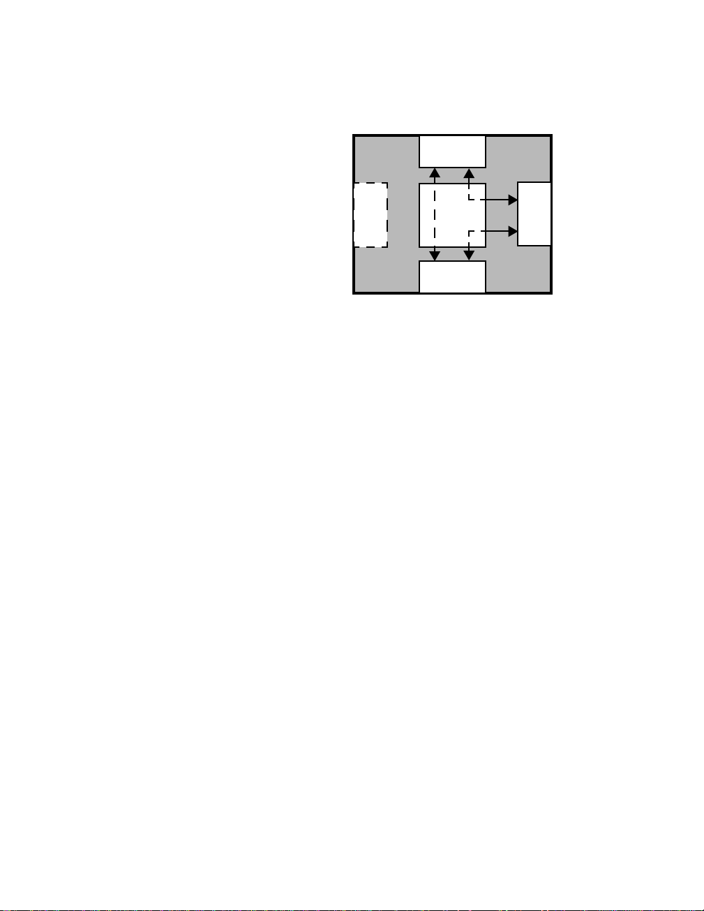
DBRI Overview
SBus
Interface
Figure 8-2 DBRI Internal Architecture
8.2.1 TE and NT Ports
The TE port provides the basic network connection to the ISDN. The NT
port is not used in SPARCbook 3.
An internal FIFO buffer is used as a pipe to hold data transfering between
interfaces. Data is moved between the various ports by assigning pipes and
time slots to connect them. The D channel input and output streams use the
High Data Level Link Control (HDLC) protocol, as required by ISDN.
Once a connection is made through a pipe, little or no service is required to
maintain it other than to manage buffer pools of data received and for
transmission.
8.2.2 CHI Port
The CHI port is used to connect the audio CODEC. It provides a
synchronous serial link which is used to transfer frames of audio data
between the DBRI and audio CODEC. The CHI uses four wires to
communicate: the data transport clock (CHIK); a frame synchronization
pulse (CHIFS); a data transmit data wire; and a receive data wire. Data
frames exchanged between the two devices contain digital audio or control
information. Specific time slots within each frame are assigned to carry
particular types of data.
NT
TE
CHI
8.2.3 SBus Interface
The 32-bit bus port is a fully compliant SBus DMA master that supports up
to 64-byte DMA bursts. Up to sixteen pipes, each 80 bytes long, can be used
to support DMA operations.
ISDN and 16-bit Audio 8-3
Page 100
8.2.4 DBRI Programming Model
This section gives a brief overview of the DBRI programming interface. It
is not, however, intended to provide a detailed programming guide.
The DBRI operates as a coprocessor, maintaining its own data structures in
memory and operating on its own instruction set. The host assembles lists
of instructions, services interrupts and maintains receive and transmit data
buffers in main memory. The DBRI accesses memory using DMA
operations.
The DBRI can be configured to select time slots and route selected data
between the three serial interfaces and the SBus. It can be dynamically
reconfigured to provide different routing strategies for different operations.
For example, audio data carried on one B channel from the TE interface
could be routed through the CHI for audio output, while data on the other
B channel could be routed to the SBus interface for DMA into main
memory. Figure 8-3 shows this configuration
B1 Slots
DBRI Overview
Long Pipe
Short Pipe
B2 Slots
From TE
DMA to Memory
To CHI for Audio Output
Figure 8-3 Long and Short Pipes
Data Pipes The DBRI provides 32 data pipes through which data is channelled
between the interfaces. These are divided into two types: sixteen long data
pipes, so called because they have enough depth to buffer data for DMA (80
bytes); and sixteen short data pipes of 32 bits each. The long data pipes can
be used for DMA with optional HDLC formatting in either direction. The
short data pipes are used for data transfer between two serial interfaces
(CHI, NT, and TE) and can have time slots assigned to both ends.
8-4 ISDN and 16-bit Audio
 Loading...