

Page 1

User Manual
8020
20 MHz Programmable
Function Generator
PUBLICATION DATE: April 15, 2007
Copyright 2001 by Tabor Electronics. All rights reserved. This book or parts thereof may not be reproduced in
any form without written permission of the publisher.
Tabor Electronics Ltd.
9 Hatasia Street, Tel Hanan, Israel 20302
TEL: (972) 4 821 3393, FAX: (972) 4 821 3388
[www.taborelec.com]
REVISION: D
Page 2

Warranty
Tabor Electronics’ products are warranted against defects in material and workmanship, when
used under normal operating conditions, for a period of one year after delivery. Tabor
Electronics will repair or replace without charge any product which proves defective during
this period. Repair necessitated by misuse of the product is not covered by this warranty. No
other warranties are expressed or implied, including but not limited to the implied warranties
of merchantability and fitness for a particular purpose. Tabor Electronics is not liable for
consequential damage.
REPAIR AND CALIBRATION
Prior authorization is required from Tabor Electronics before products are returned for service.
All service must be performed by Tabor Electronics’ factory or an authorized service center.
Please contact the factory directly for repair and re-calibration:
Tabor Electronics, Ltd.
9 Hatasia Street
Tel Hanan, Israel 20302
Tel: 972-4-821-3393
Fax: 972-4-821-3388
Page 3

Tabor Electronics Ltd.
REPAIR AND CALIBRATION REQUEST FORM
To allow us to better understand your repair requests, we suggest you use
the following outline when calling and include a copy with your instrument
to be sent to the Tabor Repair Facility.
Model
Serial No. Date
Company Name
Purchase Order #
Billing Address
City
State/Province Zip/Postal Code Country
Shipping Address
City
State/Province Zip/Postal Code Country
Technical Contact Phone Number ( )
Purchasing Contact
Phone Number ( )
1. Describe, in detail, the problem and symptoms you are having. Please include
all set up details, such as input/output levels, frequencies, waveform details, etc.
2. If problem is occurring when unit is in remote, please list the program strings used
and the controller type.
3. Please give any additional information you feel would be beneficial in facilitating
a faster repair time (i.e., modifications, etc.)
4. Is calibration data required? Yes No (please circle one)
Call before shipping Ship instruments to nearest support office
Note: We do not accept Iisted on back.
“collect” shipments.
Page 4

Safety Precautions
The following safety precautions should be observed before using this product and associated
computer. Although some instruments and accessories would normally be used with non-hazardous voltages, there are situations where hazardous conditions may be present. This product
is intended for use by qualified personnel who recognize shock hazards and are familiar with
the safety precautions required to avoid possible injury. Read the operating information
carefully before using the product. Exercise extreme caution when a shock hazard is present.
Lethal voltage may be present on cables, connector jacks, or test fixtures.
The American National Standard Institute (ANSI) states that a shock hazard exists when
voltage levels greater than 30V RMS, 42.4V peak, or 60 VDC are present. A good safety
practice is to expect that hazardous voltage is present in any unknown circuit before touching
or disconnecting the line cord. Before operating an instrument, make sure the line cord is
connected to a properly grounded power receptacle. Inspect the connecting cables and test
leads for possible wear, cracks, or breaks before each use.
For maximum safety, do not touch the product, test cables, or any other of the instrument parts
while power is applied to the circuit under test. ALWAYS remove power from the entire test
system before connecting cables or jumpers, installing or removing cards from the computer,
or making internal changes, such as changing card address. Do not touch any object that could
provide a current path to the common side of the circuit under test or power line (earth) ground.
Always keep dry hands while handling the instrument. If you are using test fixtures, keep the
lid closed while power is applied to the device under test. Safe operation requires that the
computer lid be closed at all times during operation.
Carefully read the Safety Precautions instructions that are supplied with your computer.
Instruments, cables, leads or cords should not be connected to humans. Before performing any
maintenance, disconnect the line cord and all test cables. Finally, maintenance should be
performed by qualified service personnel only. If you have no past experience in instrument
servicing, we strongly recommend that installation and initial tests on the instrument be done
by your dealer or by the factory itself.
Page 5

DECLARATION OF CONFORMITY
We: Tabor Electronics Ltd.
9 Hatasia Street, Tel Hanan
ISRAEL 20302
declare, that the 50 MHz Pulse/Function Generators
Model 8020 and Model 8021
meet the intent of Directive 89/336/EEC for Electromagnetic Compatibility and complies with the
requirements of the Low Voltage Directive 73/23/EEC. Compliance was demonstrated to the following
specifications as listed in the official Journal of the European Communities:
Safety:
EN 61010-1
IEC 1010-1 (1990) + Amendment 1 (1992)
EMC:
EN 50081-1 Emissions:
EN 55022 - Radiated, Class B
EN 55022 - Conducted, Class B
EN 50082-1 Immunity:
IEC 801-2 (1991) - Electrostatic Discharge
IEC 801-3 / ENV50140 (1993) - RF Radiated
IEC 801-4 (1991) - Fast Transients
Model 8020 and Model 8021 were tested in typical configuration.
Page 6

Model 8020 Table of Contents
TABLE OF CONTENTS
SECTION 1. GENERAL INFORMATION
1-1 Introduction 1-1
1-2 Description 1-1
1-3 Instrument and Manual Identification 1-2
1-4 Options 1-2
1-5 Specifications 1-2
1-6 Safety Consideration 1-2
1-7 Accessories Supplied 1-2
SECTION 2. INSTALLATION
2-1 Introduction 2-1
2-2 Unpacking and Initial Inspection 2-1
2-3 Performance Checks 2-1
2-3 Power Requirements 2-1
2-5 Grounding Requirements 2-1
2-6 Installation and Mounting 2-2
2-7 Bench Operation 2-2
2-8 Rack Mounting 2-2
2-9 Portable Use 2-2
2-10 Short Term Storage 2-2
2-11 Long Term Storage or Repacking for Shipment 2-2
2-12 Safety 2-3
SECTION 3. OPERATION
3-1 Introduction 3-1
3-2 Front Panel Familiarization 3-1
3-2-1 Controls 3-1
3-2-1-1 Status 3-1
3-2-1-2 Display/Modify 3-1
3-2-1-3 Trigger Mode 3-3
3-2-1-4 Operating Mode 3-3
3-2-1-5 Output 3-3
3-2-1-6 Modifier 3-3
3-2-2 Connectors 3-3
3-2-3 Display And Indicators 3-4
Page -1
Page 7

Model 8020 Table of Contents
3-3 Rear Panel Familiarization 3-4
3-3-1 Connectors and Switches 3-4
3-4 Power-up Procedure 3-4
3-5 Software Reset 3-5
3-5-1 Parameter Preset 3-5
3-6 Display Messages 3-6
3-7 Detecting Programming Errors 3-6
3-7-1 General Error 3-6
3-7-2 Pulse/Ramp Set-up Errors (model 8021 only) 3-6
3-7-3 Offset Errors 3-6
3-7-4 IEEE-488 Errors 3-7
3-8 Selecting 2nd Functions 3-7
3-9 Modifying Parameters 3-7
3-9-1 Modifier 3-8
3-9-2 Range 3-8
3-9-3 Parameter Limits 3-8
3-10 Selecting an Output Waveform 3-9
3-11 Disabling The Output 3-9
3-12 Selecting an Operating Mode 3-9
3-12-1 Function Generator Mode 3-9
3-12-2 Sweep Generator Mode 3-9
3-12-2-1 Selecting Sweep Direction 3-9
3-12-3 Voltage Controlled Oscillator Mode 3-10
3-12-4 Pulse Generator Mode (model 8021 only) 3-10
3-12-5 AM Mode (model 8022 only) 3-11
3-13 Triggering The Pulse Generator 3-11
3-14 Using Front Panel Set-ups 3-11
3-14-1 Store Set-ups 3-11
3-14-2 Recall Set-ups 3-12
3-14-2-1 Using The Recall Mode 3-12
3-15 Using The Offset 3-12
3-16 Changing The GPIB Address 3-12
SECTION 4. IEEE PROGRAMMING
4-1 Introduction 4-1
4-2 Bus Description 4-1
4-3 IEEE-488 Bus Lines 4-2
4-3-1 Bus Managment Lines 4-2
4-3-2 Handshake Lines 4-2
4-3-3 Data Lines 4-3
4-4 Interface Function Codes 4-3
4-5 Software Considerations 4-4
4-6 Hardware Consideration 4-4
Page -2
Page 8

Model 8020 Table of Contents
4-6-1 Typical Controlled Systems 4-4
4-6-2 Connections 4-5
4-7 Changing GPIB Address 4-5
4-8 Bus Commands 4-5
4-8-1 Uniline Commands 4-6
4-8-2 Universal Multiline Commands 4-7
4-8-3 Addressed Commands 4-8
4-8-4 Unaddress Commands 4-9
4-8-5 Device Dependent Commands 4-9
4-8-6 Common Commands and Queries 4-9
4-9 Device Listing Formats 4-9
4-9-1 Function Element Summary 4-10
4-9-2 Seperator Function Element Summary 4-10
4-9-2-1 Program Message Unit Seperator 4-10
4-9-2-2 Program Data Seperator 4-10
4-9-2-3 Program Header Seperator 4-10
4-9-3 Program Message Terminator 4-11
4-9-4 Command Program Header 4-11
4-9-5 Query Program Header 4-11
4-9-6 Program Data 4-11
4-9-6-1 Character Program Data 4-11
4-9-6-2 Decimal Numeric Program Data 4-11
4-9-6-3 Suffix Program Data 4-12
4-9-6-4 Non-Decimal Program Data 4-12
4-9-6-5 Arbitrary Block Program Data 4-12
4-9-6-6 Expression Program Data 4-12
4-10 Device-Dependent Command Programming 4-12
4-10-1 Display Modify (D) 4-12
4-10-2 Operating Mode (P,V,A,O) 4-16
4-10-3 Trigger Mode (G,T) 4-16
4-10-4 Output Mode (C,B) 4-16
4-10-5 Waveform (U) 4-16
4-10-6 Parameter Programming 4-16
4-10-7 Common Commands 4-17
4-10-7-1 Set-ups (*SAV, *RCL) 4-18
4-11 Device Talking Formats 4-18
4-11-1 Function Element Summary 4-19
4-11-2 Seperator Function Element Summary 4-19
4-11-2-1 Response Message Unit Seperator 4-19
4-11-2-2 Response Data Seperator 4-19
4-11-2-3 Response Header Seperator 4-19
4-11-3 Response Message Terminator 4-19
4-11-4 Response Header 4-20
4-11-5 Response Data 4-20
Page -3
Page 9

Model 8020 Table of Contents
4-11-5-1 Character Response Data 4-20
4-11-5-2 Decimal Numeric Response Data 4-20
4-12 Reading From the Model 8020 4-20
4-12-1 Interrogate Parameter Data Query 4-21
4-12-2 Common Queries 4-21
4-12-3 Response Header (X) 4-21
4-12-4 Response Message Terminator 4-22
4-13 Device Status Reporting 4-22
4-14 Status Byte Register 4-22
4-14-1 Reading the Status Byte Register 4-23
4-14-1-1 Reading with a Serial Poll 4-23
4-14-1-2 Reading with the *STB? 4-23
4-14-1-3 Clearing the Status Byte Register 4-23
4-14-1-4 Service Request Enable Register 4-23
4-14-2 Standard Event Status Register (ESR) 4-24
4-14-2-1 Standard Event Status Register (ESE) 4-24
4-14-3 Machine Status Register (STT) 4-26
4-15 Front Panel Error Messages 4-26
4-15-1 ILI (Illegal Instruction) Error 4-26
4-15-2 ILP (Illegal Parameter) Error 4-26
SECTION 5. MAINTENANCE AND PERFORMANCE CHECKS
5-1 Introduction 5-1
5-2 Line Voltage Selection 5-1
5-3 Fuse Replacement 5-1
5-4 GPIB Interface Option Field Installation (option 1) 5-1
5-4-1 Option 1 Installation Procedure 5-2
5-5 Disassembly Instructions 5-2
5-6 Special Handling Of Static Sensitive Devices 5-3
5-7 Cleaning 5-3
5-8 Repair and Replacement 5-3
5-9 Performance Checks 5-3
5-9-1 Environmental Conditions 5-3
5-9-2 Warm-up Period 5-3
5-9-3 Recommended Test Equipment 5-3
5-10 Performance Checks Procedure 5-4
5-10-1 Frequency - Gated Mode 5-4
5-10-2 Frequency - Continuous Mode 5-4
5-10-3 Amplitude 5-5
5-10-4 DC Characteristics 5-5
5-10-5 Squarewave Characteristics 5-5
5-10-6 Sine Characteristics 5-5
Page -4
Page 10

Model 8020 Table of Contents
5-10-7 Sine Flatness 5-6
5-10-8 Trigger, Gate, Manual 5-6
5-10-9 Sweep 5-6
5-10-10 VCO Control 5-7
5-10-11 Pulse Width (model 8021) 5-7
5-10-12 Amplitude Modulation (model 8022) 5-8
SECTION 6. THEORY OF OPERATION
6-1 Introduction 6-1
6-2 Overall Functional Description 6-1
6-3 Analog Circuitry 6-1
6-3-1 Current Generator 6-1
6-3-2 Voltage controlled Oscillator 6-3
6-3-3 Sine Shaper 6-4
6-3-4 Trigger Circuit 6-4
6-3-5 Pulse Shaper 6-6
6-3-6 Preamplifier 6-7
6-3-7 Attenuator 6-7
6-3-8 Offset Generator 6-7
6-3-9 Power Amplifier 6-7
6-3-10 Post Amplifier Attenuator 6-7
6-3-11 Power Supply 6-7
6-4 Pulse Generator Circuit (model 8021) 6-7
6-5 AM Circuit (model 8022) 6-9
6-6 Digital Circuitry 6-9
6-6-1 Display and Keyboard Interface 6-9
6-6-2 Counter Circuit 6-10
6-6-3 IEEE-488 Interface (Option 1) 6-10
SECTION 7. ADJUSTMENTS
7-1 Introduction 7-1
7-2 Adjustments 7-1
7-2-1 Environmental Conditions 7-1
7-2-2 Warm-up Period 7-1
7-2-3 Recommended Test Equipment 7-1
7-2-4 Adjustment Procedures 7-1
7-3 Adjustment Procedure 7-2
7-3-1 Power Supply Adjustment 7-2
7-3-2 Distortion Adjustment 7-2
7-3-3 Frequency Adjustment 7-2
7-3-4 Low Frequency Adjustment 7-2
7-3-5 Low Frequency Distortion Adjustment 7-2
Page -5
Page 11

Model 8020 Table of Contents
7-3-6 Trigger Start Phase Adjustment 7-3
7-3-7 Amplitude Adjustment 7-3
7-3-8 Offset Adjustment 7-3
7-3-9 Squarewave Response Adjustment 7-3
7-3-10 Sine Flatness Adjustment 7-3
7-3-11 Triangle Flatness Adjustment 7-4
7-3-12 Reference Oscillator Adjustment 7-4
7-3-13 Pulse Width Adjustment (model 8021 only) 7-4
7-3-14 Ramp Amplitude Adjustment (model 8021 only) 7-4
7-3-15 Amplitude Modulation Adjustment 7-4
SECTION 8. PARTS LIST
8-1 General 8-1
8-2 Ordering Information 8-1
8-3 Maintenance Kit 8-1
8-4 Parts Description 8-1
SECTION 9. SCHEMATIC DIAGRAMS
LIST OF TABLES
1-1 Model 8020 Specifications 1-3
3-1 Default State After Software Reset 3-5
3-2 Offset Amplitude Programming Limits 3-7
3-3 Front Panel Parameter Entry Limits 3-8
4-1 Model 8020 Interface Function Codes 4-4
4-2 IEEE contact Designation 4-5
4-3 IEEE-488 Bus Command Summary 4-6
4-4 Default conditions. (Status after SDC or DCL) 4-8
4-5 Device Dependent Command Summary 4-10
4-6 SRQ Mask Commands 4-13
4-7 SRQ Mask Legal Commands 4-13
5-1 Line Fuse Selection 5-1
5-2 Required Test Equipment 5-4
8-1 Model 8020 Parts List - Main Board assembly 8-1
8-2 Model 8020 Parts List - Final Amplifier Board Assembly 8-4
8-3 Model 8020 Parts List - Front Panel Board Assembly 8-7
8-4 Model 8021 Parts List - Pulse Generator Board Assembly 8-7
8-5 Model 8022 Parts List - AM Generator Board Assembly 8-8
Page -6
Page 12

Model 8020 Table of Contents
LIST OF FIGURES
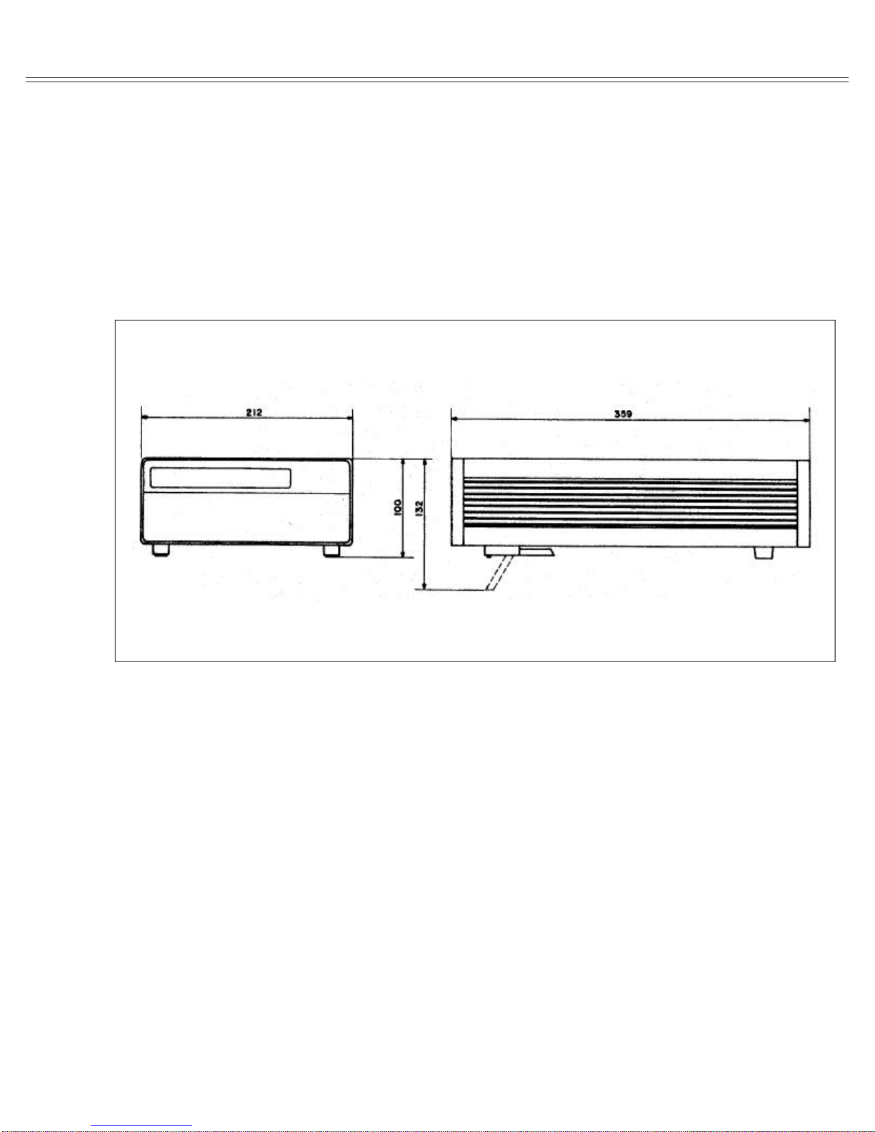
2-1 Model 8020- Outline Dimensions 2-3
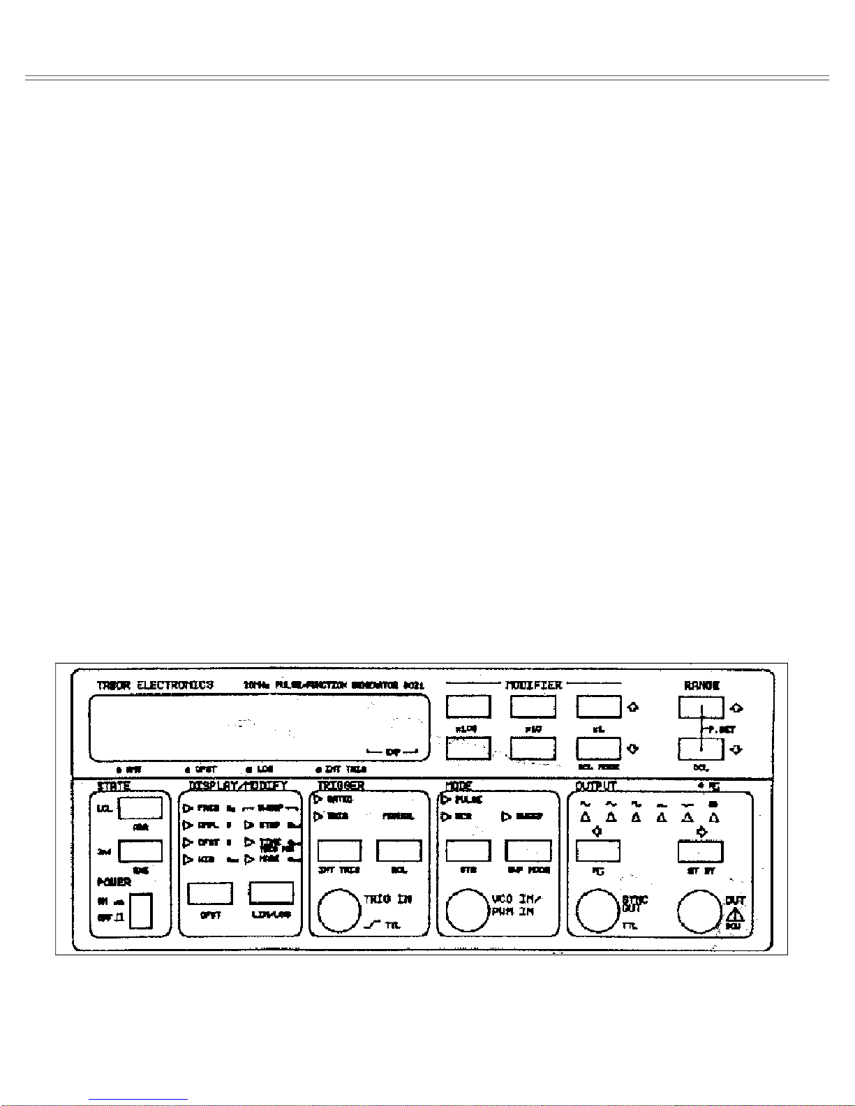
3-1 Front Panel Controls, Indicators and Connectors 3-2
4-1 IEEE Bus Configuration 4-2
4-2 IEEE Handshake Sequence 4-3
4-3 IEEE-488.2 Status Reporting Model 4-25
5-1 GPIB Interface Option Installation 5-2
6-1 Model 8020- Simplified Block Diagram 6-2
6-2 Current Generator Simplified Block Diagram 6-3
6-3 VCO Simplified Block Diagram 6-4
6-4 Model 8020 - Clamp Circuit Simplified Diagram 6-5
6-5 Model 8020 - Clamp Circuit Waveform (Triggered Mode) 6-5
6-6 Model 8020 - Clamp Circuit Waveform (Gated Mode) 6-6
6-7 Pulse Generator Functional Block Diagram 6-8
6-8 AM Functional Block Diagram 6-9
Page -7
Page 13

Model 8020 Table of Contents
This page was intentionally left blank
Page-8
Page 14

Model 8020 General Information
SECTION 1
GENERAL INFORMATION
1-1. INTRODUCTION
This manual provides operation and maintenance information for the Model 8020 Function Generator. Section 1
is a general description of the Model 8020. Sections 2 and
3 contain installation and operation instructions. IEEE
programming is explained in Section 4. Maintenance and
performance checks are provided in section 5. The theory
of operation is described in section 6. Section 7 outlines
calibration and troubleshooting procedure. Section 8 contain tables of replaceable parts and recommended spare
parts. Section 9 contains schematic and component location diagrams.
1-2. DESCRIPTION
Model 8020 is a high performance - digital function generator. It provides a variety of signal waveforms, for use as
test stimuli to many different electronic devices. Microprocessor based, Model 8020 is extremely easy to set up
for manual use as well as simple to program in an IEEE488 GPIB system environment. The generator features as
standard: lin/log sweep, pulse waveforms and complete
triggering facilities - including internal trigger generator.
Model 8020 provides a wide frequency coverage and a
large amplitude span; ensuring continuing usefulness for
a variety of tasks, today as well as in the future, when demands change. Rapid, repeatable testing every time is assured by thirty non-volatile stored set-ups thus, ensuring
exact duplication of previous set-ups no matter how complex is assured. Its performance, programmability and
economy make it equally at home in every laboratory.
Output may be selected to be either continuous, gated
or triggered. The function generator features a built-in
trigger generator which can replace an external triggering
device. Additional convenience is achieved through the
MANUAL button permitting user control over triggering
sequences.
Alternately, model 8020 may also be used as an independent sweep generator with its output signal swept over
an exceptionally wide range of 10 decades. A choice of
eight sweep modes, both linear and logarithmic, covers
most applications which are known today. A MARKER
output is provided to permit Z-axis modulation of an oscilloscope to intensify parts of the scope trace.
Output level ranges from 20 mV to 30 Vp-p into open
circuit or 10 mV to 15 Vp-p into 50 ohms. Maximum DC
offset plus AC signal is variable within a window level
from -15 V to +15 V into open circuit or from -7.5 V to +7.5
V into 50 ohms.
The function generator employs a built-in counter.
This counter is not available to the outside world however,
it is incorporated in an internal loop which automatically
monitors the output frequency. When a deviation of more
than a few tenth of a percent is detected by the counter, the
frequency is automatically corrected by the internal microprocessor.
There are two other models which will be described in
this manual:
Model 8021 - 20 MHz Pulse/Function Generator.
This instrument is identical in its basic functions to the
Model 8020. In addition, this instrument offers Pulse and
Ramp capabilities. Pulse width and ramp width ranges are
controllable within a range of 25.0 nS to 9.99 S. Pulse complement and inverted ramp functions are also available.
Model 8022 - 20 MHz AM Function Generator. This
model offers an amplitude modulation function in addition to the 8020 functions. Carrier level is controllable
within the range of 0 to 100 %. Modulating signal is applied through a front panel BNC connector. The operator
may select as a carrier any of the standard available functions.
Page 1-1
Page 15

General Information Model 8020
NOTE
1-5. SPECIFICATIONS
This manual provides a complete description
of all features of the 8020 series. Therefore,
several of the features which are described in
the following paragraphes may not be installed in your instrument.
1-3. INSTRUMENT & MANUAL IDENTIFICATION
The serial number of the instrument is located on the rear
panel of the instrument. The two most significant digits
identify instrument modifications. If this prefix differs
from that listed on the title page of this manual, there are
differences between this manual and your instrument.
Technical corrections to this manual (if any) are listed
in the back of this manual on an enclosed MANUAL
CHANGES sheet.
1-4. OPTIONS
Model 8020 offers a GPIB interface bus option; designated as OPTION 1.
Option 1 is field installable or may be ordered with new
instruments from the factory. Installation procedures are
given in Section 6 of this manual. There are no software
modifications necessary when installing the option. The
instrument will automatically sense the presence of the
newly installed interface and will then permit operation
through the IEEE-488 GPIB interface.
Instrument specifications are listed in Tables 1-1. These
specifications are the performance standards or limits
against which the instrument is tested.
NOTE
All specifications in the following table apply
with output terminated with 50 feedthrough
termination and with an amplitude of 15Vp-p.
Warm-up period is 30 min at an ambient temperature of 25 +/-5 deg C.
1-6. SAFETY CONSIDERATIONS
Model 8020 is a Safety Class 1 instrument with an exposed
metal chassis that is directly connected to earth via the
power supply cable and has been manufactured according
to international safety standards. Before the instrument is
switched on, make sure that protective earth terminal is
connected to a protective earth via the power cord. Do not
remove instrument covers when operating or when power
cord is connected to mains.
Any adjustment, maintenance and repair of the opened
instrument under voltage should be avoided as much as
possible, but when inevitable, should be carried out only
by a skilled person who is aware of the hazard involved.
1-7. ACCESSORIES SUPPLIED
Page 1-2
The 8020 is supplied with ac power cord and with an instruction manual. Extra manual is available on request.
Page 16

Model 8020 General Information
Table 1-1. Model 8020 Specifications
WAVEFORMS:
FREQUENCY CHARACTERISTICS
Range: 2 mHz to 20 MHz
Resolution: 3 1/2 digits (2000 counts max) with exponent
Accuracy:
Continuous: +/-3 % of full scale from 2 mHz to 9.99 Hz; .1 % of full scale from 10 Hz to 20MHz
VCO and Gated: +/-3 % of reading to 2.000 MHz; +/-5 % of reading to 20 MHz
Jitter: <0.1 % 50 pS
WAVEFORM CHARACTERISTICS
Sinewave Total harmonic distortion:
Harmonic signals: >25 db below the carrier level from 1 MHz to 20 MHz
Triangle Linearity: Better than 99% up to 100 KHz (measured between 10% to 90% of amplitude)
Squarewave, Pulse:
Rise/Fall time: <12 nS (10 % to 90 % of amplitude)
Abberation: <5 %
TTL Pulse:
Rise/Fall time: <25 nS
Sine, Triangle, Square, Positive Pulse, Negative Pulse, TTL Pulse (SYNC out), DC
<1 % from 2 mHz to 20.0 Hz
<.5 % from 20 Hz to 100 KHz
<1 % from 100 KHz to 1 MHz
OUTPUT CHARACTERISTICS
Stand-by mode: Output Normal or Disabled, selectable
Impedance: 50 ohms +/-2 %
Output Level: 20.0 mV to 30.0 V p-p into open circuit; 10.0 mV to 15.0 V p-p into 50 ohms
Resolution: 2 1/2 digits (150 counts) with exponent
Accuracy (1 KHz): +/-2 % of reading from 1.0 V to 15.0 V
+/-3 % of reading from .10 V to 1.50 V
+/-4 % of reading from 10 mV to 150 mV
Vernier Control: Continuous throughout the output level
Output Protection: protected against continuous short to case ground.
Flatness (sine): <0.5 db to 1 MHz; <1.5 db to 20 MHz
Offset Resolution: 3 digits with exponent
Offset Range: Offset and amplitude are independently selectable within the following window levels:
Window Amplitude Offset Offset
Level Range Accuracy
+/-7.50 V 1.0E 0 -15.0E 0 0E 0 - 7.00 E 0 1% +/-(1% of Ampl + 40mV)
+/-2.37 V 48E 0 - 150E 0 0E 0 - 2.13 E 0 2% +/-(1% of Ampl + 10mV)
+/-750mV .10E 0 - .47E 0 0E-3 - 700 E-3 2% +/-(1% of Ampl + 4mV)
+/-237mV 10E-3 - 150E-3 0E-3 - 232 E-3 3% +/-(1% of Ampl + 1mV)
Page 1-3
Page 17

General Information Model 8020
Table 1-1. Model 8020 Specifications (continued)
DC CHARACTERISTICS
Range: Variable from -15 V to + 15V into open circuit;
Resolution: 3 digits (750 counts max) with exponent
Accuracy: +/-(1% of reading +20 mV) to 7.50 V;
TRIGGERING CHARACTERISTICS
Source: Manual front panel push button, external TRIG IN or internal trigger generator
Modes:
Normal: Continuous waveform is generated
External Trigger: Each input cycle generates a single output cycle
Internal Trigger: An internal timer repeatedly generates a single output cycle
Gated: External signal enables generator. First output cycle synchronous with active slope of triggering
External Rate: To 20 MHz
Ext. Trigger Level: TTL
Int. Trigger Period: Continuously adjustable from 10 S to 1000 S
Slope: Positive going leading edge
LOGARITHMIC SWEEP CHARACTERISTICS
(models 8020 & 8022)
-7.5 V to +7.5 V into 50 ohms
+/-(2% of reading +2 mV) to 750 mV
signal. Last cycle of output waveform always fully completed
Modes: Auto, Manual, Triggered and Gated sweep. Main frequency, when triggered, repeatedly
changes from frequency set by the frequency start to frequency set by the sweep
stop setting. Frequency will sweep up, down, or up-down depending on the relationship between the sweep start and sweep stop set-ups and the selected sweep
mode
Width: 10 decades maximum
Rate per Decade: continuously adjustable from 10 mS to 1000 S (nominal) per decade
Steps per decade: Depends on sweep time and range. Automatically adjusted by the instrument to get the
maximum steps per sweep time. Maximum steps are 200; minimum steps are 50
Sweep Output: 2 V/decade for decades; 1 V/decade for 5 decades
Marker Output: 0 V with no marker; drops to approx -5 V when marker frequency is reached. Remains -5 V
from the marker frequency to the end of the sweep
Sweep Stop Resolution: Same as frequency resolution
LINEAR SWEEP CHARACTERISTICS
Modes: Same as in logarithmic sweep
Sweep Width: 3 decades maximum
Sweep Time: continuously adjustable from 10 mS to 1000 S (nominal)
Sweep Out: 0 to 10 V +/-5%
Sweep Steps: Depends on sweep time and range. Automatically adjusted by the instrumentto get the
maximum steps per sweep time. Maximum steps are 1000; minimum steps are 16
Page 1-4
Page 18

Model 8020 General Information
Table 1-1. Model 8020 Specifications (continued)
Marker Output: Same as logarithmic sweep
Sweep Stop Resolution: Same as Frequency resolution
VOLTAGE CONTROLLED OSCILLATOR (VCO) CHARACTERISTICS
Input Impedance: 10 Kohms +/-5 %
Sensitivity: 0 V to -10 V +/-20 % produces frequency change 1/1000 from main frequency when
main frequency is set to 2000 counts
Bandwidth: DC to 70 KHz
FM Sensitivity: 0 V to 100 mV modulates to 1% deviation from center frequency
PULSE / RAMP CHARACTERISTICS - MODEL 8021
Pulse Modes: Symmetrical Pulse, Positive Pulse, Negative Pulse and Complement
Pulse Width Range: 25.0 nS to 9.99 S
Max Duty Cycle: 90 % (limited by 25 nS dead time)
Ramp Modes: Positive Going Ramp, Negative Going Ramp
Ramp Width Range: 5.00 uS to 9.99 S
Max Frequency: 150 KHz
Max Duty Cycle: 90 % (limited by 1 uS dead time)
Resolution: 3 digits with exponent
Accuracy: +/-3 % +/-4 nS 25.0 nS to 99.9 mS; +/-10 % 100 mS to 9.99 S
PWM (pulse width modulation):
Mode: External PWM
Input: Via front panel PWM IN BNC connector
Input Impedance: 10 Kohms +/-5 %
Sensitivity: +/-5 V produces >10 % pulse width change when instrument is set to 100 counts
AM CHARACTERISTICS - MODEL 8022
Mode: External AM
Input: Via front panel AM IN BNC connector
Input Impedance: 10 Kohms +/-5 %
Carrier:
Waveform: All available front panel waveforms
Level Range: Continuously adjustable from 0 % to 100 % (100 % carrier level is proportional to one
half of the programmed amplitude level)
Resolution: 3 digits (100 counts max)
Distortion: <1 % at 70 % modulation (Measured with Fc = 1 MHz and Fm = 1 KHz)
Modulating Signal:
Bandwidth: DC to 500 KHz (DC coupled)
Sensitivity: 0 V to 2.5 Vp-p produces 0 % to 100 % modulations respectively when carrier is set to 100
%; 0 V to 5 Vp-p produces suppressed carrier amplitude modulation (SCAM)
having an output amplitude level of 0 V to 15 Vp-p into 50 ohms respectively
when carrier is set to 0 %
Page 1-5
Page 19

General Information Model 8020
Table 1-1. Model 8020 Specifications (continued)
GPIB INTERFACE (IEEE-488-1978) - Option 1
Programmable controls: All front panel controls except POWER switch; Output may be disabled through
a bus command
Subsets: SH1, AH1, T6, TE0, L4, LE0, SR1, RL1, PP2, DC1, DT1, C0
Data Output Format: Fixed output format consisting of 15 or 17 ASCII characters plus terminators
Data Input Format: ASCII characters lower or upper case. ASCII characters smaller than 20 HEX (32) are
ignored except CR (0D HEX)
Service Request: Selectable for illegal commands, illegal parameters and error
String Termination: Selectable CR, LF, EOI or combination of all.
Address Selection: Front panel programming. Address is stored in a non-volatile memory
ENVIRONMENTAL
Operating temperature: 0 deg C to 40 deg C ambient
Specified Accuracy: +25 deg C +/-5 deg C
Storage temperature: -40 deg C to +70 deg C
Humidity range: 80% R.H
GENERAL
Display: 4 digits 7 segment LEDs 14.2mm high with automatic decimal point, exponent and polarity
indicators
Power: 115/230 Vac +/- 10 %, 50 or 60 Hz, 50 VA max
Stored Settings: 30 complete sets of front panel control settings. The previous control settings and GPIB ad-
dress are stored in a non-volatile memory. Storage guaranteed for 24 month
Dimensions: 87 x 210 x 390 mm (H x W x L)
Weight: Approximately 5 Kg
Page 1-6
Page 20

Model 8020 Installation
SECTION 2
INSTALLATION
2-1. INTRODUCTION
This section contains information and instructions necessary for the installation and shipping of the function generators - 8020 series. Details are provided for initial inspection, power connection, grounding safety requirements, installation information, and re-packing instructions for storage or shipment.
2-2. UNPACKING AND INITIAL INSPECTION
Unpacking and handling of the counter requires only the
normal precautions and procedures applicable to the handling of sensitive electronic equipment. The contents of all
shipping containers should be checked for included accessories and certified against the packing slip to ascertain
that the shipment is complete.
2-3. PERFORMANCE CHECKS
The instrument was carefully inspected for mechanical
and electrical performance before shipment from the factory. It should be free of physical defects and in perfect
electrical order upon receipt. Check the instrument for
damage in transit and perform the electrical procedures
outlined in Section 5. If there is indication of damage or
deficiency, see the warranty in this manual and notify your
local Tabor field engineering representative or the factory.
CAUTION
It is recommended that the operator be fully
familiar with the specifications and all sections of this manual. Failure to do so may compromise the warranty and the accuracy which
Tabor has engineered into your instrument.
2-4. POWER REQUIREMENTS
The function generator may be operated from any one of
the following sources: a. 103.5 to 126.5 Volts (115 Volts
nominal) b. 207 to 253 Volts (230 Volts nominal).
The instrument operates over the power mains frequency range of 48 to 63 Hz. Always verify that the operating power mains voltage is the same as that specified on
the rear panel voltage selector switch.
CAUTION
Failure to switch the instrument to match the
operating line voltage will damage the instrument and may void the warranty.
The Model 8020 should be operated from a power
source with its neutral at or near ground (earth potential).
The instrument is not intended for operation from two
phases of a multiphase ac system or across the legs of a
single-phase, three-wire ac power system. Crest factor
(ratio of peak voltage to rms) should be typically within the
range of 1.3 to 1.6 at 10% of the nominal rms mains voltage.
2-5. GROUNDING REQUIREMENTS
To insure the safety of operating personnel, the U.S.
O.S.H.A. (Occupational Safety and Health) requirement
and good engineering practice mandate that the instrument panel and enclosure be “earth” grounded. All Tabor
instruments are provided with an Underwriters Laboratories (U.L. and V.D.E) listed three-conductor power cable,
which when plugged into an appropriate power receptacle, grounds the instrument. The long offset pin on the
male end of the power cable carries the ground wire to the
long pin of the Euro connector (DIN standard) receptacle
on the rear panel of the instrument.
To preserve the safety protection feature when operating the instrument from a two-contact outlet, use a threeprong to two-prong adapter and connect the green lead on
the adapter to an “earth” ground.
Page 2-1
Page 21

Installation Model 8020
CAUTION
To avoid operator shock hazard do not exceed
the power mains voltage frequency rating
which limits the leakage current between case
and power mains. Never expose the instrument to rain, excessive moisture, or condensation.
2-6. INSTALLATION AND MOUNTING
The instrument is fully solid state and dissipates only a
small amount of power. No special cooling is required.
However, the instrument should not be operated where the
ambient temperature exceeds 40 deg C, when the relative
humidity exceeds 80% or condensation appears anywhere
on the instrument. Avoid operating the instrument close to
strong magnetic fields which may be found near high
power equipment such as motors, pumps, solenoids, or
high power cables. Use care when rack mounting to locate
the instrument away from sources of excessive heat or
magnetic fields. Always leave 4 cm (1.5 inches) of ventilation space on all sides of the instrument.
2-7. BENCH OPERATION
2-11. LONG TERM STORAGE OR
RE-PACKAGING FOR SHIPMENT
If the instrument is to be stored for a long period or shipped,
proceed as directed below. If you have any questions contact your local Tabor field engineering representative or
the Tabor Service Department at the factory.
If the original Tabor supplied packaging is to be used
proceed as follows:
1. If the original wrappings, packing material, and container have been saved, re-pack the instrument and accessories originally shipped to you. If the original container is
not available, one may be purchased through the Tabor
Service Department at the factory.
2. Be sure the carton is well sealed with strong tape or metal
straps.
3. Mark the carton with the model number and serial
number with indelible marking. If it is to be shipped, show
sending address and return address on two sides of the box;
cover all previous shipping labels.
If the original container is not available, proceed as fol-
lows:
The Model 8020 is shipped with plastic feet, tilt stand in
place and ready for use as a bench or portable instrument.
See outline drawing Figure 2-1 for dimensions.
2-8. RACK MOUNTING
The instrument may be rack mounted in a standard 19 inch
rack. The instrument may be rack mounted in Rack Mount
Kit option 8020-rack.
2-9. PORTABLE USE
The instrument may be used in applications requiring portability. A tilt stand consisting of two retractable legs is provided with each unit.
2-10. SHORT TERM STORAGE
If the instrument is to be stored for a short period of time
(less than three months), place cardboard over the panel
and cover the instrument with suitable protective covering
such as a plastic bag or strong craft paper. Place power cable and other accessories with the instrument. Store the
covered voltmeter in a clean dry area that is not subject to
extreme temperature variations or conditions which may
cause moisture to condense on the instrument.
1. Before packing the unit, place all accessories into a plastic bag and seal the bag.
2. For extended storage or long distance shipping only, use
U.S. government packing method II C and tape a two-unit
bag of desiccant (per MIL-D-3464) on the rear cover.
3. Place a 13 cm (5 inch) by 30 cm (12 inch) piece of sturdy
cardboard over the front panel for protection.
4. Place the counter into a plastic bag and seal the bag.
5. Wrap the bagged instrument and accessories in one inch
thick flexible cellular plastic film cushioning material
(per PPP-C-795) and place in a barrier bag (per MIL-B-
131). Extract the air from bag and heat seal.
6. Place bagged instrument and accessories into a 250 mm
(10 inch) x 360 mm (14 inch) x 508 mm (20 inch) fiber
board box (per PPP-B-636 type CF, class WR, variety SW,
grade V3C). Fill additional spaces with rubberized hair or
cellular plastic cushioning material. Close box in accordance with container specifications. Seal with sturdy water
resistant tape or metal straps.
7. Mark container “DELICATE INSTRUMENT”,
“FRAGILE”, etc. Mark instrument model and serial
number and date of packaging. Affix shipping labels as
required or mark according to MIL-STD-129.
Page 2-2
Page 22
Model 8020 Installation
NOTE
RETURN AUTHORIZATION NUMBER
If the instrument is to be shipped to Tabor for
calibration or repair, attach a tag to the instrument identifying the owner. Note the problem, the symptoms, and service or repair desired. Record the model and serial number of
the instrument. Show the work authorization
order as well as the date and
method of shipment. ALWAYS OBTAIN A
2-12. SAFETY
FROM THE FACTORY BEFORE SHIP-
PING THE INSTRUMENT TO TABOR.
Be fully acquainted and knowledgeable with all aspects of
this instruction manual before using the instrument to assure operator safety and protection against personnel
shock hazard. hazard.
Figure 2-1. Model 8020 - outline dimensions.
Page 2-3
Page 23

Installation Model 8020
This page was intentionally left blank
Page 2-4
Page 24

Model 8020 Operating Instructions
SECTION 3
OPERATING INSTRUCTIONS
3-1. INTRODUCTION
Model 8020 operation is divided into two general categories: basic bench operation, and IEEE-488 operation.
Basic bench operation, which is covered in this section,
explains how to use the model 8020 for generating the
required waveform characteristics. IEEE programming
(with option 1 installed) can also be used to greatly enhance the capability of the instrument in applications
such as automatic test equipment. This aspect is covered
in details in Section 4.
3-2. FRONT PANEL FAMILIARIZATION
The front panel layout of the Model 8020 is shown in Figure 3-1. The front panel is generally divided into three
sections: controls, connectors, display and indicators.
The following paragraphs describe the purpose of each
of these items in details.
3-2-1. Controls
All front panel controls except POWER are momentary
contact switches. Most controls include an annunciator
light for indication of the selected parameter and operating mode. Some controls do not have an annunciator
light. Exercising these controls generates an immediate
response on the display.
Front panel controls may be divided into functional
groups: Status, Display/Modify, Trigger Mode, Operating mode, Output and Modifiers.
3-2-1-1. Status
Three push-button are included in the status group. The
function of each of these buttons is described in the following.
POWER
the instrument. Pressing and releasing the switch once
turns the power on. Pressing and releasing the switch a
second time turns the power off.
- The POWER switch controls the AC power to
2nd/EXE - Several push-buttons were assigned a second
function which are only accessible after the [2nd] button
was depressed. These functions are market below the
buttons in yellow script. Some second functions require
that the [2nd] push-button be pressed again before the
function is executed.
- The LOCAL push-button when pressed, and the
LCL
instrument is in its remote mode (but not in remote lockout condition LLO), restores the instrument to its local
operating mode. When the generator is in local operating
mode, pressing this push-button generates no response.
A 2nd function is assigned to this switch. Depressing this
push-button after the [2nd] button modifies the numeric
read-out to display the programmed GPIB address.
3-2-1-2. Display/Modify
There are two DISPLAY/MODIFY push-buttons which
are use for modifying the displayed reading. Each time a
button is depressed a different parameter is displayed.
The selected parameter is indicated by an LED. The dimensions which are associated with each parameter are
located below the numeric display. The following parameters may be displayed and modified:
FREQ - Frequency of the selected output waveform.
Frequency is defined for repetitive signals only. When
the function generator is set to operate in triggered mode,
the programmed frequency value has no effect on the
output. In gated mode, the frequency defines the repetition rate within the gating signal. In sweep mode, the programmed value defines the sweep start point. The programmed frequency retains its value at both SYNC and
the main output connectors.
AMPL
output connector. The output signal is driven from a 50
ohms source therefore, the value of the amplitude parameter is specified and accurately controlled only when
the output is terminated with 50 ohms. If the signal from
the output connector is connected to an high impedance
circuit, the actual amplitude level at the output connector
- Amplitude of the selected waveform at the main
Page 3-1
Page 25
Operating Instructions Model 8020
is doubled. Amplitude control has no effect on the amplitude level at the SYNC output connector.
OFST - DC offset of the selected waveform at the main
output connector. Similarly to the amplitude, the offset
parameter is specified and accurately controlled only
when the output is terminated with 50 ohms. Offset control has no effect on the SYNC output connector.
WID - (Model 8021 only) The width parameter is common to the pulse and the ramp waveforms. When the
function generator is set to operate in pulse mode, this
parameter specifies the pulse width at the output connector. When the instrument is set to operate in ramp mode,
this parameter specifies the ramp width at the output connector.
In pulse mode, the pulse width parameter defines the
time interval between two consecutive transitions; positive to negative transition in normal output mode or negative to positive transition in pulse complement mode.
The displayed and specified value is that obtained at the 50
% of amplitude setting.
The definition of ramp width is a little more complicated because the edges are less defined. In this case the
specified and displayed ramp width value is that obtained
by the turn point of the edges - positive to negative turning
points in positive ramp output or negative to positive turning points in negative ramp output.
CARR - (Model 8022 only) Carrier defines the amplitude of the output waveform signal when the function
generator is set to operate in its AM mode and when no
modulating signal is applied to the EXT. AM input connector. The carrier level is specified as percentage of the
programmed amplitude value where 100 % carrier is
equivalent to 50 % of the displayed amplitude level.
The carrier signal is driven from a 50 ohms source
therefore, the value of the carrier parameter is specified
and accurately controlled only when the output is terminated with 50 ohms. If the signal from the output connector is connected to an high impedance circuit, the actual
carrier level at the output connector is doubled. Carrier
control has no effect on the amplitude level at the SYNC
output connector.
STOP - Defines the sweep stop frequency. When the
function generator is set to operate with one of its sweep
modes, the waveform at the output connector sweeps
from frequency set by the FREQ setting to that set by the
stop frequency. In several sweep modes sweep stop may
change its function to sweep start. The programmed frequency retains its value at both SYNC and the main output connectors.
TIME - In linear sweep mode, sweep time determines
the time that it takes for completing one sweep cycle.
Sweep time is different for logarithmic sweep mode
where the specified value is that required for sweeping
one decade. The generator may be set to sweep over 10
decades. In that case, the sweep time should be multiplied by ten. Decade size ranges from 200 to 1999 counts
(or 20:1 if settings other than full and minimum scales
are required). If only part of the decade is being swept,
the sweep time is reduced proportionally.
Figure 3-1. Front Panel Controls, Indicators and Connectors
Page 3-2
Page 26

Model 8020 Operating Instructions
MARK - Specifies the frequency of which the sweep
marker changes its voltage level at the marker output
connector. The marker output is only active when the
function generator is set to operate with one of its built-in
sweep modes.
TRIG PER - A built-in generator provides an internal
triggering stimulant in such cases where an external signal is not available. The displayed value specifies the
interval between consecutive triggering sequences.
Table 3-2 lists the limits for each of the above parameters.
3-2-1-3. Trigger Mode
Two push-buttons are grouped in the TRIGGER MODE
section. Selection of one of the trigger modes is done by
depressing one of these buttons. The selected mode is indicated by an LED. Model 8020 may be triggered from
either one of the following sources:
1. External signal which may be applied to the TRIG IN
connector
2. An internal - asynchronous trigger generator
3. GPIB commands (like GET)
4. Front panel [MANUAL] push-button
The [MANUAL] trigger is active when the instrument
set to operate in its external trigger mode. This push-button when depressed serves as a replacement for an external
trigger source.
3-2-1-4. Operating Mode
Two push-buttons are available at the operating mode
group. Selection of one of the operating modes is done
by depressing one of these buttons. The selected mode is
indicated by an LED.
Model 8020 may operate in several operating mode
such as sweep or VCO modes. Model 8021 provides two
additional modes: pulse and PWM. Model 8022 provides
additional amplitude modulation mode.
3-4-1-5. Output
There are two push-buttons in the OUTPUT group.
These buttons are used for selecting an output waveforms for the output connector. The selected function is
indicated by an LED.
3-4-1-6. Modifier
The MODIFIER push-buttons simulate digital potentiometers. The MODIFIER push-buttons operate in conjunction with the DISPLAY/MODIFY group. There are
four sets of modifying buttons. Three sets are dedicated
for changing the displayed read-out. One set changes the
range of the displayed parameter.
3-2-2 Connectors
The connectors are used for connecting the Model 8020
to the unit under test and to and to external triggering
source.
1. TRIG INPUT - The TRIG INPUT connector is used
for applying an external triggering source to the function
generator.
2. VCO INPUT - The VCO INPUT connector is used for
applying an external dc voltage source to the function
generator. The same input is used for connecting a pulse
width modulating signal (model 8021 only) or for connecting an amplitude modulating signal (model 8022
only).
2a. VCO/PWM INPUT - The VCO/PWM INPUT
(model 8021 only) connector serves two functions. In
VCO operating mode this input is used for applying an
external dc voltage source to the function generator. The
same input is used for connecting a pulse width modulating signal when the instrument is set to operate in pulse
mode.
2b. VCO/AM INPUT - The VCO/AM INPUT (model
8022 only) connector serves two functions. In VCO operating mode this input is used used for applying an external dc voltage source to the function generator. The
same input is used for connecting an amplitude modulating signal when the instrument is set to operate in its AM
mode.
3. SYNC OUT - The SYNC OUT connector outputs
fixed amplitude pulses from a 50 ohms source. This output is synchronous with the main output.
4. OUTPUT - The OUTPUT connector is used as the
main output for the function generator. Output is driven
from a 50 ohms source. Special care should be taken
when these outputs are connected to the device under test
because these outputs are capable of delivering up to 30
Vp-p.
Page 3-3
Page 27

Operating Instructions Model 8020
3-2-3. Display And Indicators
1. DISPLAY - The function of the numeric display is to
indicate the value of the various parameters. The display
consists of a 4 digit mantissa and a single digit exponent.
The exponent uses a leading minus indicating negative
values. The sign on the exponent changes to + for zero or
positive values. The display is also used for indicating
other information such as messages.
2. DIMENSIONS - Parameter dimensions are located
below the numeric display. there are 3 indicators which,
together with the exponent, are used for determining the
correct value of the displayed parameter.
3. INDICATORS - 24 indicators are located on the front
panel. These indicators are used as pointers to a selected
parameter such as frequency, amplitude and offset or
modes such as gated, triggered and VCO.
3-3. REAR PANEL FAMILIARIZATION
3-3-1. Connectors And Switches
1. AC RECEPTACLE - Power is applied through the
supplied power cord to the 3-terminal AC receptacle.
Note that the selected ac mains voltage is marked on the
line voltage selector switch.
2. LINE SWITCH - The LINE VOLTAGE SELECTOR
switch selects one of the primary voltage which are
marked on both sides of the switch.
3-4. POWER-UP PROCEDURE
The basic procedure of powering up the Model 8020 is
described below.
1. Connect the female end of the power cord to the AC
mains receptacle on the rear panel. Connect the other end
of the power cord to a grounded AC outlet.
WARNING
Be sure the power line voltage agrees with
the indicated value on the rear panel of the
instrument. Failure to heed this warning
may result in instrument damage.
The instrument is equipped with a 3-wire
power cord designed to be used with
grounded outlets. When the proper connections are made, the instrument chassis is
connected to the power line ground. Failure
to use a properly grounded outlet may result
in personal shock hazard.
2. Turn on the mains power by pressing and releasing the
POWER switch on the front panel.
3. The instrument will then begin operation by performing a display and indicator test which takes approximately one second. All front panel indicators will turn on
and the display will appear as follows:
8.8.8.8. 8
3. LINE FUSE - The line fuse provides protection for the
AC power line input. For information on replacing this
fuse, refer to Section 5.
4. IEEE-488 CONNECTOR - This connector is used
for connecting the instrument to the IEEE-488 bus.
5. SWEEP OUT CONNECTOR - This connector is
used for connecting the instrument the X input on the oscilloscope. Its output is either fixed, in linear sweep
mode, or proportional to the sweep time per decade, in
logarithmic sweep mode.
6. MARKER OUTPUT CONNECTOR - This connector is used for connecting the function generator to the Z
input on the oscilloscope. This output is only active
when sweep mode is on.
Page 3-4
4. To verify that all display segments are operating, compare the instrument’s display with the above during the
test.
5. Following the display test, the instrument proceeds by
displaying its model number similar to the following:
8020
6. Once the model number is displayed, the instrument
performs ROM and RAM tests. Successful execution of
these tests is followed by a one second read-out of the
installed software revision similar to the example below:
So 1.0
7. Following the displayed software revision, the instru-
ment proceeds with displaying the installed options.
When no option is installed, the instrument skips this
message. If option 1 (GPIB) is installed, the instrument
displays the following message:
OPt.1
Page 28

Model 8020 Operating Instructions
8. Following the option message, the instrument proceeds with displaying the previously selected GPIB primary address. If GPIB option is not installed the instrument skips this message. The GPIB address is set by front
panel programming and is stored in the non-volatile
memory. For example, with the generator programmed
to address 15, the display will show:
IE15
9. Following these display messages, the instrument will
commence its normal operating mode and begin generating waveforms. Note that the instrument is equipped
with a non-volatile memory. This memory automatically monitors front panel traffic and retains its latest
set-up for events such as accidental power loss. In case of
power loss the instrument resumes operation with its
previously programmed front panel set-up.
It is possible to remove the sequence of displayed messages from the power up procedure by using a built-in shift
function. Depressing [SHIFT] and then [RANGE UP] in
sequence writes a special code to the non-volatile memory. The next time the generator is powered up, the instrument will skip the power up procedure and will immediately commencewith displaying the front panel set-up. repeating the sequence of [SHIFT] and [RANGE UP] restores normal power up procedure. Other shift functions
Table 3-1. Default States After Software Reset
are described later in this section.
3-5. SOFTWARE RESET
One, who is not yet fully familiar with front panel operation of the function generator, may find himself locked
into a “dead-end” situation where nothing operates the
way it should. The fastest way of restoring the generator
to a known state is by resetting its software. This may be
done by pressing the [2nd] push-button and then pressing the [DCL] push-button (second function to the
[RANGE DOWN] push-button). The instrument then
resets to it’s factory selected defaults. Table 3-1 summarizes these defaults.
3-5-1. Parameter Preset
As discussed in paragraph 3-5, software reset places all
front panel parameters at their factory selected defaults.
It may however be required to preset one or two parameters and leave the rest untouched. In that case the instrument provides additional capabilities with its [P.SET]
(preset) function. Depressing simultaneously the
[RANGE UP] and the [RANGE DOWN] push-buttons
modifies the displayed parameter to its preselected default value. Defaults values are summarized in Table 3-
1.
FUNCTION DESCRIPTION DEFAULT STATE
FREQ Frequency 10.00 KHz
AMPL Amplitude 1.00 V
OFST Offset 0.00 V
WID Pulse/Ramp Width 10.0 S
CARR Carrier Level 100 %
STOP Sweep Stop Frequency 2.00 KHz
TIME Sweep Time 1.00 S
T.PER Internal Trigger Period 1.00 S
MARK Sweep Marker Frequency 5.00 KHz
DC AMPL DC Amplitude 0.00 V
2nd Functions OFST Offset Mode Off
LIN/LOG Sweep Mode Linear
INT TRIG Internal Trigger Mode Off
SWP MODE Sweep Mode Sweep up
ST. BY Stand By Off
STATUS IEEE Status Local
DISPLAY/MODIFY Displayed Parameter Frequency
TRIGGER Trigger Mode Continuous
MODE Operating Mode Normal
OUTPUT Output Waveform Sinewave
Page 3-5
Page 29

Operating Instructions Model 8020
NOTE
Software reset has no effect on stored front
panel set-ups in memory locations 00
through 30. Software reset also has no effect
on the programmed GPIB address.
3-6. DISPLAY MESSAGES
Model 8020 has several display messages pertaining to
its operation. The generator also displays an error indication when a front panel programming error is detected.
These messages and error indications are discussed in
the following. Note that the instrument has a number of
additional display messages associated with IEEE-488
programming. These messages are discussed in section
4 of this manual.
3-7. DETECTING PROGRAMMING ERRORS
Model 8020 is a product of many years of experience and
complete understanding of human engineering requirements. During its design stage, a great deal of time was
devoted for simplifying front panel programming procedures, thereby minimizing the potential of programming
errors. It is impossible however for an inexperienced operator to completely avoid some errors. For such cases,
the function generator employs a built-in error detection
mechanism which warns against programming errors.
Errors are categorized in four main groups:
1. General errors
2. Pulse/Ramp setup errors
3. Offset errors
4. IEEE errors
3-7-1. General Errors
parameter every time that a modifier push-button is depressed. Programming the Model 8020 with pulse/ramp
errors is possible and executable however, when such errors are detected, the light next to the selected waveform
starts blinking; indicating that the signal at the output
connector may emerge with other parameters then those
programmed. The light blinks until the error conditions
are removed.
Pulse/Ramp errors may occur under one or more of the
following conditions:
1. The programmed pulse/ramp WID (width) parameter is greater than the selected period (1/FREQ).
2. Model 8021 is placed in sweep mode and the programmed pulse/ramp width parameter is greater than the
selected sweep stop period.
3. Model 8021 is placed in internal triggered mode and
the programmed pulse/ramp width is greater than the selected internal trigger period.
4. The programmed ramp width is outside the limit of
5.00 uS.
5. The programmed ramp frequency is outside the limit
of 150 KHz.
3-7-3. Offset Errors
Normally, the output waveform is used symmetrically
around the 0 V line. This means that with an output voltage of 10 Vp-p and with no offset applied, the lowest
peak reaches -5 V. Consequently, the highest peak
reaches +5 V. The instrument provides an additional
flexibility by using its output waveform in conjunction
wth an offset voltage. It is however, impossible to exceed
the instrument limits. Offset and amplitude are independently selectable within the limits given in Table 3-2.
Errors in this group are caused by improper usage of the
instrument. Such errors occur while attempting to place
the instrument in an illegal mode. For example, depressing simultaneously two push-buttons (except [P.SET])
has no valid definition. In this case, the instrument simply ignores this error and continues with its normal operation.
3-7-2. Pulse/Ramp Set-up Errors (model 8021 only)
The pulse/ramp setup errors are inter-parameter inconsistencies errors, such as pule width greater than the selected period. The pulse generator tests the programmed
Page 3-6
The instrument will reject any attempt to call the
[OFST] function if the sum of the amplitude and the offset
exceeds the specified limits and will display the following
error message on its read-out:
ERR
The function generator then resumes normal operation.
No offset is applied to the output waveform.
Page 30

Model 8020 Operating Instructions
Tabel 3-2. Offset Amplitude Programming Limits
Window Amplitude Offset
Range Range
+/-7.50 V 1.0E 0 -15.0E 0 0E 0 - 7.00 E 0
+/-2.37 V 48E 0 - 150E 0 0E 0 - 2.13 E 0
+/-750 mV .10E 0 - .47E 0 0E-3 - 700 E-3
+/-237 mV 10E-3 - 150E-3 0E-3 - 232 E-3
3-7-4. IEEE-488 Errors
In general, whenever a GPIB programming attempts to
put the model 8020 into an error condition, the function
generator responds in two ways. First by displaying a
front panel message and than, if programmed so, by raising an SRQ flag in its status byte. The controller may then
address the generator using the serial poll command and
request its status byte.
The generator incorporates a number of display messages which are associated with errors involving GPIB interface programming. These messages are discussed in detail in Section 4 of this manual.
There is one message however, which should be explained at this point because it may interfere with front
panel operation. A remote enable or a device dependent
command sent to the instrument through the bus turns the
REMOTE light on. In this case, all front panel push-buttons except [LCL] are disabled. Press one of these pushbuttons causes the function generator to respond with the
following message:
LcL
This message indicates that the instrument expects that
the [LCL] push-button be first depressed otherwise front
panel operation is ignored. After the [LCL] button is depressed, the REMOTE light turns off and the instrument is
ready to accept further front panel programming sequences.
Unless the [LCL] push-button is pressed and the REMOTE light turns off.
3-8. SELECTING 2nd FUNCTIONS
A few front panel push-buttons were assigned a secondary function. These functions are printed in yellow below the button and are accessible through the [2nd] pushbutton.
There are twelve front panel buttons whih were as-
signed a secondary function. These functions are:
ADR STO
EXE SWP MODE
OFST COMPLEMENT
LIN/LOG ST-BY
INT TRIG RCL MODE
RCL DCL
The operation of these secondary functions is described
later in this chapter. Pressing the [2nd] push-button generates the following display read-out:
2nd ?
The question mark (?) appears blinking; indicating
that the instrument is ready for a consequent press of another push-button which was assigned a secondary function. Depressing [2nd] once more cancels this function.
3-9. MODIFYING PARAMETERS
There are various parameters, such as frequency and amplitude, which control the shape of the waveform at the
output connector. Modification of a specific parameter
is simply done by pressing the push-button below the requested parameter until the light next to the required parameter illuminates. At this time the numeric readout
displayed a value plus an exponent. The dimension is
marked on the panel next to each parameter. For exam-
Page 3-7
Page 31

Operating Instructions Model 8020
ple, the FREQ dimension is Hz. Display readout of 10.00
(exp)+3 tells us that the output waveform is programmed
to have a frequency of 10.00 KHz. Limits for each parameter are given in Table 3-3. The parameter is then
modified using the [MODIFIER] and the [RANGE]
push-buttons.
The parameters which can be modified are marked on
the front panel as follows:
FREQ STOP
AMPL WID (model 8021)
TIME CARR (model 8022)
OFST MARK
In addition, some parameters are accessible through the
[2nd] button. These parameters are:
ADR SWP MODE
RCL RCL MODE
STO
3-9-1. Modifier
The modifier group consists of three sets of push-buttons
each set having its top button marked with an arrow
pointing up and its bottom key marked with an arrow
pointing down. These modifier push-button control the
displayed readout within a selected range.
[x1 UP] or [x1 DOWN] push-buttons when depressed
and released once increments or decrements the least sig-
nificant digit on the numeric display. Depressing these
buttons for more than one second modifies this digit constantly until the button is released or until the parameter
limit is encountered. Incrementing the [x1] above 9 carries
1 to the second digit.
The [x10 UP] or [x10 DOWN] push-buttons control
the second digit. Their operation is similar to the [x1] operation. Incrementing the [x10] above 9 carries 1 to the second digit.
The [x100 UP] or [x100 DOWN] push-buttons control
the third and the most significant digit.
3-9-2. RANGE
The [RANGE] buttons control the range of the displayed
parameter. Depressing and releasing the [RANGE UP]
or the [RANGE DOWN] buttons increases or decreases
respectively the displayed range. Depressing these buttons when the generator is already at its highest or lowest
range will produce no further change.
3-9-3. Parameter Limits
In general, parameters were assigned definite boundaries. The instrument was design in such a way that front
panel programming, under no circumstances, may lead
to an error situation by exceeding the specified limits.
GPIB parameter programming errors are discussed in
section 4. Front panel programming permits modification of parameters within the limits which are given in
Tabel 3-3. Front Panel Parameter Entry Limits
PARAMETER LOW LIMIT HIGH LIMIT REMARKS
FREQ (frequency) 2.00 mHz 20.00 MHz
AMPL (amplitude) 10 mV 15.0 V Into 50 ohms
AMPL (dc amplitude) 0 mV +/-7.50 V DC output waveform
OFST (offset) 0 mV +/-7.00 V Amplitude dependent
WID (pulse/ramp width) 25.0 nS 9.99 S Model 8021 only
CARR (carrier) 0 % 100 % Model 8022 only
STOP (log sweep stop) 2.00 mHz 20.00 MHz
STOP (lin sweep stop) 2 counts 2000 counts Same range
TIME (sweep time) 10 mS 1000 S
T.PER (trigger period) 10 uS 1000 S
MARK (log marker freq) 2.00 mHz 20.00 MHz
MARK (lin marker freq) 2 counts 2000 counts Same range
STORE (store) 00 # 30 #
RECALL (recall) 00 # 30 #
GP ADR (GPIB address) 00 # 31 #
Page 3-8
Page 32

Model 8020 Operating Instructions
Table 3-3. Note that the modifier buttons [x1], [x10] and
[x100] can only modify a parameter within one range.
These buttons in conjunction with the [RANGE] pushbutton may cover the entire specified range.
3-10. SELECTING AN OUTPUT WAVEFORM
Selecting one of the available output waveforms is done
by depressing one of the two push-buttons in the OUTPUT section until the light next to the required waveform
illuminates. Models 8020 and 8022 each output six different waveshapes through the OUTPUT connector.
These waveforms are:
SINE WAVE POSITIVE SQUARE WAVE
TRIANGLE NEGATIVE SQUARE WAVE
DC SQUARE WAVE
Model 8021 offers eight additional waveforms DC
waveform is omitted:
PULSE
PULSE COMPLEMENT
POSITIVE PULSE
POSITIVE PULSE COMPLEMENT
NEGATIVE PULSE
NEGATIVE PULSE COMPLEMENT
RAMP
INVERTED RAMP
3-11. DISABLING THE OUTPUT
Model 8020 may operate as a function generator, as a
sweep generator and as a voltage controlled oscillator.
Selecting one of these operating modes is done by pressing one of the push-buttons in the MODE section until
the light next to the desired mode illuminates.
In addition, Model 8021 offers pulse operating mode.
Model 8022 offers AM mode. When all lights in the mode
section are off, the generator is placed in its normal function generator mode.
3-12-1. Function Generator Mode
Function generator mode is the normal operating conditions where the output waveform is programmed to have
various parameters. These parameters are stable
throughout the continuous operation of the generator.
The generator is placed in its normal operating mode
when all light in the MODE section are off.
3-12-2. Sweep Generator Mode
Placing the model 8020 in sweep mode transforms this
instrument into an independent sweep generator. The
function generator has eight built-in sweep modes of
which four of them are linear sweep modes and four are
logarithmic sweep modes. Selecting between linear or
logarithmic sweep mode is performed as follows:
Depress the [2nd] push-button and observe that the
1.
display is modified to indicate the following:
2nd ?
(? appears flashing)
The Model 8020 features a stand-by mode which disconnects the waveform from the output connectors. The
stand-by function is especially useful in places where the
output is constantly connected to the device under test
and where modification of waveform parameters may
endanger this device.
To place the instrument in its stand-by mode depress in
sequence the [2nd] and the [ST BY] push-buttons. The selected waveform light turns off; indicating that the output
signal is disconnected from the connectors.
To resume normal operation simply depress one of the
push-button in the OUTPUT section. The light next to the
previously selected waveform illuminates; indicating that
the output signal in now connected to the output connectors.
3-12. SELECTING AN OPERATING MODE
Depress the [LIN/LOG] push-button in the DIS-
2.
PLAY/MODIFY group and observe that the LOG light
below the numeric display illuminates; indicating that
the generator is set to sweep having a logarithmic scale.
3. Repeating the sequence of depressing [2nd] and
[LIN/LOG] push-buttons turns the LOG light off. The
instrument then sweeps linearly.
3-12-2-1. Selecting Sweep Direction
When placed in sweep mode, the selected waveform at
the output connector repeatedly changes its frequency in
a direction set by the sweep start (FREQ) parameter to
frequency set by the sweep stop (STOP) parameter. The
time for completing one sweep cycle is determined by
the sweep time (TIME) parameter. There are four different directions that the output waveform may sweep to.
The difference between the various modes is more significant when using the triggered sweep mode as described in the following:
Page 3-9
Page 33

Operating Instructions Model 8020
SWEEP UP - The function generator, when triggered,
sweeps from value set by FREQ to value set by STOP.
Sweep time is determined by TIME. At the end of the
sweep, the output waveform remains at the stop frequency. Following another trigger, the output jumps
quickly to its start frequency and the above cycle is repeated. In normal mode the generator repeats its sweep
cycle continuously.
SWEEP DN - The sweep down mode is similar to the
sweep up mode except that the output waveform, when
triggered, sweeps from frequency set by the sweep stop
(STOP) parameter to frequency set by the sweep start
(FREQ) parameter. Sweep time is determined by the
TIME parameter. At the end of the sweep, the output
waveform remains at the start frequency. Following another trigger, the output jumps quickly to its stop frequency and the above cycle is repeated. In normal mode
the generator repeats its sweep cycle continuously.
SWEEP UP-DN - The function generator, when triggered, sweeps from value set by the FREQ parameter to
value set by the STOP parameter and back to the FREQ
value. Sweep time is doubled than the displayed TIME
parameter. At the end of the sweep, the output waveform
remains at the start frequency. Following another trigger, the above cycle is repeated. In normal mode the generator repeats its sweep cycle continuously.
SWEEP DN-UP - The sweep down mode is similar to the
sweep up mode except that the output waveform, when
triggered, sweeps from value set by the STOP parameter
to value set by the FREQ parameter and back to the STOP
value. Sweep time is doubled than the displayed TIME
parameter. At the end of the sweep, the output waveform
remains at the stop frequency. Following another trigger, the above cycle is repeated. In normal mode the generator repeats its sweep cycle continuously.
Selecting one of the above sweep directions is described in the following. The same procedure is used for
both linear and logarithmic sweep scales.
1. Depress the [2nd] push-button and observe that the
display is modified to indicate the following:
2. Depress the [SWP MODE] push-button in the MODE
group and observe that one of the following read-outs is
displayed:
UP, dn, U-d or d-U
This reading indicates the selected sweep mode. To
modify the selected sweep mode to one of the above modes
depress the [x1 UP] modifier push-button until the selected mode is displayed.
3. Depress the [EXE] push-button. The output waveform
now sweeps with the selected sweep mode.
3-12-3. Voltage Controlled Oscillator Mode
Placing the function generator in VCO (voltage controlled oscillator) operating mode removes the frequency
control from its output connector. The frequency of the
selected waveform is then proportional to an amplitude
level of a signal which may be applied to the VCO IN
connector. VCO mode may also be used as FM (frequency modulation) mode. In this case, an applied sinewave at the VCO IN connector determine modulation
characteristics.
The generator is placed in VCO operating mode when
the light next to VCO illuminates.
3-12-4. Pulse Generator Mode (model 8021 only)
Model 8021 offers additional capability to the basic
function generator by allowing modification of its output duty cycle (WID). Ramp and Square waveforms at
the output connector remains symmetrical (50 % duty
Cycle) in normal operating mode. Placing the generator
in PULSE mode replaces output symmetry to that programmed for WID. Width to frequency relation should
be observed. When error conditions exists the light next
to the selected waveform blinks.
PULSE mode may also be used as PWM (pulse width
modulation) mode. In this case, an applied sinewave at the
PWM IN connector determine modulation characteristics. Model 8021 is placed in PULSE operating mode
when the light next to PULSE illuminates.
2nd ?
(? appears flashing)
Page 3-10
Page 34

Model 8020 Operating Instructions
3-12-5. AM Mode (model 8022 only)
Model 8022 offers additional capability to the basic
function generator by allowing amplitude modulation
(AM) of its output waveform (carrier). Placing the function generator in AM mode modifies output amplitude to
that obtained by the amplitude-carrier (AMPL-CARR)
relationship. Modulating signal is applied to the AM IN
connector. Operator may select any of the available output waveforms as carrier. Frequency and amplitude limits of the modulating signal should be observed.
The Model 8022 is placed in AM operating mode when
the light next to AM illuminates.
3-13. TRIGGERING THE PULSE GENERATOR
Selecting one of the available triggering modes is simply
a matter of depressing push-buttons in the TRIGGER
section until the light next to the desired mode illuminates. When no light in the TRIGGER MODE section is
on, the function generator operates in its normal continuous mode.
The instrument may operate in one of the following triggering modes:
To use the internal trigger generator first set the required trigger period. Place the generator in TRIG mode
and depress in sequence the [2nd] and the [INT TRIG]
push-button in the TRIGGER group. The INT TRIG light
under the numeric display illuminates; indicating that the
generator is placed in internal trigger mode. Repeating the
sequence of depressing [2nd] and [INT TRIG] turns off the
INT TRIG light and places the instrument in normal trigger mode.
3-14. USING FRONT PANEL SET-UPS
Setting-up all parameters in a versatile instrument such
as the Model 8020 takes some time. The set-up time is
longer when a couple of tests are involve and more than
one set-up is required. The function generator incorporates a battery backed-up non-volatile memory that preserves stored information for a long time. The size of the
non-volatile memory permits storage of up to 30 complete front panel set-ups. Front panel set-ups can be recalled one at a time. The generator also employs a special
recall mode which permits automatic scrolling through
the stored set-ups. Operator may select scrolling in an
ascending or descending order.
3-14-1. Store Set-ups
GATED - An external signal enables the generator. First
output pulse is synchronous with the active slope. Last
pulse is always completed.
TRIGGERED - Each input cycle, at the TRIG INPUT
connector, generates a single output pulse. Output pulse
is synchronous with the active slope.
The Model 8020, when set to a trigger mode, accepts
various stimulants. When operating from an external
source, the generator may be programmed to be triggered
on a leading edge of a TTL level signal.
When external source is not available, the operator has
a choice of either using the MANUAL push-button or the
internal trigger generator. The MANUAL button simulates an external signal. If the generator is placed in
GATED mode, an output signal will be available as long
as the MANUAL push-button is depressed. When the generator is set to TRIG (triggered) mode, each time the
MANUAL button is depressed a single output waveform
is generated. The MANUAL push-button has no effect in
normal mode of operation or when the instrument is set to
internal trigger mode.
First modify the front panel parameters as necessary to
perform your tasks. Parameter modification procedure
is discussed in paragraph 3-8. When all parameters are
set and checked, proceed with storing this set-up as follows:
1. Depress in sequence the [2nd] and [STO] push-button
and observe that the display is modified to indicate the
following:
S xx
“S” means that the instrument is placed in store mode.
“xx” indicates the number of the present storage cell.
Numbers may range from 00 to 30. Depressing [2nd] removes the generator from store set-up mode and leaves
front panel settings unchanged.
2. To program individual memory cells to specific front
panel set-ups depress the MODIFIER [x1 UP] or [x1
DOWN] until the desired number is displayed. Depressing [EXE] locks-in the entire front panel set-up for later
usage. The instrument then resumes normal its operation.
3. Repeat the above procedure for as many set-ups that
are required. Stored front panel set-ups are limited to 30.
Page 3-11
Page 35

Operating Instructions Model 8020
3-14-2. Recall Set-ups
The model 8600 employs a non-volatile memory
(RAM). The computer circuit continuously monitors
front panel traffic and saves it in a special location within
the RAM. This location is separate to the stored front
panel set-ups. After turning AC MAINS off or in case of
an accidental power failure, the generator will update
front panel indicators with the last set-up before power
shut-down.
To recall a front panel set-up proceed as follows:
1. Depress in sequence the [2nd] and [RCL] push-but-
ton and observe that the display is modified to indicate the
following:
C xx
“C” means that the instrument is placed in recall mode.
“xx” indicates the number of the present storage cell.
Numbers may range from 00 to 30. Depressing [2nd] removes the generator from recall set-up mode and leaves
front panel settings unchanged.
2. Recalling a specific front panel set-up is done by depressing the MODIFIER [x1 UP] or [x1 DOWN] until
the desired cell number is displayed. Depressing [EXE]
updates front panel set-up with those parameters stored
in the recalled memory cell.
3. Repeat the above procedure for as many set-ups that
are required. Recalled front panel set-ups are limited to
30.
3-14-2-1. Using The Recall Mode
Model 8020 employs a special recall mode which permits ascending or descending scrolling through a
number of set-ups by pressing either the MODIFIER [x1
UP] or [x1 DOWN] push-buttons respectively. This
mode is especially useful for repetitive procedures such
as calibration and performance tests.
To set the function generator for operation in the recall
mode proceed as follows:
1. Depress the [2nd] push-button and observe that the
display is modified to indicate the following:
C 00
The instrument is now set to operate in its recall mode.
The display is first updated with the parameters which
were stored in memory cell 00.
3. Use the MODIFIER [x1 UP] or [x1 DOWN] for scrolling through the memory bank.
4. Depress [EXE] to exit this function and to return to
normal display operation.
3-15. USING THE OFFSET
When setting the offset parameter, the user must keep in
mind that the offset is attenuated with the signal. The
function generator utilizes 3 post amplitude attenuators
of which 2 attenuate the signal by 20dB and one attenuates by 10dB. There is also a 10dB pre-amplifier attenuator. Ranges are internal to the instrument and are automatically selected with the required amplitude level.
This may cause some confusion since the operator has no
access to selecting an attenuator. Also, not knowing this
fact may cause an offset error at amplitude values that
seem to be reasonable. As stated before, offset is amplitude dependent. It is therefore suggested to first set up
the amplitude and offset parameters independently and
only then to place the generator in offset mode. Offset
and amplitude are independently selectable within the
limits given in Table 3-2.
To place the function generator in an offset mode, depress the [2nd] push-button and then the [OFST] push-button. If the selected offset-amplitude parameters are within
the specified windows, the OFST light illuminates; indicating that the offset mode is now active. Repeating the
sequence of depressing [2nd] and [OFST] turns the light
off and places the instrument in its normal mode of operation. The selected waveforms will then be symmetrical.
3-16. CHANGING THE GPIB ADDRESS
GPIB address is modified using front panel programming therefore, conventional address switches are not
provided. The non-volatile memory stores the GPIB address. Detailed instructions how to change the GPIB address are given in Section 4.
2nd ?
? appears flashing
2. Depress the [RCL MODE] push-button (second function to [x1]) and observe that the display is modified to
indicate the following:
Page 3-12
Page 36

Model 8020 IEEE-488.2 Operation
SECTION 4
GPIB OPERATION
4-1. INTRODUCTION
The GPIB (general purpose interface bus) is an
instrumentation data bus with standards originally
adopted by the IEEE (Institute of Electrical and
Electronic Engineering) in 1975 and given the IEEE488 designation. In November 1987 the IEEE-488
document was revised, primarily for editorial classification and addendum, and the new document was
identified as IEEE-488-1978.
This document has been the standard for general-purpose instrumentation bus (GPIB) which has
been adopted by worldwide instrumentation manufacturers. In June 1987 the IEEE approved a new
standard for programmable instruments and devices
IEEE Standard 488.2-1987 Codes, Formats, Protocols, and Common Commands. The original document, IEEE-488-1978, was re-titled IEEE-488.1.
The IEEE-488.2 standard was designed to make
the interface system easier to use by requiring that
all devices provide certain capabilities such as talk
and listen, respond to device clear commands, and
be capable of service requests. Other functions such
as parallel poll are left optional with the instrument
manufacturer. The Model 8020 complies with all of
the mandatory IEEE-488.1 and IEEE-488.2 requirements. Some of the issues which IEEE-488.2 Addresses are:
1. A required minimum set of IEEE-488.1 capa-
bilities.
2. Reliable transfer of messages between a talker
and listener and precise syntax in those messages.
3. A set of commands which would be useful in
all instruments.
4. Common serial poll status reporting.
5. Synchronization programming with instrument
functions.
This section contains general bus information as
well as detailed programming information and is
divided as follows:
1. General introductory information pertaining to
the IEEE-488 bus may be found primarily in paragraphs 4-2 through 4-5.
2. Information necessary to connect the Model
8020 to the bus and to change the bus address is
contained in paragraphs 4-6 and 4-7.
3. Programming of the instrument with general
bus command is covered in paragraph 4-8.
4. Device-dependent command programming is
described in detail in paragraph 4-10. The commands
outlined in this section can be considered to be the
most important since they control virtually all instrument functions.
5. Additional information pertaining to device status
reporting and error messages can be found in paragraphs 4-13 and 4-15.
4-2. BUS DESCRIPTION
The IEEE-488 bus was designed as a parallel data
transfer medium to optimize data transfer without
using as excessive number of bus lines. In keeping
with this goal, the bus has only eight data lines
which are used for both data and most commands.
Five bus management lines and three handshake
lines round out the complement of signal lines. Since
the bus is of parallel design, all devices connected
to the bus have the same information available
simultaneously. Exactly what is done with the information by each device depends on many factors,
including device capabilities.
A typical bus configuration for remote controlled
operation is shown in Figure 4-1. The typical system
will have one controller and one or more instruments
to which commands are given and from which data
is received. There are three categories that describe
device operation. These include: controller; talker;
listener.
The controller controls other devices on the bus.
A talker sends data, while a listener receives data.
an instrument, may be a talker only, a listener only,
or both a talker and listener.
Page 4-1
Page 37
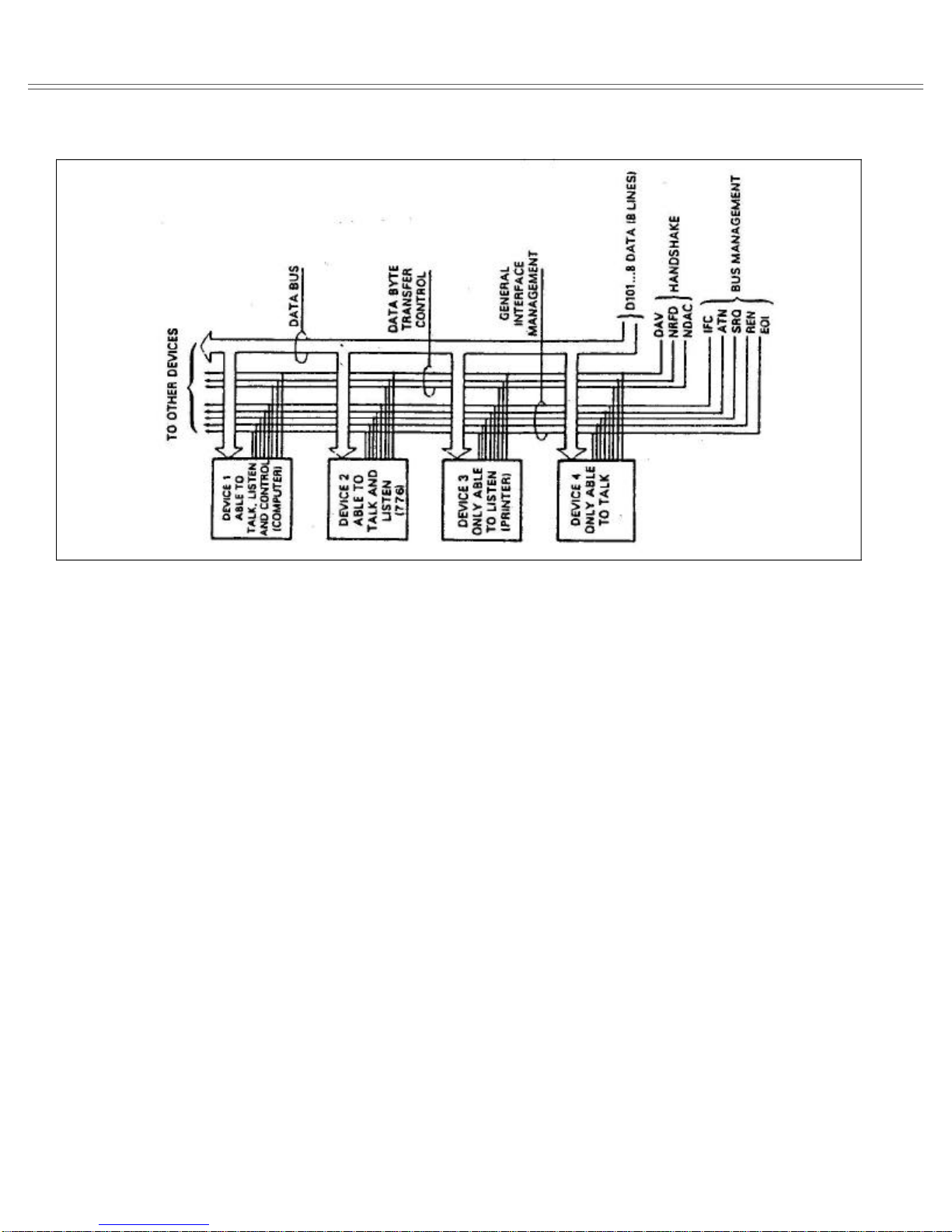
IEEE-488.2 Operation Model 8020
Figure 4-1. IEEE Bus Configuration
Any given system can have only one controller
(control may be passed to an appropriate device
through a special command). Any number of talkers
or listeners may be present up to the hardware
constraints of the bus. The bus is limited to 15
devices, but this number may be reduced if higher
than normal data transfer rates are required or if
long interconnect cables are used.
Several devices may be commanded to listen at
once, but only one device may be a talker at any
given time. Otherwise, communications would be
scrambled much like an individual is trying to select
a single conversation out of a large crowd.
Before a device can talk or listen, it must be
appropriately addressed. Devices are selected on
the basis of their primary address. The addressed
device is sent a talk or listen command derived from
its primary address. Normally, each device on the
bus has a unique primary address so that each may
be addressed individually. The bus also has another
addressing mode called secondary addressing, but
not all devices use this addressing mode.
Once the device is addressed to talk or listen,
appropriate bus transactions may be initiated. For
example, if an instrument is addressed to talk, it will
usually place its data on the bus one byte at a
time. The listening device will then read this information, and the appropriate software is then be used
to channel the information to the desired location.
4-3. IEEE-488 BUS LINES
The signal lines on the IEEE-488 bus are grouped
into three general categories. The data lines handle
bus information, while the handshake and bus management lines assure that proper data transfer and
bus operation takes place. Each of the bus lines is
“active low” so that approximately zero volts is a
logic “one”. The following paragraphs describe the
purpose of these lines, which are shown in Figure
4-1.
4-3-1. Bus Management Lines
The bus management group is made up of five
signal lines that provide orderly transfer of data.
These lines are used to send the uniline commands
described in paragraph 4-8-1.
1. ATN (Attention) - the ATN line is one of the
more important management lines. The state of the
ATN line determines whether controller information
on the data bus is to be considered data or a
multiline command as described in paragraph 4-8-2.
Page 4-2
Page 38
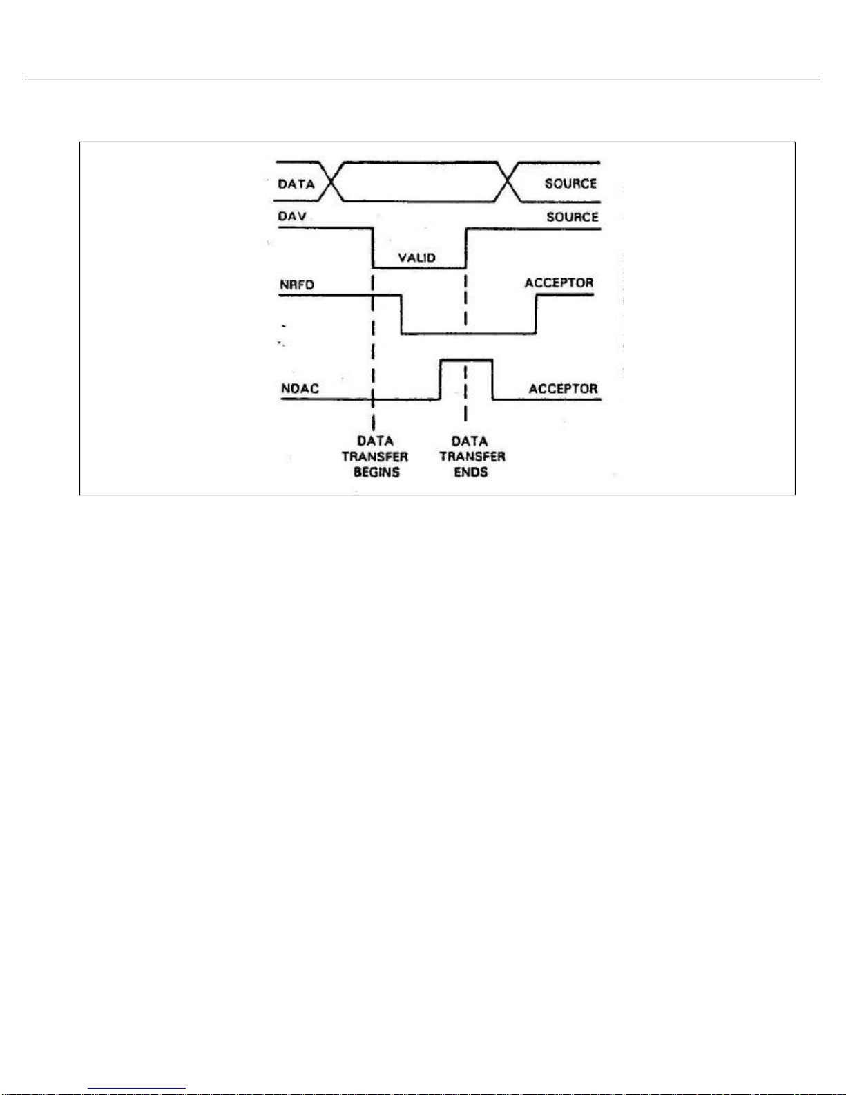
Model 8020 IEEE-488.2 Operation
Figure 4-2. IEEE Handshake Sequence
2. IFC (Interface Clear) - Setting the IFC line
true (low) causes the bus to go to a known state.
3. REN (Remote Enable) - Setting the REM line
low sends the REM command. This sets up instruments on the bus for remote operation.
4. EOI (End Or Identify) - The EOI line is used
to send the EOI command that usually terminates
a multi-byte transfer sequence.
5. SRQ (Service Request) - the SRQ line is set
low by a device when it requires service from the
controller.
4-3-2. Handshake Lines
The bus uses three handshake lines that operate in
an interlocked sequence. This method assures reliable
data transfer regardless of the transfer rate. Generally,
data transfer will occur at a rate determined by the
slowest active device on the bus.
One of the handshake lines is controlled by the
data source, while the remaining two lines are controlled by accepting devices. The three bus handshake
lines are:
1. DAV (Data Valid) - The source controls the
state of the DAV line.
2. NRFD (Not Ready For Data) - the acceptor
controls the state of the NRFD line.
3. NDAC (Not Data Accepted) - the acceptor
also controls the NDAC line.
The complete handshake sequence for one data
byte is shown in Figure 4-2. Once data is on the
bus, the source checks to see that NRFD is high,
indicating that all devices on the bus are ready for
data. At the same time NDAC should be low from
the previous byte transfer. If these conditions are
not met, the source must then wait until the NRFD
and NDAC lines have the correct status. If the
source is controller, NRFD and NDAC must remain
stable for at least 100 ns after ATN is set low.
Because of the possibility of bus hang up, some
controllers have time-out routines to display error
messages if the handshake sequence stops for any
reason.
Once the NRFD and NDAC lines are properly
set, the source sets the DAV line low, indicating
that data on the bus is now valid. the NRFD line
then goes low; the NDAC line goes high once all
devices on the bus have accepted the data. Each
device will release the NDAC line at its own rate,
but the NDAC line will not go high until the slowest
device has accepted the data byte.
After the NDAC line goes high, the source then
sets the DAV line high to indicate that the data on
the bus is no longer valid. At this point, the NDAC
Page 4-3
Page 39

IEEE-488.2 Operation Model 8020
line returns to its low state. Finally, the NRFD line
is released by each of the devices at their own
rates, until the NRFD line finally goes high when
the slowest device is ready, and the bus is set to
repeat the sequence with the next data byte.
The sequence just described is used to transfer
both data and multiline command. The state of the
ATN line determines whether the data bus contains
data or commands.
4-3-3. Data Lines
The IEEE-488.2 bus uses the eight data lines that
allow data to be transmitted and received in a
bit-parallel, byte-serial manner. These eight lines use
the convention DI01 through DI08 instead of the
more common D0 through D7 binary terminology.
The data lines are bi-directional and, as with the
remaining bus signal lines, low is true.
4-4. INTERFACE FUNCTION CODES
The interface function codes are part of the IEEE-
488.2 standards. These codes define an instrument’s
ability to support various interface functions and
should not be confused with programming commands
found elsewhere in this manual.
Table 4-1 lists the codes for the Model 8020.
The numeric value following each one or two letter
code define Model 8020 capability as follows:
SH - (Source Handshake Function) - The ability
for the Model 8020 to initiate the transfer of message/data on the data bus provided by the SH
function.
AH - (Acceptor Handshake Function) - The ability
for the Model 8020 to guarantee proper reception
of message/data on the data bus provided by the
AH function.
T - (Talker Function) - The ability of the Model
8020 to send device-dependent data over the bus
(to another device) is provided by the T function.
Model 8020 talker capabilities exist only after the
instrument has been addressed to talk.
L - (Listen Function) - The ability of the Model
8020 to receive device-dependent data over the bus
(from anther device) is provided by the L function.
Listener function capability of the Model 8020 exist
only after it has been addressed to listen.
RS - (Service Request Function) - The ability of
the Model 8020 to request service from the controller
is provided by the RS function.
Table 4-1. Model 802020 Interface Function Codes
CODE INTERFACE FUNCTION
SH1 Source Handshake Function
AH1 Acceptor Handshake Capabilities
T6 Talker (basic talker, serial
poll, unaddressed to talk on LAG)
L4 Listener (basic listener,
unaddressed to listen on TAG)
SR1 Service request capability
RL1 Remote/Local capability
PP2 Parallel Poll capability
DC1 Device Clear capability
DT1 Device Trigger capability
C0 No controller capability
E1 Open collector bus drivers
TE0 No Extended Talker capabilities
LE0 No Extended Listener capabilities
RL - (Remote-Local Function) - The ability of the
Model 8020 to be placed in remote or local modes
is provided by the RL function.
PP - (parallel Poll Function) - The ability of the
Model 8020 to respond to a parallel poll request
from the controller is provided by the PP function.
DC - (Device Clear Function) - The ability for
the Model 8020 to be cleared (initialized) is provided
by the DC function.
DT - (Device Trigger Function) - The ability of
the Model 8020 to have its output triggered is
provided by the DT function.
C - (controller Function) - The Model 8020 does
not have a controller function.
TE - (Extended Talker Capabilities) - The Model
8020 does not have extended talker capabilities.
LE - (Extended Listener Function) - The Model
8020 does not have extended listener function.
4-5. SOFTWARE CONSIDERATIONS
The most sophisticated computer in the world would
be useless without the necessary software. This
basic requirement is also true of the IEEE-488.2
bus, which requires the use of handler routines as
described in this paragraph. Before a controller can
be used with the IEEE-488.2 interface, the user must
make certain that appropriate handler software is
present within the controller. With the IBM PC computer, for example, the GPIB interface card must be
used with an additional software which contains the
necessary handler software.
Page 4-4
Page 40

Model 8020 IEEE-488.2 Operation
Other small computers that can be used as
controllers have limited IEEE command capability.
The capabilities of some computers depends on the
particular interface being used. Often, little software
“tricks” are required to achieve the desired results.
From the preceding discussion, the message is
clear: make sure the proper software is being used
with the instrument. Often, the user may incorrectly
suspect that a hardware problem is causing fault,
when it was the software that was causing the
problem all along.
4-6. HARDWARE CONSIDERATIONS
Before the instrument can be used with the IEEE-488
bus, it must be connected to the bus with a suitable
connector. Also, the primary address must be properly
programmed as described in this section.
4-6-1. Typical Controlled Systems
The IEEE-488.2 bus is a parallel interface system.
As a result, adding more devices is simply a matter
of using more cables to make the desired connections.
Because of this flexibility, system complexity can
range from simple to extremely complex.
The simplest possible controlled system comprises
a controller and one Model 8020. The controller is
used to send commands to the instrument, which
sends data back to the controller.
The system becomes more complex when additional instruments are added. Depending on programming, all data may be routed through the controller,
or it may be transmitted directly from one instrument
to another.
4-6-2. Connections
The instrument is connected to the bus through an
IEEE-488.2 connector. This connector is designed
to be stacked to allow a number of parallel connections on one instrument.
NOTE
To avoid possible mechanical damage, it is recommended that no more
than three connectors be stacked on
any one instrument. Otherwise, the
resulting strain may cause internal
damage to the connectors.
The IEEE-488.2 bus is limited to
a maximum of 15 devices, including
the controller. Also, the maximum
cable length is 20 meters. Failure to
Table 4-2. IEEE-488 Contact Designations
Contact IEEE-488
Number Designation Type
1 DIO1 Data
2 DIO2 Data
3 DIO3 Data
4 DIO4 Data
5 EOI Management
6 DAV Handshake
7 NRFD Handshake
8 NDAC Handshake
9 IFC Management
10 SRQ Management
11 ATN Management
12 SHIELD Ground
13 DIO5 Data
14 DIO6 Data
15 DIO7 Data
16 DIO8 Data
17 REN Management
18-24 Gnd Ground
observe these limits will probably result in erratic bus operation.
Custom cables may be constructed using the information in Table
4-2. Table 4-2 also lists the contact
assignments for the various bus lines.
Contacts 18 through 24 are return
lines for the indicated signal lines,
and the cable shield is connected to
contact 12. Each ground line is connected to digital common in the Model
8020.
CAUTION
The voltage between IEEE common
and ground must not exceed 0 V or
damage may result to your instrument.
4-7. CHANGING GPIB ADDRESS
The primary address of your instrument may be
programmed to any value between 0 and 30 as
long as the selected address is different from other
devices addresses in the system. This may be
accomplished using a front panel programming sequence. Note that the primary address of the instrument must agree with the address specified in the
controller’s program.
Page 4-5
Page 41

IEEE-488.2 Operation Model 8020
NOTE
The programmed primary address is
briefly displayed during the power-up
cycle of the Model 8020. It is stored
in the non-volatile memory of the
instrument and is retained even when
power is turned off.
To check the present address, or to enter a new
one, proceed as follows:
1. Depress the [2nd] push-button once then depress the [ADR] push-button. The display will be
modified to display the following:
IExx
Where x may be any number from 0 to 30.
2. Use the MODIFIER [x1⇑] or the [x1 ⇓] pushbuttons for selecting a new GPIB primary address.
3. To store the newly selected primary address
depress [EXE]. The instrument then resumes normal
operation.
4-8. BUS COMMANDS
While the hardware aspect of the bus is essential,
the interface would be essentially worthless without
appropriate commands to control the communications
between the various instruments on the bus. This
paragraph briefly describes the purpose of the bus
commands, which are grouped into the following
three categories:
1. Uniline commands: Sent by setting the as-
sociated bus line low (true).
2. Multiline commands: General bus commands
which are sent over the data lines with the ATN
line low (true).
3. Device-dependent commands: Special commands that depend on device configuration; sent
over the data lines with ATN high (false).
4. Common commands and queries: A special
set of commands that all devices must use and
does not depend on device configuration; sent over
the data lines in the same format as the device
dependent commands.
4-8-1. Uniline Commands
Uniline commands are sent by setting the associated
bus line to low. The ATN, IFC, and REN commands
are asserted only by the system controller. The SRQ
command is sent by an external device. The EOI
command may be sent by either the controller or
Table 4-3. IEEE-488 Bus Command Summary
COMMAND TYPE COMMAND STATE OF COMMENTS
ATN LINE(*)
Uniline REN X Set up for remote operation
EOI X Sent by setting EOI low
IFC X Clears Interface
ATN Low Defines data bus contents
SRQ X Controlled by external device
Multiline Universal LLO Low Locks out front panel controls
DCL Low Returns device to default conditions
SPE Low Enable serial polling
SPD Low Disables serial polling Addressed
SDC Low Returns unit to default condition
GTL Low Returns to local control
GET Low Triggers device for reading
Unaddress UNL Low Removes all listeners from bus
UNT Low Removes all talkers from bus
Device- Dependent(**) High Programs Model 802020 for various
modes.
(*) X = Don’t Care, (**) See paragraph 4-9 for complete description
Page 4-6
Page 42

Model 8020 IEEE-488.2 Operation
an external device depending on the direction of
data transfer. The following is descriptions of each
command.
REN - (Remote Enable) - The remote enable
command is sent to the Model 8020 by the controller
to set the instrument up for remote operation. Generally, this should be done before attempting to
program the instrument over the bus. The Model
8020 will indicate that it is in the remote mode by
illuminating its front panel REM indicator. To place
the Model 8020 in the remote mode, the controller
must perform the following steps:
1. Set the REN line true.
2. Address the Model 8020 to listen.
NOTE
Setting REN true without addressing
will not cause the REM indicator to
turn on; however, once REN is true,
the REM light will turn on the next
time an address command is received.
EOI (End Or Identify) - The EOI command is
used to positively identify the last byte in a multi-byte
transfer sequence. This allows variable length data
words to be transmitted easily.
IFC (Interface Clear) - The IFC command is sent
to clear the bus and set hand shake lines to a
known state. Although device configurations differ,
the IFC command usually places instruments in the
talk and listen idle states.
ATN (Attention) - The controller sends ATN while
transmitting addresses or multiline commands. Device-dependent commands are sent with the ATN
line high (false).
SRQ (Service Request) - The SRQ command is
asserted by an external device when it requires
service from the controller. If more than one device
is present, a serial polling sequence, as described
in paragraph 4-8-2, must be used to determine which
has requested service.
4-8-2. Universal Multiline Commands
Universal commands are multiline commands that
require no addressing. All instrumentation equipped
to implement the command will do so simultaneously
when the command is transmitted over the bus. As
with all multiline commands, the universal commands
are sent over the data lines with ATN set low:
LLO (Local Lockout) - The LLO command is sent
by the controller to remove the Model 8020 from
the local operating mode. Once the unit receives
the LLO command, all its front panel controls (except
Power) will be inoperative.
NOTE
The REN bus line must be true before
the instrument will respond to an LLO
command.
To lock out the front panel controls of the Model
8020, the controller must perform the following steps:
1. Set ATN true.
2. Send the LLO command to the instrument.
DCL (Device Clear) - The DCL command may
be used to clear the Model 8020, setting it to a
known state. Note that all devices on the bus
equipped to respond to a DCL will do so simultaneously. When the Model 8020 receives a DCL
command, it will return to the default conditions listed
in Table 4-4. Factory pre-selected parameters are
listed in Table 3-1. To send a DCL command the
controller must perform the following steps:
1. Set ATN true.
2. Place the DCL command on the bus.
SPE (Serial Poll Enable) - The serial polling
sequence is used to obtain the Model 8020 status
byte. Usually, the serial polling sequence is used to
determine which of several devices has requested
service over the SRQ line. However, the serial polling
sequence may be used at any time to obtain the
status byte from the Model 8020. For more information
on status byte format, refer to paragraph 4-14. The
serial polling sequence is conducted as follows:
1. The controller sets the ATN line true.
2. The SPE (Serial Poll Enable) command is
placed on the bus by the controller.
3. The Model 8020 is addressed to talk.
4. The controller sets ATN false.
5. The Model 8020 then places its status byte
on the bus to be read by the controller.
6. The controller then sets the ATN line low and
places SPD (Serial Poll Disable) on the bus to end
the serial polling sequence.
Steps 3 trough 5 may be repeated for other
instruments on the bus by using the correct talk
address for each instrument. ATN must be true when
Page 4-7
Page 43

IEEE-488.2 Operation Model 8020
Table 4-4. Default Conditions. (Status After SDC, DCL, or *RST )
Mode Default Status
Display/Modify D0 Display frequency
Sweep Mode S0 Sweep mode off
Offset Mode O0 Offset mode off
Operating Mode V0 VCO mode off
Gated Mode G0 Gated mode off
Trigger Mode T0 Trigger mode off
Pulse Mode (Model 8021) P0 Pulse mode off
AM Mode (Model 8022) A0 Am mode off
Output Mode (Model 8021) C0 Pulse complement off; Ramp down off
St-by B0 Output stand-by off
Response Message Format X0 Response header OFF
Response Message Terminator Z0 New line(LF), END(EOI) terminator
Event Status Enable Mask *ESE0 No mask
SRQ Enable Register Mask *SRE0 No mask
the talk address is transmitted and false when the
status byte is read.
SPD (Serial Poll Disable) - The SPD command
is sent by the controller to remove all instrumentation
on the bus from the serial poll mode.
4-8-3. Addressed Commands
Addressed commands are multiline commands that
must be preceded by a listen command derived from
the device’s primary address before the instrument
will respond. Only the addressed device will respond
to each of these commands:
SDC (Selective Device Clear) - The SDC command
performs essentially the same function as the DCL
command except that only the addressed device will
respond. This command is useful for clearing only
a selected instrument instead of all devices simultaneously. Model 8020 will return to the default
conditions listed in Tables 3-1 and 4-4 when responding to an SDC command. To transmit the SDC
command, the controller must perform the following
steps:
1. Set ATN true.
2. Address the Model 8020 to listen.
3. Place the SDC command on the data bus.
GTL (Go To Local) - The GTL command is used
to remove the instrument from the remote mode of
operation. Also, front panel control operation will
usually be restored if the LLO command was previously sent. To send the GTL command, the controller
must perform the following sequence:
1. Set ATN true.
2. Address the Model 8020 to listen.
3. Place the GTL command on the bus.
NOTE
The GTL command does not remove
the local lockout state. With the local
lockout condition previously set, the
GTL command will enable front panel
control operation until the next time
a listener address command is received. This places the Model 8020
in the local lockout state again.
GET (Group Execute Trigger) - The GET command
is used to trigger or arm devices to perform a
specific task depends on device configuration. Although GET is considered to be an addressed
command, many devices respond to GET without
being addressed. Using the GET command is only
one of several methods that can be used to initiate
a trigger. More detailed information on triggering can
be found in Section 3 of this manual. To send GET
command over the bus, the controller must perform
the following sequence:
1. Set ATN true.
2. Address the Model 8020 to listen.
3. Place the GET command on the data bus.
GET can also be sent without addressing by omitting
step 2.
Page 4-8
Page 44

Model 8020 IEEE-488.2 Operation
4-8-4. Unaddress Commands
The two unaddress commands are used by the
controller to simultaneously remove all talkers and
listeners from the bus. ATN is low when these
multiline commands are asserted.
UNL (Unlisten) - All listeners are removed from
the bus at once when the UNL commands is placed
on the bus.
UNT (Untalk) - The controller sends the UNT
command to clear the bus of any talkers.
4-8-5. Device-dependent Commands
The meaning of the device-dependent commands is
determined by instrument configuration. Generally,
these commands are sent as one or more ASCII
characters that tell the device to perform a specific
function. For example, M2 is sent to the Model 8020
to place the instrument in the external trigger mode.
The IEEE-488.2 bus treats device-dependent commands as data in providing that ATN is high (false)
when the commands are transmitted.
4-8-6. Common Commands and Queries
Since most instruments and devices in an ATE
system use similar commands which perform identical
functions, the IEEE-488.2 document has specified a
common set of commands and queries which all
device must use. This avoids the problem in which
devices from various manufacturers used a different
set of commands to enable functions and report
status. The IEEE-488.2 treats the common commands
and queries as device dependent commands. For
example, *TRG is sent over the bus to trigger the
instrument. Some common commands and queries,
however, are optional; most of them are mandatory.
The following set of command groups ensure that
all devices communicate uniformly:
1. System Data - These commands are used to
store or retrieve information such as device identification, descriptions and options. It is possible to
determine the manufacturer, model, and serial number
of the device under remote control.
2. Internal Operation - These commands include
such instrument operations as resetting, self-calibrating, and self-diagnostics of a GPIB device. The
device may respond to a calibration query to indicate
that the calibration was carried out successfully and
report any calibration errors that may have occurred.
The reset command sets the device-dependent functions to a known state and must not affect the state
of the IEEE-488 interface, the Service Request Enable
register, or Standard Event Status Enable register.
3. Status and Event - These commands control
the status structure of the GPIB device and provide
a means to read and enable events. Included in
these commands are Clear, Event Status Enable,
Power-on Status, and Service Request Enable.
4. Synchronization - The operation of the devices
within the system are synchronized with these commands. Included is a Wait to Continue command
which forces the devices to complete all previous
commands and queries. The Operation Complete
command tells the device to set bit 0 in the Standard
Event Status register when it completes all pending
operations.
5. Device Trigger - These commands enable a
device to be triggered and specify how it responds
to the trigger message. The Define Device Trigger
command stores a sequence of commands which
the device will follow when the Group Execute Trigger
(GET) is received.
6. Stored Settings - These commands are used
to save the state of the device under control, to be
used at a later time. The Save command stores the
present state of the device in the device’s memory.
If there is more than one location in which this data
can be stored, the command is followed by a number
which designates the storage register to use. The
Recall command restores the state of the device,
as stored in its memory from the previous Save
command. As with the Save command, the Recall
command must be followed by a number to specify
the register from which the stored settings are to
be recalled.
4-9. DEVICE LISTENING FORMATS
This paragraph discusses the formatting of <Program
Message> elements received by a device from its
system interface. Allowable IEEE-488.2 <Program
Message> is composed of sequence of <Program
Message> units, each unit representing a program
command. Each program command is composed of
a sequence of functional syntactic elements. Legal
IEEE-488.2 program commands are created from
functional elements sequences.
Some commands of universal instrument system
application have been defined by the IEEE-488.2.
They are the common commands; these commands
and queries are specific path selections through the
functional syntax diagram as specified in the IEEE-
488.2 standard. The remaining commands are device-specific and are generated by the device designer
Page 4-9
Page 45

IEEE-488.2 Operation Model 8020
using the functional syntax diagram and the needs
of the device. The functional elements include separators, terminators, headers, and data types. These
elements are discussed in the following.
4-9-1. Functional Element Summary
<Program Message> Represents a sequence of
zero or more <Program Message Unit> elements
separated by <Program Message Unit Terminator>
elements.
<Program Message Unit> Represents a single
command or programming data received by the
device.
<Command Message Unit> Represents a single
command or programming data received by the
device.
<Query Message Unit> Represents a single query
sent from the controller to the device.
<Program Data> Represents any of the six different program data types.
<Program Message Unit separator> Separates
the <Program Message Unit> elements from one
another in a <Program Message>.
<Program Data Separator> Separates sequential
<Program data> elements that are related to the
same header.
<Program Header Separator> Separates the
header from any associated <Program Data>.
<Program Message Terminator> Terminates a
<Program Message>.
<Command Program Header> Specifies function
operation. Used with any associated <Program Data
elements>.
<Query Program Header> Similar to <Command
Program Header> except a query indicator (?) shows
that a response is expected from the device.
<Character Program Data> A data type suitable
for sending short mnemonic data, generally where
a numeric data type is not suitable.
<Decimal Numeric Program Data> A data type
suitable for sending decimal integers or decimal
fractions with or without exponents.
<Suffix Program Data> An optional field following
<Decimal Numeric Program Data> used to indicate
associated multipliers and units.
<NonDecimal Numeric Program Data> A data
type suitable for sending integer numeric representation in base 16, 8, or 2. Useful for data that
is more easily interpreted when directly expressed
in a non-decimal format.
<String Program Data> A data type suitable for
sending 7-bit ASCII character strings where the
content needs to be “Hidden” (by delimiters)
<Arbitrary Block Program Data> A data type
suitable for sending blocks of arbitrary 8-bit information.
<Expression Program data> A data type suitable
for sending data that is elevated as one or more
non-expression data elements before further parsing.
4-9-2. Separator Functional Element Summary
The various elements within the <Program Message>
are separated by ASCII characters that were specially
assigned for this purpose. These separators are
discussed in the following paragraphs.
4-9-2-1. Program Message Unit Separator
The <Program Message Unit Separator> separates
sequential <Program Message Unit> elements from
one another within a <Program Message>. The <Program Message Unit Separator> is defined as:
;
It is allowed to use leading <white space> elements
before the <Program Message Separator>. <White
Space> is defined as a single ASCII-encoded byte
in the range of 00-09, 0B-20. This range includes
the ASCII control characters and the space, but
excludes the new line.
4-9-2-2. Program Data Separator
The <Program Data Separator> separates sequential
<Program Data> elements from one another after a
<Command Program Header> or <Query Program
Header>. It is used when a <Command Program
Header> or <Query Program Header> has multiple
parameters. The <Program Data Separator> is defined
as:
,
Preceding and succeeding <White Space> elements
are permitted.
4-9-2-3. Program Header Separator
The <Program Header Separator> separates the
<Command Program Header> or <Query Program
Header> from the <Program Data> elements. The
<Program Header Separator> is defined as white
space:
<White Space>
Refer to paragraph 4-9-2-1 for the definition of <White
Space> elements.
Page 4-10
Page 46

Model 8020 IEEE-488.2 Operation
4-9-3. Program Message Terminator
A <Program Message Terminator> terminates a sequence of one or more definite length <Program
Message Unit> elements. There are three possible
<Program Message Terminator> elements:
1. NL (new line);
2. NL END (EOI); and
3. END (EOI)
NL is defined as a single ASCII-encoded byte
0A (10 decimal). Leading <White Space> elements
are permitted. The instrument interprets any and all
of the three terminators as semantically equivalent.
No alternative encoding are allowed. Note that IEEEP981 amendment forbids the use of CR as a <Program Message Terminator> element. This is because
some controller treat CR as the end of transmission
and leave the LF character in the unit, thereby
creating an error in the controller.
4-9-4. Command Program Header
The <Command Program Header> represents the
operation to be performed in a device. The header
may be optionally followed by associated parameters
encoded as <Program Data> elements. There are
three defined <Command Program Header> elements:
<Simple Command Program Header>, <Compound
Command Program Header>, and <Common Command Program Header.
<Simple Command Program Header> is defined
as:
<Program Mnemonic>
Program Header> causes the device to generate a
response. This element may be optionally followed
by associated parameters encoded as <Program
Data> elements. There are three defined <Query
Program Header> elements: <Simple Query Program
Header>, <Compound Query Program Header>, and
<Common Query Program Header. A <Simple Query
Program Header> is defined as:
<Program Mnemonic>?
For example, FRQ?. Leading <White Space> elements are permitted. Upper/lower case alpha characters are treated with the same semantic equivalence. <Compound Query Program Header> is not
used in model 8020 and will not be discussed here.
A <Common Query Program Header> is defined as:
*<Program Mnemonic>?
For example, *CAL?. Leading <White Space> elements are permitted. Upper/lower case alpha characters are treated with the same semantic equivalence.
4-9-6. Program Data
A <Program Data> functional element is used to
convey a variety of parameter information related to
the <Program Header>.
4-9-6-1. Character Program Data
The <Character Program Data> functional element
is not implemented in Model 8020. Therefore it shall
not be discussed in this manual.
For example, FRQ. Leading <White Space> elements are permitted. Upper/lower case alpha characters are treated with the same semantic equivalence. <Compound Command Program Header> is
not used in model 8020 and will not be discussed
here. A <Common Command Program Header> is
defined as:
*<Program Mnemonic>
For example, *TRG. Leading <White Space> elements are permitted. Upper/ lower case alpha characters are treated with the same semantic equivalence.
4-9-5. Query Program Header
The <Query Program Header> represents the operation to be performed in a device. A <Query
4-9-6-2. Decimal Numeric Program Data
The <Decimal Numeric Program Data> is a flexible
version of the three numeric representations as defined in ANSI X3.42-1975 - NR1, NR2, and NR3.
A <Decimal Numeric Program Data> elements are
defined as:
1. NR1 elements consists of a set of implicit
point representations of numeric values. i.e. (+/)12345.
2. NR2 elements are the representations of explicit
point numeric values. i.e. (+/-)12.345.
3. NR3 elements are representations of scaled
explicit radix point numeric values together with an
exponent notation. i.e. (+/-)123.456E(+/-)3.
Page 4-11
Page 47

IEEE-488.2 Operation Model 8020
4-9-6-3. Suffix Program Data
A <Suffix Program Data> element permits the use
of a suffix following the <Decimal Numeric Program
Data> (NRf). The suffix expression associated units
and (optional) multipliers that modify how the NRf
is interpreted by the device. The presence of a
<Suffix Program Data> after an NRf is always optional.
No particular <Command Program Header> or <Query
Program Header> is a device shall require the use
of a <Suffix Program Data> element.
4-9-6-4. Non-Decimal Numeric Program Data
The <Non-Decimal Program Data> functional element
is not implemented in Model 8020. Therefore it shall
not be discussed in this manual.
4-9-6-5. Arbitrary Block Program Data
The <Arbitrary Block Program Data> functional element is not implemented in Model 8020. Therefore
it shall not be discussed in this manual.
4-9-6-6. Expression Program Data
The <Expression Program Data> functional element
is not implemented in Model 8020. Therefore it shall
not be discussed in this manual.
4-10. DEVICE-DEPENDENT COMMAND
PROGRAMMING
IEEE-488.2 device-dependent commands are sent to
the Model 8020 to control various operating conditions
such as display modify, operating mode, output and
parameter interrogate. Each command is made up
of a program, command or query header followed
by program data, program suffix, and terminated by
program message terminator. The IEEE bus treats
device-dependent commands as data in, providing
that ATN is high when the commands are transmitted.
For example the output amplitude is programmed
by sending the following <Program Message Unit>:
AMP 10.5V.
A number of <Program Message Unit> elements
may be grouped together in one <Program Message>
provided that each <Program Message Unit> is separated by a <Program Message Unit Separator>.
<Program message Unit> elements within a <Program
Message> are executed exactly in the same order
they are received from the controller. The Model
8020 ignores all non-printable ASCII characters (00
HEX through 20 HEX) except the “CR” (carriage
return). A command string is terminated by a <Program Message Terminator> which tells the instrument
to execute the <Program Message>.
If an illegal <Program Header> or <Program Data>
is present within a <Program Message>, the instrument will:
1. Ignore the illegal part or the <Program Mes sage> (but will execute the rest of the <Pro gram Message>).
2. Display an appropriate front panel error mes sage.
3. Set certain bits in its status registers.
4. Generate an SRQ if programmed to do so.
Device-dependent programming aspects are cov-
ered in paragraph 4-8-5 and 4-10.
NOTE
Before programming the instrument
over the bus, It is recommended that
the instrument be set to its default
values by sending an SDC or DCL
over the bus. See paragraph 4-8-3
for information on using the SDC
command.
In order to send a device-dependent or a common
command, the controller must perform the following
sequence:
1. Set ATN true.
2. Address the Model 8020 to listen.
3. Set ATN false.
4. Send the command string over the data bus
one byte at a time.
NOTE
REN must be true when attempting
to program the Model 8020.
Device-dependent commands that affect Models
8020, 8021, and 8022 are listed in Table 4-5.
Common commands and queries are listed in Table
4-6. All the commands listed in the Tables 4-5 and
4-6 are covered in detail in the following.
4-10-1. Display (D)
The display modify command controls what the
Model 8020 places on the display. The eight parameters associated with the display command set
the instrument to display the frequency, amplitude,
Page 4-12
Page 48

Model 8020 IEEE-488.2 Operation
Table 4-5. Device-Dependent Command Summary
Mode Program Header
and Data Description
Display
VFRQ Frequency
VAMP Amplitude
VOFS Offset
VWID Pulse Width (model 8021)
VCAR Carrier Level (model 8022)
VSTP Sweep Stop Frequency
VSWT Sweep Time
VRPT Internal Trigger Period
VMRK Sweep Marker Frequency
VDCO DC Output Level
Sweep Mode
S0 Sweep Off
S1 Log Sweep - Start to Stop (up)
S2 Log Sweep - Stop to Start (down)
S3 Log Sweep - Start to Stop to Start
S4 Log Sweep - Stop to Start to Stop
S5 Lin Sweep - Start to Stop (up)
S6 Lin Sweep - Stop to Start (down)
S7 Lin Sweep - Start to Stop to Start
S8 Lin Sweep - Stop to Start to Stop
Operating Mode
Trigger Mode
Output Mode
V0 VCO Mode Off
V1 VCO Mode On
A0 Amplitude Modulation Off
A1 Amplitude Modulation On
P0 Pulse Width Off
P1 Pulse Width On
O0 Offset Off
O1 Offset On
G0 Gate Mode Off
G1 Gate Mode On
T0 Trigger Mode Off
T1 Trigger Mode On - External Trigger
T2 Trigger Mode On - Internal Trigger
C0 (model 8021) Pulse Complement Off; Ramp Down Off
C1 (model 8021) Pulse Complement On; Ramp Down On
B0 Output Stand-by Off
B1 Output Stand-by On
Page 4-13
Page 49

IEEE-488.2 Operation Model 8020
Table 4-5. Device-Dependent Command Summary (continued)
Mode Header Suffix*
and Data Description Data
Output Waveforms
U0 Sine
U1 Triangle
U2 Squarewave
U3 Fixed base-line positive squarewave
U4 Fixed base-line negative squarewave
U5 DC; Ramp (Model 8021)
Program Parameters
FRQ Program output frequency HZ, KHZ, MHZ
AMP Program output amplitude MV, V
OFS Program output offset MV, V
(Model 8021 only) WID Program pulse width NS, US, MS, S
(Mode 8022 only) CAR Program carrier Level %
STP Program sweep stop HZ, KHZ, MHZ
SWT Program sweep time NS, US, MS, S
RPT Program internal trig. generator per. NS, US, MS, S
MRK Program sweep marker HZ, KHZ, MHZ
(Model 8020 and 8022 only) DCO Program dc output level MV, V
Review Parameters
VFRQ Display output frequency
VAMP Display output amplitude
VOFS Display output offset
(Model 8021 only) VWID Display pulse width
(Mode 8022 only) VCAR Display carrier Level
VSTP Display logarithmic sweep stop
VSWT Display sweep time
VRPT Display internal trig. generator per.
VMRK Display logarithmic sweep marker
(Model 8020 and 8022 only) VDCO Display dc output level
Response Data Query
FRQ? Interrogate output frequency HZ, KHZ, MHZ
AMP? Interrogate output amplitude MV, V
OFS? Interrogate output offset MV, V
(Model 8021 only) WID? Interrogate pulse width NS, US, MS, S
(Mode 8022 only) CAR? Interrogate carrier Level %
STP? Interrogate sweep stop HZ, KHZ, MHZ
SWT? Interrogate sweep time NS, US, MS, S
RPT? Interrogate internal trig. generator per. NS, US, MS, S
MRK? Interrogate sweep marker HZ, KHZ, MHZ
(Model 8020 and 8022 only) DCO? Interrogate dc output level MV, V
STT? Interrogate machine status
* Suffix Data is optional.
Page 4-14
Page 50

Model 8020 IEEE-488.2 Operation
Table 4-5. Device-Dependent Command Summary (continued)
Mode Program Header
and Data Description
Response Message Format
X0 Response header OFF
X1 Response header ON
Z0 New line (LF), END (EOI) terminator
Z1 New line (LF) terminator
Z2 END (EOI) terminator
Z3 No terminator
Common Commands
*CLS Clear status command
*ESE Standard event status enable command
*OPC Operation complete command
*RCL Recall front panel set-up command
*RST Reset command
*SAV Save front panel set-up command
*SRE Service request enable command
*TRG Trigger command
*WAI Wait-to-continue command
Common Queries
*ESE? Standard event status enable query
*ESR? Standard event status register query
*IDN? Identification query
*OPC? Operation complete query
*SRE? Service request enable query
*STB? Read status byte query
*TST? Self-test query
STANDARD EVENT STATUS ENABLE REGISTER MASK
*ESE0 No mask
*ESE1 ESB bit set on operation complete
*ESE2 Not used
*ESE4 ESB bit set on query error
*ESE8 ESB bit set on device dependent error
*ESE16 ESB bit set on execution error
*ESE32 ESB bit set on command error
*ESE64 ESB bit set on user request
*ESE128 ESB bit set on power on
SERVICE REQUEST ENABLE REGISTER MASK
*SRE0 No mask
*SRE1 Not used
*SRE2 RQS/MSS bit set on offset error
(Model 8021 only) *SRE4 RQS/MSS bit set on pulse error
(Model 8021 only) *SRE8 RQS/MSS bit set on ramp error
*SRE16 RQS/MSS bit set on MAV bit
(message available)
*SRE32 RQS/MSS bit set on ESB bit
(standard event status register)
*SRE128 Not used
Page 4-15
Page 51

IEEE-488.2 Operation Model 8020
offset, pulse width (model 8021), carrier level, sweep
stop frequency, sweep time / trigger period or the
sweep marker frequency. The display mode may be
programmed by sending one of the following commands:
VFRQ = Frequency
VAMP = Amplitude
VOFS = Offset
VWID = Pulse Width (model 8021)
VCAR = Carrier Level (model 8022)
VSTP = Sweep Stop Frequency
VSWT = Sweep Time
VMRK = Sweep Marker Frequency
VRPT = Internal Trigger Period
4-10-2. Operating Mode (V, P, A, O)
This command gives the user control over the operating mode of the instrument. The operating mode
may be programmed by sending one of the following
commands:
V0 = VCO Mode Off
V1 = VCO Mode On
P0 = Pulse Mode Off (model 8021)
P1 = Pulse Mode On (model 8021)
A0 = Amplitude Modulation Mode Off (model 8022
only)
A1 = Amplitude Modulation Mode On (model 8022
only)
O0 = Offset Mode Off
O1 = Offset Mode On
4-10-3. Trigger Mode (G, T)
The trigger mode command gives the user control
over the operating mode of the Model 8020. There
are a number of acceptable external sources for
stimulating the function generator. The instrument
may also be set to operate in continuous mode or
with having an internal stimulant. The generator
may be programmed to accept either an external
stimulant or an internal stimulant. Program the Model
8020 to one of the trigger modes by sending one
of the following commands:
G0 = Gated Mode Off
G1 = Gated Mode On
T0 = Triggered Mode Off
T1 = Triggered Mode On - External Trigger
T2 = Triggered Mode On - Internal Trigger
4-10-4. Output Mode (C, B)
The output mode command places the function generator in stand by mode. In model 8021 this command
places the output in pulse complement mode and
in inverted ramp mode. The output mode may be
programmed by sending one of the following commands
C0 = Pulse Complement Off; Ramp Down Off (model
8021)
C1 = Pulse Complement On; Ramp Down On (model
8021)
B0 = Output Stand-By Off
B1 = Output Stand-By On
4-10-5. Waveform (U)
The waveform command give the user control over
the output waveform. The six parameters which are
associated with the waveform commands, set the
instrument to output sinewave, triangle, squarewave,
positive pulse, negative pulse, or DC. The waveform
may be programmed by sending one of the following
commands:
U0 = Sine
U1 = Triangle
U2 = Rectangular
U3 = Positive Pulse
U4 = Negative Pulse
U5 = DC; Ramp Up (model 8021)
4-10-6. Parameter Programming
The parameter programming command sets the function generator to the various levels which are required
for the unit under test. There are 10 different parameters which may be modified using this command.
The command message unit is comprised of three
parts: the <command program header>, the <decimal
numeric program data>, the <suffix program data>
(optional), and the <program message terminator>.
The <command program header> mnemonic is independent of control location on the front panel but
relates to front panel nomenclature. For example,
FRQ mnemonic is related to front panel Frequency
marking.
The <decimal numeric program data> is a flexible
version of numeric representation denoted by NRf.
Operator may choose to program <decimal numeric
program data> using NR1, NR2, or NR3 formats.
Page 4-16
Page 52

Model 8020 IEEE-488.2 Operation
Examples of the various <decimal numeric program
data> is given in the following.
NR1 elements consists of a set of implicit point
representations of numeric values. i.e. (+/-)12345.
NR2 elements are the representations of explicit
point numeric values. i.e. (+/-)12.345.
NR3 elements are representations of scaled explicit
radix point numeric values together with an exponent
notation. i.e. (+/-)123.456E(+/-)3.
The <suffix program data> element permits the
use of suffix following the NRf. The suffix expresses
associated units and (optional) multipliers that modify
how the NRf is interpreted by the device.
For an example, to program the model 8020 for
a frequency output of 10.7 MHz, the following <program message unit> options may be used:
FRQ 10700000; or
FRQ 10.7MHZ; or
FRQ 10.7E+6; or
FRQ 10.7E6HZ; etc.
<Command program header> and <suffix program
data> and (optional) multipliers summary is given in
the following
FRQ ...HZ, KHZ, MHZ = Program frequency
parameter
AMP ...MV, V = Program amplitude parameter
OFS ...MV, V = Program offset parameter
WID ...NS, US, MS, S = Program pulse width
parameter (model 8021 only)
CAR ...% = Program modulated carrier level
parameter (model 8022 only)
STP ...HZ, KHZ, MHZ = Program logarithmic sweep
stop parameter
SWT ...NS, US, MS, S = Program sweep time
parameter
MRK ...HZ, KHZ, MHZ = Program logarithmic
sweep marker parameter
RPT ...NS, US, MS, S = Program internal trigger
generator period parameter
DCO ..MV, V = Program DC output level (models
8020 and 8022 only)
The programming limits for each of the above parameters are listed in Table 3-2. After DCL or SDC,
the instrument defaults to its factory selected values.
Factory defaults are listed in Table 3-1 and 4-4.
4-10-7. Common Commands
As discussed in previous paragraphs most instruments
and devices in an ATE system use similar commands
which perform identical functions to avoids the problem in which devices from various manufacturers
used a different set of commands to enable functions
and report status. Some common commands and
queries, however, are optional; most of them are
mandatory. Common commands and queries are
listed in Table 4-6. The following set of common
commands are utilized in the model 8020 (optional
common commands that are not included in the
model 8020 command set will not be discussed
here).
*CLS (Clear Status Command) - clears status
data structures, and forces the device to the Operation
Complete Command/Query Idle State. If the Clear
Status command immediately follows a <Program
Message Terminator>, the Output Queue and the
MAV bit will be cleared.
*ESE (Standard Event Status Enable Command)
- followed by a number in the range of 0 to 255,
sets the Standard Event Status Enable Register bits.
The binary equivalent of the number represents the
values of the individual bits set into the Standard
Event Status Enable register.
*OPC (Operation complete Command) - causes
the device to generate the operation complete message in the Standard Event Status Register when
all pending selected device operations have been
finished.
*RCL (Recall Command) - restores the state of
the device to a state previously stored in the device’s
memory. If the device has more than one memory
register, the command must be followed by a number
to specify which register is to be used. The functions
restored by the *RCL command are the same as
those affected by the *RST command. Model 8020
may recall settings in registers designated with numbers from 00 to 30.
*RST (Reset) - Sets device-dependent functions
to a known state, purges all *OPC commands and
queries, and aborts all pending operations. The output
queue, Service Request Enable Register, Standard
Event Status Enable Register, and power-on flag
are not affected. Device defaults are listed in Table
4-4
*SAV (Save Command) - allows the user to store
the present state of a device in local memory. If
the device has more than memory location, the
command must be followed by a number to designate
the storage register to be used. Model 8020 may
Page 4-17
Page 53

IEEE-488.2 Operation Model 8020
store settings in registers designated with numbers
from 00 to 30.
*SRE (Service Request Enable Command) - followed by a number, sets the Service Request Enable
register which determines what bit in the status byte
will cause a service request from the device. The
binary equivalent of the number represents the values
of the individual bits of the Service Request Enable
Register.
*TRG (Trigger Command) - has exactly the same
effect as a GET when received, parsed, and executed
by the device.
*WAI (Wait to Continue Command) - causes a
device to wait until all previous commands and
queries are completed before executing any which
follow the *WAI command.
4-10-7-1. Set-ups (*SAV, *RCL)
The setups commands select the memory location
where front panel setup is to be stored (*SAV) or
from where recalled (*RCL). To store or recall a
setup use one of the following commands:
*SAVnn
*RCLnn
Where nn may range from 00 to 30. nn is the
selected memory cell of which the setup is to be
stored or from where the setup is to be recalled.
4-11. DEVICE TALKING FORMATS
This paragraph discusses the formatting of <Response
Message> elements sent from a device via its system
interface. Allowable IEEE-488.2 response message
is composed of a sequence of <Response Message>
units, each unit representing a response to a query.
Each <Response Message> is composed of a sequence of functional syntactic elements. Legal IEEE-
488.2 <Response Message> is created from functional
elements sequences. A <Response Message is interpreted by a controller running an application program, and as such, needs to convey its information
precisely for consistent operation with a wide range
of controllers. A <Response Message>, therefore,
has a more restrictive format than a <Program
Message>.
Some queries of universal instrument system application have been defined by the IEEE-488.2. They
are the common queries; these queries are specific
path selections through the functional syntax diagram
as specified in the IEEE-488.2 standard. The remaining queries are device-specific and are generated
by the device designer using the functional syntax
diagram and the needs of the device. The functional
elements include separators, terminators, headers,
and data types. These elements are discussed in
the following.
Table 4-6. Common Commands and Queries Summary
Mode Program Header Suffix*
and Data Data Description
COMMON COMMANDS *CLS Clear status command
*ESEn Standard event status enable command
*OPC Operation complete command
*RCLn Recall front panel set-up command
*RST Reset command
*SAVn Save front panel set-up command
*SREn Service request enable command
*TRG Trigger command
*WAI Wait-to-continue command
COMMON QUERIES
*ESE? Standard event status enable query
*ESR? Standard event status register query
*IDN? Identification query
*OPC? Operation complete query
*SRE? Service request enable query
*STB? Read status byte query
*TST? Self-test query
Page 4-18
Page 54

Model 8020 IEEE-488.2 Operation
4-11-1. Functional Element Summary
<Response Message> Represents a sequence
of one or more <Response Message Unit> elements
separated by <Response Message Unit Terminator>
elements.
<Response Message Unit> Represents a single
message unit sent from the device.
<Response Data> Represents any of the eleven
different <Response Data> types.
<Response Message Unit Separator> Separates
<Response Message Unit> elements from one another in a <Response Message>.
<Response Data Separator> Separates sequential <Response Data> elements that are related to
the same header or to each other.
<Response Header Separator> Separates the
header from the associated <Response Data>.
<Response Message Terminator> Terminates a
<Response Message>.
<Response Header> Specifies the function of
the associated <Response Data> element(s). Alpha
characters mnemonically indicate the function.
<Character Response Data> A data type suitable
for sending short mnemonic character strings. Generally used when a numeric data type is not suitable.
<Decimal Numeric Response Data> A data type
response suitable for sending decimal integers or
decimal fractions with or without exponents.
<NonDecimal Numeric Response Data> A data
type suitable for sending integer numeric representation in base 16, 8, or 2. Useful for data that
is more easily interpreted when directly expressed
in a non-decimal format.
<String Response Data> A data type suitable
for sending 7-bit ASCII character strings where the
content needs to be “Hidden” (by delimiters). This
element is generally used to send data for direct
display on a device.
<Definite Length Arbitrary Block Response
Data> A data type suitable for sending blocks of
arbitrary 8-bit information when the length is known
beforehand.
<Indefinite Length Arbitrary Block Response
Data> A data type suitable for sending blocks of
arbitrary 8-bit information when the length is not
known beforehand or when computing the length
beforehand is undesirable.
<Arbitrary ASCII Response data> A data type
suitable for sending arbitrary ASCII data bytes when
alternate data types are unworkable.
4-11-2. Separator Functional Element Summary
The various elements within the <Response Message> are separated by ASCII characters that were
specially assigned for this purpose. These separators
are discussed in the following paragraphs.
4-11-2-1. Response Message Unit Separator
The <Response Message Unit Separator> separates
sequential <Response Message Unit> elements from
one another when multiple <Response Message Unit>
elements are sent in a <Response Message>. The
<Response Message Unit Separator> is defined as:
;
4-11-2-2. Response Data Separator
The <Response Data Separator> separates sequential
<Response Data> elements from one another when
multiple data elements are sent. The <Response
Data Separator> is defined as:
,
4-11-2-3. Response Header Separator
The <Response Header Separator> separates the
<Response Header> from the <Response Data>.
The <Response Header Separator> is defined as:
<Space>
4-11-3. Response Message Terminator
The <Response Message Terminator> element’s function is to terminate a sequence of one or more
<Response Message Unit> elements. There are three
possible <Response Message Terminator> elements:
1. NL (new line);
2. NL END (EOI); and
3. END (EOI)
NL is defined as a single ASCII-encoded byte
0A (10 decimal). Leading <White Space> elements
are not permitted. The instrument interprets any and
all of the three terminators as semantically equivalent.
No alternative encoding are allowed. Note that IEEEP981 amendment forbids the use of CR as a <Response Message Terminator> element. This is because some controller treat CR as the end of
transmission and leave the LF character in the unit,
thereby creating an error in the controller.
Page 4-19
Page 55

IEEE-488.2 Operation Model 8020
4-11-4. Response Header
The <Response Header> is available for use by the
device designer for device-specific responses. It may
be used, for example, to create responses in directly
resendable <Program Message Unit> format or to
identify response data to the controller. There are
three defined <Response Header> elements: <Simple
Response Header>, <Compound Response Header>,
and <Common Response Header. A <Simple Response Header> is defined as:
<Response Mnemonic>
For example, FRQ. Leading <White Space> elements are not permitted. Upper/lower case alpha
characters are treated with the same semantic equivalence. <Compound Response Header> is not used
in model 8020 and will not be discussed here. A
<Common Response Header> is defined as:
*<Response Mnemonic>
For example, *SRE. Leading <White Space> elements are not permitted. Upper/ lower case alpha
characters are treated with the same semantic equivalence.
4-11-5. Response Data
1. NR1 elements consists of a set of implicit
point representations of numeric values. i.e. (+/)12345.
2. NR2 elements are the representations of explicit
point numeric values. i.e. (+/-)12.345.
3. NR3 elements are representations of scaled
explicit radix point numeric values together with an
exponent notation. i.e. (+/-)123.456E(+/-)3.
4-12. READING FROM THE MODEL 8020
The reading sequence is used to obtain, from Model
8020, various <Response Message Units> such as
frequency, amplitude, offset or operating modes. The
<Response Message Unit> elements are placed in
an output queue. The output queue may be read
by device-defined queries. Such device-defined queries cause the item read to be removed from the
output queue. Model 8020 executes the <Program
Message> elements in the order received. The output
is cleared when any of the following occur:
1. Reading all the items in the output queue.
2. Upon receipt of a new <Program Message>.
3. Upon receipt of the *CLS, DCL or SDC com-
mands.
4. Upon Power on.
A <Response Data> functional element is used to
convey a variety of response information related to
the <Response Header>. The element type is determined by the eliciting query. <Non-Decimal Response Data>, <String Response Data>, and <Arbitrary Block Response Data> functional elements are
not implemented in Model 8020. Therefore it shall
not be discussed in this manual.
4-11-5-1. Character Response Data
The <Character Response Data> functional element
is used to convey information best expressed
mnemonically as a short alpha or alphanumeric string.
It is useful when numeric parameters are inappropriate, for example, model number and manufacturer
identification.
4-11-5-2. Decimal Numeric Response Data
The <Decimal Numeric Response Data> is a flexible
version of the three numeric representations as defined in ANSI X3.42-1975 - NR1, NR2, and NR3.
A <Decimal Numeric Response Data> elements are
defined as:
IEEE-488.2 specifies that a device cannot send
<Response Message> elements unless commanded
to do so. This is specified as an “Unterminated
Action”. The “Unterminated Action” is executed when
the controller attempts to read a <Response Message> from the device without first having sent a
complete Query Message, including the <Program
Message Terminator>, to the device. In the event
of “Unterminated Action” model 8020 performs the
following steps:
1. Sets the Query Error bit in the Standard Event
Status Register.
2. Clears the output queue.
3. Sets brq False.
If a read sequence is interrupted by a new <Program
Message> before it finishes sending a <Response
Message>, model 8020 executes an “Interrupted
Action”. GPIB bus response is similar to the “Unterminated Action”.
The reading sequence is conducted as follows:
1. The controller sets the ATN line true.
2. The Model 8020 is addressed to talk.
3. The controller sets ATN false.
Page 4-20
Page 56

Model 8020 IEEE-488.2 Operation
4. The instrument sends the information string
over the bus one byte at a time.
5. The controller recognizes that the string is
terminated.
6. The controller sets the ATN line true.
7. The UNT (untalk) command is placed on the
bus by the controller.
4-12-1. Interrogate Parameter Data Query
The interrogate parameter data query allows access
to information concerning present operating conditions
of the instrument. When the interrogate parameter
data query is given, the Model 8020 will transmit
appropriate data string information the next time the
instrument is addressed to talk. Model 8020 Interrogate Parameter Data Query include:
FRQ? = Interrogate output frequency parameter
AMP? = Interrogate output amplitude parameter
OFS? = Interrogate output offset parameter
WID? = Interrogate pulse width parameter
(model 8021 only)
CAR? = Interrogate Carrier level parameter
(model 8022 only)
STP? = Interrogate logarithmic sweep parameter
(model 8020 only)
SWT? = Interrogate sweep time parameter (model
8020 only)
MRK? = Interrogate logarithmic sweep marker pa-
rameter (model 8020 only)
RPT? = Interrogate internal trigger generator
period parameter
DCO? = Interrogate dc output level parame-
ter(model 8020 and 8022 only)
RPT? = Interrogate trigger period parameter
STT? = Interrogate machine status
For example, model 8020 is asked to return
frequency, amplitude, and offset parameters in a
single <Response Message>
Command: FRQ?;AMP?
Response:FRQ 1.000E+3;AMP 1.00E+0
used a different set of commands to enable functions
and report status. Some common commands and
queries, however, are optional; most of them are
mandatory. The following set of common queries are
utilized in the model 8020 (optional common queries
that are not included in the model 8020 command
set will not be discussed here).
*IDN? (Identification Query) - Causes the generator
to respond with its identity. The returned data is
organized into four fields, separated by commas.
The unit must respond with its manufacturer and
model number in the first two fields and may also
report its serial number and options in field three
and four. If the later information is not available, the
device must return an ASCII 0 for each. For example,
model 8021 response to *IDN? is TABOR,8021,0,REV2.0.
*OPC? (Operation Complete Query) - causes the
device to generate the operation complete message
in the Standard Event Status Register when all
pending selected device operations have been finished.
*SRE? (Service Request Enable Query) - enables
the user to read the contents of the Service Request
Enable register. The device returns a number in the
range of 0 to 63 or 128 to 191, since bit 6 (RSQ)
cannot be set. The binary equivalent of the number
represents the value of the bits of the Service
Request Enable Register.
*STB? (Read Status Byte Query) - Reads the
status byte containing the master summary status
(MSS) bit. The device responds with an integer in
the range of 0 to 255, whose binary equivalent
represents the value of the bits of the status byte.
*TST? (Self-Test Query) - Tells the device to
perform an internal self-test and report back to the
controller if any errors are detected. The generator
responds to this query with a number. A value of
1 in the response indicates that the self-test routine
has detected an error. A value of 0 in the response
indicates that the self-test was carried out successfully.
Table 4-7 shows the general <Response Message> format for each of the above commands.
Default values are shown. These defaults are generated after an SDC or DCL commands.
4-12-2. Common Queries
As discussed in previous paragraphs most instruments
and devices in an ATE system use similar commands
which perform identical functions to avoids the problem in which devices from various manufacturers
4-12-3. Response Header (X)
The <Response Header> from the <Response Message> string may be suppressed using this command.
When the <Response Header> is suppressed the
output data string is 3 byte shorter. The <Response
Header> may be suppressed using the following
commands:
X0 = Response header OFF
X1 = Response header ON
Page 4-21
Page 57

IEEE-488.2 Operation Model 8020
4-12-4. Response Message Terminator (Z)
To allow a wide variety of controllers to be used,
the terminator can be changed by sending the appropriate command over the bus. The default value
is New Line (LF), End (EOI) sequence (mode Z0).
The terminator sequence will assume this default
value after receiving a DCL or SDC.
The EOI (END) line on the bus is usually set
low by the device during the last byte of its data
transfer sequence. In this way, the last byte is
properly identified, allowing variable length data words
to be transmitted. The Model 8020 will normally send
EOI during the last byte of its data string or status
word. The <Response Message Terminator> in model
8020 may be programmed by sending one of the
following commands:
Z0 = New Line (LF), END (EOI) terminator
Z1 = New Line (LF) terminator
Z2 = END (EOI) terminator
Z3 = No terminator
NOTES
1. Most controllers use the LF character to terminate
their input sequence. Using the NO TERMINATOR
mode (Z3) may cause the controller to hang up
unless special programming is used.
2. Some controllers may require that EOI be present
at the end of the string.
4-13. DEVICE STATUS REPORTING
Device status reporting defined by IEEE-488.2 builds
upon and extends the original specifications of the
status byte of the IEEE-488.1 document. A complete
model is defined for all status reporting. Figure 4-3
illustrates the IEEE-488.2 status reporting model
showing the IEEE-488.1 status byte, which can be
read by either a serial poll or Status Byte Query.
Summary of related common commands and queries
is given in the following.
*STB? - Returns an NR1, which is the value of
the IEEE-488.1 status byte and the MSS (Muster
Summary Status) summary message.
*OPC - Sets the Operation Complete event bit
in the Standard Event Status Register when all
selected pending device operation have been completed.
*OPC? - Places a “1" in the output queue when
all selected pending operations are completed which
in turn cause the MAV (Message Available) summary
message to be generated.
*CLS - Clears all Event Registers summarized in
the status byte.
*ESR? - Returns an NR1, which is the value of
the Standard Event Status Enable Register.
*SRE NRf - Sets the bits of the Service Request
Enable Register.
*SRE? - Returns an NR1, which is the value of
the Service Request Enable Register.
4-14. STATUS BYTE REGISTER (STB)
The Status Byte Register contains the device’s STB
and RQS (or MSS) messages. IEEE-488.1 defines
the method of reporting the STB and RQS, but
leaves the setting and clearing protocols and semantics for the STB message undefined. The standard
further defines specific device STB summary-messages.
A Muster Summary Status (MSS) message is
also provided which is output as bit 6 with the STB
response to a *STB? common query. The Status
Byte Register is altered only when the state of the
overlaying Status Data Structure is altered. The
description of the various bits within the Status Byte
Register is given in the following.
Bit 0 - Not Used
Bit 1 - Offset Error. The state of this bit indicates
whether or not an offset error occurred. Offset error
may occur when amplitude and offset parameters
exceed the instrument limits and the offset function
is turned on.
Bit 2 - Width Error. The state of this bit indicates
whether or not a pulse width error have occurred.
Width error may occur when the programmed pulse
width is larger than the programmed pulse period
parameter.
Bit 3 - Ramp Error. The state of this bit indicates
whether or not a ramp error have occurred. Ramp
error may occur when ramp parameters exceed the
instrument limits.
Bit 4 - Message Available Queue Summary Message (MAV). The state of this bit indicates whether
or not the output queue is empty. The MAV summary-message is true when the output queue is not
empty. This message is used to synchronize information exchange with the controller. The controller
can, for example, send a query command to the
device and then wait for MAV to become true. If
an application program begins a read operation of
the output queue without first checking for MAV, all
system bus activity is held up until the device
responds.
Page 4-22
Page 58

Model 8020 IEEE-488.2 Operation
Bit 5 - Standard Event Status Bit (ESB) Summary
Message. The ESB summary message is an IEEE-
488.2 defined message. Its state indicates whether
or not one or more of the enabled ESB events have
occurred since the last reading or clearing of the
Standard Event Status Register.
Bit 6 - Master Summary Status (MSS)/Request
Service (RQS) Bit. Its state indicate if the device
has at least one condition to request service. The
MSS bit is not part of the IEEE-488.1 status byte
and will not be sent in response to a serial poll.
The RQS bit, however, if set, will be sent in response
to a serial poll.
Bit 7 - Not used.
4-14-1. Reading the Status Byte Register
The Status Byte Register can be read with either a
serial poll or the *STB? common query. Both of
these methods read the IEEE-488.1 STB message.
The value sent for the bit 6 position is, however,
dependent upon the method used.
4-14-1-1. Reading with a Serial Poll
Table 4-7. Response Message Format Summary
Command Response Format (*)
FRQ? FRQ 1.000E+3(terminator)
AMP? AMP 1.00E+0(terminator)
OFS? OFS 0.00E+0(terminator)
WID? WID 10.00E-3(terminator)
CAR? CAR 100E+0(terminator)
STP? STP 9.000E+3(terminator)
SWT? SWT 1.00E+0(terminator)
MRK? MRK 5.000E+0(terminator)
DCO? DCO 0.00E+0(terminator)
RPT? RPT 1.00E+0(terminator)
(*) NL END is normal terminator. Terminator may change (see paragraph
4-12-4).
binary-weighted values of the Status Byte Register.
The *STB? common query does not alter the status
byte.
4-14-1-3. Clearing the Status Byte Register
When serial polled, the generator returns the 7-bit
status byte plus the single bit RQS message. The
status bye and RQS message are returned to the
controller as a single data byte. The RQS message
is sent on line D107 (bit 6). RQS TRUE means that
bit 6 line is asserted (pulled to a low voltage) when
the status byte is sent. The response represents the
sum of the binary-weighted values of the Status Byte
Register.
Reading the Status Byte Register with a serial
poll sets the RQS message FALSE until a new
reason for service has occurred. The STB portion
of the Status Byte Register is read non-destructively.
The value of the status byte is not altered by a
serial poll. Once the model 8020 has generated an
RQS, its status byte should be read to clear the
SRQ line so the controller can detect an SRQ from
another device. Otherwise the instrument will continuously assert the SRQ line.
4-14-1-2. Reading with the *STB?
The *STB? common query causes the generator to
send the contents of the Status Byte Register and
the MSS (Master Summary Status) summary message
as a single <NR1 Numeric Response Message>
element. The response represents the sum of the
The entire Status Byte Register can be cleared by
removing the reasons for service from the Auxiliary
Status Registers. Sending the *CLS common command to the device after a <Program Message
Terminator> and before <Query Message Unit> elements clears the Standard Event Status Register
and clears the output queue of any unread messages.
With the output queue empty, the MAV summary
message is set to FALSE.
Methods of clearing the other auxiliary status
registers are discussed in the following. The RQS
message in the Status Byte Register will be FALSE.
The use of the IEEE-488.1 DCL or SDC commands
another method of clearing the Status Byte Register,
however, in some cases it is not recommended to
use this method since the entire front panel set-up
is reset to factory default values.
4-14-1-4. Service Request Enable Register
The Service Request Enabling Register is an 8-bit
register that enables corresponding summary messages in the Status Byte Register. Thus, the application programmer can select reasons for the model
8020 to issue a service request by altering the
contents of the Service Request Enable Register.
Page 4-23
Page 59

IEEE-488.2 Operation Model 8020
The Service Request Enable Register is read with
the *SRE? common query. The response to this
query is an number that represents the sum of the
binary-weighted value of the Service Request Enable
Register. The value of the unused bit 6 is always
zero.
The Service Request Enable Register is written
using the *SRE common command followed by a
<Decimal Numeric Program Data> element representing the bit values of the Register. A bit value
one indicates an enabled condition. Consequently, a
bit value of zero indicates a disabled condition. The
Service Request Enable Register is cleared by sending *SRE0. The generator always ignores the value
of bit 6. Summary of *SRE messages is given in
the following.
*SRE0 - No mask.
*SRE1 - Not used.
*SRE2 - Service request on offset error.
*SRE4 - Service request on pulse width error.
*SRE6 - Service request on ramp.
*SRE16 - Service request on MAV.
*SRE32 - Service request on ESB.
*SRE128 - Not used.
4-14-2. Standard Event Status Register (ESR)
Bit 2 - Query Error. This bit indicates that an
attempt is being made to read data from the output
queue when no output is either present or pending.
Bit 3 - Device Dependent Error. This bit is set
when an error in a device function occurs. For
example, the following <Program Message> will cause
DDE error: AMP10E+0;OFS10E+0. Both parameters
are legal and within the specified limits, however,
the function generator is unable to generate such
an amplitude and offset combination. Following the
Device Dependent Error the generator continues to
process the input stream.
Bit 4 - Execution Error. This bit is generated if
the <Program Data> element following the header
is outside of the legal input range of the generator.
Bit 5 - Command Error. This bit indicates the
generator received a command that was a syntax
error, or a command that the device does not
implement. A GET receive inside a <Program Message> will also cause a Command Error.
Bit 6 - User Request. This event bit indicates
that one of a set of local controls, the MANUAL
push-button in this case, has been activated. This
event bit occurs regardless of the remote or local
state of the device.
Bit 7 - Power On. This bit indicates that the
device’s power source was turned off, then on, since
the last time that the register was read.
The Standard Event Status Register is a special
application of the status reporting. IEEE-488.2 document specifies the meaning of each bit of this
register. The 8 bits of the ESR have been defined
by the IEEE-488.2 as specific conditions which can
be monitored and reported back to the user upon
request.
The Standard Event Status Register is destructively read with the *ESR? common query. The
Standard Event Status Register is cleared by a *CLS
common command, on power-on, and when read by
*ESR?.
The arrangement of the various bits within the
register is firm and is required by all GPIB instruments
that implement the IEEE-488.2. Description of the
various bits is given in the following.
Bit 0 - Operation Complete. Generated in response
to the *OPC command. It indicates that the device
has completed all selected and pending operations
and is ready for a new command.
Bit 1 - Request Control. This bit operation is
disabled on model 8020.
4-14-2-1. Standard Event Status Enable
Register (ESE)
The Standard Event Status Enable Register allows
one or more events in the Standard Event Status
Register to be reflected in the ESB summary-message
bit. The Standard Event Status Enable Register is
an 8-bit register that enables corresponding summary
messages in the Standard Event Status Register.
Thus, the application programmer can select reasons
for the model 8020 to issue a ESB summary-message
bit by altering the contents of the ESE Register.
The Standard Event Status Enable Register is
read with the *ESE? common query. The response
to this query is an number that represents the sum
of the binary-weighted value of the Standard Event
Status Enable Register.
The Standard Event Status Enable Register is
written using the *ESE common command followed
by a <Decimal Numeric Program Data> element
representing the bit values of the Register. A bit
value one indicates an enabled condition. Consequently, a bit value of zero indicates a disabled
condition. The Standard Event Status Enable Register
Page 4-24
Page 60
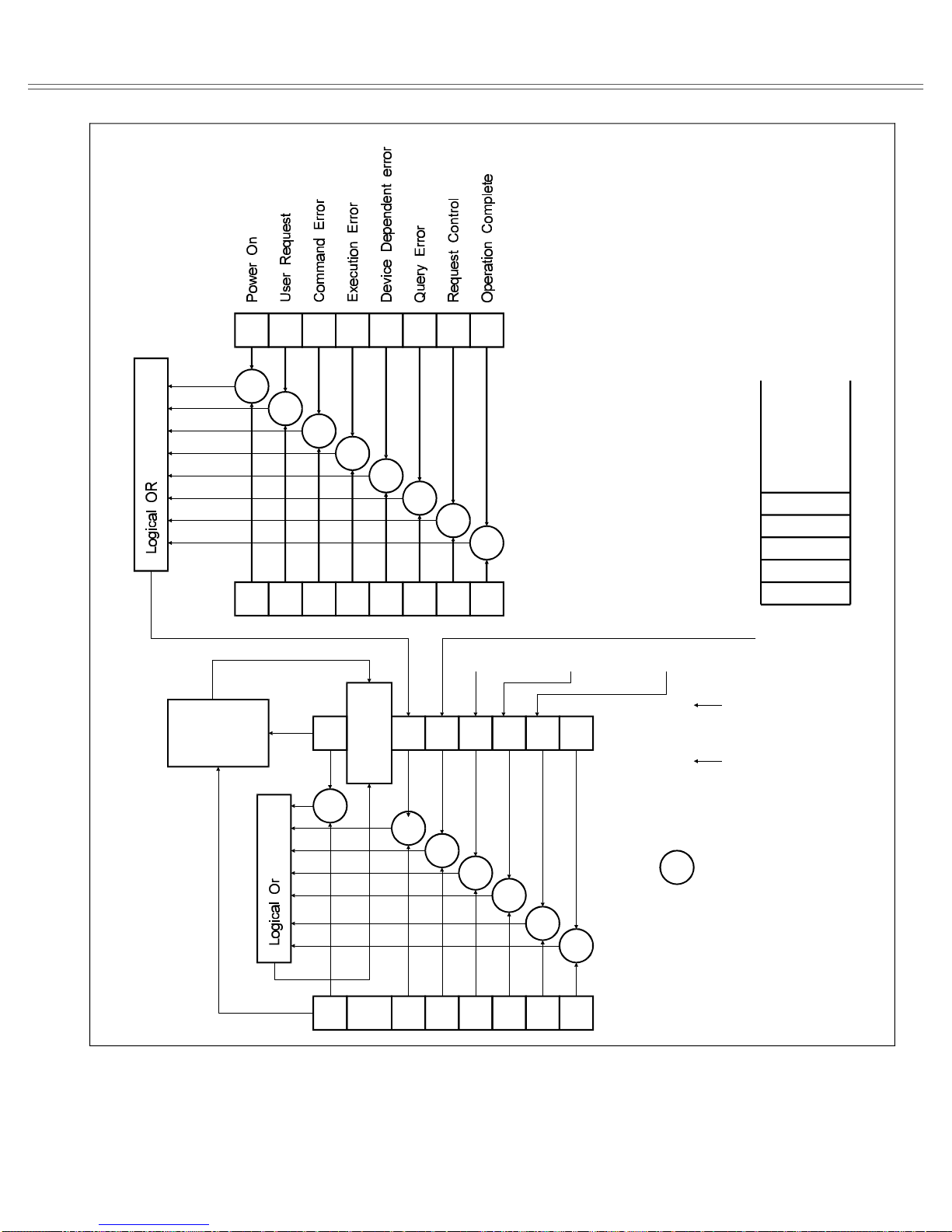
Model 8020 IEEE-488.2 Operation
7 6 5 4 3 2 1 0
7 6 5 4 3 2 1 0
Service
Request
Generation
Standard
Event Status Register
*ESR?
Standard
Event Status Enable
Register
*ESE<NRf>, *ESE?
Output Queue
Ramp Error Pulse Error Offset Error
RQS
7
6
ESB MAV 3 2 1 0
Status Byte Register
MSS
Not Empty
read by Serial Poll
read by *STB?
Figure 4-3. IEEE-488.2 Status Reporting Model
7 5 4 3 2 1 0
= Logical AND
Service Request
Enable Register
6*SRE<NR1>, *SRE?
Page 4-25
Page 61

IEEE-488.2 Operation Model 8020
is cleared by sending *ESE0. Summary of *ESE
messages is given in the following.
*ESE0 - No mask.
*ESE1 - ESB on Operation Complete.
*ESE2 - ESB on Request Control.
*ESE4 - ESB on Query Error.
*ESE6 - ESB on Device Dependent Error.
*ESE16 - ESB on Execution Error.
*ESE32 - ESB on Command Error.
*ESE64 - ESB on User Request.
*ESE128 - ESB Power on.
4-14-3. Machine Status Register (STT)
The Machine Status Register (STT) is a special
register which contain the present front panel setting.
The STT is non-destructively read with the STT?
query. The response to this query is a NR1 <Numeric
Response Data> with the length of 11 digits. These
digits are numeric representation of the various Machine Status options as illustrated in Figure 4-6.
4-15. FRONT PANEL ERROR MESSAGES
The process of programming the Model 8020 involves
the proper use of syntax. Syntax is defined as the
orderly or systematic arrangement of programming
commands or languages. The Model 8020 must
receive valid commands with proper syntax or it will:
1. Ignore the part of the <Program Message Unit>
in which the invalid command appears.
2. Set appropriate bits in the Standard Event Status
Register.
3. Generate an SRQ if programmed to do so.
4. Display an appropriate front panel message.
4-15-1. ILI (Illegal Instruction) Error
An ILI error results when the Model 8020 receives
an invalid <Program Header> such as AMPL1.00.
This command is invalid because the real command
should read AMP1.00. When such an illegal <Program
Header> is detected by the instrument, the following
message will be displayed on the Model 8020 for
about one second:
ILI
4-15-2. ILP (Illegal Parameter) Error
An ILP error occurs when the <Numeric Data>
parameter associated with a legal <Program Header>
command is not valid. For example, the command
AMP100E+0 is not a valid option because the required
amplitude is outside the legal limits of the model
8020. When such an illegal <Numeric Data> is
detected, the following message will be displayed
on the Model 8020 for about one second:
ILP
4-15-3. ILE (Device Dependent) Error
An ILE error occurs when two legal <Program Message> elements and when both elements have legal
<Program data>cause unacceptable conditions for
the instrument. For example, AMP10E+0; OFS6E+0
<Program Message> will cause an ILE error although
each <Program Message Unit> by itself could work
perfactly well under different condition. When such
an error is detected, the following message will be
displayed on the Model 8020 for about one second:
ILE
Figure 4-6. Machine Status String (STT) Interpretation *
<Program Header> D S O V G T P/A C B U X Z
<Progran Data> 0 0 0 0 0 0 0 0 0 0 0 0
* Status given after IEEE-488.1 DCL or SDC commands, or afetr IEEE-488.2 *RST common command.
Page 4-26
Page 62

Model 8020 Maintenance And Performance Tests
SECTION 5
MAINTENANCE AND PERFORMANCE TESTS
5-1. INTRODUCTION
This section provides maintenance, service information,
and performance tests for the 8020 series and for the GPIB
option (option 1). Fuse replacement procedure, line voltage
selection and option installation procedure are also included.
WARNING
The procedures described in this section are
for use only by qualified service personnel.
Do not perform these procedures unless
qualified to do so. Many of the steps covered
in this section may expose the individual to
potentially lethal voltages that could result
in personal injury or death, if normal safety
precautinos are not observed.
5-2. LINE VOLTAGE SELECTION
The Model 8020 may be operated from either 115 V or 230
V nominal 50- 60 Hz power sources. A special transformer
may be installed for 100 V and 200 V ranges. The instrument was shipped from the factory set for an operating
voltage of 230 V. To change the line voltage, proceed as
follows:
5-3. FUSE REPLACEMENT
The Model 8020 has a line fuse to protect the instrument
from excessive current. This fuse may be replaced by
using the procedure described in the following :
WARNING
Disconnect the instrument from the power
line and from other equipment before replacing the fuse.
1. Place the end of a flat-blade screwdriver into the slot in
the LINE FUSE holder on the rear panel. Push in and rotate
the fuse carrier one quarter turn counterclockwise. Release
the pressure on the holder and its internal spring will push
the fuse and the carrier out of the holder.
2. Remove the fuse and replace it with the proper type using
Table 5-1 as a guide.
CAUTION
Do not use a fuse with a rating higher than
specified or instrument damage may occur.
If the instrument persistently blows fuses, a
problem may exist within the instrument. If
so, the problem must be rectified before
continuing operation.
WARNING
Disconnect the Model 8020 from the power
cord and all other sources before changing
the line voltage setting.
1. Using a flat-blade screwdriver, place the line voltage
selection switch in the desired position. The selected voltage is marked on the selection switch.
2. Install a power line fuse consistent with the operating
voltage. See paragraph 5.3.
CAUTION
The correct fuse type must be used to maintain proper instrument protection.
5-4. GPIB INTERFACE OPTION FIELD
INSTALLATION (option 1)
The GPIB (general purpose interface bus) option when
installed permit a connection to an A.T.E bus controllable
system. Detailed information on the IEEE488 standard is
Table 5-1. Line Fuse Selection
POWER LINE VOLTAGE FUSE TYPE
90 - 125V 0.63A, 250V 5x20 mm
195 - 250V 0.315A, 250V, 5x20 mm
Page 5-1
Page 63
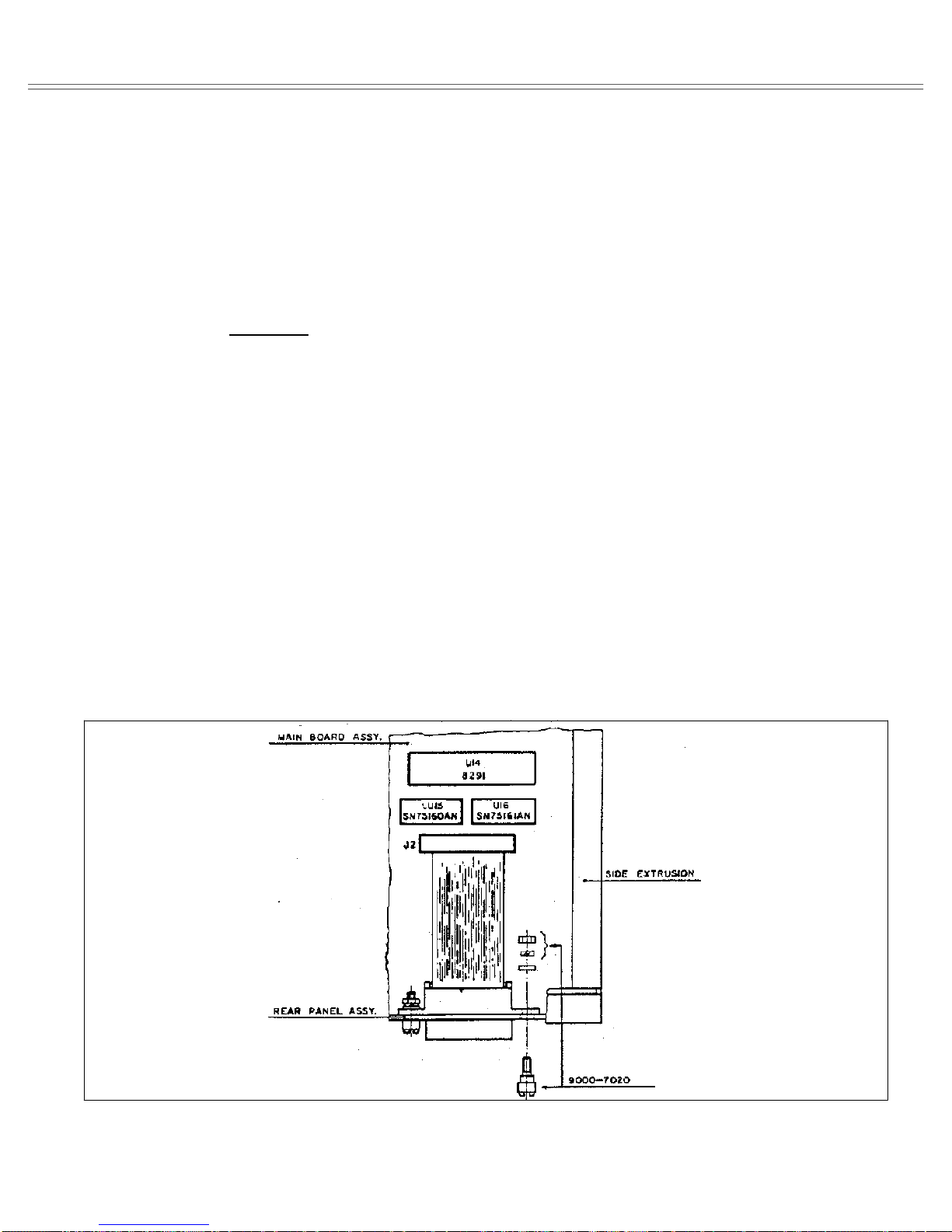
Maintenance And Performance Tests Model 8020
available in Section 4 of this manual. If purchased with the
Model 8020, the option will be factory installed; however
the instrument may easily be upgraded in the field by
installing the option as described in the following procedure.
5-4-1. Option 1 Installation Procedure
1. Remove the top cover of the instrument as described in
the disassembly instructions in paragraph 5-5.
WARNING
Disconnect the line cord and test leads from
the instrument before removing the top
cover.
2. Assemble U47 (8291), U48 (75160) and U49 (75161)
as shown in Figure 5-1.
3. Remove the small plate that covers the rear panel GPIB
opening.
4. Place the GPIB connector onto the rear panel and bolt
the special spacers which are provided with this option, to
the rear panel. It is important to position the GPIB connector exactly in the center of the opening otherwise the
mating connector will not fit. Also only use the special
spacing screws that are supplied with this option. Use
lock-washers to prevent the option from loosening during
transit.
5. Plug the loose end of the flat cable to J2 and press the
connector to secure it to its place. Make sure that the cable
is positioned properly, that pin 1 is connected to pin 1 on
the main board and that no pin on the main board is left
free.
6. Replace the top cover.
7. Turn on the power and observe the power up procedure.
The instrument will display the following as part of its
power-up procedure:
OPt.1
This reading indicates that the instrument accepted the
installed option and is now ready to operate on a bus
controlled system.
5-5. DIASSEMBLY INSTRUCTIONS
If it is necessary to troubleshoot the instrument or replace
a component, use the following disassembly procedure to
remove the top cover:
1. Remove the two screws that secure the top cover to the
rear panel.
2. Grasp the top cover at the rear and carefully lift it off the
instrument. When the tabs at the front of the cover clear
the front panel, the cover may be pulled completely clear.
3. When replacing the top cover, reverse the above procedure; be sure to install the tabs at the front panel before
completely installing the cover.
Figure 5-1. GPIB Interface Option Installation
Page 5-2
Page 64

Model 8020 Maintenance And Performance Tests
5-6. SPECIAL HANDLING OF STATIC SENSITIVE
DEVICES
MOS devices are designed to operate at a very high impedance levels for low power consumption. As a result, any
normnal static charge that builds up on your person or
clothing may be sufficient to destroy these devices if they
are not handled properly. When handling such devices, use
precautions which are described in the following to avoid
damaging them.
1. The MOS ICs should be transported and handled only
in containers specially designed to prevent static build-up.
Typically, these parts will be received in static-protected
containers of plastic or foam. Keep these devices in their
original containers until ready for installation.
2. Remove the devices from the protective containers only
at a properly grounded work station. Also ground yourself
with a suitable wrist strap.
3. Remove the devices only by the body; do not touch the
pins.
4. Any printed circuit board into which the device is to be
inserted must also be grounded to the bench or table. 5.
Use only anti-static type solder sucker.
6. Use only grounded soldering irons.
7. Once the device is installed on the PC board, the device
is normally adequately protected, and normal handling
resume.
5-7. CLEANING
Model 8020 should be cleaned as often as operating condition require. Thoroughly clean the inside and the outside
of the instrument. Remove dust from inaccessible areas
with low pressure compressed air or vacuum cleaner. Use
alcohol applied with a cleaning brush to remove accumulation of dirt or grease from connector contacts and component terminals.
Clean the exterior of the instrument and the front panel
with a mild detergent mixed with water, applying the
solution with a soft, lint-free cloth
Use ordinary 60/40 solder and 35 to 40 watt pencil type
soldering iron on the circuit board. The tip of the iron
should be clean and properly tinned for best heat transfer
to the solder joint. A higher wattage soldering iron may
separate the circuit from the base material. Keep the soldering iron in contact with the PC board for a minimum
time to avoid damage to the components or printed conductors.
To desolder components use a commercial “solder
sipper”, or better, solder removing SOLDER - WICK, size
3. Always replace a component with its exact duplicate as
specified in the parts list.
5-9. PERFORMANCE CHECKS
The following performance checks verify proper operation
of the instrument, and should normally be used:
1. As part of incoming inspection of instrument specifications;
2. As part of troubleshooting procedure;
3. After any repair or adjustment, before returning instru-
ment to regular service.
5-9-1. Environmental Conditions
Tests should be performed under labortory conditions having an ambient temperature of 25 +/-5 deg C and a relative
humidity of less than 80%. If the instrument has been
subjected to conditions outside these ranges, allow at least
one additional hour for the instrument to stabilize before
beginning the adjustment procedure.
5-9-2. Warm-Up Period
Most equipment is subject to at least a small amount of drift
when it is first turned on. To ensure accuracy, turn on the
power to the Model 8020 and allow it to warm-up for at
least 30 minutes before beginning the performance tests
procedure.
5-8. REPAIR AND REPLACEMENT
Repair and replacement of electrical and mechanical parts
must be accomplished with great care and caution. Printed
circuit boards can become warped, cracked or burnt from
exessive heat or mechnical stress. The following repair
techniques are suggested to avoid inadverant destruction
or degradation of parts and assemblies.
5-9-3. Recommended Test Equipment
Recommended test equipment for troubleshooting, calibration and performance checking is listed in table 5-2.
Test instruments other than those listed may be used only
if their specifications equal or exceed the required characteristics.
Page 5-3
Page 65

Maintenance And Performance Tests Model 8020
Table 5-2. Required Test Equipment.
Instrument Recommended Specifications Use (*)
Model
Counter Tabor 6020 200MHz Universal P,A,T
DMM Tabor 4121 .1V- 100V,AC rms,DC P,A,T
Function Generator Tabor 8200 1mHz - 20MHz P
Synthesizer Marconi 2019 80KHz-1040MHz P,A
Oscilloscope Tek 465 100MHz band width P,A,T
Distortion analyser K-H 6900 100Hz - 1MHz P,A
Spectrum analyser HP 182T/8557A 10KHz - 350MHz P
50 ohm feedthrough
Termination Tek 011-0049-01 50 ohm, 2W, 1% P,A
(*) P= Performance Test, A= Adjustments, T= Troubleshooting
5-10. PERFORMANCE CHECKS PROCEDURE
5-10-1. Frequency - Gated Mode
Accuracy specifications: +/-3 % of full scale up to 1.999
MHz; +/-5 % of full scale up to 20.00 MHz
Equipment: Counter
1. Set 8020 as follows:
CONTROL POSITION
Amplitude 1.50 V
Offset 0.00 V
Trigger Mode Continuous
Display Modify FREQ
Operating Mode VCO
Output Squarewave
2. Set counter to frequency measurment.
3. Set 8020 frequency and verify counter frequency reading
as follows:
8020 SETTING COUNTER READING
1.999 Hz 1.940 Hz - 2.060 Hz
19.99 Hz 19.40 Hz - 20.60 Hz
199.9 Hz 194.0 Hz - 206.0 Hz
1.999 KHz 1.940 KHz - 2.060 KHz
19.99 KHz 19.40 KHz - 20.60 KHz
199.9 KHz 194.0 KHz - 206.0 KHz
1.999 MHz 1.940 KHz - 2.060 MHz
20.00 MHz 19.00 MHz - 21.00 MHz
5-10-2. Frequency - Continuous Mode
Accuracy specifications: +/-3 % of full scale up to 9.999 Hz;
+/-0.1 % of full scale up to 20.00 MHz (full scale reading
is 2000 counts)
Equipment: Counter
1. Set 8020 as follows:
CONTROL POSITION
Amplitude 1.50 V
Offset 0.00 V
Trigger Mode Continuous
Display Modify FREQ
Operating Mode Normal
Output Squarewave
2. Set counter to frequency measurment.
3. Set 8020 frequency and verify counter frequency reading
as follows:
8020 SETTING COUNTER READING
19.99 Hz 19.98 Hz - 20.02 Hz
199.9 Hz 199.8 Hz - 200.2 Hz
1.999 KHz 1.998 KHz - 2.002 KHz
19.99 KHz 19.98 KHz - 20.02 KHz
199.9 KHz 199.8 KHz - 200.2 KHz
1.999 MHz 1.998 KHz - 2.002 MHz
20.00 MHz 19.98 MHz - 20.02 MHz
Page 5-4
Page 66

Model 8020 Maintenance And Performance Tests
5-10-3. Amplitude
Accuracy specifications (1KHz): +/-2 % of reading from 1.0
V to 15.0 V; +/-4 % of reading from 10 mV to 1.50 V
Equipment: DMM
1. Set 8020 as follows:
CONTROL POSITION
Frequency 1.000 KHz
Amplitude 15.0 V
Offset 0.00 V
Trigger Mode Continuous
Display Modify AMPL
Operating Mode Normal
Output Squarewave
2. Set DMM to ACV measurments (RMS).
3. Set 8020 amplitude and verify DMM amplitude reading
as follows:
8020 SETTING DMM READING
Square 15.0 V 7.35 V - 7.65 V
Square 1.50 V .720 V - .780 V
Square 150 mV 72.0 mV - 78.0 mV
3. Set 8020 amplitude and verify DMM amplitude reading
as follows:
OFFSET SETTING DMM READING
+/-7.50 V +/-7.40 V to +/-7.60 V
+/-5.00 V +/-4.93 V to +/-5.07 V
+/-750 mV +/-.733 V to +/-.767 V
+/-500 mV +/-.488 V to +/-.512 V
5-10-5. Squarewave Characteristics
Specified transition time: nS (10% to 90% of amplitude)
Specified abberation: 5% of amplitude
Equipment: Oscilloscope
1. Set 8020 as follows:
CONTROL POSITION
Frequency 1.000 MHz
Amplitude 15.0 V
Offset 0.00 V
Trigger Mode Continuous
Display Modify FREQ
Operating Mode Normal
Output Squarewave
Triangle 15.0 V 4.25 V - 4.41 V
Triangle 1.50 V .415 V - .450 V
Triangle 150 mV 41.5 mV - 45.0 mV
Sine 15.0 V 5.22 V - 5.42 V
Sine 1.50 V .511 V - .533 V
Sine 150 mV 51.1 mV - 55.3 mV
5-10-4. DC Characteristics
Accuracy specifications: +/-(1 % of reading + 20 mV) from
-7.50 V to +7.50 V; +/-(2 % of reading + 2 mV) from .750V to +.750V
Equipment: DMM
1. Set 8020 as follows:
CONTROL POSITION
Frequency X (don’t care)
Amplitude X (don’t care)
Function DC
Trigger Mode Continuous
Display Modify AMPL
Operating Mode Normal
2. Set DMM to DCV measurments.
2. Set oscilloscope and verify as follows:
Rise Time 12 nsec Fall Time 12 nsec Overshoot 5% of
amplitude
5-10-6. Sine Charactristics
Specified total harmonic distortion: % from 2 mHz to 19.99
Hz; .5 % from 20 Hz to 100 KHz % from 100 KHz to 1
MHz
Specified harmonic signals: More than 25 dB below the car-
rier level from 1 MHz to 20 MHz
Equipment: Distortion Analyzer, Spectrum Analyser
1. Set 8020 as follows:
CONTROL POSITION
Frequency 10.0Hz
Amplitude 10.0V
Offset 0.00V
Trigger Mode Continuous
Display Modify FREQ
Operating Mode Normal
Output Sine
2. Set Distortion Analyzer to % Distortion measurements
and verify distortion reading as follows:
Page 5-5
Page 67

Maintenance And Performance Tests Model 8020
8020 SETTING DISTORTION ANALYZER
READING
10.00 Hz 1.0 %
100.0 Hz 0.5 %
1.000 KHz 0.5 %
10.00 KHz 0.5 %
100.0 KHz 0.5 %
1.000 MHz 1.0 %
3. Tune Spectrum Analyser for minimum display amplitude and adjust gain so that fundamental corresponds to
0dB.
4. Change 8020 frequency setting to 10 MHz.
5. Verify that all harmonics are less than -25dB
6. Change 8020 frequency setting to 20 MHz.
7. Verify that all harmonics are less than -25dB.
5-10-7. Sine Flatness
Level flatness: .5 dB to 2.000 MHz; .5 dB to 20.00 MHz
Equipment: Oscilloscope
1. Set 8020 as follows:
CONTROL POSITION
Frequency 2.000 KHz
Amplitude 15.0 V
Offset 0.00 V
Trigger Mode Continuous
Display Modify FREQ
Operating Mode Normal
Output Sine
2. Connect 8020 OUTPUT to oscilloscope and set
oscilloscope to display waveform within exactly 6
vertical divisions.
3. Change 8020 Frequency setting to 2.000 MHz. Verify
that peak to peak of displayed waveform is greater than 5.7
divisions.
4. Change 8020 Frequency setting to 20.00 MHz. Verify
that peak to peak of displayed waveform is greater than 5.1
divisions.
5-10-8. Trigger, Gate, Manual
Specifications: Each trigger input cycle or manual button
press generates a gated output signal or a single output
cycle
Equipment: 8200 Function Generator, Oscilloscope
1. Set 8020 as follows:
CONTROL POSITION
Frequency 20.00 KHz
Amplitude 15.0 V
Offset 0.00 V
Trigger Mode Gated
Display Modify FREQ
Operating Mode Nornal
Output Sine
2. Set external 8200 function generator to 1 KHz and 4 V
positive pulse. Connect external 8200 function generator
to TRIG IN BNC. Check on oscilloscope for 8020 output
signal.
3. Disconnect external function generator and press the
MANUAL push- button. Check on oscilloscope for signal
present at 8020 output as long as MANUAL button is
depressed.
4. Change 8020 setting to Triggered mode.
5. Reconnet external function generator to 8020 TRIG IN
terminal.
6. Check on oscilloscope for 8020 output signal. A single
waveshape is generated on every rising edge of the triggering signal.
7. Change 8020 setting to 10Hz.
8. Disconnect external function generator and press the
MANUAL button. check on oscilloscope for a single pulse
after each time the MANUAL button was depressed. Use
TTL output of external function generator to trigger oscilloscope externaly whenever necessary.
5-10-9. Sweep
Specifications: Logarithmic 10 decades, Linear 3 deades,
Automatic up or down, Gated and Triggered sweep
Equipment: Oscilloscope, Counter
1. Set 8020 as follows:
CONTROL POSITION
Frequency 20.00 KHz
Amplitude 15.0 V
Offset 0.00 V
Trigger Mode Continuous
Sweep stop 2.00 KHz
Sweep time 1 Sec
Sweep marker 10.00 KHz
Display Modify TIME
Operating Mode Sweep On
Sweep Type Logarithmic Down
Output Sine
Page 5-6
Page 68

Model 8020 Maintenance And Performance Tests
2. Connect Output terminal to oscilloscope and Set oscilloscope so that sweep may be obseved. Note that 8020
sweeps down.
3. Change 8020 Sweep Time setting throughout the range
and observe that sweep time changes accordingly.
4. Change Sweep type setting to UP and observe that 8020
sweeps up. 5. Connect Sweep Out terminal on the rear
panel to the oscilloscope and observe that DC level changes
2V for a full sweep cycle.
6. Connect Marker out to the oscilloscope and observe that
output changes from 0V to -5V when marker frequency is
reached
7. Change Trigger Mode to Gated
8. Connect an external gating signal to the TRIG IN termi-
nal. Observe that the 8020 sweeps as long as the gating
signal remains high
9. Change 8020 Trigger Mode to Sweep and Triggered and
observe that the 8020 sweeps once for every rising edge of
the triggering signal
NOTE
It is also possible to check the sweep in the
different trigger modes using the MANUAL
button where as long as it is depressed serves
as gating signal in gated mode and as trigger
in triggered mode.
5-10-10. VCO Control
Control amplitude: 0 V to 10 V DC +/-20 %.
VCO control range: 1000:1 change from frequency setting at
2000 counts
Equipment: Power Supply, DMM, Counter
1. Set 8020 as follows:
CONTROL POSITION
Frequency 2.000 MHz
Amplitude 1.50 V
Offset 0.00 V
Trigger Mode Continuous
Display Modify FREQ
Output Squarewave
Operating Mode VCO On
2. Apply power supply output to VCO IN connector and
slowly increase power supply amplitude from 0V to 10 V
+/-20% DC. Verify with counter that output frequency
changes from 2.000 MHz to about 2 KHz.
Performance verification of VCO operation
should be carried out with a very clean DC
voltage. A noisy Power supply output will
cause phase modulation in the 8020 output.
5-10-11. Pulse Width (model 8021)
Accuracy Specifications: +/-(3 % + 4 nSec) from 25 nS to
99.9 mS; +/- 10% from 100 mS to 9.99 S
Equipment: Counter, Oscilloscope, 50 ohm Feed-through
Termination, BNC Cable
1. Set 8021 as follows:
CONTROL POSITION
Amplitude 1.50 V
Offset 0.00 V
Trigger Mode Continuous
Display Modify WID
Operating Mode Pulse
Output Squarewave
2. Set counter to pulse width measurement.
3. Connect 8021 to Channel A of the counter. Set 8021
Pulse Width and Frequency and verify counter reading as
follows:
FREQ WIDTH COUNTER
SETTING SETTING READING
2.000E 6 99.9E-9 100 nS +/-7 nS
500E 3 500E-9 500 nS +/-19 nS
50.0E 3 5.00E-6 5.00 uS +/-.15 uS
5.00E 3 50.0E-6 50.0 uSec +/-1.5 uS
500E 0 500E-6 500 uS +/-15 uS
50.0E 0 5.00E-3 5.00 mS +/-.15 mS
5.00E 0 50.0E-3 50.0 mS +/-1.5 mS
1.00E 0 500E-3 500 mS +/-50 mS
100E-3 5.00E 0 5.00 S +/-500 mS
The following ranges are to be checked using an oscilloscope.
4. Connect 8201 OUTPUT to the oscilloscope input and
verify measurements as follows:
FREQ WIDTH OSCILLOSCOPE
SETTING SETTING READING
10.00 E 6 25.0 E-9 25 nS +/-4 nS
NOTE
Page 5-7
Page 69

Maintenance And Performance Tests Model 8020
5-10-12. Amplitude Modulation (model 8022)
Sensitivity Specifications: 2.5 Vp-p produces 100 % modu-
lation depth when carrier is set to 100 %.
AM Distortion: 1 % at 70 % AM with 1 KHz envelope and 1
MHz carrier.
AM Envelope Bandwidth: DC to 500 KHz.
Equipment: Function generator, Oscilloscope, Distortion
Meter, De- modulator
1. Set 8022 as follows:
CONTROL POSITION
Frequency 1.000 MHz
Amplitude 15.0 V
Offset 0.00 V
Trigger Mode Continuous
Display Modify CARR
Output Sine
Operating Mode AM
2. Connect 8022 output to oscilloscope input. Adjust oscilloscope vertical gain so that trace height is +/-2 vertical
divisions.
3. Set external function generator to output 1 KHz sine
waveform and connect external function generator to AM
IN connector.
4. Adjust amplitude of external generator until oscilloscope
displays 100 % modulation. Remove external generator
from AM input and verify that external generator amplitude is 2.5 Vp-p +/-0.25 V.
5. Change external function generator to 1 KHz sine waveform and 1.2 Vp-p amplitude. Connect external generator
to 8022 AM IN connector.
6. Change external generator frequency setting from 1 KHz
to 500 KHz and 8022 frequency setting to 10.00MHz.
Verify that 8022 output did not decrease by more than 30
%.
7. Change 8022 frequency setting to 1 MHz. Change
external function generator settings to 1 KHz sine waveform and 1.7 Vp-p amplitude. Connect external generator
to 8022 AM IN connector.
8. Connect 8022 output through the AM de-modulator to
the distortion analyzer. Verify that distortion is less than 1
%.
Page 5-8
Page 70

Model 8020 Theory Of Operation
SECTION 6
THEORY OF OPERATION
6-1. INTRODUCTION
This section contains an overall functional description of
the 8020 series function generators as well as detailed circuit analysis of the various sections of the instruments. Information pertaining to the pulse width, the amplitude
modulation and the standard IEEE interface (Option 1) are
also included.
Information is arranged to provide a description of individual functional circuit blocks. As an aid to understanding, the descriptions are keyed to accompanying
block diagrams and simplified schematics. Detailed schematics and component layout drawings are located at the
end of this instruction manual.
6-2. OVERALL FUNCTIONAL DESCRIPTION
The 8020 series is a line of fully programmable function
generators having various standard output functions. All
parameters are adjustable through front panel touch
switches or through IEEE programming. The high performance of the 8020 series is accomplished by utilizing a
very fast, discrete analog circuits. Microprocessor and
digital circuits control the performance of the analog circuits and permit direct interfacing to the front panel keyboard and display and to the optional IEEE-488 GPIB; option 1.
A simplified block diagram of the instrument is shown
in Figure 6-1. The heart of the function generator is its
VCO, where two identical currents with opposite polarities are created. These two currents are switched in, on and
off, charging and consequently discharging a capacitor.
This cycle generates a continuous reclining and declining
voltage ramps. The repetition rate depends on the applied
capacitor and the supplied current.
attenuated through the output amplifier and fed to the
OUTPUT connector. The output amplifier is capable of
driving its waveforms into a 50 load.
External gating or triggering effect the current which
is supplied to the current generator.
The analog signals are controlled by D to A converters.
The D to A converters receive their controlling information through serial to parallel converters; directed by the
microprocessor components.
6-3. ANALOG CIRCUITRY
The following paragraphs contain descriptions of the current generator the VCO (voltage controlled oscillator) the
sine shaper the trigger circuit the final amplifier and the
attenuators. Complete and detailed schematics are located at the end of this manual.
6-3-1. Current Generator
The current generator generates the necessary currents for
the VCO and the trigger circuits. Figure 6-2 is a simplified
diagram of the current generator. The current generator is
composed of the following sections: Reference source,
DAC, Up/Down current sources, and trigger current
source. Each one is discussed in detail below.
REFERENCE SOURCE - The reference source generates the voltage for the DAC. The reference comprises a
zener diode CR13, operational amplifier U33 and their associated components. When used as a voltage controlled
oscillator, an external voltage is applied to the VCO input
terminal through U48 and U49. This voltage is then fed
through U33 to the current generator.
The same ramp is used for driving the triangle and the
squarewave buffers. The triangle waveform is also utilized in generating the sinewave output by using a sine
shaper. The three basic waveforms are then amplified or
DAC - The DAC (digital to analog converter) includes
U34 and operational amplifier U28. Shift registers U29
and U30 control the digital information for the data inputs
Page 6-1
Page 71
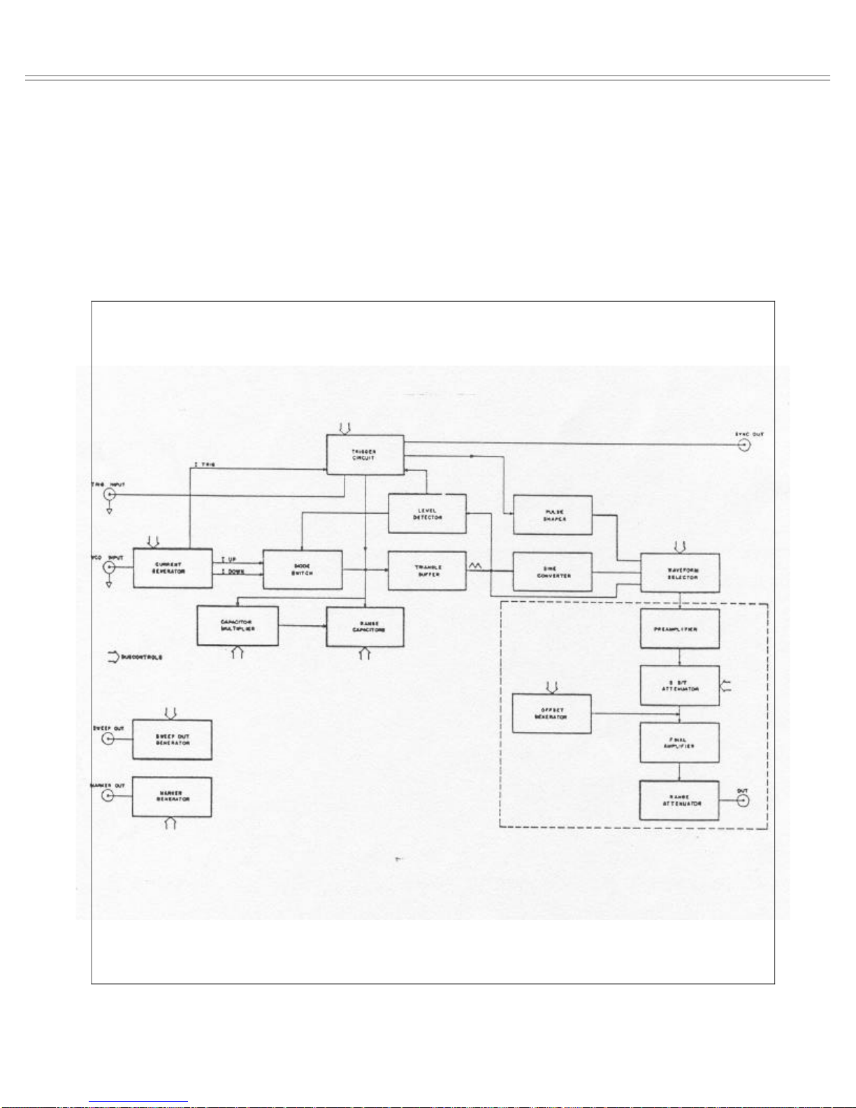
Theory Of Operation Model 8020
of U34. The reference for the DAC is provided from the
output of the reference source.
UP/DOWN CURRENT SOURCES - The output from
the DAC from U34 is voltage shifted by Q10 and applied
to a voltage mirror U27 and Q9. The emitter of Q9 drives
the up current source while the collector, through CR8
drives the down current source. The up current source is
Figure 6-1. Model 8020 - Symplified Block Diagram
formed by U25, Q6 and their associated components. The
down current source is formed by U26, Q7 and their associated components.
TRIGGER CURRENT SOURCE - The same precisioncurrent generator, which supplies the down current
source, supplies the current to the trigger current source.
The trigger current source is doubled and compared with
Page 6-2
Page 72
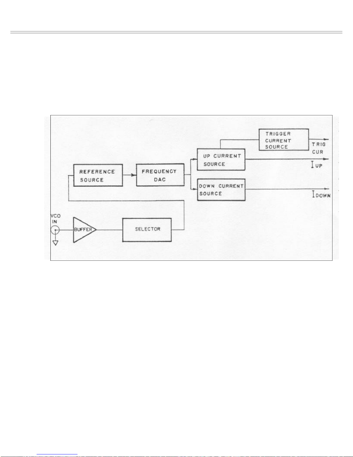
Model 8020 Theory Of Operation
the down current source. The trigger current source is
comprised of the Q8 and R19.
6-3-2. Voltage Controlled Oscillator
Figure 6-3 is a simplified block diagram of the VCO sec-
Figure 6-2. Current Generator Simplified Block Diagram
the feedthrough from the switch drive signal to the range
capacitors.
TRIANGLE BUFFER - The triangle buffer includes impedance converter FET Q19, transistors Q22, 23, 24 and
Q25 and their associated components.
tion. Refer to this Figure throughout the following descriptions. Assuming that the diode bridge switch is operating in such a way that I up is flowing to the range capacitor, the capacitor is charged with this current which creates
a positive going voltage ramp. This voltage ramp is fed
through an impedance converter to the triangle buffer.
This buffer isolates the capacitors from the level detector
and provides sufficient voltage amplitude for the level detector. When the voltage ramp reaches a predetermined
threshold level, the level detector operates the diode
switch so that the current now flows through the I down
source. This causes the same reaction as described above
but with opposite direction. The following paragraphs describe the voltage controlled oscillator in depth.
DIODE SWITCH - The diode switch consists on the following parts: CR19, CR20, CR17, CR18, CR21 and
CR22. The up current is supplied through R67 and the
down current is supplied through R68. CR17 and CR19 as
well as CR18 and CR20 are connected in series to reduce
LEVEL DETECTOR - The level detector consists of
U43 and Q27 through Q30. The positive threshold is set by
R101 and R107 and the negative threshold is set by R104
and R106. The rectangular signals which are then used to
switch the diode switch are taken from Q27 and Q30. Q26
with CR23, CR24 and CR25 translate the rectangular
waveform from the collector of Q28 to a TTL level signal
which is then sent to the trigger circuitry.
RANGE CAPACITORS - The frequency at the main output is being generated by charging capacitors which also
create the triangle waveform. The range capacitors C38
through C46 are used for the 20Hz to 20MHz ranges. U38
receives the serial data from the digital circuit, converts
the serial data to parallel information which is fed to the
quad comparator U39. The outputs of the quad comparator are then fed to the bases Q15 through Q18 which in turn
select the correct range capacitor.
Page 6-3
Page 73
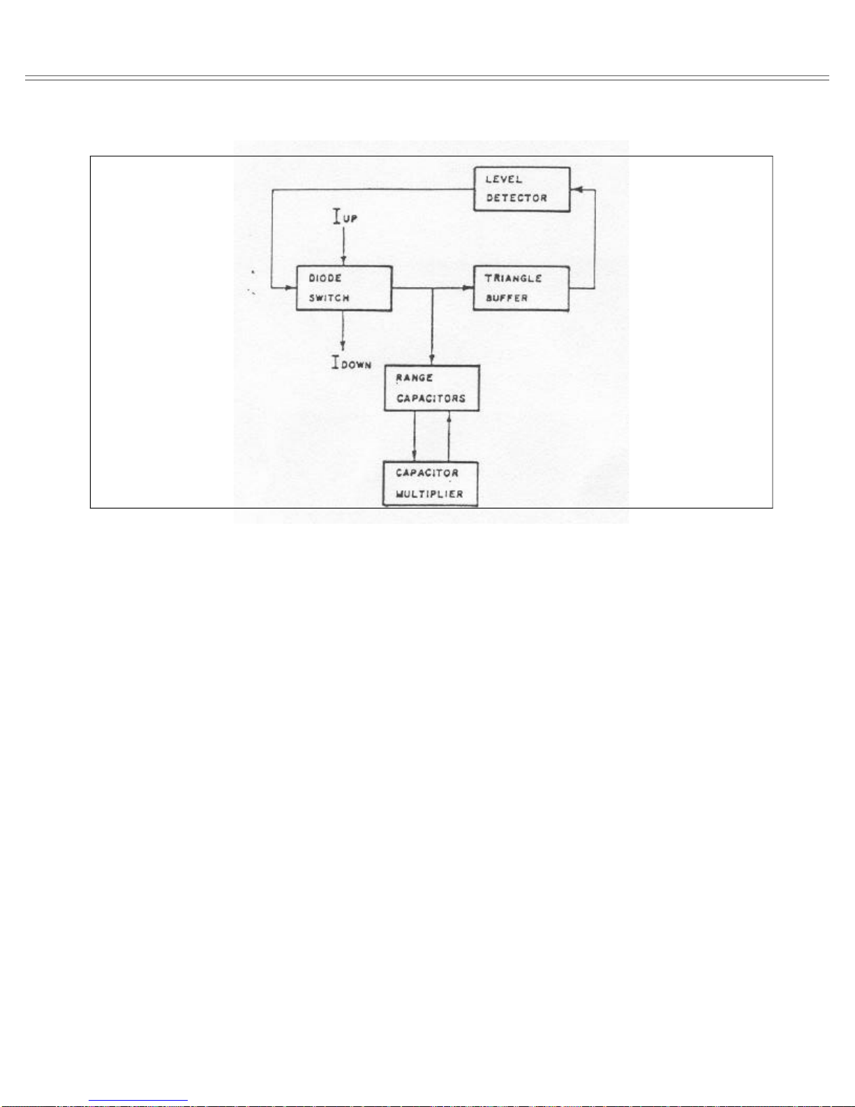
Theory Of Operation Model 8020
Figure 6-3. VCO Simplified Block Diagram.
CAPACITOR MULTIPLIER
plier is used for the 2mHz to 19.9Hz ranges. The function
of this circuit is to generate an equivalent large capacitance. The larger values of capacitors are required to generate lower frequencies. The capacitor multiplier is
formed by U40 ,U41 and their associated components.
The multiplier ratio is selected by changing the ranging
resistors in the negative feedback path of U40. The ranging resistors are selected by Q43 and analog switch U42.
The switching control is provided by the serial to parallel
converter U38.
6-3-3. Sine Shaper
The sine shaper consists of a series of differential stages
which are formed by the transistor arrays U45, U46 and
U47. The differential stages are connected in parallel and
receive the drive signal from the triangle buffer output.
This circuit takes advantage of the non- linear characteristics of the transistors and by biasing them to different
dc levels, the output of the common collector is shaped to
a sinewave. The sinewave is then amplified and re-biased
to oscillate around 0V with a differential amplifier which
is formed by Q34, Q35, Q36 and Q37, U45b, U45c and
their associated components.
- The capacitor multi-
6-3-4. Trigger Circuit
The trigger circuit is active when one of the trigger modes
is selected. The trigger circuit is composed of two main
sections: the clamp circuit and the trigger logic circuit.
Figure 6-4 is a simplified block diagram of the clamp circuit. Refer to this Figure and to the schematic diagrams at
the end of this manual throughout the following description. Detailed description of the clamp and the trigger
logic circuits is provided in the following. Description is
given for both trigger and gated modes.
CLAMP CIRCUIT
U24, Q20, Q21 and their associated components. When
no trigger mode is selected, U24 is cleared with its inverted
Q output set to “1". At this time, the trigger current flows
through Q20. Q21, which is connected as a diode, is reversed biased and do not interfere with normal VCO operation.
Selecting one of trigger or gated modes its inverted Q
output is modified to “0". The up current from the VCO
circuit is diverted through Q21 to the junction of Q20 and
Q21. Due to the fact that the Current from the trigger current is double that of the up or down currents, the current
flow through Q20 will equal to that flowing through Q21.
Under these conditions, the clamp level, at the triangle
buffer input will be set to logical ”0" level. This sequence
- The clamp circuit is composed of
Page 6-4
Page 74
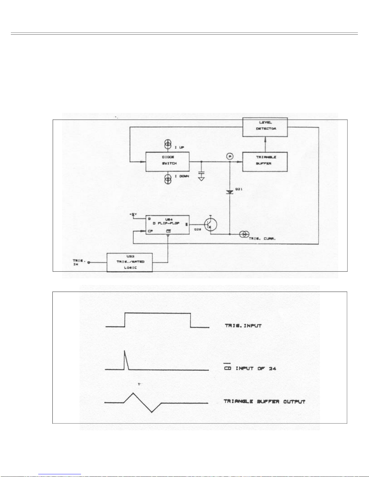
Model 8020 Theory Of Operation
clamps the input of the triangle buffer to a level which is set
by the clamp voltage generator.
Figure 6-5 shows the waveforms of the clamp circuit in
triggered operating mode and Figure 6-6 shows the waveforms of the clamp circuit in gated operating mode.
Figure 6-4. Model 8020 Clamp Circuit Simplified Diagram
TRIGGER LOGIC - The trigger logic is formed by U22
and U24. The triggering signal is routed through R12 to the
input of U22A. Selecting continuous mode sets the control inputs of U22b and U22c to “0". This sets U24 to ”0"
level and keeps Q21 off. This action blocks any signals
coming from the trigger input.
Figure 6-5. Model 8020 Clamp Circuit Waveforms (Triggered Mode)
Page 6-5
Page 75
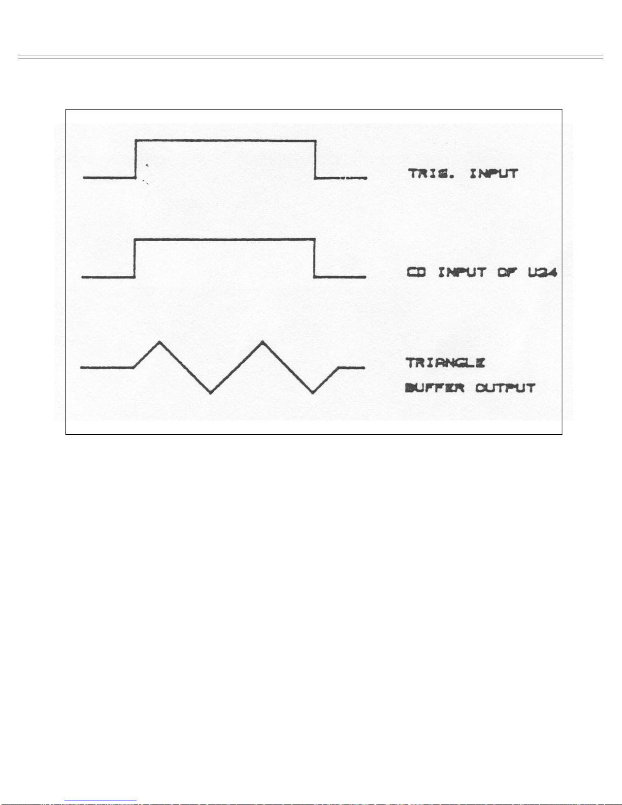
Theory Of Operation Model 8020
Figure 6-6. Model 8020 Clamp Circuit Waveforms (Gated Mode)
When the generator is set to operate in Gated mode the
gating signal is routed through U22 to U24. The VCO is
enabled when the gating signal is high and disabled when
the gating signal is low.
Selecting triggered mode, sets the controlling input to
U22B to high and the controlling input to U22C to low. A
positive transition from the trigger input generates a narrow negative going pulse at U24. This sequence in turn
enables one cycle at the VCO output.
6-3-5. Pulse Shaper
The purpose of the pulse shaper is to convert the signal
from the level detector to pulses having very fast rise and
fall times and with precise amplitude. The pulse shaper is
located on the output amplifier assembly board. Refer to
the schematics at the end of this manual throughout the
following description.
The pulse from the VCO is routed via U1 to the pulse
shaper. The pulse shaper consists of Q1, Q2, Q3 and Q4,
Page 6-6
positive current generator Q10 and negative current generator Q9. When the generator is set to operate in squarewave function, the output of the pulse shaper, alternates
between the positive current source and the negative current source. When in positive pulse function, the output
alternates between the positive current source and ground
and when in negative pulse function, the output alternates
between the negative current source and ground. The
positive current source consists of U3, Q10 and their associated components. R127 adjusts the positive current. Q7
controls Q8 when positive pulse is selected. The negative
Current source consists of U2, Q9 and their associated
components. R126 adjusts the negative current amplitude. Q5 controls Q6 when negative pulse is selected.
6-3-6. Preamplifier
The pre-amplifier is located on the output amplifier assembly board. Refer to the schematics at the end of this
manual throughout the following description. The preamplifier consists of U11, Q12, Q13, Q14, Q15 and Q16 and
their associated components. U8 is a serial to parallel con-
Page 76

Model 8020 Theory Of Operation
verter which operates the quad comparator U9 which in
turn operates signal selector U10. U10 selects one of the
following signals: triangle, sinewave or pulses from the
pulse shaper. The signal from the selector is fed in parallel
to a low frequency amplifier U11 and its associated components and through C17 and C18 to the high frequency
amplifier. The output of the preamplifier, at the junction
of R46 and R47 is then routed to the attenuator. Q12 is a 10 dB gain switch which connects R54 in parallel to the
feedback resistor R56.
6-3-7. Attenuator
The attenuator is located on the output amplifier assembly
board. Refer to the schematics at the end of this manual
throughout the following description. The attenuator is
controlled by 3 quad comparators U5, U6 and U7. The data
which is required to operate the comparators is converted
from serial to parallel by U4. The attenuator is connected
in a binary fashion and comprises FETs Q17 through Q32.
One or more switches are on at a time which in turn changes
the equivalent resistance from the preamplifier to the
power amplifier. This adjusts the amplitude level to the
correct level for the output power amplifier.
6-3-8. Offset Generator
The offset generator is located on the output amplifier assembly board. Refer to the schematics at the end of this
manual throughout the following description. The offset
generator generates a DC voltage which is summed with
the selected waveform. The DC voltage is generated by
the D/A converter U14 and operational amplifiers U15
and U16. The reference voltage level is generated by
CR21 and is adjusted by R99. The D to A converter is controlled by serial to parallel converter U13. U17 is connected as a comparator which, when commanded from
U19, turns FET switch Q35 on or off; changing the polarity
of the DC offset. The DC offset amplitude is coupled
through R79 to the output power amplifier.
6-3-9. Power Amplifier
Refer to the schematics at the end of this manual throughout the following description. The output amplifier consists of low frequency amplifier U18, high frequency amplifier Q33, Q34 and Q39 through Q46 and class B power
stage Q38 through Q43. The signal is coupled to the low
frequency amplifier through R95 and to the high frequency amplifier through C36 and C42. The output from
the power amplifier at the junction of R117 and R118 is
connected through a 50 ohm resistance to the decade attenuator.
6-3-10. Post Amplifier Attenuator
The post amplifier attenuator is the final stage through
which the signal is fed. Attenuation ranges from 0dB to
30dB. U19 receives serial information from the microprocessor serial bus, converts the serial information to parallel and operates relays K1, K2 and K3 through buffer
U20. The relays select one of the divider networks which
are formed by the resistors R120 through R125. Relay K3
disconnects the output signal from the output terminal
when a disable command is given through the IEEE bus.
6-3-11. Power Supply
Refer to the power supply schematic at the end of this manual for the following discussions. The power supply consists of a main power transformer, three bridge rectifiers,
four regulators and a 5V regulator which is formed by U21,
Q3, Q4 and Q5, and their associated components. The
LINE fuse and the Line Selector are accessible at the rear
panel. The LINE VOLTAGE SELECT switch select
115V or 230V operation. CR2 is used as a full-wave rectifier to provide a sufficient DC voltage for the -24V and
+24V regulators U17 and U18 respectively. CR1 is used
as a full-wave rectifier to provide a sufficient DC voltage
for the -15V and +15V regulators U19 and U20 respectively. U21 receives a reference voltage of 5V from the
15V supply. This reference is compared with the 5V supply. The difference is amplified by U21 and Q5 and applied
to the series regulator Q3 which, in turn, corrects the output voltage to equal that of the reference voltage.
6-4. PULSE GENERATOR CIRCUIT (model 8021)
The pulse generator circuit is constructed on the same
board as the output amplifier. The complete assembly,
which includes the above sections plus the pulse generator
circuit, is unique to the model 8021. In the following, only
the section pertaining to the pulse generator is described.
The rest of the circuits are identical to those available on
the model 8020. Figure 6-8 is a functional block diagram.
For complete and detailed schematics, refer to the back of
this manual.
In general, the heart of the pulse generator circuit is the
switching transistor. This transistor when turned off or on
enables a charge or discharge sequence respectively on the
range capacitor. The charge current and the selected capacitor determine the width of the pulse.
Page 6-7
Page 77
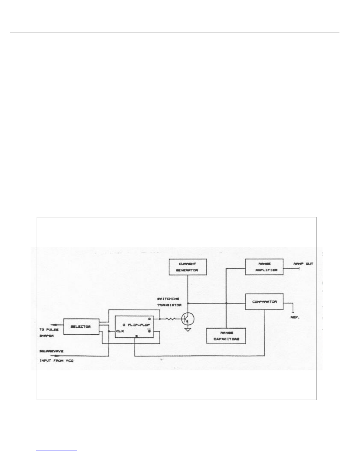
Theory Of Operation Model 8020
The sequence is initiated from a steady state condition
where the switching transistor is on. At that time the current generator, the range capacitor and the comparator input are shorted to ground. The output from the comparator
is set to “1". A positive transition from the VCO circuit
modifies the state of the flip-flop turning the transistor off.
The current from the current generator is allowed to flow
to the range capacitor. The capacitor is charged to a level
equal to the reference voltage. At that time the comparator
flips its output state to ”0", forcing this sequence to an end.
The following describes the various sections of the pulse
generator in details.
CURRENT GENERATOR - The current generator is
composed of D/A converter U36, Serial to parallel converter U37 and voltage reference CR41. The CPU generates serial data which is converted to parallel information
by U37. CR41 generates a precise voltage which controls
the accuracy of the current generator. The current generator is made of an operational amplifiers U33 and U35, and
transistors Q67 through Q70. The current is supplied to
the selected capacitor through the collector of Q67.
RANGE CAPACITORS - Serial data from the CPU is
converted to parallel information by U30 and U38. The
parallel information, through switching transistors Q62,
Q64, Q65, Q60, Q61 Q75 and Q76, is then used for selecting the appropriate capacitor from one of C79 through C86
and C106 respectively.
COMPARATOR - The comparator circuit consists of a
FET buffer Q66, a monolithic comparator U34 and their
associated components. The reference voltage is generated from the +15V supply by the resistor divider R193 and
R196.
SELECTOR - The selector circuit U31 selects one of the
pulse, pulse complement or square waveforms. One of
these waveforms are then fed to the pulse shaper.
RAMP AMPLIFIER - The ramp amplifier is comprised
of operational amplifiers U39 and U40. U41 controls FET
switches Q73 and Q74. These switches select ramp polarity.
Figure 6-7. Pulse Generator Functional Block Diagram.
Page 6-8
Page 78
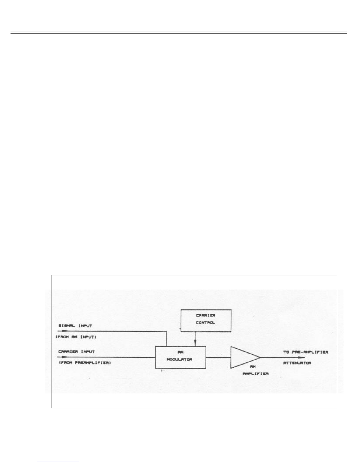
Model 8020 Theory Of Operation
6-6. DIGITAL CIRCUITRY
6-5. AM CIRCUIT (model 8022)
Model 8020 operation is supervised by the internal microThe AM circuit is constructed on the same board as the
output amplifier. The complete assembly, which includes
the above sections plus the AM circuit, is unique to the
model 8022. In the following, only the section pertaining
to the amplitude modulation circuit is described. The rest
of the circuits are identical to those available on the model
8020. Figure 6-9 is a functional block diagram. For complete and detailed schematics, refer to the back of this manual.
processor (CPU). The CPU controls parameter selection
process, front panel switching, the displayed read-out and
IEEE operation. All of these tasks are performed under
software supervision. This section briefly describes the
operation of the various sections of the microprocessor
and its associated digital circuitry. A simplified block dia-
gram is included for user reference. For more complete
circuit details refer to the digital schematics at the end of
this manual.
The modulator is composed of transistor arrays U24
and U25, transistors Q47, Q48 and Q56 and their associated components. The carrier is applied to the base of Q47.
The modulating signal is applied through R130, U25,
R131 and R174 to the modulator circuit. Carrier level is
controlled by U21. U21 receives serial data from the CPU
and converts this data to parallel information for driving
U22.
AM AMPLIFIER - The AM amplifier is a differential
amplifier consisting of transistors Q49 through Q54 and
their associated components. The output, at the junction of
R163 and R167 is fed through a relay K4 to the pre-amplifier circuit.
Figure 6-8. AM Circuit Functional Block Diagram.
Circuit operation centers around the microprocessor
unit (CPU) U5. The CPU is an 8-bit microprocessor capable of directly addressing up to 64K bytes of program
memory (ROM) and up to another 64K bytes of data memory (RAM). The microprocessor works with a 10 Mhz
clock which is divided by U6 to provide clocks for the various sections of the instrument. Software for the CPU is
contained in one EPROM U8 containing 32K bytes of
memory space. Temporary storage is provided by RAM
U9 which can store up to 2K bytes of information.
6-6-1. Display And Keyboard Interface
Interfacing between the CPU, the keyboard and the display is performed by the Keyboard/Display interface U2.
The information for the seven segment LEDs is sent
through buffer U1 and limiting resistors RN1. U1 multiplex the digits and LED and drive the high current transis-
Page 6-9
Page 79

Theory Of Operation Model 8020
tors Q1 through Q8 which, in turn, drive the anodes of the
appropriate LED. The sense lines S0, S1 and S2 determine
which of the button were depressed.
6-6-2. Counter Circuit
The counter circuit is employed in the model 8020 for the
purpose of controlling the accuracy of the frequency at the
output connector. The counter circuit is composed of divider U10, selector U11, D flip-flop U12 and selector U13.
The counter circuit counts the number of pulses from the
VCO. The CPU then computes the relation between these
pulses to the reference clock. The result is compared to the
required accuracy. If deviation is sensed, the CPU sends
correcting data to the current generator circuit.
6-6-3. IEEE-488 Interface (option 1)
The instrument has a built in IEEE-488 interface that permits remote control through a system controller.
The IEEE interface is made up of U11, (General Purpose Interface Adapter), U15 and U16 interface bus drivers. On the CPU side of the GPIB, data transmission is handled much like any other bus transaction. The output of the
U14 is standard IEEE format and is buffered by the two
IEEE bus drivers U15 and U16. The bus divers are necessary for enhancing the drive capability of the interface. Up
to 15 devices may be connected in parallel.
Page 6-10
Page 80

Model 8020 Adjustments
SECTION 7
ADJUSTMENTS
7-1. INTRODUCTION
This section contains information necessary to adjust the
8020 series, the pulse generator circuit (model 8021) and the
amplitude modulation circuit (model 8022).
WARNING
The procedures described in this section are
for use only by qualified service personnel.
Do not perform these procedures unless qualified to do so. Many of the steps covered in this
section may expose the individual to potentially lethal voltages that could result in personal injury or death if normal safety precautions are not observed.
7-2. ADJUSTMENTS
7-2-1. Environmental Conditions
Adjustments should be performed under laboratory conditions having an ambient temperature of 24 +/-5 degC and a
relative humidity of less than 70 %. If the instrument has been
subjected to conditions outside these ranges, allow at least
one additional hour for the instrument to stabilize before beginning the adjustment procedure.
7-2-2. Warm-Up Period
7-2-4. Adjustment Procedures
All adjustments are performed with the POWER switch ON.
The top cover should be removed to allow access to test points
and adjustments. Between adjustments, always leave top
cover on the unit to keep internal temperature.
WARNING
Take special care to prevent contact with live
circuits or power line area which could cause
electrical shock resulting in serious injury or
death. Use an isolated tool when making adjustments. Use plastic or nylon screw-driver
when adjusting the time base trimmer as other
material will cause confusion in this adjustment.
Refer to the component layout in Section 9 when necessary for determining adjustment points. Follow the procedure in the sequence indicated because some of the adjustments are interrelated and dependent on the proceeding
steps.
Verify that Model 8020 is functioning according to the
performance checks. Make sure that all results are within, or
close to, the range of the required specifications, otherwise
refer to the troubleshooting procedures given later in this section.
Most equipment is subject to at least a small amount of drift
when it is first turned on. To ensure long-term calibration
accuracy, turn on the power to the Model 8020 and allow it to
warm-up for at least 20 minutes before beginning the adjustment procedure.
7-2-3. Recommended Test Equipment
Recommended test equipment for calibration is listed in Table 5-3. Test instruments other than those listed may be used
only if their specifications equal or exceed the required characteristics.
Center all trimmers and if necessary, remove selected
components and clear the holes to allow a selection of new
components.
Perform the following adjustment procedure. If an adjustment can not be made to obtain a specific result, refer to
the troubleshooting procedures.
NOTE
If not otherwise specified, set Model 8020
controls as follows and terminate the OUTPUT with a 50 ohms feedthrough termination.
Page 7-1
Page 81

Adjustments Model 8020
CONTROL POSITION
Frequency As required by procedure
Amplitude 1.00 V
Offset 0.00 V
Sweep Stop 2.0 MHz
Sweep Time 1 S
Sweep Marker 10 MHz
Operating Mode Normal (all lights off)
Trigger Mode Continuous (all lights off)
Output Squarewave
7-3. ADJUSTMENT PROCEDURE
7-3-1. Power Supply Adjustment
Equipment: DMM
1. Set DMM to DC measurements. Measure and record the
-15 V supply voltage with 10 mV resolution.
2. Adjust R4 so that the +15 V supply would be the same as
the voltage level recorded in step 1.
7-3-2. Distortion Adjustment
Equipment: Distortion Analyzer, Oscilloscope
1. Change 8020 Output setting to Sine.
2. Change 8020 Frequency setting to 2.000 KHz.
3. Set the oscilloscope to 1V/Div. and DC coupling and adjust
the trace line vertically to be exactly at the center of the screen
(0 V).
4. Connect the OUTPUT terminal to the oscilloscope and adjust R172 to get a symmetrical waveform, about the 0V line,
on the screen.
5. Disconnect the OUTPUT from the oscilloscope and connect the OUTPUT to the distortion analyzer.
6. Adjust R115 and R129, repeatedly, until the distortion
reading on the analyzer is less than 0.2%. Note that each one
of these resistors contribute a small amount to the distortion
correction. It is up to the service technician to find the most
effective sequence to perform this step.
7. Disconnect the OUTPUT from the analyzer and repeat
steps 3 and 4.
input. Terminate counter input with 50 ohms feedthrough
termination.
4. Set counter to frequency measurements and adjust R29 for
a reading of 1.990 KHz +/-10 Hz on the counter display.
5. Change 8020 Frequency setting to 19.90 KHz and check
that the reading on the counter is 19.90 KHz +/-30 Hz. If read ing is not within the specified value readjust R29 so that the
error in 1.990 KHz and 19.90 KHz is the same.
6. Change 8020 Frequency setting to 2.00 MHz.
7. Set counter and adjust C38 to give a reading of 2.00 MHz
+/-30 KHz on the counter display.
8. Set the oscilloscope to 20 mV/Div. and DC coupling and
adjust the vertical trace line to be exactly at the center of the
screen (0 V). Connect a 10:1 high frequency probe,with a
very short ground lead, to the junction to TP7. Adjust the vertical gain of the oscilloscope so that the peak to peak amplitude on the screen will be exactly 6 divisions. Change 8020
frequency setting to 15.00 MHz. Select C56 and adjust C60
until peak to peak trace is 6 divisions +/-1 small division.
Note that the trace should be vertically symmetrical about the
0 V line.
9. Readjust C60 to give a reading of 15.00 MHz +/-300 KHz
on the counter display.
10. Change 8020 Frequency setting to 2.00 MHz.
11. Check with counter if reading is 2.00 MHz +/-30 KHz. If
reading is not within the specified value readjust C38.
12. Repeat steps 9 through 11 until best accuracy is achieved.
13. Change 8020 Frequency setting to 199.0 KHz.
14. Set counter and select C44 (approximately 330PF) to give
a reading of 199.0 KHz +/-3 KHz on the counter display.
15. change 8020 Frequency setting to 1.990 MHz.
16. Select C41 (approximately 47PF) to give a reading of 1.990
MHz +/-30 KHz on the counter display.
7-3-4. Low Frequency Adjustment
Equipment: Counter
1. Change 8020 Frequency setting to 10.00 Hz.
2. Connect the 8020 OUTPUT terminal to the counter.
3. Adjust R59 to 10.00 Hz +/-.1 Hz.
7-3-3. Frequency Adjustment
Equipment: Counter, Oscilloscope, 50 ohms feedthrough
termination
1. Change 8020 operating mode setting to VCO.
2. Change 8020 Frequency setting to 1.990 KHz.
3. Connect the OUTPUT terminal to the universal counter
Page 7-2
7-3-5. Low Frequency Distortion Adjustment
Equipment: Distortion analyzer, Counter
1. Change 8020 Frequency setting to 10.00 Hz.
2. Change 8020 Output setting to sine.
3. Connect 8020 OUTPUT terminal to the distortion analyzer
input.
4. Adjust R44 for minimum distortion.
Page 82

Model 8020 Adjustments
5. Disconnect the 8020 OUTPUT from the distortion analyzer and reconnect it to the counter input.
6. Change 8020 Output setting to squarewave.
7. Verify that the frequency reading on the counter is 10.00
Hz +/-.1 Hz. If reading is not within range, repeat steps 7-3-4
and 7-3-5 until all adjustments are within the specified range.
7-3-6. Trigger Start Phase Adjustment
Equipment: DMM
1. Change 8020 front panel settings as follows:
Output setting to Triangle.
Trigger setting to Gated.
Amplitude setting to 15.0 V.
2. Connect DMM to 8022 output connector.
3. Set DMM and select R73 for a DMM reading of 0 V +/-.1
V.
7-3-7. Amplitude Adjustment
Equipment: DMM (RMS)
1. Change 8020 Amplitude setting to 15.0 V.
2. Change 8020 Frequency setting to 1.000 KHz.
3. Set DMM to ACV measurements and connect 8020 OUT-
PUT through a 50 ohms feedthrough termination to the
DMM.
4. Set Output waveform and perform adjustments, on the amplifier board assembly, as in the following table:
4. Adjust R99, on the amplifier board assembly to give a reading of 7.00 V +/-50 mV on the DMM.
5. Change 8020 offset setting to -7.00 V.
6. Verify that DMM reading is -7.00 mV +/-50 mV. If not
within range re- adjust R99 to compromise between the two
readings.
7-3-9. Squarewave Response Adjustment
Equipment: Oscilloscope, 50 ohms feedthrough termination
1. Temporarily install C23 - 6.8 pF and C21 - 15 pF.
2. Change 8020 Frequency setting to 1.000 MHz.
3. Change 8020 Amplitude setting to 15.0 V.
4. Connect 8020 OUTPUT connector, through a 50 ohms
feedthrough termination, to the oscilloscope input.
5. Set oscilloscope to 20 uS/Div. and adjust the Vertical control on the oscilloscope to display the square waveform in
exactly 6 vertical divisions.
6. Change oscilloscope setting to 5 nS/Div.
7. Adjust C62, on the amplifier board assembly for the best
rise/fall times and for minimum overshoot and undershot. If
necessary, select C23 for best pulse response.
8. Change 8020 Amplitude setting to 1.50 V and verify that
the response is within the limits. If necessary, re-select C21
for best pulse response.
7-3-10. Sine Flatness Adjustments
Equipment: Oscilloscope, 50 ohms feedthrough termination
OUTPUT ADJUST- RERQUIRE
WAVEFORM MENT DMM READING
Sine R39 5.31V +/-20mV
Triangle R38 4.33V +/-20mV
Positive Pulse R127 3.75V +/-10mV
Negative Pulse R126 3.75V +/-10mV
Square —- 7.50V +/-20mV
7-3-8. Offset Adjustment
Equipment: DMM, 50 ohms feedthrough termination
1. Change 8020 frequency setting to 1.000 KHz and amplitude setting to 1.00 V.
2. Change 8020 Offset setting to 7.00 V and turn offset on.
3. Set DMM to DCV measurements and connect 8020 OUT-
PUT, through a 50 ohms feedthrough termination to the
DMM.
1. Change 8020 Function setting to Sine.
2. Change 8020 Frequency setting to 100.0 KHz.
3. Change 8020 Amplitude setting to 15.0 V.
4. Connect 8020 OUTPUT, through a 50 ohms feedthrough
termination, to the oscilloscope.
5. Adjust oscilloscope controls to display the Sinewave with
exactly 6 vertical divisions peak to peak.
6. Change 8020 Frequency setting to 20 MHz.
7. Select C6 (approximately 10 pF), on the amplifier board
assembly, so that the sinewave amplitude on the screen will
be within the range of 5.1 to 5.3 vertical divisions.
Page 7-3
Page 83

Adjustments Model 8020
7-3-11. Triangle Flatness Adjustments
Equipment: Oscilloscope, 50 ohms feedthrough termination
1. Change 8020 Function setting to Triangle.
2. Change 8020 Frequency setting to 100.0 KHz.
3. Change 8020 Amplitude setting to 15.0 V.
4. Connect 8020 OUTPUT, through a 50 ohms feedthrough
termination, to the oscilloscope.
5. Adjust oscilloscope controls to display the triangle with
exactly 6 vertical divisions peak to peak.
6. Change 8020 Frequency setting to 20 MHz.
7. Select C7 (approximately 15PF), on the amplifier board
assembly, so that the triangle amplitude on the screen will be
within the range of 5.1 to 5.3 vertical divisions.
7-3-12. Reference Oscillator Adjustment
Equipment: Counter
1. Set counter for frequency measurements. Using a :10
probe, measure the frequency at pin 3 of U14.
2. Select C68, on the main board assembly, for a counter reading of 5.0000 MHz +/- 100 Hz.
7-3-13. Pulse Width Adjustment (model 8021 only)
Equipment: Counter
1. Connect 8021 output through a 50 ohms feedthrough termination to the counter input. Set counter and 8021 settings
and adjust controls on the final amplifier board assembly, as
follows:
8021 WID 8021 FREQ COUNTER
SETTING SETTING ADJUST READING
5.00 mS 100.0 Hz R211 5.00 mS +/-50 uS
500 uS 1.000 KHz R211* 500 uS +/-5 uS
50.0 uS 10.00 KHz C84 50.0 uS +/-.5 uS
500 nS 1.000 MHz C89 500 nS +/-10 nS
25.0 nS 1.000 MHz R188 25.0 nS +/-2 nS
(Repeat last two steps)
5.00 uS 100.0 KHz C86 5.00 uS +/-50 nS
* Repeat adjustments until best accuracy is achieved.
7-3-14. Ramp Amplitude Adjustment (model 8021 only)
Equipment: Oscilloscope
1. Set 8021 output to ramp, frequency setting to 1.000 KHz,
pulse width setting to 500 uS and amplitude setting to 6.0 V.
2. Set oscilloscope input to DC coupling and vertical gain to
be 1 V/div. Adjust trace vertical position so that it appears 3
divisions below the center line.
3. Connect 8021 output, through a 50 ohms feedthrough termination, to oscilloscope input. Select R218 so that the base
line is set to three divisions below the center line.
4. Adjust R213 for a peak to peak amplitude of 6 vertical divisions.
7-3-15. Amplitude Modulation Adjustment (model 8022
only)
Equipment: Oscilloscope, function generator, DMM
1. Set 8022 output to AM mode on, frequency setting to 1.000
KHz, amplitude setting to 15.0 V, output setting to sine waveform and carrier setting to 0 %.
2. Connect 8022 output, through a 50 ohms feedthrough termination, to DMM input. Set DMM to ACV and 200 mV
range. Adjust R135, on the final amplifier board, for a DMM
reading of 0 V +/-20 mV.
3. Change 8022 carrier setting to 100 %. Adjust R174 for a
DMM reading of 2.65 V +/-10 mV.
4. Change 8022 carrier setting to 0 % and trigger mode setting
to TRIG.
5. Set external function generator to output sine waveform at
1.000 KHz and 4 Vp-p amplitude. Connect external generator to 8022 AM input and adjust R142 for a DMM reading of
0 V +/-20 mV. Remove external generator from 8022 AM
input.
6. Change 8022 carrier setting to 100 % and gated mode. Set
DMM to DCV and 200 mV range. Adjust R159 for a DMM
reading of 0 V +/-20 mV. Disconnect 8022 output from
DMM.
7. Set external function generator to output sine waveform at
1.000 KHz. Connect external function generator to 8022 AM
input.
8. Connect 8022 output, through a 50 ohms feedthrough termination, to the oscilloscope. Connect 8022 SYNC output to
oscilloscope external trigger input. Set oscilloscope to external trigger.
9. Change 8022 frequency setting to 1 MHz.
10. Adjust external function generator amplitude until the
trace on the oscilloscope exhibits 100 % modulation. Re-adjust R142 for equal positive and negative portions of the
modulated signal. Note and record peak to peak amplitude
level.
11. Change 8022 carrier setting to 0 %. The oscilloscope now
displays an SCAM waveform (suppressed carrier amplitude
modulation). Modify external function generator amplitude
so that the peak to peak amplitude is exactly as noted before.
If necessary re-adjust R135 for equal positive and negative
portions of the modulated signal.
Page 7-4
Page 84

Model 8020 Parts List
SECTION 8
PARTS LIST
8.1 GENERAL
This section contains information for ordering replacement
parts. the replacement parts are available from Tabor Electronics. Mechanical parts are shown separately on Figure 8-
1.
8.2 ORDERING INFORMATION
When ordering replacement parts, always include the following information:
Table 8-1. Model 8020 Parts List - Main Board Assembly
REF DESCRIPTION PART #
C1 CAP CER .1 -20+80% 50V 1500-01040
C2 CAP CER .1 -20+80% 50V 1500-01040
C3 CAP CER .1 -20+80% 50V 1500-01040
C4 CAP CER .1 -20+80% 50V 1500-01040
C5 CAP CER .1 -20+80% 50V 1500-01040
C6 CAP CER .1 -20+80% 50V 1500-01040
C7 CAP CER .1 -20+80% 50V 1500-01040
C8 CAP CER .1 -20+80% 50V 1500-01040
C9 CAP CER .1 -20+80% 50V 1500-01040
C10 CAP CER .1 -20+80% 50V 1500-01040
C11 CAP CER .1 -20+80% 50V 1500-01040
C12 CAP CER .1 -20+80% 50V 1500-01040
C13 CAP CER .1 -20+80% 50V 1500-01040
C14 CAP ELEC 2200 25V 1533-02280
C15 CAP ELEC 2200 25V 1533-02280
C16 CAP ELEC 100 25V 1533-01070
C17 CAP ELEC 100 25V 1533-01070
C18 CAP ELEC 1000 50V 1535-01080
C19 CAP ELEC 1000 50V 1535-01080
C20 CAP ELEC 100 25V 1533-01070
C21 CAP ELEC 100 25V 1533-01070
C22 CAP ELEC 470 16V 1532-04770
C23 CAP ELEC 10000 16V 1532-01090
C24 CAP ELEC 220 16V 1532-02270
C25 CAP CER 33P 20% 50V 1500-03300
C26 CAP CER 1n 20% 50V 1500-01020
C27 CAP CER .1 -20+80% 50V 1500-01040
C28 CAP CER 56P 20% 50V 1500-05600
C29 CAP CER 47P 20% 50V 1500-04700
C30 CAP CER 47P 20% 50V 1500-04700
C31 CAP CER 1n 20% 50V 1500-01020
C32 CAP CER 1n 20% 50V 1500-01020
a) Instrument Model number.
b) Instrument Serial number.
c) Tabor part number.
d) Part description.
e) Circuit designation (where applicable).
8.3 PARTS DESCRIPTION
In the following Parts List Tables, unless otherwise noted,
resistors are 5% 1/4W, resistance is given in ohms, and capacitance is given in uF.
REF DESCRIPTION PART #
C33 CAP CER 47P 20% 50V 1500-04700
C34 CAP CER 47P 20% 50V 1500-04700
C35 CAP TANT 10 35V 1540-0106A
C36 CAP TANT 10 35V 1540-0106A
C37 CAP MICA 220P 10% 500V 1510-02210
C38 CAP VAR 5-18P DV11PS18A 1550-01800
C40 CAP MICA 820P 10% 300V 1510-08210
C42 CAP POLY 4700P 2% 160V 1520-04720
C43 CAP POLY 4700P 2% 160V 1520-04720
C45 CAP POLY .1 1% 63V 1520-01040
C46 CAP POLY 1 1% 63V 1520-01050
C47 CAP CER .1 -20+80% 50V 1500-01040
C48 CAP CER .1 -20+80% 50V 1500-01040
C49 CAP CER .1 -20+80% 50V 1500-01040
C50 CAP CER .1 -20+80% 50V 1500-01040
C51 CAP CER .1 -20+80% 50V 1500-01040
C52 CAP TANT 10 35V 1540-0106A
C53 CAP CER .1 -20+80% 50V 1500-01040
C54 CAP TANT 10 35V 1540-0106A
C55 CAP CER 33P 20% 50V 1500-03300
C57 CAP CER 47P 20% 50V 1500-04700
C58 CAP CER 22P 20% 50V 1500-02200
C59 CAP CER 47P 20% 50V 1500-04700
C60 CAP VAR 7-40P 5MM 1550-02000
C61 CAP CER .1 -20+80% 50V 1500-01040
C62 CAP CER .1 -20+80% 50V 1500-01040
C63 CAP CER .1 -20+80% 50V 1500-01040
C64 CAP POLY 2.2 63V 5% 1522-02250
C65 CAP CER .1 -20+80% 50V 1500-01040
C66 CAP CER .1 -20+80% 50V 1500-01040
C67 CAP CER .1 -20+80% 50V 1500-01040
C68 CAP MICA SELECTED (12P TYP.)
Page 8-1
Page 85

Parts List Model 8020
Table 8-1. Model 8020 Parts List - Main Board Assembly (continued)
REF DESCRIPTION PART #
C69 CAP CER .1 -20+80% 50V 1500-01040
C70 CAP CER .1 -20+80% 50V 1500-01040
C71 CAP CER .1 -20+80% 50V 1500-01040
C72 CAP CER .1 -20+80% 50V 1500-01040
C73 CAP CER .1 -20+80% 50V 1500-01040
C74 CAP TANT 10 35V 1540-0106A
C76 CAP CER .1 -20+80% 50V 1500-01040
C77 CAP CER .1 -20+80% 50V 1500-01040
CR1 DIODE BRIDGE WS05 0300-50100
CR2 DIODE BRIDGE WS05 0300-50100
CR3 DIODE BRIDGE KBL-005 0300-50200
CR4 DIODE 1N4151 0300-00400
CR5 DIODE SA-5A 0300-90300
CR6 DIODE 1N4151 0300-00400
CR7 DIODE 1N4151 0300-00400
CR8 DIODE ZENER 1N758A 0300-20400
CR9 DIODE ZENER 1N755 0300-20310
CR10 DIODE 1N4151 0300-00400
CR11 DIODE 1N4151 0300-00400
CR12 DIODE 1N4151 0300-00400
CR13 DIODE REF 1N825A 0300-21100
CR14 DIODE ZENER 1N758A 0300-20400
CR15 DIODE 1N4151 0300-00400
CR16 DIODE ZENER 1N758A 0300-20400
CR17 DIODE 5082-2810 0300-10200
CR18 DIODE 5082-2810 0300-10200
CR19 DIODE 5082-2810 0300-10200
CR20 DIODE 5082-2810 0300-10200
CR21 DIODE 5082-2810 0300-10200
CR22 DIODE 5082-2810 0300-10200
CR23 DIODE 1N4151 0300-00400
CR24 DIODE 1N4151 0300-00400
CR25 DIODE 1N4151 0300-00400
CR26 DIODE ZENER 1N754A 0300-20300
CR27 DIODE ZENER 1N753A 0300-20200
CR28 DIODE 5082-2810 0300-10200
CR29 DIODE 5082-2810 0300-10200
CR30 DIODE ZENER 1N754A 0300-20300
CR31 DIODE 1N4151 0300-00400
CR32 DIODE 1N4151 0300-00400
CR33 DIODE ZENER 1N753A 0300-20200
CR34 DIODE 1N4151 0300-00400
CR35 DIODE ZENER 1N759A 0300-20500
CR36 DIODE 1N4151 0300-00400
CR37 DIODE 1N4151 0300-00400
Q1 TSTR 2N4401 0400-01810
Q2 TSTR 2N3904A 0400-01200
Q3 TSTR MJE2955A 0400-40300
Q4 TSTR 2N3906A 0400-01340
Q5 TSTR 2N3904A 0400-01200
Q6 TSTR 2N5087 0400-01900
Q7 TSTR 2N5210 0400-01910
Q8 TSTR 2N3904A 0400-01200
Q9 TSTR 2N5087 0400-01900
Q10 TSTR 2N5210 0400-01910
Q11 TSTR 2N3904A 0400-01200
Q12 TSTR J109 0400-02500
Q13 TSTR 2N3906A 0400-01340
Q15 TSTR 2N3904A 0400-01200
REF DESCRIPTION PART #
Q16 TSTR 2N3904A 0400-01200
Q17 TSTR 2N3904A 0400-01200
Q18 TSTR 2N3904A 0400-01200
Q19 TSTR DN5566 0400-40500
Q20 TSTR 2N3646 0400-00200
Q21 TSTR 2N3646 0400-00200
Q22 TSTR 2N5771 0400-00750
Q23 TSTR 2N3646 0400-00200
Q24 TSTR 2N3646 0400-00200
Q25 TSTR 2N5771 0400-00750
Q26 TSTR 2N3906A 0400-01340
Q27 TSTR MPS3827 0400-02820
Q28 TSTR 2N5771 0400-00750
Q29 TSTR 2N5771 0400-00750
Q30 TSTR 2N4122 0400-00500
Q31 TSTR 2N3904A 0400-01200
Q32 TSTR J109 0400-02500
Q33 TSTR 2N3906A 0400-01340
Q34 TSTR 2N4122 0400-00500
Q35 TSTR MPS3827 0400-02820
Q36 TSTR 2N5771 0400-00750
Q37 TSTR 2N5771 0400-00750
Q38 TSTR 2N3904A 0400-01200
Q39 TSTR 2N3904A 0400-01200
Q40 TSTR 2N4124 0400-00300
Q43 TSTR J109 0400-02500
R1 RES COMP 3.3K 0100-03320
R2 RES MTF 249 1% 0104-24900
R3 RES MTF 2.49K 1% 0104-24910
R4 RES VAR 500 3386F 0203-05010
R5 RES COMP 1K 0100-01020
R6 RES COMP .27 2W 0103-0R270
R7 RES COMP 1K 0100-01020
R8 RES COMP 100 0100-01010
R9 RES COMP 1K 0100-01020
R10 RES MTF 4.02K 1% 0104-40210
R11 RES MTF 15K 1% 0104-15020
R12 RES COMP 220 0100-02210
R13 RES COMP 47 0100-04700
R14 RES COMP 33 0100-03300
R15 RES COMP 1K 0100-01020
R16 RES MTF 499 .1% 0105-49900
R17 RES MTF 499 .1% 0105-49900
R18 RES COMP 1K 0100-01020
R19 RES MTF 249 1% 0104-24900
R20 RES COMP 1K 0100-01020
R21 RES MTF 499 .1% 0105-49900
R22 RES MTF 499 .1% 0105-49900
R23 RES MTF 1.1K 1% 0104-11010
R24 RES MTF 1K 1% 0104-10010
R25 RES MTF 105 1% 0104-10500
R26 RES COMP 33K 0100-03330
R28 RES MTF 10K 1% 0104-10020
R29 RES VAR 5K 3386F-1-502 0203-05020
R30 RES COMP 1.5K 0100-01520
R32 RES MTF 4.99K 1% 0104-49910
R34 RES COMP 620 0100-06210
R35 RES COMP 100 0100-01010
R36 RES COMP 10K 0100-01030
R38 RES COMP 100 0100-01010
Page 8-2
Page 86

Model 8020 Parts List
Table 8-1. Model 8020 Parts List - Main Board Assembly (continued)
REF DESCRIPTION PART #
R39 RES COMP 100K 0100-01040
R42 RES MTF 1K 1% 0104-10010
R43 RES MTF 10K 1% 0104-10020
R44 RES VAR 10K 3386F 0203-01030
R45 RES COMP 100 0100-01010
R46 RES MTF 1M 1% 0104-10040
R47 RES MTF 100K 1% 0104-10030
R48 RES COMP 10K 0100-01030
R49 RES MTF 1.1K 1% 0104-11010
R50 RES COMP 1M 0100-01050
R51 RES COMP 1M 0100-01050
R52 RES COMP 3.3K 0100-03320
R53 RES COMP 100 0100-01010
R54 RES COMP 100 0100-01010
R55 RES MTF 47.5K 1% 0104-47520
R56 RES MTF 10K 1% 0104-10020
R58 RES COMP 3.3K 0100-03320
R59 RES VAR 10K 3386F 0203-01030
R61 RES COMP 1K 0100-01020
R62 RES COMP 1K 0100-01020
R63 RES COMP 1K 0100-01020
R64 RES COMP 1K 0100-01020
R65 RES COMP 33 0100-03300
R66 RES COMP 51 0100-05100
R67 RES COMP 100 0100-01010
R68 RES COMP 100 0100-01010
R69 RES COMP 3.9K 0100-03920
R70 RES COMP 39 0100-03900
R71 RES MTF 100 1% 0104-10000
R72 RES MTF 127 1% 0104-12700
R73 RES SELECTED
R74 RES COMP 1.2K 0100-01220
R75 RES COMP 39 0100-03900
R76 RES COMP 2.7K 0100-02720
R77 RES COMP 2.7K 0100-02720
R78 RES COMP 39 0100-03900
R79 RES COMP 1.2K 0100-01220
R80 RES COMP 7.5K 0100-07520
R81 RES COMP 33 0100-03300
R82 RES COMP 7.5K 0100-07520
R83 RES COMP 33 0100-03300
R84 RES COMP 15K 0100-01530
R86 RES COMP 2.7 0100-02R70
R87 RES COMP 15K 0100-01530
R88 RES MTF 976 1% 0104-97600
R89 RES MTF 976 1% 0104-97600
R90 RES COMP 390 0100-03910
R91 RES COMP 820 0100-08210
R92 RES COMP 820 0100-08210
R93 RES COMP 82 0100-08200
R94 RES COMP 82 0100-08200
R95 RES COMP 39 0100-03900
R96 RES COMP 10 0100-01000
R97 RES COMP 68 0100-06800
R100 RES COMP 10 0100-01000
R101 RES MTF 365 1% 0104-36500
R102 RES MTF 365 1% 0104-36500
R103 RES COMP 1.2K 0100-01220
R104 RES COMP 1.2K 0100-01220
R106 RES MTF 4.53K 1% 0104-45310
REF DESCRIPTION PART #
R107 RES MTF 4.53K 1% 0104-45310
R108 RES COMP 3.9K 0100-03920
R109 RES COMP 10K 0100-01030
R110 RES COMP 1.2K 0100-01220
R111 RES COMP 10K 0100-01030
R112 RES COMP 100 0100-01010
R113 RES COMP 15 0100-01500
R114 RES MTF 4.99K 1% 0104-49910
R115 RES VAR 50K 3386F 0203-05030
R116 RES COMP 33 0100-03300
R117 RES MTF 49.9 1% 0104-49R90
R118 RES COMP 220 0100-02210
R120 RES COMP 100K 0100-01040
R121 RES COMP 33 0100-03300
R122 RES COMP 10K 0100-01030
R123 RES COMP 22K 0100-02230
R124 RES COMP 33 0100-03300
R126 RES MTF 1.13K 1% 0104-11310
R128 RES MTF 140 1% 0104-14100
R129 RES COMP 1K 0100-01020
R130 RES MTF 9.09K 1% 0104-90910
R131 RES MTF 4.99K 1% 0104-49910
R132 RES COMP 560 0100-05610
R133 RES COMP 560 0100-05610
R134 RES COMP 33 0100-03300
R135 RES COMP 100 0100-01010
R136 RES MTF 619 1% 0104-61900
R137 RES COMP 270 0100-02710
R138 RES MTF 115 1% 0104-11500
R139 RES COMP 100 0100-01010
R140 RES COMP 33 0100-03300
R141 RES COMP 100 0100-01010
R142 RES MTF 1.87K 1% 0104-18710
R143 RES COMP 270 0100-02710
R144 RES MTF 154 1% 0104-15400
R145 RES MTF 140 1% 0104-14100
R146 RES MTF 115 1% 0104-11500
R147 RES MTF 7.32K 1% 0104-73210
R148 RES MTF 154 1% 0104-15400
R149 RES MTF 825 1% 0104-82500
R150 RES MTF 49.9 1% 0104-49R90
R151 RES COMP 33 0100-03300
R152 RES MTF 261 1% 0104-26100
R154 RES MTF 127 1% 0104-12700
R155 RES COMP 270 0100-02710
R156 RES MTF 261 1% 0104-26100
R157 RES COMP 33 0100-03300
R159 RES MTF 127 1% 0104-12700
R160 RES MTF 499 1% 0104-49900
R161 RES COMP MTF 1.5K 1% 0104-15010
R162 RES MTF 100 1% 0104-10000
R163 RES MTF 4.02K 1% 0104-40210
R164 RES COMP 10 0100-01000
R165 RES COMP 10 0100-01000
R166 RES COMP MTF 1.5K 1% 0104-15010
R167 RES MTF 499 1% 0104-49900
R168 RES COMP 100 0100-01010
R169 RES COMP 51 0100-05100
R170 RES COMP 820 0100-08210
R171 RES COMP 51 0100-05100
Page 8-3
Page 87

Parts List Model 8020
Table 8-1. Model 8020 Parts List - Main Board Assembly (continued)
REF DESCRIPTION PART #
R172 RES VAR 2K 3386F 0203-02020
R174 RES COMP 1K 0100-01020
R175 RES COMP 10K 0100-01030
R176 RES COMP 10K 0100-01030
R177 RES COMP 100K 0100-01040
R178 RES COMP 10K 0100-01030
U1 IC BFER 9668 (L204) 0500-11600
U2 IC P8279 0500-20700
U3 IC 74HC4049 0520-07300
U4 IC 74LS138 0510-02700
U5 IC P8031 0500-21410
U6 IC SN74HC4040 0520-07000
U7 IC 74LS373 0510-03650
U8 IC 27256 0500-21240
U9 IC MK48ZO2B-20 0500-11160
U10 IC 74HCT4040 PLL 0520-07200
U11 IC 74LS00 0510-00100
U12 IC 74LS74 0510-01100
U13 IC 74LS51 0510-00810
U14 IC P8291A 0500-21300
U15 IC BUFFER DS75160N 0500-21510
U16 IC BUFFER DS75161N 0500-21520
U17 IC REGULATOR MC7924CP 0500-52700
U18 IC REGULATOR MC7824CP 0500-52600
U19 IC REGULATOR MC7915CP 0500-52500
U20 IC REGULATOR LM317T 0500-53600
U21 IC OP AMP LM308A 0500-53400
REF DESCRIPTION PART #
U22 IC 74LS00 0510-00100
U23 IC 74F00 0500-11900
U25 IC LM308A 0500-53400
U26 IC LM308A 0500-53400
U27 IC LM308A 0500-53400
U28 IC LM308A 0500-53400
U29 IC CD4094B 0540-01100
U30 IC CD4094B 0540-01100
U31 IC CD4094B 0540-01100
U33 IC LM741C 0500-56310
U34 IC 12 BIT D/A AD7541AJN 0560-00800
U35 IC 10 BIT D/A AD7533JN 0560-00700
U36 IC LM741C 0500-56310
U37 IC LM741C 0500-56310
U38 IC CD4094B 0540-01100
U39 IC QUAD OP AMP LM324 0500-53210
U40 IC OP AMP TL081CP 0500-56700
U41 IC LM741C 0500-56310
U42 IC ANALOG SW DG211CJ 0500-90900
U43 IC ARRAY CA3102BE 0500-57700
U44 IC LM741C 0500-56310
U45 IC ARRAY CA3127E 0500-60000
U46 IC ARRAY CA3127E 0500-60000
U47 IC ARRAY CA3127E 0500-60000
U48 IC OP AMP CA3140E 0500-57200
U49 IC ANALOG SW DG211CJ 0500-90900
Table 8-2. Model 8020 Parts List - Final Amplifier Board Assembly
REF DESCRIPTION PART #
C1 CAP CER .1 -20%+80% 50V 1500-01040
C4 CAP CER .1 -20%+80% 50V 1500-01040
C5 CAP CER .1 -20%+80% 50V 1500-01040
C6 SELECTED
C7 SELECTED
C8 CAP CER .1 -20%+80% 50V 1500-01040
C10 CAP CER .1 -20%+80% 50V 1500-01040
C11 CAP CER .1 -20%+80% 50V 1500-01040
C12 CAP CER .1 -20%+80% 50V 1500-01040
C13 CAP CER .1 -20%+80% 50V 1500-01040
C14 CAP CER 15P 20% 50V 1500-01500
C16 CAP CER .1 -20%+80% 50V 1500-01040
C17 CAP CER .1 -20%+80% 50V 1500-01040
C18 CAP CER .1 -20%+80% 50V 1500-01040
C19 CAP CER .1 -20%+80% 50V 1500-01040
C20 CAP CER .1 -20%+80% 50V 1500-01040
C21 SELECTED
C22 CAP CER 27P 20% 63V 1500-02700
C23 SELECTED
C24 CAP CER .1 -20%+80% 50V 1500-01040
C25 CAP CER .1 -20%+80% 50V 1500-01040
C26 CAP CER .1 -20%+80% 50V 1500-01040
C27 CAP CER .1 -20%+80% 50V 1500-01040
C28 CAP CER 1n 20% 50V 1500-01020
C29 CAP CER 1n 20% 50V 1500-01020
C30 CAP CER 4.7P 20% 50V 1500-04R70
REF DESCRIPTION PART #
C31 CAP CER 1n 20% 50V 1500-01020
C32 CAP CER 1n 20% 50V 1500-01020
C33 CAP CER 100P 20% 50V 1500-01010
C34 CAP CER 1n 20% 50V 1500-01020
C36 CAP CER .1 -20%+80% 50V 1500-01040
C37 CAP CER 1n 20% 50V 1500-01020
C38 CAP CER 1n 20% 50V 1500-01020
C39 CAP CER 1n 20% 50V 1500-01020
C41 CAP CER 10P 20% 50V 1500-01000
C42 CAP CER .1 -20%+80% 50V 1500-01040
C43 CAP CER .1 -20%+80% 50V 1500-01040
C44 CAP CER 33P 20% 50V 1500-03300
C45 CAP CER .1 -20%+80% 50V 1500-01040
C46 CAP CER .1 -20%+80% 50V 1500-01040
C47 CAP CER .1 -20%+80% 50V 1500-01040
C48 CAP CER .1 -20%+80% 50V 1500-01040
C49 CAP CER .1 -20%+80% 50V 1500-01040
C50 CAP CER .1 -20%+80% 50V 1500-01040
C51 CAP CER 100P 20% 50V 1500-01010
C52 CAP CER .1 -20%+80% 50V 1500-01040
C53 CAP CER .1 -20%+80% 50V 1500-01040
C54 CAP CER .1 -20%+80% 50V 1500-01040
C55 CAP CER .1 -20%+80% 50V 1500-01040
C56 CAP CER .1 -20%+80% 50V 1500-01040
C57 CAP CER 43P 20% 50V 1500-04300
C58 CAP TANT 10 35V 1540-0106A
Page 8-4
Page 88

Model 8020 Parts List
Table 8-2. Model 8020 Parts List - Final Amplifier Board Assembly (continued)
REF DESCRIPTION PART #
C59 CAP POLY.1 20% 100V 1521-01040
C60 CAP TANT 10 35V 1540-0106A
C61 CAP POLY.1 20% 100V 1521-01040
C62 CAP VAR 5-18P DV11PS18A 1550-01800
C63 CAP CER .1 -20%+80% 50V 1500-01040
C64 CAP CER 33P 20% 50V 1500-03300
CR1 DIODE ZENER 1N754A 0300-20300
CR2 DIODE ZENER 1N754A 0300-20300
CR3 DIODE 1N4151 0300-00400
CR4 DIODE 1N4151 0300-00400
CR5 DIODE 1N4151 0300-00400
CR6 DIODE ZENER 1N751A 0300-20010
CR7 DIODE 1N4151 0300-00400
CR8 DIODE 1N4151 0300-00400
CR9 DIODE 1N4151 0300-00400
CR10 DIODE 1N4151 0300-00400
CR11 DIODE 1N4151 0300-00400
CR12 DIODE 1N4151 0300-00400
CR13 DIODE 1N4151 0300-00400
CR14 DIODE 1N4151 0300-00400
CR15 DIODE 1N4151 0300-00400
CR16 DIODE 1N4151 0300-00400
CR17 DIODE 1N4151 0300-00400
CR18 DIODE 1N4151 0300-00400
CR19 DIODE 1N4151 0300-00400
CR20 DIODE 1N4151 0300-00400
CR21 DIODE REF 1N825A 0300-21100
CR22 DIODE 1N4151 0300-00400
CR23 DIODE 1N4151 0300-00400
CR24 DIODE 1N4151 0300-00400
CR25 DIODE ZENER 1N758A 0300-20400
K1 RELAY RZ-1 0900-00700
K2 RELAY RZ-1 0900-00700
K3 RELAY RZ-1 0900-00700
Q1 TSTR 2N5771 0400-00750
Q2 TSTR 2N5771 0400-00750
Q3 TSTR 2N3646 0400-00200
Q4 TSTR 2N3646 0400-00200
Q5 TSTR 2N4126 0400-00400
Q6 TSTR J109 0400-02500
Q7 TSTR 2N4124 0400-00300
Q8 TSTR J109 0400-02500
Q9 TSTR 2N4124 0400-00300
Q10 TSTR 2N4126 0400-00400
Q12 TSTR SD214DE 0400-02310
Q13 TSTR 2N3904A 0400-01200
Q14 TSTR 2N3906A 0400-01340
Q15 TSTR 2N3904A 0400-01200
Q16 TSTR 2N3906A 0400-01340
Q17 TSTR 2N4392A 0400-40000
Q18 TSTR SD 214DE 0400-02310
Q19 TSTR 2N4392A 0400-40000
Q20 TSTR SD 214DE 0400-02310
Q21 TSTR 2N4392A 0400-40000
Q22 TSTR SD 214DE 0400-02310
Q23 TSTR 2N4392A 0400-40000
Q24 TSTR SD 214DE 0400-02310
Q25 TSTR J175 0400-02520
REF DESCRIPTION PART #
Q26 TSTR 2N4392A 0400-40000
Q27 TSTR J175 0400-02520
Q28 TSTR 2N4392A 0400-40000
Q29 TSTR J175 0400-02520
Q30 TSTR 2N4392A 0400-40000
Q31 TSTR J175 0400-02520
Q32 TSTR 2N4392A 0400-40000
Q33 TSTR 2N3646 0400-00200
Q34 TSTR 2N3640 0400-00100
Q35 TSTR J109 0400-02500
Q36 TSTR 2N3904A 0400-01200
Q37 TSTR 2N3906A 0400-01340
Q38 TSTR 2N5160A 0400-00800
Q39 TSTR 2N3866A 0400-01610
Q40 TSTR 2N3904A 0400-01200
Q41 TSTR 2N4122 0400-00500
Q42 TSTR 2N3904A 0400-01200
Q43 TSTR 2N2219A 0400-40100
Q44 TSTR 2N2219A 0400-40100
Q45 TSTR 2N2905A 0400-01500
Q46 TSTR 2N2905A 0400-01500
R1 RES COMP 180 0100-01810
R2 RES COMP 180 0100-01810
R5 RES COMP 33K 0100-03330
R6 RES COMP 100K 0100-01040
R8 RES COMP 1.2K 0100-01220
R9 RES COMP 1.2K 0100-01220
R10 RES COMP 560 0100-05610
R11 RES COMP 120 0100-01210
R12 RES COMP 120 0100-01210
R13 RES COMP 33K 0100-03330
R14 RES COMP 100K 0100-01040
R15 RES MTF 1K 1% 0104-10010
R16 RES MTF 1K 1% 0104-10010
R17 RES MTF 10K 1% 0104-10020
R18 RES MTF 15K 1% 0104-15020
R19 RES COMP 1K 0100-01020
R20 RES MTF 10K 1% 0104-10020
R21 RES MTF 15K 1% 0104-15020
R22 RES COMP 1K 0100-01020
R23 RES COMP 33K 0100-03330
R24 RES COMP 33K 0100-03330
R25 RES COMP 3.3K 0100-03320
R26 RES COMP 3.3K 0100-03320
R27 RES COMP 15K 0100-01530
R28 RES MTF 402 1% 0104-40200
R29 RES MTF 100 1% 0104-10000
R30 RES COMP 3.9K 0100-03920
R31 RES COMP 2.7K 0100-02720
R32 RES COMP 1K 0100-01020
R33 RES COMP 2.7K 0100-02720
R34 RES COMP 1K 0100-01020
R35 RES COMP 820 0100-08210
R36 RES COMP 1K 0100-01020
R37 RES COMP 15K 0100-01530
R38 RES VAR 100 3386F 0203-01010
R39 RES VAR 200 3329H 0201-02010
R40 RES COMP 220 0100-02210
R41 RES COMP 22 0100-01500
R42 RES COMP 270 0100-02710
Page 8-5
Page 89

Parts List Model 8020
Table 8-2. Model 8020 Parts List - Final Amplifier Board Assembly (continued)
REF DESCRIPTION PART #
R43 RES COMP 100 0100-01010
R44 RES COMP 4.7K 0100-04720
R45 RES COMP 18K 0100-01830
R46 RES COMP 10 0100-01000
R47 RES COMP 10 0100-01000
R48 RES COMP 22 0100-02200
R49 RES COMP 225% 0100-02200
R50 RES COMP 33K 0100-03330
R51 RES COMP 4.7K 0100-04720
R52 RES COMP 390 0100-03910
R53 RES COMP 225% 0100-02200
R54 RES.MTF 294 1% 0104-29400
R55 RES COMP 220 0100-02210
R56 RES MTF 681 1% 0104-68100
R57 RES MTF 365 1% 0104-36500
R58 RES MTF 365 1% 0104-36500
R59 RES MTF 732 1% 0104-73200
R60 RES MTF 750 1% 0104-75100
R61 RES MTF 732 1% 0104-73200
R62 RES MTF 750 1% 0104-75100
R63 RES MTF 365 1% 0104-36500
R64 RES MTF 732 1% 0104-73200
R65 RES COMP 100K 0100-01040
R66 RES MTF 40.2K 1% 0104-40220
R67 RES MTF 750 1% 0104-75100
R68 RES MTF 130 1% 0104-13100
R69 RES COMP 100K 0100-01040
R70 RES MTF 12.1K 1% 0104-12120
R71 RES COMP 2.7 0100-02R70
R72 RES MTF 22.1K 1% 0104-22120
R73 RES MTF 2K 1% 0104-20010
R74 RES COMP 100K 0100-01040
R75 RES MTF 47.5K1% 0104-47520
R76 RES MTF 511 1% 0104-51100
R77 RES COMP 100K 0100-01040
R78 RES MTF 5.11K 1% 0104-51110
R79 RES MTF 597 1% 0104-59700
R80 RES MTF 90.9K 1% 0104-90920
R81 RES COMP 1.8K 0100-01820
R82 RES COMP 3.9K 0100-03920
R83 RES COMP 100 0100-01010
R84 RES MTF 165% 0104-16500
R85 RES COMP 185% 0100-01800
R86 RES MTF 750 1% 0104-75100
R87 RES COMP 5.6K 0100-05620
R88 RES MTF 750 1% 0104-75100
R89 RES COMP 1K 0100-01020
R90 RES COMP 270 0100-02710
R91 RES COMP 3.9K 0100-03920
R92 RES COMP 100 0100-01010
R93 RES MTF 226 1% 0104-22600
R94 RES COMP 155% 0100-01500
R95 RES COMP 1K 0100-01020
R96 RES COMP 1K 0100-01020
R97 RES MTF 10K 1% 0104-10020
R98 RES COMP 10K 0100-01030
REF DESCRIPTION PART #
R99 RES VAR 2K 3386F 0203-02020
R100 RES MTF 1K 1% 0104-10010
R101 RES COMP 1K 0100-01020
R102 RES MTF 10K 1% 0104-10020
R103 RES COMP 33K 0100-03330
R104 RES COMP 10K 0100-01030
R105 RES COMP 10K 0100-01030
R106 RES COMP 2.7K 0100-02720
R107 RES COMP 2.7K 0100-02720
R108 RES COMP 3.9K 0100-03920
R109 RES COMP 470 0100-04710
R110 RES COMP 33 2W 0103-03300
R111 RES COMP 33 0100-03300
R112 RES COMP 33 0100-03300
R113 RES COMP 10 0100-01000
R114 RES COMP 10 0100-01000
R115 RES MTF 100 1% 1W 0104-1000B
R116 RES MTF 100 1% 1W 0104-1000B
R117 RES COMP 10 0100-01000
R118 RES COMP 10 0100-01000
R119 RES COMP 33 2W 0103-03300
R120 RES MTF 61.9 1% 1W 0104-61R9B
R121 RES MTF 249 1% 1/2W 0104-2490A
R122 RES MTF 61.9 1% 1W 0104-61R9B
R123 RES MTF 1% 1W 96.5 0104-96R5B
R124 RES MTF 71.5 1/2W 1% 0104-71R5A
R125 RES MTF 1% 1W 96.5 0104-96R5B
R126 RES VAR 5K 3386F 0203-05020
R127 RES VAR 5K 3386F 0203-05020
R128 RES COMP 1K 0100-01020
R129 RES COMP 47 0100-04700
RN1 RES NET 33K/5 0110-0333B
RN2 RES NET 33K/5 0110-0333B
RN3 RES NET 33K/5 0110-0333B
RN4 RES NET 33K/5 0110-0333B
U1 IC TRIPLE LINE REC 10107 0500-41100
U2 IC LM741C 0500-56310
U3 IC LM741C 0500-56310
U4 IC REGISTER CD4094B 0540-01100
U5 IC QUAD COMP LM339N 0500-50400
U6 IC QUAD COMP LM339N 0500-50400
U7 IC QUAD COMP LM339N 0500-50400
U8 IC REGISTER CD4094B 0540-01100
U9 IC QUAD COMP LM339N 0500-50400
U10 IC DMOS SW SD5000N 0500-57110
U11 IC TRANS ARRAY CA3096 0500-5790
U12 IC COMPARATOR LM311N 0500-53300
U13 IC REGISTER CD4094B 0540-01100
U14 IC 10 BIT D/A AD7533JN 0560-00700
U15 IC LM308A 0500-53400
U16 IC LM301AH 0500-53000
U17 IC LM 741C 0500-56310
U18 IC TRANS ARRAY CA3096 0500-57900
U19 IC REGISTER CD4094B 0540-01100
U20 IC BUFFER 9668 (L204) 0500-11600
Page 8-6
Page 90

Model 8020 Parts List
Table 8-3. Model 8021 Parts List - Front Panel Board Assembly
REF DESCRIPTION PART #
C1 CAP ELEC 470 16V 1532-04770
C2 CAP CER .1 -20%+80% 50V 1500-01040
CR1 DIODE 1N4151 0300-00400
CR2 DIODE 1N4151 0300-00400
CR3 DIODE 1N4151 0300-00400
DS1 LED HDSP 7501 7 SEG 6020 1200-10200
DS2 LED HDSP 7501 7 SEG 6020 1200-10200
DS3 LED HDSP 7501 7 SEG 6020 1200-10200
DS4 LED HDSP 7501 7 SEG 6020 1200-10200
DS5 3MM LED RED 5082-4480 1000-00300
DS6 3MM LED RED 5082-4480 1000-00300
DS7 LED RED MV 57124-18 G.I 1000-00700
DS8 LED RED MV 57124-18 G.I 1000-00700
DS9 LED RED MV 57124-18 G.I 1000-00700
DS10 LED RED MV 57124-18 G.I 1000-00700
DS11 3MM LED RED 5082-4480 1000-00300
DS12 LED RED MV 57124-18 G.I 1000-00700
DS13 LED RED MV 57124-18 G.I 1000-00700
DS14 LED RED MV 57124-18 G.I 1000-00700
DS15 LED RED MV 57124-18 G.I 1000-00700
DS16 LED RED MV 57124-18 G.I 1000-00700
DS17 LED HDSP 7507 +/- 16020 1200-10100
DS18 LED HDSP 7501 7 SEG 6020 1200-10200
DS19 LED RED MV 57124-18 G.I 1000-00700
DS20 LED RED MV 57124-18 G.I 1000-00700
DS21 LED RED MV 57124-18 G.I 1000-00700
DS22 LED RED MV 57124-18 G.I 1000-00700
REF DESCRIPTION PART #
DS23 LED RED MV 57124-18 G.I 1000-00700
DS24 LED RED MV 57124-18 G.I 1000-00700
DS25 LED RED MV 57124-18 G.I 1000-00700
DS26 LED RED MV 57124-18 G.I 1000-00700
DS27 LED RED MV 57124-18 G.I 1000-00700
DS28 3MM LED RED 5082-4480 1000-00300
Q1 TSTR 2N4403 0400-01800
Q2 TSTR 2N4403 0400-01800
Q3 TSTR 2N4403 0400-01800
Q4 TSTR 2N4403 0400-01800
Q5 TSTR 2N4403 0400-01800
Q6 TSTR 2N4403 0400-01800
Q7 TSTR 2N4403 0400-01800
Q8 TSTR 2N4403 0400-01800
R1 RES COMP 220 0100-02210
R2 RES COMP 220 0100-02210
R3 RES COMP 220 0100-02210
R4 RES COMP 220 0100-02210
R5 RES COMP 33 0100-03300
R6 RES COMP 220 0100-02210
R7 RES COMP 33 0100-03300
R8 RES COMP 220 0100-02210
R9 RES COMP 220 0100-02210
R10 RES COMP 220 0100-02210
S1-S18 SWITCH KEY 2000-61600
U1 IC 74LS138 0510-02700
Table 8-4. Model 8021 Parts List - Pulse Generator Board Assembly
REF DESCRIPTION PART #
C79 CAP TANT 10 35V 1540-0106A
C80 CAP POL 1 1%63V 1520-01050
C81 CAP POLY .1 1% 63V FKE 1520-01040
C82 CAP POLY 4700P 2% 160V 1520-04720
C83 CAP POLY 4700P 2% 160V 1520-04720
C84 SELECTED VALUE (560P MICA TYP)
C85 CAP MICA 820P 10% 300V 1510-08210
C86 SELECTED VALUE (560P MICA TYP)
C87 CAP CER 33P 20% 50V 1500-03300
C88 CAP MICA 56P 10% 500V 1510-05600
C89 CAP VAR 5-18P DV11PS18A 1550-01800
C90 CAP CER 1n 20% 50V 1500-01020
C91 CAP CER .1 -20%+80% 50V 1500-01040
C92 CAP CER .1 -20%+80% 50V 1500-01040
C93 CAP CER .1 -20%+80% 50V 1500-01040
C94 CAP CER .1 -20%+80% 50V 1500-01040
C95 CAP CER .1 -20%+80% 50V 1500-01040
C96 CAP CER 10P 20% 50V 1500-01000
C97 CAP CER .1 -20%+80% 50V 1500-01040
C98 CAP CER .1 -20%+80% 50V 1500-01040
C99 SELECTED VALUE
C100 CAP CER .1 -20%+80% 50V 1500-01040
C101 SELECTED VALUE
C102 CAP CER .1 -20%+80% 50V 1500-01040
REF DESCRIPTION PART #
C103 CAP CER .1 -20%+80% 50V 1500-01040
C104 CAP CER .1 -20%+80% 50V 1500-01040
C105 CAP CER .1 -20%+80% 50V 1500-01040
C106 CAP ELECT 100 16V LOW LEAK 1532-0107P
CR35 DIODE CARRIER 5082-2810 0300-10200
CR36 DIODE ZENER 1N756A 0300-20700
CR37 DIODE 1N4151 0300-00400
CR38 DIODE ZENER 1N756A 0300-20700
CR39 DIODE 1N4151 0300-00400
CR40 DIODE 1N4151 0300-00400
CR41 DIODE REF 1N825A 0300-21100
CR42 DIODE 1N4151 0300-00400
CR43 DIODE 1N4151 0300-00400
K5 RELAY 1FA 5V 0900-01100
Q60 TSTR 2N3904A 0400-01200
Q61 TSTR 2N3904A 0400-01200
Q62 TSTR 2N3904A 0400-01200
Q63 TSTR 2N2369A 0400-00900
Q64 TSTR 2N3904A 0400-01200
Q65 TSTR 2N3904A 0400-01200
Q66 TSTR DN5566 0400-40500
Q67 TSTR 2N5087 0400-01900
Page 8-7
Page 91

Parts List Model 8020
Table 8-4. Model 8021 Parts List - Pulse Generator Board Assembly (continued)
REF DESCRIPTION PART #
Q68 TSTR J109 0400-02500
Q69 TSTR J109 0400-02500
Q70 TSTR 2N3904A 0400-01200
Q71 TSTR 2N3904A 0400-01200
Q72 TSTR 2N3904A 0400-01200
Q73 TSTR 2N4392A 0400-40000
Q74 TSTR 2N4392A 0400-40000
Q75 TSTR 2N3904A 0400-01200
Q76 TSTR 2N3904A 0400-01200
R180 RES COMP 1K 0100-01020
R181 RES COMP 1K 0100-01020
R182 RES COMP 2.7 0100-02R70
R184 RES COMP 10K 0100-01030
R185 RES COMP 1K 0100-01020
R186 RES COMP 1K 0100-01020
R187 RES COMP 1K 0100-01020
R188 RES VAR 200 3386F 0203-02010
R189 RES COMP 33 0100-03300
R190 RES MTF 20K 1% 0104-20020
R191 RES COMP 100 0100-01010
R192 SELECTED VALUE (100 1% TYP)
R193 RES MTF 10K 1% 0104-10020
R194 RES COMP 1K 0100-01020
R195 SELECTED VALUE (100 1% TYP)
R196 RES MTF 2K 1% 0104-20010
R197 RES COMP 100 0100-01010
R198 RES MTF 2.26K 1% 0104-22610
R199 RES MTF 215 1% 0104-21500
R200 RES COMP 10K 0100-01030
R201 RES MTF 1K 1% 0104-10010
R202 RES COMP 22K 0100-02230
R203 RES COMP 22K 0100-02230
R204 RES COMP 22K 0100-02230
R205 RES COMP 22K 0100-02230
REF DESCRIPTION PART #
R206 RES MTF 4.99K 1% 0104-49910
R207 RES COMP 1K 0100-01020
R208 RES MTF 1.1K 1% 0104-11010
R209 RES COMP 22K 0100-02230
R210 RES COMP 22K 0100-02230
R211 RES VAR 1K 3386F 0203-01020
R212 RES MTF 10K 1% 0104-10020
R213 RES VAR 100 3386F 0203-01010
R214 RES COMP 10K 0100-01030
R215 RES COMP 3.3K 0100-03320
R216 RES MTF 10K 1% 0104-10020
R217 RES COMP 10K 0100-01030
R218 SELECTED VALUE
R219 RES MTF 10K 1% 0104-10020
R220 RES COMP 22K 0100-02230
R221 RES COMP 3.3K 0100-03320
R222 RES COMP 3.3K 0100-03320
R223 RES COMP 3.3K 0100-03320
R224 RES MTF 10K 1% 0104-10020
R225 RES COMP 22K 0100-02230
R226 RES COMP 1K 0100-01020
R227 RES COMP 1K 0100-01020
U30 IC 74HC4094 0520-07400
U31 IC 74F64 0500-12780
U32 IC 74AC74 0505-00800
U33 IC LM741E 0500-56300
U34 IC AD9686BQ 0500-60700
U35 IC LM741C 0500-56310
U36 IC 10 BIT D/A AD7533JN 0560-00700
U37 IC SHIFT REGISTOR CD4094B 0540-01100
U38 IC SHIFT REGISTOR CD4094B 0540-01100
U39 IC DUAL COMP LM318N 0500-53200
U40 IC DUAL COMP LM318N 0500-53200
U41 IC DUAL OP AMP LM1458N 0500-56500
Table 8-5. Model 8022 Parts List - AM Generator Board Assembly
REF DESCRIPTION PART #
C65 CAP CER .1 -20%+80% 50V 1500-01040
C66 CAP CER .1 -20%+80% 50V 1500-01040
C67 CAP CER .1 -20%+80% 50V 1500-01040
C68 CAP TANT 10 35V 1540-0106A
C69 SELECTED VALUE
C70 CAP CER .1 -20%+80% 50V 1500-01040
C71 CAP CER .1 -20%+80% 50V 1500-01040
C72 CAP CER 10n 20% 50V 1500-01030
C73 CAP CER .1 -20%+80% 50V 1500-01040
CR25 DIODE REF 1N825A 0300-21100
CR26 DIODE 1N4151 0300-00400
CR27 DIODE 1N4151 0300-00400
CR28 DIODE ZENER 1N755 0300-20310
CR29 DIODE 1N4151 0300-00400
K4 RELAY RZ-1 0900-00700
L1 FERRITE BEAD 24 57-1355 4200-00000
L2 FERRITE BEAD 24 57-1355 4200-00000
Q47 TSTR 2N5771 0400-00750
Page 8-8
REF DESCRIPTION PART #
Q48 TSTR 2N5771 0400-00750
Q49 TSTR 2N5771 0400-00750
Q50 TSTR 2N5771 0400-00750
Q51 TSTR 2N3646 0400-00200
Q52 TSTR 2N3646 0400-00200
Q53 TSTR 2N3904A 0400-01200
Q54 TSTR 2N3906A 0400-01340
R130 RES MTF 4.99K 1% 0104-49910
R131 RES MTF 3.01K 1% 0104-30110
R132 RES COMP 1.2K 0100-01220
R133 RES MTF 4.99K 1% 0104-49910
R134 RES COMP 10K 0100-01030
R135 RES VAR 2K 3386F 0203-02020
R136 RES MTF 1.78K 1% 0104-17810
R137 RES MTF 5.62K 1% 0104-56210
R139 RES COMP 47K 0100-04730
R140 RES MTF 10K 1% 0104-10020
R141 RES MTF 4.99K 1% 0104-49910
Page 92

Model 8020 Parts List
Table 8-5. Model 8022 Parts List - AM Generator Board Assembly (continued)
REF DESCRIPTION PART #
R142 RES VAR 100K 3386F-1-104 0203-01040
R143 RES MTF 49.9 1% 0104-49R90
R144 RES MTF 49.9 1% 0104-49R90
R145 RES MTF 909 1% 0104-90900
R146 RES MTF 909 1% 0104-90900
R147 RES MTF 49.9 1% 0104-49R90
R148 RES MTF 100 1% 0104-10000
R149 RES MTF 100 1% 0104-10000
R150 RES COMP 2.7 0100-02R70
R151 RES COMP 2.7 0100-02R70
R152 RES MTF 2.26K 1% 0104-22610
R153 RES COMP 47 0100-04700
R155 RES MTF 100 .25% 0106-10000
R156 RES MTF 100 .25% 0106-10000
R157 RES COMP 33 0100-03300
R158 RES COM 510 1/2W 0101-05110
R159 RES VAR 10 33867F 0203-01000
R160 RES COMP 22 0100-02200
REF DESCRIPTION PART #
R161 RES MTF 2.26K 1% 0104-22610
R162 RES COMP 330 0100-03310
R163 RES COMP 10 0100-01000
R164 RES MTF 100 1% 0104-10000
R165 RES MTF 100 1% 0104-10000
R166 RES COMP 330 0100-03310
R167 RES COMP 10 0100-01000
R169 RES COMP 470 0100-04710
R170 RES MTF 10K 1% 0104-10020
R171 RES MTF 5.62K 1% 0104-56210
R172 RES MTF 499 1% 0104-49900
R173 RES MTF 402 1% 0104-40200
R174 RES VAR 1K 3386F 0203-01020
U218 IC SHIFT REGISTOR CD4094B 0540-01100
U22 IC 10 BIT D/A AD7533JN 0560-00700
U23 IC OP AMP CA3140E 0500-57200
U24 IC TRANS ARRRAY CA3054 0500-57600
U25 IC TRANS ARRRAY CA3054 0500-57600
Page 8-9
Page 93

Parts List Model 8020
This page was intentionally left blank
Page 8-10
Page 94

Model 8020 Schematic Drawings
SECTION 9
SCHEMATIC DRAWINGS
List Of Figures
Figure Description Page
9-1 Main Board - Power Supply 9-1
9-2 Main Board - C.P.U 9-2
9-3 Main Board - VCO and Sine Shaper 9-3
9-4 Main Board - Current Generator 9-4
9-5 Main Board - Components Location 9-5
9-6 Keyboard and Display 9-6
9-7 Keyboard and Display - Components Location 9-7
9-8 8020 Final Amplifier Board - Part 1 9-8
9-9 8020 Final Amplifier Board - Part 2 9-9
9-10 8020 Final Amplifier Board - Components Location 9-10
9-11 8021 Pulse Generator Section 9-11
9-12 8021 Pulse Generator Section - Components Location 9-12
9-13 8022 AM Generator Section 9-13
9-14 8022 AM Generator Section - Components Location 9-14
9-15 Exploded View 9-15
9-16 Rack Mount Assembly 9-16
Page 95
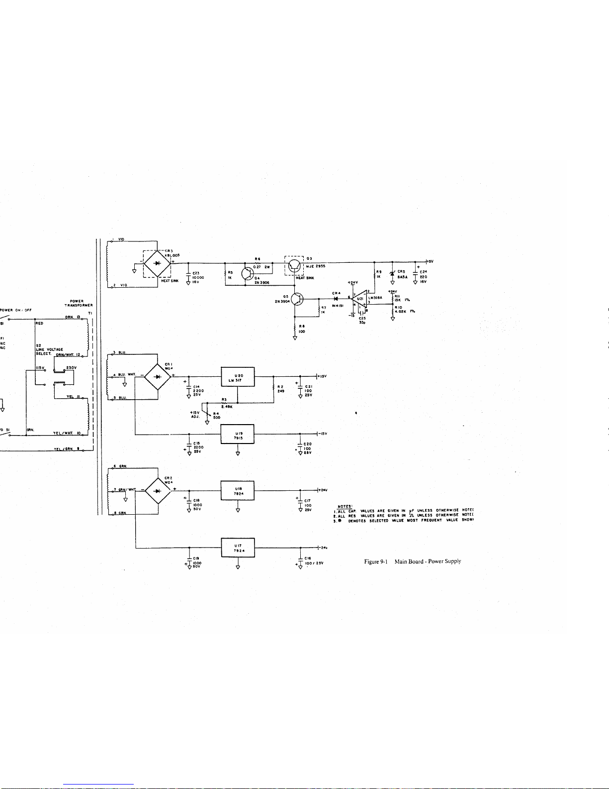
Page 96
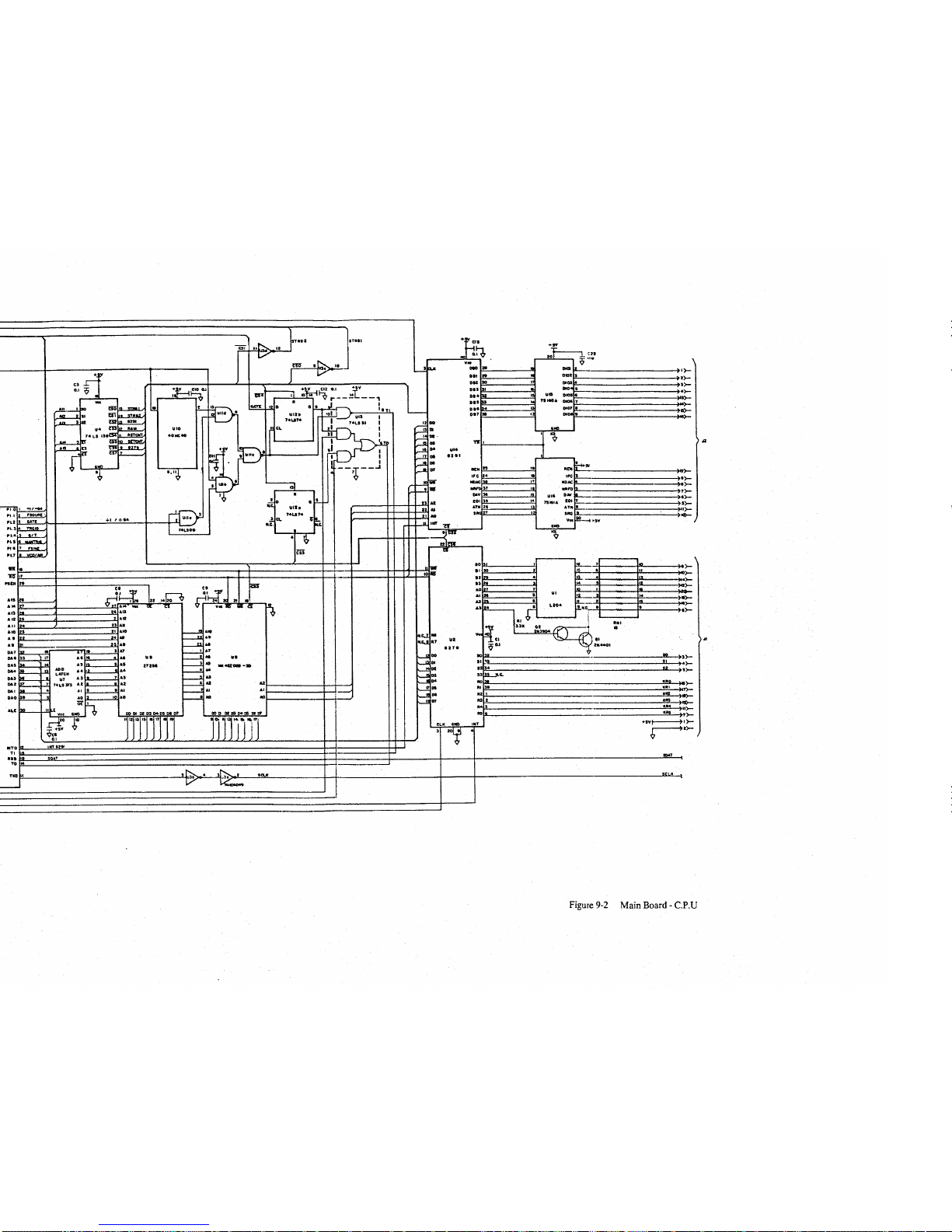
Page 97
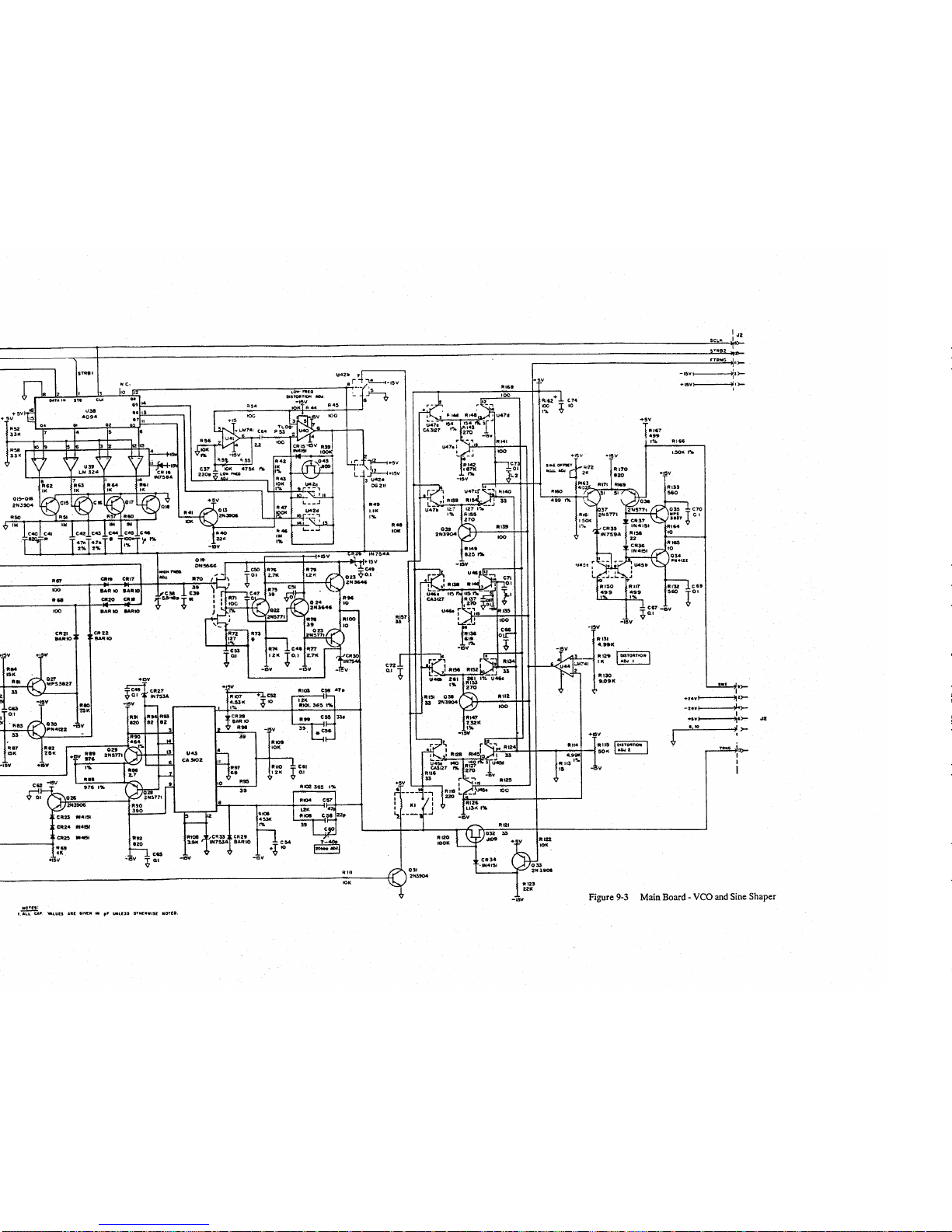
Page 98
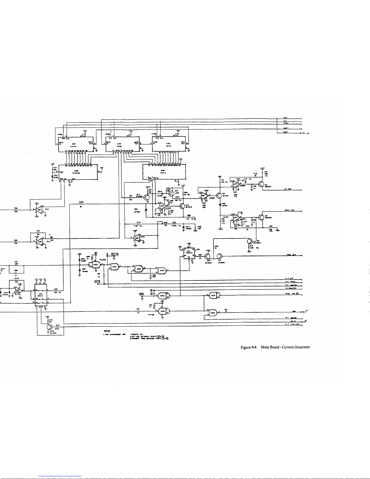
Page 99
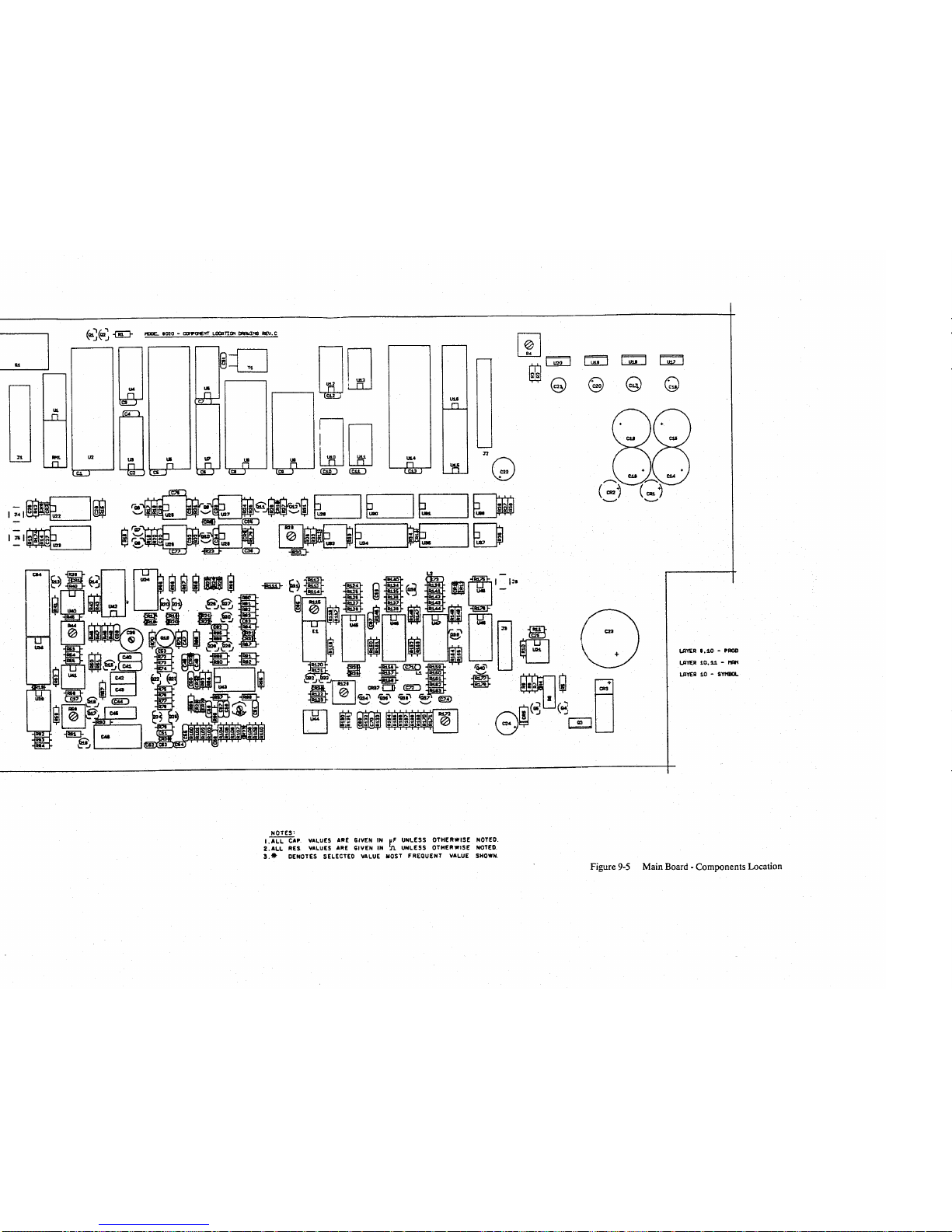
Page 100
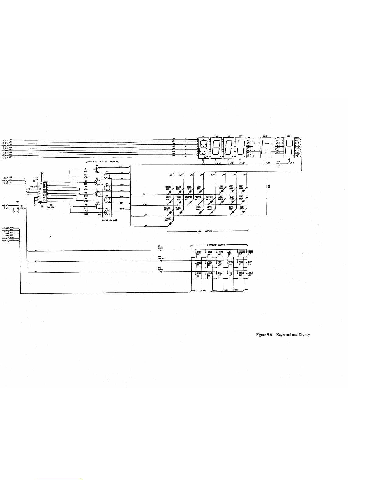
 Loading...