

Page 1
查询SG6849-100D供应商
Product Specification
Low-Power Green-Mode PWM Flyback Power Controller without Secondary Feedback SG6849
FEATURES
Linearly Decreasing PWM Frequency
Green-Mode under Light-Load and Zero-Load
Conditions
Constant Voltage (CV) and Constant Current (CC)
No Secondary Feedback
Low Startup Current (5uA)
Low Operating Current (3.6mA)
Leading-Edge Blanking
Constant Power Limit
Universal AC Input Range
Synchronized Slope Compensation
150°C OTP Sensor with Hysteresis
V
Over Voltage Clamping
DD
Cycle-by-Cycle Current Limiting
Under Voltage Lockout (UVLO)
Fixed PWM Frequency (65kHz/100kHz)
Gate Output Maximum Voltage Clamped at 16.7V
Small SOT-26 Package
APPLICATIONS
Low-power flyback power converters, such as
Battery chargers for cellular phones, cordless phones,
PDAs, digital cameras, and power tools.
Power adapters for ink jet printers, video game
consoles, and portable audio players.
Open-frame SMPS for TV/DVD standby and other
auxiliary supplies, home appliances, consumer
electronics, and PC 5V standby-power.
Replacements for linear transformers and RCC
SMPS.
DESCRIPTION
This highly integrated PWM controller provides several
features to enhance the performance of low power flyback
converters. To minimize standby power consumption, the
proprietary green-mode function provides off-time
modulation to linearly decrease the switching frequency
under light-load and zero-load conditions. This
green-mode function enables the power supply to easily
meet international power conservation requirements. The
supply voltage V
compensation, to regulate the output voltage without
requiring a conventional TL431 and a photo-coupler.
Another advantage of the SG6849 is that the typical
startup current is only 5uA, while the typical operating
current can be as low as 3.6mA. A large startup resistance
could be used to achieve even higher power conversion
efficiency. Built-in synchronized slope compensation
maintains the stability of peak current-mode control.
Proprietary internal compensation ensures constant output
power limiting over a universal range of AC input
voltages, from 90VAC to 264VAC.The SG6849 provides
many protection functions. Pulse-by-pulse current
limiting ensures a constant output current, even if a short
circuit occurs. Also, the internal protection circuit will
disable PWM output, if V
output is clamped at 16.7V to protect the power MOS
from over-voltage damage. The built-in over temperature
protection (OTP) function will shutdown the controller at
150°C with a 20°C hysteresis. The SG6849 is designed to
provide a low-cost total solution for flyback converters. It
is available in a small footprint, 6-pin, SOT-26 package.
is also used for feedback
DD
exceeds 22.7V. The gate
DD
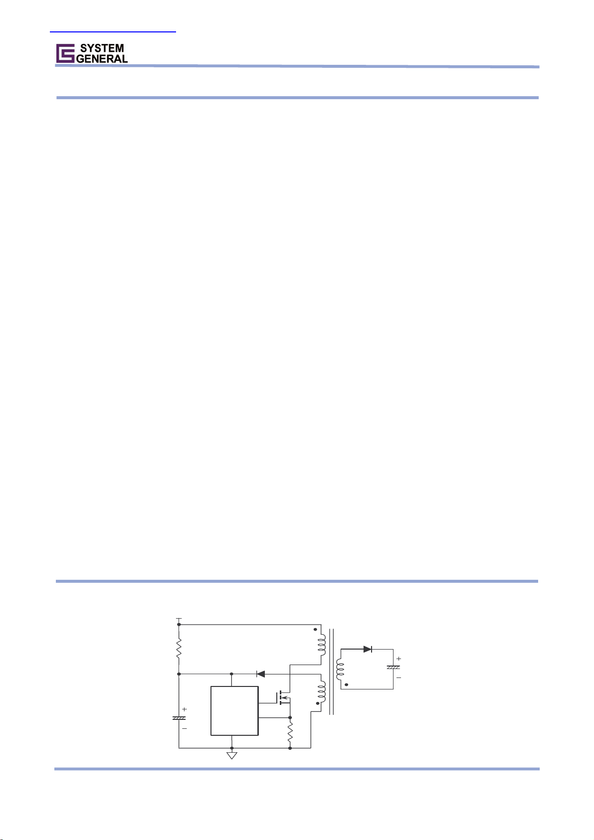
TYPICAL IC APPLICATION
R
CIN
VIN
D
IN
D
1
VDD
GND
GATE
SENSE
Q1
RS
W
AUX
O
C
O
V
O
© System General Corp. - 1 - www.sg.com.tw
Version 1.0(IRO33.0002.B3) Dec.29, 2003
Page 2
Product Specification
W
1
GN
WWV
N
Low-Power Green-Mode PWM Flyback Power Controller without Secondary Feedback SG6849
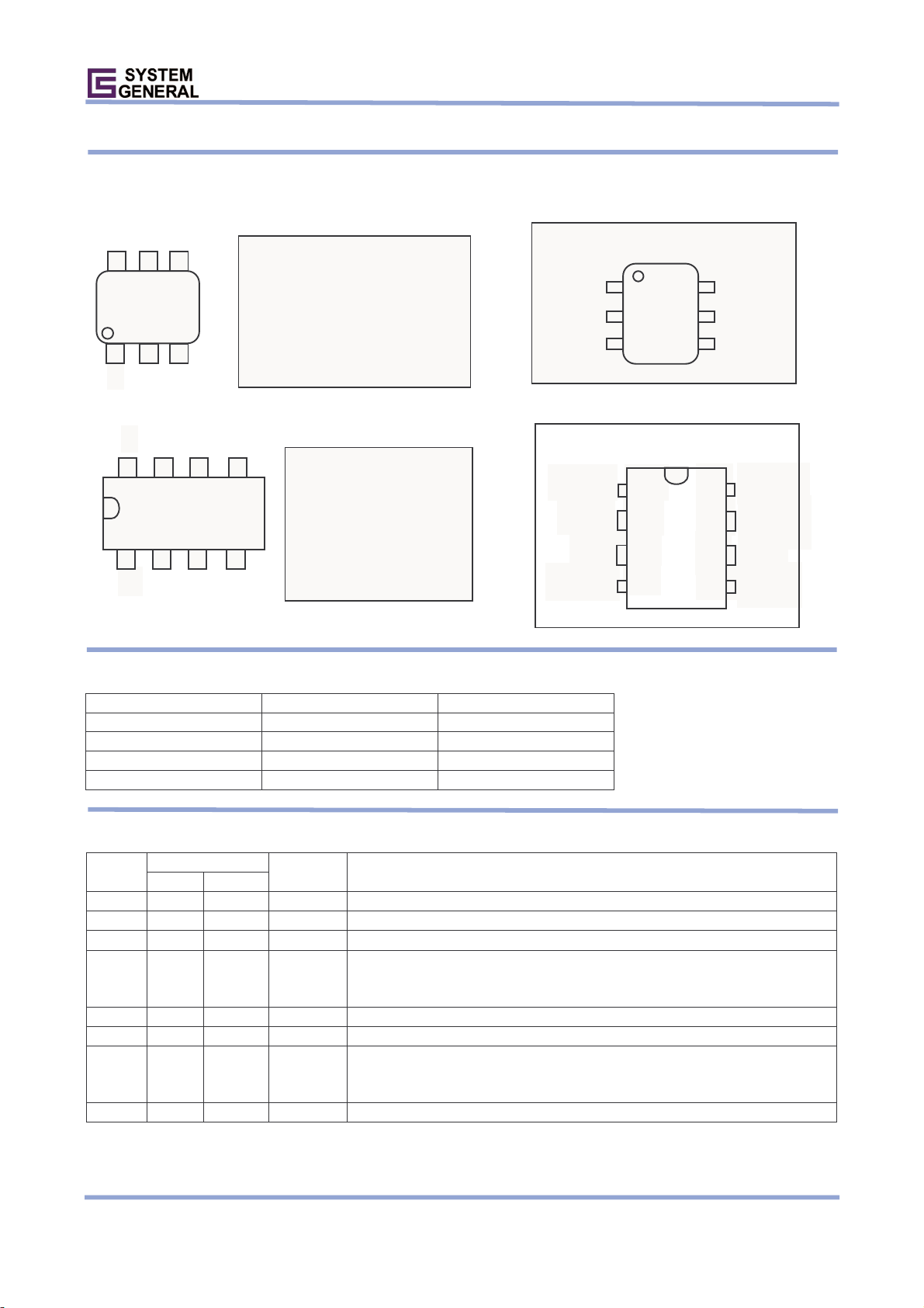
MARKING INFORMATION PIN CONFIGURATION
MXYWW
1
1
8
SG6849-ZZZD
XXXXXXXYY
M: Mask Version
X: B= SG6849-65T
C= SG6849-100T
Y: Year
W
: Work Week
ZZZ: 65 or 100
XXXXXXX: Wafer Lot
YY: Year
WW: Week
V: Assembly Location
D
FB
NC
GATE
VDD
SENSE
SOT-26
GATE
6
2
3
5
VDD
4
SENSE
DIP-8
GND
1
2
C
8
FB
7
6
NC
NC
5
ORDERING INFORMATION
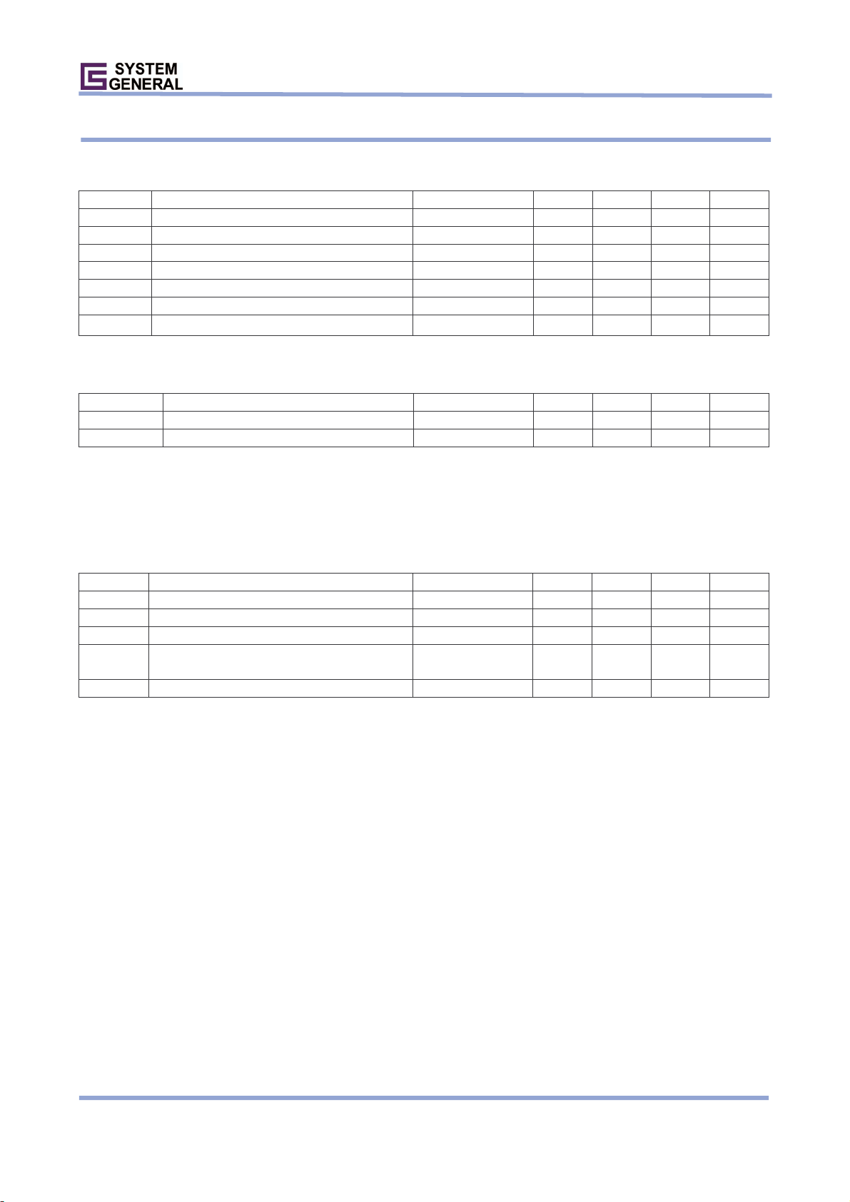
Part Number PWM Frequency Package
SG6849-65T 65kHz 6-Pin SOT-26
SG6849-100T 100kHz 6-Pin SOT-26
SG6849-65D 65kHz 8-pin DIP-8
SG6849-100D 100kHz 8-pin DIP-8
PIN DESCRIPTIONS
Name
GATE 1 6 Driver Output The totem-pole output driver to drive the power MOSFET.
VDD 2 5 Supply Power supply.
NC 3 NA NC pin.
SENSE 4 4 Analog Input
NC 5 3 NC pin.
NC 6 NA NC pin.
FB 7 2 Analog Input
GND 8 1 Supply Ground.
Pin No.
DIP-8 SOT-26
Type Function
Current s ense. It senses the voltage across a sensed r esistor. To provide over-c urrent
protection, PW M output is disabled if the voltage exceeds an internal thr eshold. This pin
also provides current information for current-mode control.
Feedback. The FB pin provides feedback information to the internal PWM compar ator.
This feedback is used to control the duty cycle. When no feedback is pr ovided, this pin is
left open.
© System General Corp. - 2 - www.sg.com.tw
Version 1.0(IRO33.0002.B3) Dec.29, 2003
Page 3
Product Specification
p
r
Low-Power Green-Mode PWM Flyback Power Controller without Secondary Feedback SG6849
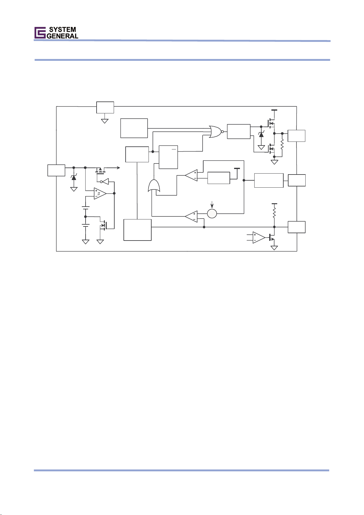
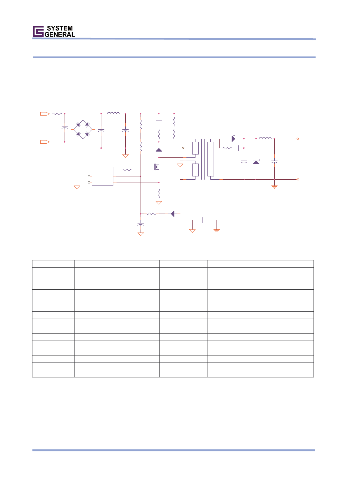
BLOCK DIAGRAM
GND
VDD
2(5)
DIP-8(SOT-26)
8(1)
Internal
Supply
UVLO
17V/8V
OTP
SENSE
OSC
Green
Mode
Controller
S
R
Q
OCP
Comp
PWM
Comp
Com
Powe
Limiter
Slope
ensation
Σ
Driver
V
DD
VDD
VDDZ
Blanking
Circuit
4.5V
V
DD
GATE
1(6)
SENSE
4(4)
FB
7(2)
© System General Corp. - 3 -
www.sg.com.tw
Version 1.0(IRO33.0002.B3) Dec.29, 2003
Page 4
Product Specification
Low-Power Green-Mode PWM Flyback Power Controller without Secondary Feedback SG6849
ABSOLUTE MAXIMUM RATINGS
Symbol Parameter Value Unit
DC Supply Voltage*
VDD
VFB FB Pin Input Voltage -0.3 to 7 V
V
SENSE
PD Power Dissipation 300 mW
RθJA Thermal Resistance (Junction to A ir)
RθJC Thermal R esistanc e (Junction to Case)
TJ Operating Junction Temperature 150 °C
T
STG
T
L
*All volt age values, except differential voltages, are given with respect to the network ground terminal.
Zener Clamp
Zener Current
Sense Pin Input Voltage -0.3 to 7 V
SOT-26
DIP-8
SOT-26
DIP-8
Storage Temperature Range -55 to +150 °C
Lead Temperature (Soldering)
ESD Capability, Human Body Model 3.0 kV
ESD Capability, Machine Model 300 V
20 sec SOT-26
10 sec DIP-8
25
30
10
243.3
113.0
115
67.1
220
260
V
V
mA
°C/W
°C/W
°C
OPERATING CONDITIONS
Symbol Parameter Value Unit
VDD DC Supply Voltage <22.7 V
TA Operating Ambient T emperature -30 to +85 °C
ELECTRICAL CHARACTERISTICS (V
=15V, TA=25°C)
DD
Feedback Input Section
Symbol Parameter Test Condition Min. Typ. Max. Unit
IOZ Zero Duty-Cycle FB Input C urrent 1.15 1.4 mA
VFB Open Loop Voltage 4.5 V
RFB Input Impedance FB Input Current = 0.1mA 2.4 kΩ
V
V
DDZ
*The feedback input is pulled by a transistor that is controlled by the VDD signal while VDD V
Feedback Threshold Voltage*
DD
FB Input Current = 0mA 20 22.7 25 V
FB Input Current = 0.8mA 18 20 22 V
≧
.
DDZ
© System General Corp. - 4 -
www.sg.com.tw
Version 1.0(IRO33.0002.B3) Dec.29, 2003
Page 5

Product Specification
Low-Power Green-Mode PWM Flyback Power Controller without Secondary Feedback SG6849
Current Sense Section
Symbol Parameter Test Condition Min. Typ. Max. Unit
TPD Propagation Delay 100 ns
VDD = 20V 0.84 0.89 0.94 V
VTH,VA
Current Limiting Valley Threshold Voltage for 65kHz
Current Limiting Valley Threshold Voltage for 100kHz
T
ON
VDD = 15V 0.72 0.77 0.82 V
VDD = 10V 0.58 0.63 0.68 V
VDD = 20V 0.76 0.81 0.86 V
VDD = 15V 0.65 0.70 0.75 V
VDD = 10V 0.52 0.57 0.62 V
V
V
Ramp
T
OFF
LIMIT
TH, FT
0.77V
High-Line
Sense Voltage
Low-Line Sense
Voltage
V
TH,V A
0V
T
1
T
2
Oscillator Section
Symbol Parameter Test Condition Min. Typ. Max. Unit
F
SG6849–65 Frequency 60 65 70 kHz
OSC
F
SG6849–100 Frequency 92 100 108 kHz
OSC
F
Green-Mode Burst Back Frequency* 20 25 30 kHz
OSC-G-BK
F
I
FB-G-OFF
FDV Frequenc y Variation versus VDD Deviation VDD = 10 to 20V 2 %
V
*Please see the “Green-Mode Burst B ack (F
Green-Mode OFF Frequency* 0 kHz
OSC-G-OFF
Green-Mode OFF FB Input Current 0.9 1.15 1.4 mA
DD-TH-G
V
OFF
) and Green-Mode OFF Frequency (F
OSC-G-BK
-Low Threshold Voltage for Exiting Green-Mode
DD
V
DD
+1.0
OFF
OSC-G-OFF
V
DD
+1.5
OFF
) vs. VDD” curves.
V
OFF
DD
+2.0
V
© System General Corp. - 5 -
www.sg.com.tw
Version 1.0(IRO33.0002.B3) Dec.29, 2003
Page 6
Product Specification
Low-Power Green-Mode PWM Flyback Power Controller without Secondary Feedback SG6849
Output Section
Symbol Parameter Test Condition Min. Typ. Max. Unit
DCY
Maximum Duty Cycle 70 75 80 %
MAX
Bnk Leading Edge Blanking Time 310 ns
VOL Output Voltage Low VDD = 15V, IO = 10mA 1.5 V
VOH Output Voltage High VDD = 15V, IO = 10mA 8 V
TR Rising Time VDD = 15V, CL = 1nF 200 ns
TF Falling Time VDD = 15V, CL = 1nF 80 ns
V
Output Clamp Voltage VDD = 20V 16.7 18 V
CLAMP
Over Temperature Protection (OTP)
Symbol Parameter Test Condition Min. Typ. Max. Unit
Temp-Off Protection Junction Temperature*1 150 °C
Temp-Restart Restart Junction Temperature*2 130 °C
*1
When activated, the output is disabled and the latch is turned off.
*2
This is the threshold temperature for enabling the output again and resetting the latch, after over temperat ure protection has been
activated.
VDD Section
Symbol Parameter Test Condition Min. Typ. Max. Unit
V
Turn-On Threshold Voltage 16 17 18 V
DD ON
V
Turn-Off Threshold Voltage 7.5 8 8.5 V
DD OFF
I
Startup Current VDD = 15V 5 30 uA
DD ST
V
= 15V
I
Operating Supply Current
DD OP
V
Zener Diode Breakdown Voltage IDD = 10mA 28 30 V
DD CLAMP
DD
GATE is Open
3.6 6 mA
© System General Corp. - 6 -
www.sg.com.tw
Version 1.0(IRO33.0002.B3) Dec.29, 2003
Page 7
Product Specification
)
Low-Power Green-Mode PWM Flyback Power Controller without Secondary Feedback SG6849
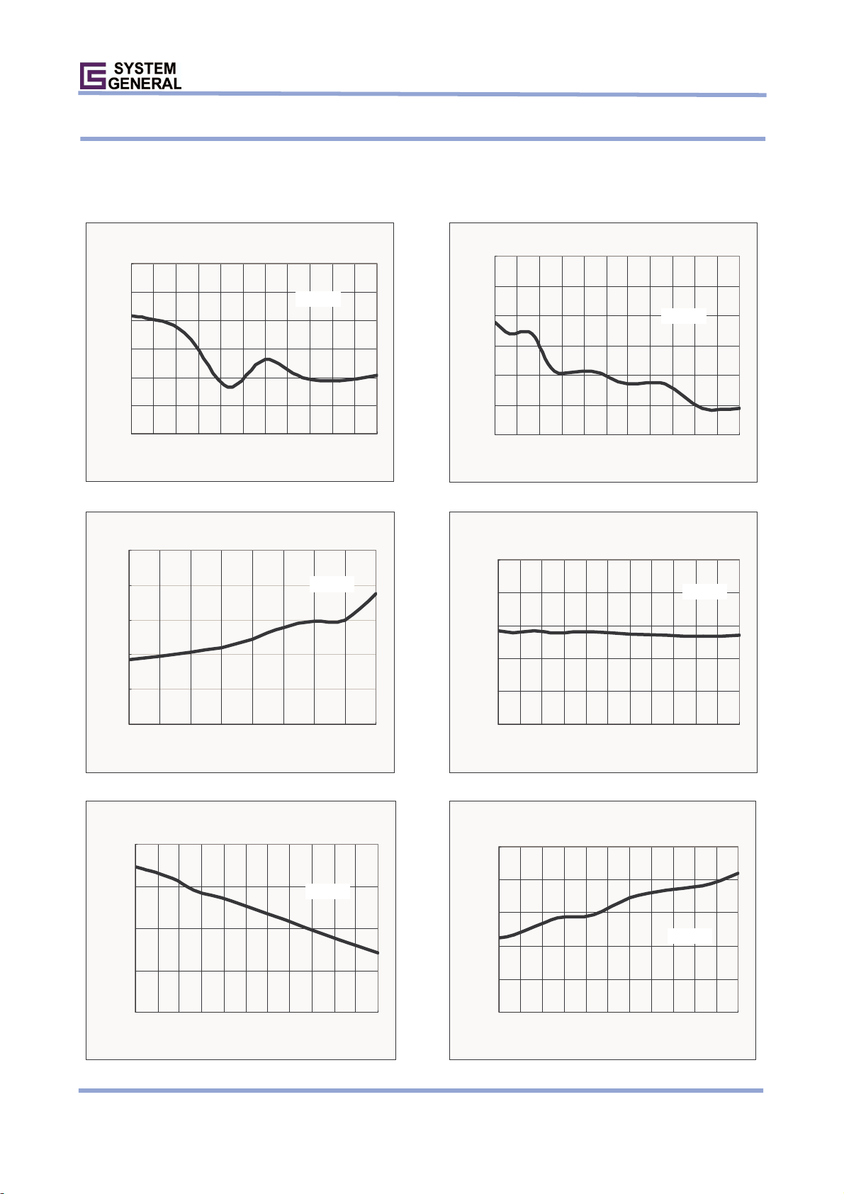
TYPICAL CHARACTERISTICS
SG6849-65
Start-Up Current (I
9.0
8.0
7.0
(uA )
6.0
DD ST
I
5.0
4.0
3.0
-40 -25 -10 5 20 35 50 65 80 95 110 125
TEMPERATURE (℃)
) vs. Temp er atu r e
DD ST
VDD=15. 0V
VFB Open Loop Voltage (VFB) vs. Temperature
5. 0
4. 8
4. 6
(V)
FB
V
4. 4
VDD=15.0V
Operating Supply Current (I
4.5
4.3
4.0
(mA )
3.8
DD OP
I
3.5
3.3
3.0
-40 -25 -10 5 20 35 50 65 80 95 110 125
TEMPERATURE (℃)
Maximum Duty Cycle (DCY
80.0
78.0
76.0
(%)
MAX
74.0
DCY
) vs. Temp er atu r e
DD OP
VDD=15.0V
) vs. Temper at ur e
MAX
VDD=15.0V
4. 2
4. 0
-40 -30 -15 0 25 50 75 100 125
TEMPERA TURE (℃)
Oscillator Frequency (F
70.0
65.0
(kHz
60.0
OSC
F
55.0
50.0
-40 -25 -10 5 20 35 50 65 80 95 110 125
TEMPERATURE (℃)
) vs. Temperature
OSC
VDD=15. 0V
72.0
70.0
-40 -25 -10 5 20 35 50 65 80 95 11 0 125
TEMPERATURE (℃)
Valley Threshold Voltage (V
0.80
0.78
0.76
(V)
TH,VA
V
0.74
0.72
0.70
-40 -25 -10 5 20 35 5 0 65 80 95 11 0 125
TEMPERATURE (℃)
) vs. Temper at ur e
TH,VA
VDD=15.0V
© System General Corp. - 7 -
www.sg.com.tw
Version 1.0(IRO33.0002.B3) Dec.29, 2003
Page 8
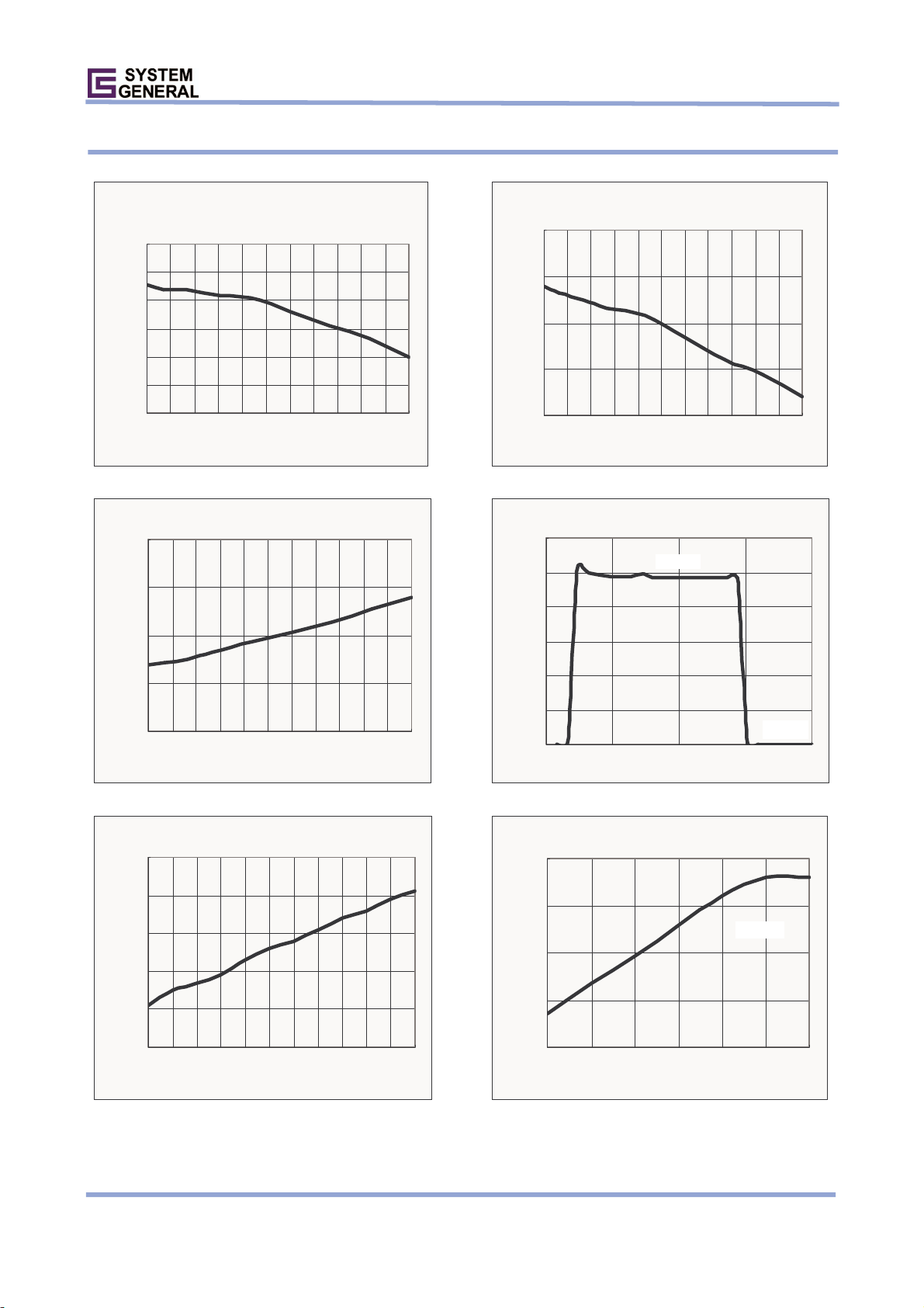
Product Specification
)
Low-Power Green-Mode PWM Flyback Power Controller without Secondary Feedback SG6849
Turn-On Thr eshold Vol tage (V
Temperature
18.0
17.5
17.0
(V)
16.5
DD ON
V
16.0
15.5
15.0
-40 -25 -10 5 20 35 50 65 80 95 110 125
TEMPERATURE (℃)
DD O N
) vs.
Output Voltage Low (VOL) vs. Temperature
0.40
0.30
(V)
0.20
OL
V
0.10
(V)
DD OFF
V
(k Hz
OSC
F
Turn-Off Threshold Voltage (V
Temperature
9.00
8.50
8.00
7.50
7.00
-40 -25 -10 5 20 35 50 65 80 95 110 125
TEMPERATURE (℃)
Green-Mode Bu rst B ack(F
OFF Frequency(F
30.0
25.0
20.0
15.0
10.0
F
OSC-G-BK
OSC-G-BK
OSC-G-OFF
) vs.
DD OFF
) and Green-Mode
) vs. V
DD
0.00
-40-25-10 5 203550658095110125
TEMPERATURE (
Valley Threshold Voltage(V
1.00
0.90
0.80
(V)
TH,VA
V
0.70
0.60
0.50
9 1011121314151617181920
℃
)
) vs. V
TH,VA
V
(V)
DD
5.0
F
OSC-G- OFF
0.0
88.599.510
DD
1.10
1.05
1.00
Vlimit (V)
0.95
0.90
10 15 20 25 30 35 40
V
LIMIT
V
(V)
DD
Ramp vs. Duty Cycle
Duty Cyc le (%)
VDD=15.0V
© System General Corp. - 8 -
www.sg.com.tw
Version 1.0(IRO33.0002.B3) Dec.29, 2003
Page 9

Product Specification
Low-Power Green-Mode PWM Flyback Power Controller without Secondary Feedback SG6849
OPERATION DESCRIPTION
SG6849 devices integrate many useful functions for low
power switch mode power supplies. The following
descriptions highlight the key features of the SG6849.
Startup Current
The required startup current is only 5uA. This allows a
high-resistance, low-wattage startup resistor to be used to
supply the controller’s startup power. A 1.5 MΩ/0.25W
startup resistor can be used over a wide input range
(100V-240V AC) with very little power loss.
Operating Current
The operating current is normally 3.6mA. The low
operating current results in higher efficiency and reduces
the required V
hold-up capacitor can be used over a wide input range
(100V-240V AC) with very little power loss.
hold-up capacitance. A 10uF/25V VDD
DD
Green Mode Operation
The proprietary green-mode function provides off-time
modulation to linearly decrease the switching frequency
under light-load and zero-load conditions. The on-time is
limited to provide better protection against brownouts and
other abnormal conditions.
This green-mode function dramatically reduces power
consumption under light-load and zero-load conditions.
Power supplies using the SG6849 can easily meet
international restrictions regarding standby
power-consumption.
Constant Voltage (CV) and Constant
Current (CC) without Feedback
Over Temperature Protection (OTP)
The SG6849 has a built-in temperature sensing circuit to
shut down PWM output once the junction temperature
exceeds 150°C. While PWM output is shut down, the V
voltage will gradually drop to the UVLO voltage. Some of
the SG6849’s internal circuits will be shut down, and V
will gradually start increasing again. When V
17V, all the internal circuits, including the temperature
sensing circuit, will start operating normally. If the
junction temperature is still higher than 150°C, the PWM
controller will be shut down immediately. This situation
will continue until the temperature drops below 130°C.
The PWM output will then be turned back on. The
temperature hysteresis window for the OTP circuit is
20°C.
DD
DD
DD
reaches
VDD Over Voltage Clamping
VDD over voltage clamping is built in to prevent damage
from over-voltage conditions. When V
PWM output is shut down. Over-voltage conditions may
be caused by an open photo-coupler loop or a short circuit
in the output.
exceeds 22.7V,
DD
Oscillator Operation
The oscillation frequency is fixed at 65kHz for the
SG6849-65, and at 100kHz for the SG6849-100.
Leading Edge Blanking
Each time the power MOSFET is switched on, a turn-on
spike will inevitably occur at the sense-resistor. To avoid
premature termination of the switching pulse, a 310ns
leading-edge blanking time is built in. Conventional RC
filtering is not necessary. During this blanking period, the
current-limit comparator is disabled, and it cannot switch
off the gate drive.
The SG6849 can tightly regulate the output voltage and
provide over current protection without requiring
secondary-side feedback signals. For improved CV and
CC accuracy, the transformer leakage inductance should
be reduced as much as possible.
© System General Corp. - 9 -
Version 1.0(IRO33.0002.B3) Dec.29, 2003
Constant Output Power Limit
When the SENSE voltage across the sense resistor RS
reaches the threshold voltage (around 1.0V), the output
GATE drive will be turned off following a small
www.sg.com.tw
Page 10

Product Specification
×
Low-Power Green-Mode PWM Flyback Power Controller without Secondary Feedback SG6849
propagation delay TPD. This propagation delay will
introduce an additional current proportional to
T
PD*VIN/LP
regardless of the input line voltage V
. The propagation delay is nearly constant
. Higher input line
IN
voltages will result in larger additional currents. Thus,
under high input-line voltages the output power limit will
be higher than under low input-line voltages.
Over a wide range of AC input voltages, the variation can
be significant. To compensate for this, the threshold
voltage is adjusted by adding a positive ramp. This ramp
signal can vary from 0.77V to 1.05V for SG6849-65 and
0.70 to 1.03V for SG6849-100, and it flattens out at 1.05V
and 1.03V respectively. A smaller threshold voltage
forces the output GATE drive to terminate earlier, thus
reducing total PWM turn-on time and making the output
power equal to that of the low line input. This proprietary
internal compensation feature ensures a constant output
power limit over a wide range of AC input voltages
(90VAC to 264VAC).
Under Voltage Lockout (UVLO)
The turn-on/turn-off thresholds of the SG6849 are fixed
internally at 17V/8V. To enable the SG6849 during
startup, the hold-up capacitor must first be charged to 17V
through the startup resistor.
The hold-up capacitor will continue to supply V
energy can be delivered from the auxiliary winding of the
main transformer. V
must not drop below 8V during
DD
this startup process. This UVLO hysteresis window
ensures that the hold-up capacitor can adequately supply
V
during startup.
DD
before
DD
Gate Output
The SG6849 BiCMOS output stage is a fast totem pole
gate driver. Cross-conduction has been avoided to
minimize heat dissipation, increase efficiency, and
enhance reliability. The output driver is clamped by an
internal 16.7V Zener diode in order to protect the power
MOSFET transistors against any harmful over-voltage
gate signals.
Slope Compensation
The sensed voltage across the current sense resistor is
used for current mode control and pulse-by-pulse current
limiting. The built-in slope compensation function
improves power supply stability. Furthermore, it prevents
sub-harmonic oscillations that normally would occur
because of peak current mode control. A positively sloped,
synchronized ramp is activated by the SG6849 with every
switching cycle. The slope of the ramp is
33.0
Duty
.
(max)
Duty
Noise Immunity
Noise from the current sense or the control signal may
cause significant pulse width jitter, particularly in
continuous-conduction mode. Slope compensation helps
alleviate this problem. Good placement and layout
practices should be followed. The designer should avoid
long PCB traces and component leads. Compensation and
filter components should be located near the SG6849.
Finally, increasing the power-MOS gate resistance is
advised.
© System General Corp. - 10 -
www.sg.com.tw
Version 1.0(IRO33.0002.B3) Dec.29, 2003
Page 11
Product Specification
Low-Power Green-Mode PWM Flyback Power Controller without Secondary Feedback SG6849
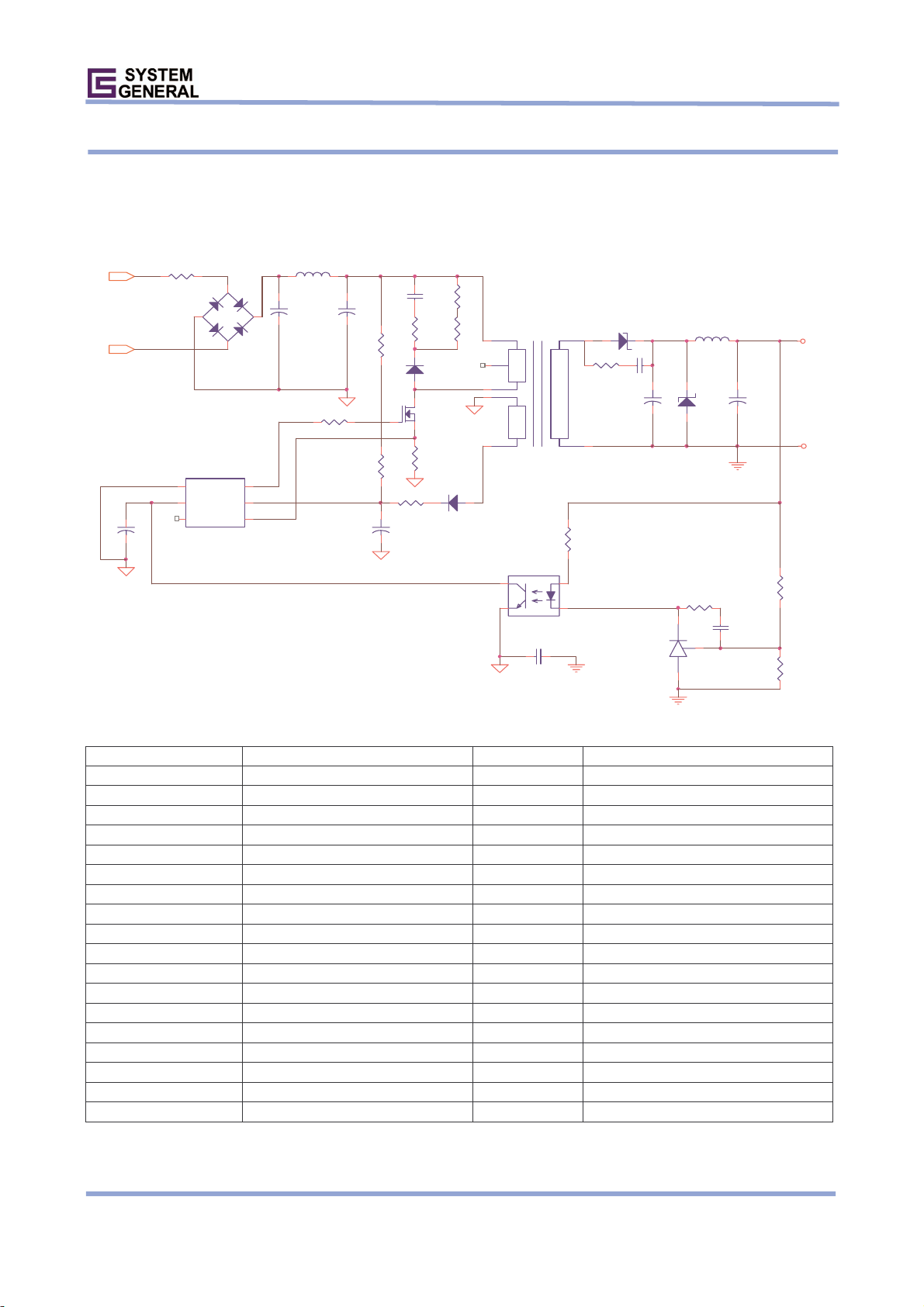
REFERENCE CIRCUIT
3W Flyback 5V/0.6A Circuit, without Secondary-Side Feedback
L
N
F1
CX1
1
BD1
-+
2
3
U4
1
2
3 4
SG6849
1 2
4
C1
GND
GATE
FB
VDD
NC SENSE
L1
R3
1
R8
C3
R4
9
8
5
7 3,4
21
T1
CY1
R5
D1
2 1
23
Q1
R6
D2
1,210
2 1
R10
D4
C8
C7
+
L2
1 2
D5
2 1
R1
+
C2
R2
R7
6
5
+
C4
BOM
Symbol Component Symbol Component
BD1 BD 1A/500V L1 20mH 6*8mm
CX1 (O ption) YC 472pF/400V (Y1) L2 10uH 6mm
CY1 (O ption) YC 102pF/400V (Y1) Q1 MOSFET 1A/600V
C2 EC 10uF/400V 105℃ R1,R2 R 750kΩ 1206
C1 CC 103pF/500V R3,R4 R 47kΩ 1206
C3 CC 1000pF/500V R5 R 47Ω 1206
C4 EC 10uF/50V R6 R 4.7Ω 1206
C7 (Option) CC 102pF/100V 1206 R7 R 100Ω 0805
C8 EC 470uF/10V 105℃ R8 R 10Ω 1206
C9 EC 220uF/10V 105℃ R10 (Option) R 10Ω 1206
D1 Diode FRI07 T1 EE-16
D2 Diode FR102 U4 IC SG6849 (Green PWM IC)
D4 Diode SB360
D5 (Option) ZD 6.8V 0.5W
F1 R 1Ω/0.5W
VO
+
C9
GND
© System General Corp. - 11 -
Version 1.0(IRO33.0002.B3) Dec.29, 2003
www.sg.com.tw
Page 12
Product Specification
Low-Power Green-Mode PWM Flyback Power Controller without Secondary Feedback SG6849
3W Flyback 5V/0.6A Circuit, with Secondary-Side Feedback
L
N
F1 L1
-+
2
U1
SG6849
1
GND
2
FB
3 4
C6
NC SENSE
1
3
GATE
VDD
BD1
6
5
4
1 2
+
C1
C3
+
C2
R1
2 1
R7
23
1
R2
R8
+
C4
R3
R4
R5 T1
D1
Q1
R6
D2
9
8
5
7 3,4
21
4
3
U2
CY1
1,210
D4
2 1
R10
C7
+
C8
L2
1 2
2 1
Vo
+
C9D5
GND
R11
1
2
R14
3
2
C10
U3
1
R13
R12
BOM
Symbol Component Symbol Component
BD1 (Reference only) DI106 1A/600V L2 10uH 6mm
CY1 (Option) YC 102p/400V
C2 10uF/400V 10Φ*16mm 105℃ R1,R2 750k 1206
C1 103p/500V (0.01uF/500V) R4,R3 47k/1206
C3 1000p/500V CER R5 47 1206
C4 10u/50V 5mm R6 3.7 1206
C6 472p 0805 R7 100 0805
C7 102p/100V 1206 R10 10 1206
C8 470u/10V 8Φ*11.5mm 105 ℃ R8 5 1206
C9 470u/10V 8Φ*11.5mm 105℃ R11 100 1/8W
C10 222p 0805 R12 33k 0805
D1 FR107 R13 33k 1/8W
D2 FR102 R14 4.7k 0805
D4 SB360 (3A/60V; Schottky) T1 EE-16
D5 (Option) ZD/6.8V 0.5W U1 SG6849 (Gr een PWM IC)
F1 1Ω1/2W Resistor U2 PC817
L1 20mH 6*8mm U3 TL431
BD1 (Reference only) DI106 1A/600V L2 10uH 6mm
Q1 MOSFET 1A/600V
© System General Corp. - 12 -
www.sg.com.tw
Version 1.0(IRO33.0002.B3) Dec.29, 2003
Page 13
Product Specification
A
A
A
Low-Power Green-Mode PWM Flyback Power Controller without Secondary Feedback SG6849
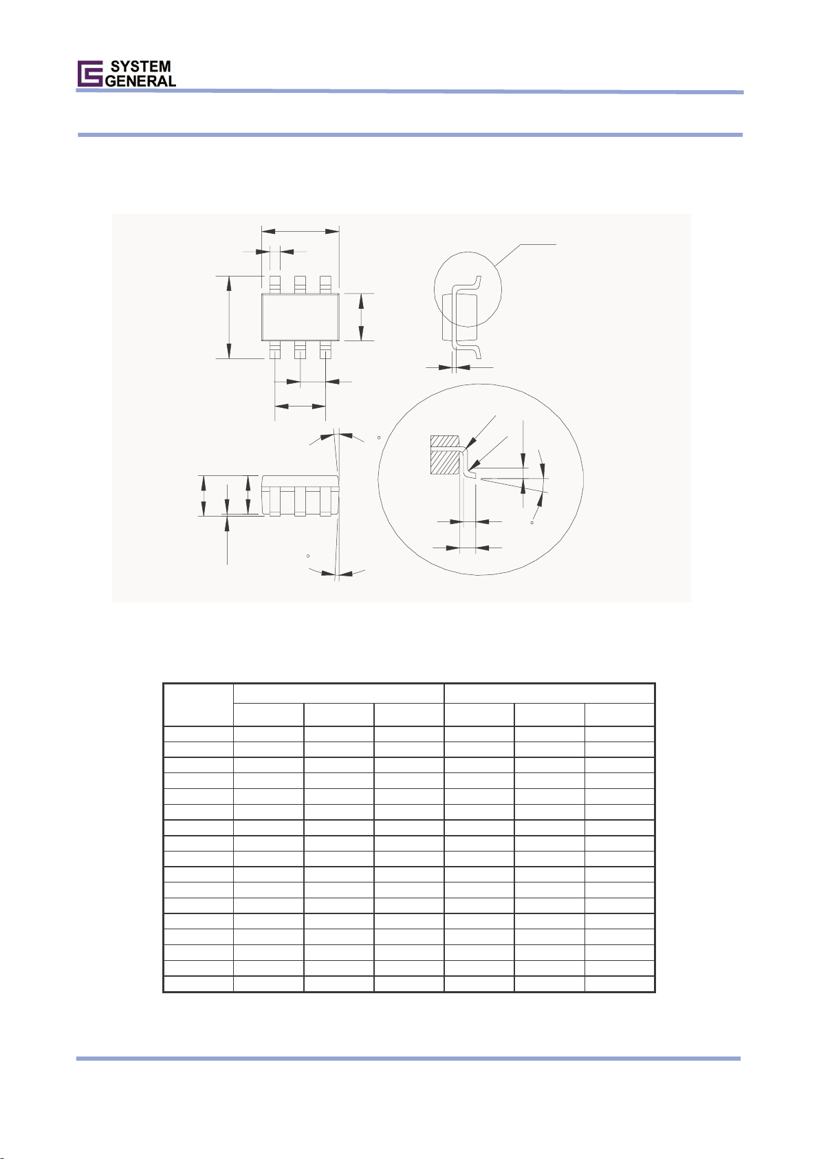
PACKAGE INFORMATION
The SOT-26 Package
D
b
64
Detail A
Dimensions:
Symbol
b 0.30 0.50 0.011 0.020
c 0.08 0.22 0.003 0.009
D 2.90 0.114
E 2.80 0.110
E1 1.60 0.063
e 0.95 0.037
e1 1.90 0.075
L 0.30 0.45 0.60 0.020 0.018 0.24
L1 0.60 0.024
L2 0.25 0.010
R 0.10 0.004
R1 0.10 0.25 0.004 0.25
θ˚ 0˚ 4˚ 8˚ 0˚ 4˚ 8˚
θ1˚ 5˚ 10˚ 15˚ 5˚ 10˚ 15˚
E
1
e
e1
A
A1
A2
θ
1
E1
3
θ
1
c
R
L
L1
Detail A
1
L2
R
θ
Millimeters Inches
Min. Typ. Max. Min. Typ. Max.
1.45 0.057
1 0.15 0.006
2 0.90 1.15 1.30 0.036 0.045 0.051
© System General Corp. - 13 -
Version 1.0(IRO33.0002.B3) Dec.29, 2003
www.sg.com.tw
Page 14

Product Specification
A
A
A
Low-Power Green-Mode PWM Flyback Power Controller without Secondary Feedback SG6849
The DIP-8 Package
D
°
85
Θ
E1
41
A2
A1
L
b1
e
b
E
A
eB
Dimensions:
Symbol
5.334 0.210
1 0.381 0.015
2 3.175 3.302 3.429 0.125 0.130 0.135
b 1.524 0.060
b1 0.457 0.018
D 9.017 9.271 10.160 0.355 0.365 0.400
E 7.620 0.300
E1 6.223 6.350 6.477 0.245 0.250 0.255
e 2.540 0.100
L 2.921 3.302 3.810 0.115 0.130 0.150
e
8.509 9.017 9.525 0.335 0.355 0.375
θ˚ 0 7 15 0 7 15
Millimeter Inch
Min. Typ. Max. Min. Typ. Max.
© System General Corp. - 14 -
Version 1.0(IRO33.0002.B3) Dec.29, 2003
www.sg.com.tw
Page 15

Product Specification
Low-Power Green-Mode PWM Flyback Power Controller without Secondary Feedback SG6849
DISCLAIMERS
LIFE SUPPORT
System General’s products are not designed to be used as components in devices intended to support or sustain human life.
Use of System General’s products in components intended for surgical implant into the body, or other applications in
which the failure of System General’s products could create a situation where personal death or injury may occur, is not
authorized without the express written approval of System General’s Chief Executive Officer. System General will not be
held liable for any damages or claims resulting from the use of its products in medical applications.
MILITARY
System General's products are not designed for use in military applications. Use of System General’s products in military
applications is not authorized without the express written approval of System General’s Chief Executive Officer. System
General will not be held liable for any damages or claims resulting from the use of its products in military applications.
RIGHT TO MAKE CHANGES
System General reserves the right to change this document and/or this product without notice. Customers are advised to
consult their System General sales representative before ordering.
© System General Corp. - 15 -
Version 1.0(IRO33.0002.B3) Dec.29, 2003
www.sg.com.tw
 Loading...