

Page 1
PC Power Supply Supervisors SG6510X1
Product Specification
FEATURES
Over-voltage protection (OVP) for 3.3V, 5V and
12V
Under-voltage sense (UVS) and protection (UVP)
for 3.3V, 5V
Open drain output for PGO and FPO pins
300mS power good delay
75mS turn on delay for 3.3V and 5V
2.8mS PSON control to FPO turn-off delay
38mS /38mS PSON control De-bounce
350uS width noise deglitches
2mS UVP De-bounce time
1mS UVS De-bounce time
No lockup during the fast AC power on/off
Brownout protection function for 3.3V and 5V
Wide supply voltage range from 4V to 15V
DESCRIPTION
SG6510 is designed to provide the voltage
supervisor function, remote on/off PSON function, power
good (PGO) indicator function, and fault protection (FPO)
function for switching power systems.
via VDD pin); under voltage sense (UVS) monitoring for
3.3V and 5V; and under voltage protection (UVP)
monitoring for 3.3V and 5V. When 3.3V or 5V voltage is
decreasing to 2.8V and 4.2V respectively, the under
voltage sense (UVS) function will be enabled to reset the
PGO signal from high to low. If 3.3V or 5V voltage is
further decreasing to 2.5V and 3.6V respectively, FPO
will be set to high to turn off the PWM controller IC. To
achieve better immunity for lighting surge glitch and to
prevent accidental power shut down during dynamic
loading condition, the de-bounce time for UVP and UVS
is 2mS/1mS respectively. The deglitch time for OVP is
75uS for better noise immunity. During AC sag or
brownout situation, the UVP functions still can be enabled
to protect power supply in case of output short circuit.
The power supply is turned on after 38mS de-bounce
time when PSON signal is set from high to low. To turn
off power supply, PSON signal is set from low to high and
the de-bounce time is 38mS. The PGI circuitry provides a
sufficient power-down warning signal for PGO. When
PGI input is lower than the internal 1.2V reference
voltage, after 350uS de-bounce time, the PGO signal is
pulled low.
For supervisor function, it provides the over voltage
protection (OVP) monitoring for 3.3V, 5V and 12V (12V
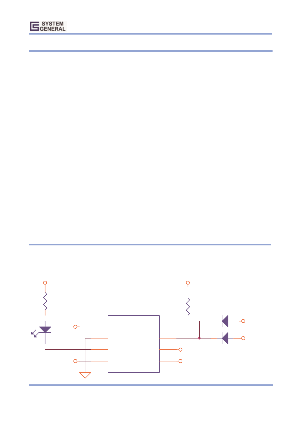
TYPICAL APPLICATION
5V
SG6510
PGI
PSON 3.3V
1
PGI
2
GND
3
FPO
4 5
PSON VS33
PGO
VDD
VS5
5V
8
7
6
5V
12V
5VSB
© System General Corp. - 1 - www.sg.com.tw
Version 1.0 ( IRO33.0025.B0) Feb.27,2004
Page 2

WWV
PC POWER SUPPLY SUPERVISORS SG6510X1
Product Specification
MARKING INFORMATION PIN CONFIGURATION
8
T: D = DIP
PGI
1
8
PGO
SG6510T1
XXXXXXXYY
1
XXXXXXX: Wafer Lot
YY: Year; WW: Week
V: Assembly Location
GND
FPO
PSON
2
3
4
7
6
5
VDD
VS5
VS33
ORDERING INFORMATION
Part Number Package Type
SG6510D1 8 pins DIP Plastic
PIN DESCRIPTIONS
Pin No. Pin Name
1 PGI Analog input Power good input . For AT X SMPS, it detects main AC voltage under-voltage and/or failure.
2 GND Supply Ground.
3 FPO Logic output
4 PSON Logic input
5 VS33 Analog input 3.3 V over/under-voltage c ontrol sense input.
6 VS5 Analog input 5 V over/under- voltage control sense input.
7 VDD Supply
8 PGO Logic output
Type Description
Fault protection output (invert). Output signal to control the PWM IC. For example it
controls the PW M IC of primary side through an opto-coupler. When FPO is low, the
main SMPS is operational.
Remote On/Off logic input from CPU or main-board. Turn on/off the PW M output after
38mS / 38mS delay.
Supply voltage. 4V ~ 15V. For AT X SMPS, it is c onnected to 5V-standby and 12V through
diodes respectively.
Power good logic output, 0 or 1(open-drain). P ower good=1 means that the power is
good for operation. The power good delay is 300mS.
© System General Corp. - 2 - www.sg.com.tw
Version 1.0 ( IRO33.0025.B0) Feb.27,2004
Page 3
Product Specification
PC POWER SUPPLY SUPERVISORS SG6510X1
FUNCTION TABLE
PGI PSON
PGI<1.2V L No No No L L
PGI<1.2V L Yes No No L L
PGI<1.2V L No Yes No L L
PGI<1.2V L No No Yes H L
PGI<1.2V L Yes Yes No L L
PGI<1.2V L Yes No Yes H L
PGI<1.2V L No Yes Yes H L
PGI<1.2V L Yes Yes Yes H L
PGI>1.2V L No No No L H
PGI>1.2V L Yes No No L L
PGI>1.2V L No Yes No H L
PGI>1.2V L No No Yes H L
PGI>1.2V L Yes Yes No H L
PGI>1.2V L Yes No Yes H L
PGI>1.2V L No Yes Yes H L
PGI>1.2V L Yes Yes Yes H L
X H X X X H L
UV Sense
(3.3V or 5V)
UV Protection
(3.3V or 5V)
OV Protection FPO PGO
x = don’t care
FPO = L means: fault IS NOT latched
FPO = H means: fault IS latched
PGO = L means: fault
PGO = H means: No fault
© System General Corp. - 3 - www.sg.com.tw
Version 1.0 ( IRO33.0025.B0) Feb.27,2004
Page 4
PC POWER SUPPLY SUPERVISORS SG6510X1
Product Specification
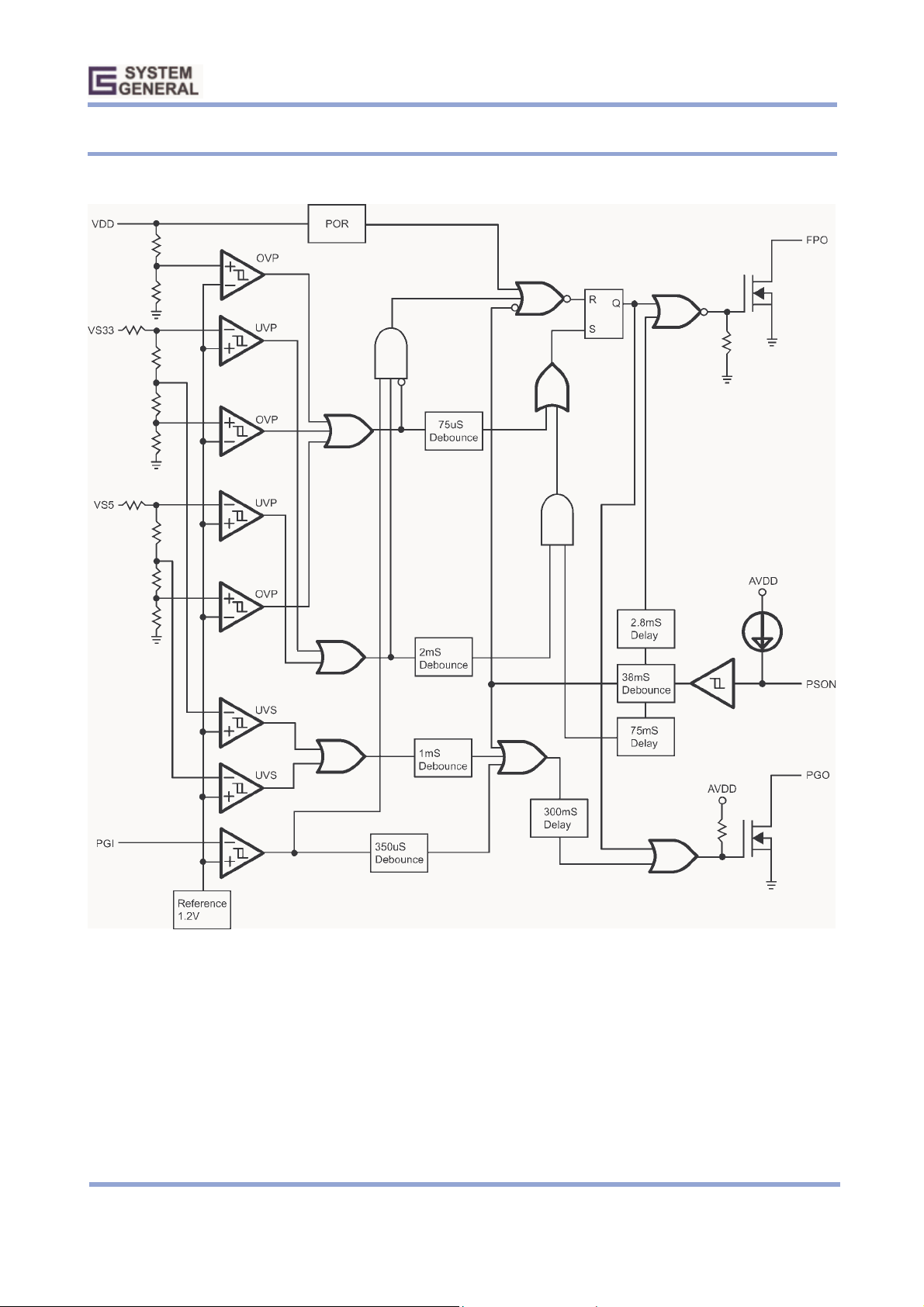
BLOCK DIAGRAM
© System General Corp. - 4 - www.sg.com.tw
Version 1.0 ( IRO33.0025.B0) Feb.27,2004
Page 5

PC POWER SUPPLY SUPERVISORS SG6510X1
Product Specification
TIMING DIAGRAM
© System General Corp. - 5 - www.sg.com.tw
Version 1.0 ( IRO33.0025.B0) Feb.27,2004
Page 6

Product Specification
PC POWER SUPPLY SUPERVISORS SG6510X1
ABSOLUTE MAXIMUM RATINGS
Symbol Parameter Min. Max. Unit
VDD DC Supply Voltage -0.3 16 V
Vi Input Voltage PSON, VS33, VS5, PGI -0.3 8 V
V
Output Voltage
OUT
TA Operating Free Air T emperature Range -40 85 ℃
T
Storage Temperature Range -55 150 ℃
STG
Soldering Temperature 260 ℃
ESD Capability, HBM model 2 KV
FPO -0.3 16
PGO -0.3 8
V
Note: Stresses above those listed may cause permanent damage to the device.
RECOMMENDED OPERATING CONDITIONS
Symbol Parameter Min. Max. Unit
VDD DC Supply Voltage 4 15 V
VIL Input Voltage PSON, VS33, VS5, PGI 7 V
V
Output Voltage
OUT
IoSINK Output Sink Current
TR Supply Voltage Rising Time See Note 1 mS
TA Operating Free Air Temperatur e Range -30 85 ℃
FPO 15
PGO 7
FPO 20
PGO 10
V
mA
Note: VDD rising and falling slew rate must be less than 14V/mS.
ELECTRICAL CHARACTERISTICS (VDD=12V, TA=25℃)
Over-voltage Protection
Symbol Parameter Test Conditions Min. Typ. Max. Unit
V
OVP
I
LKG
V
OL
T
Timing OVP to Pr otection 33 75 110 uS
OVP
Over-voltage Protection VS33 3.7 3.9 4.1
Over-voltage Protection VS5 5.7 6.1 6.5
Over-voltage Protection VDD 13.2 13.8 14.4
Leakage Current (FPO) V(FPO) = 5V 5 uA
Low Level Output Voltage (FPO) I
20mA 0.7 V
sink
V
© System General Corp. - 6 - www.sg.com.tw
Version 1.0 ( IRO33.0025.B0) Feb.27,2004
Page 7

Product Specification
PC POWER SUPPLY SUPERVISORS SG6510X1
Under-voltage and PGI, PGO
Symbol Parameter Test Conditions Min. Typ. Max. Unit
V
Input Threshold Volt age PGI 1.15 1.2 1.25 V
PGI
V
UVS
V
UVP
T
Timing UVS to Sense (PG) 0.6 1 1.5 mS
UVS
T
Timing UVP to Protection (FPO) 1.3 2 3 mS
UVP
I
Leakage C urrent (PGO) PGO = 5V 5 uA
LKG
VOL Low Level Output Voltage (PGO)
Under-voltage Enable Delay Time 49 75 114 mS
TPG
Under-voltage Sense VS33 2.6 2.8 3.0
Under-voltage Sense VS5 4.0 4.2 4.4
Under-voltage Protection VS33 2.3 2.5 2.7
Under-voltage Protection VS5 3.4 3.6 3.8
VDD = 12V
Isink 10mA
Timing PG Delay PGI to PGO 200 300 450 mS
Noise D eglitch Time PGI to PGO 200 350 450 uS
0.7 V
V
V
PSON Control
Symbol Parameter Test Conditions Min. Typ. Max. Unit
I
Input Pull-up Current PSON = 0V 100 160 220 uA
PSON
VIH High-level Input Voltage 2.4 1.85 V
VIL Low-level Input Voltage 1.35 1.2 V
Timing PSON to On/Off
T
PSON
T
Timing PG Low to Power Off 1.6 2.8 4.5 mS
PSOFF
On
Off
24
24
38
38
57
57
mS
Total Device
Symbol Parameter Test Conditions Min. Typ. Max. Unit
IDD Supply Current PSON = 5V /VDD = 5V 0.7 1.5 mA
© System General Corp. - 7 - www.sg.com.tw
Version 1.0 ( IRO33.0025.B0) Feb.27,2004
Page 8

Product Specification
PC POWER SUPPLY SUPERVISORS SG6510X1
PACKAGE INFORMATION
8 PINS – PLASTIC DIP (D)
D
°
85
Θ
Dimension
E1
41
A2
A1
L
b1
e
b
Symbol
A 5.334 0.210
A1 0.381 0.015
A2 3.175 3.302 3.429 0.125 0.130 0.135
b 1.524 0.060
b1 0.457 0.018
D 9.017 9.271 10.160 0.355 0.365 0.400
E 7.620 0.300
E1 6.223 6.350 6.477 0.245 0.250 0.255
e 2.540 0.100
L 2.921 3.302 3.810 0.115 0.130 0.150
eB 8.509 9.017 9.525 0.335 0.355 0.375
θ˚ 0˚ 7˚ 15˚ 0˚ 7˚ 15˚
Min. Typ. Max. Min. Typ. Max.
Millimeter Inch
E
A
eB
© System General Corp. - 8 - www.sg.com.tw
Version 1.0 ( IRO33.0025.B0) Feb.27,2004
Page 9

Product Specification
PC POWER SUPPLY SUPERVISORS SG6510X1
8 PINS – PLASTIC SMD (S)
85
E
1
b
4
e
D
A
A1
C
H
F
Θ
L
Dimension
Symbol
A 1.346 1.752 0.053 0.069
A1 0.101 0.254 0.004 0.010
b 0.406 0.016
c 0.203 0.008
D 4.648 4.978 0.183 0.196
E 0.381 3.987 0.150 0.157
e 1.270 0.050
F
H 5.791 6.197 0.228 0.244
L 0.406 1.270 0.016 0.050
θ˚ 0˚
Min. Typ. Max. Min. Typ. Max.
Millimeter Inch
0.381X45
˚
8˚ 0˚
0.015X45
˚
8˚
© System General Corp. - 9 - www.sg.com.tw
Version 1.0 ( IRO33.0025.B0) Feb.27,2004
Page 10

PC POWER SUPPLY SUPERVISORS SG6510X1
Product Specification
DISCLAIMERS
LIFE SUPPORT
System General’s products are not designed to be used as components in devices intended to support or sustain
human life. Use of System General’s products in components intended for surgical implant into the body, or other
applications in which failure of the System General’s products could create a situation where personal death or injury may
occur, is not authorized without the express written approval of System General’s Chief Executive Officer. System
General will not be held liable for any damages or claims resulting from the use of its products in medical applications.
MILITARY
System General's products are not designed for use in military applications. Use of System General’s products in
military applications is not authorized without the express written approval of System General’s Chief Executive Officer.
System General will not be held liable for any damages or claims resulting from the use of its products in military
applications.
RIGHT TO MAKE CHANGES
System General reserves the right to change this document and/or this product without notice. Customers are advised
to consult their System General sales representative before ordering.
© System General Corp. - 10 - www.sg.com.tw
Version 1.0 ( IRO33.0025.B0) Feb.27,2004
Page 11

WWW.ALLDATASHEET.COM
Copyright © Each Manufacturing Company.
All Datasheets cannot be modified without permission.
This datasheet has been download from :
www.AllDataSheet.com
100% Free DataSheet Search Site.
Free Download.
No Register.
Fast Search System.
www.AllDataSheet.com
 Loading...