

Page 1
Product Specification
Power Supply Supervisor + PWM SG6108
© System General Corp. - 1 - www.sg.com.tw • www.fairchildsemi.com
Version 1.0.1 (IAO33.0048.B0) September 26, 2007
+
+
+
+
+
+
+
+
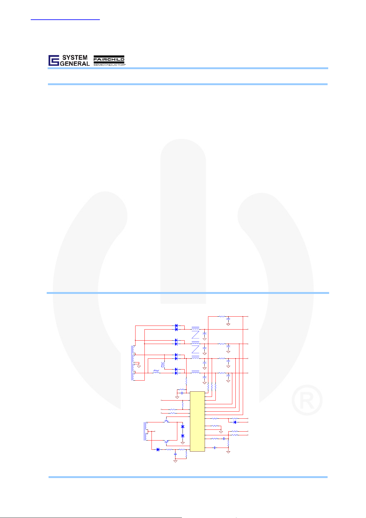
Main Transfor mer
5Vsb
Pok
Pson
Vdd
12V
5V
-5V
-12V
3.3V
5V
12V
12V
-12V
UVAC IS12
Vcc
PG
IS5
IS33
V33
V5
V12
VS12B
Pson
OP1
NVP
RI
GND
IN
COMP
SS
OP2
OPP
SG6108
FEATURES
PC half-bridge (or 494) power supply supervisor +
PWM
Highly Integrated and Few external components
required
Over voltage protection 3.3V/5V/12V (two 12V)
Under voltage protection 3.3V/5V/12V (two 12V)
Under voltage protection for –12V and/or –5V
Over current protection 3.3V/5V/12V (two 12V)
Over power protection
Short circuit protection
Power-down warning circuitry
Power good circuitry
Delay time for PSON and PG signals
Remote ON/OFF function
On-Chip oscillator and Error amplifier
Latching PWM for cycle-by-cycle switching
Soft-start
Maximum 48% duty cycle
APPLICATIONS
Switching mode power supplies for computers such
as ATX, NLX, and SFX (micro-ATX).
DESCRIPTION
The SG6108 controller is designed for desktop PC
switching mode power supplies. It provides everything
necessary to monitor and control the output of the power
supply. Remote ON/OFF control, power good circuitry,
over-voltage protection, over-power protection, and
over-current protection are all included. The SG6108
directly senses all the output rails for over voltage
conditions without requiring external dividers. An
innovative AC-signal sampling circuit provides an
adequate power-down warning signal for PG. A built-in
timer generates accurate timing for the control circuit.
Cycle-by-cycle PWM switching protects the power
transformer from saturation and ensures a rapid response
for short-circuit protection. This greatly reduces the stress
on the power transistors. The SG6108 utilizes a minimum
number of external components while including all the
functions needed for push-pull and/or half-bridge
topologies. This decreases production costs and PCB
space while increasing the power supply’s MTBF.
TYPICAL APPLICATION
查询SG6108DZ供应商
Page 2

Product Specification
Power Supply Supervisor + PWM SG6108
© System General Corp. - 2 - www.sg.com.tw • www.fairchildsemi.com
Version 1.0.1 (IAO33.0048.B0) September 26, 2007
1
2
3
4
5
6
7
8
9
10
20
19
18
17
16
15
14
13
12
11
PSON
V33
V5
OPP
UVAC
NVP
VS12
OP2
OP1
PG
VS12B
IS12
IS5
IS33
GND
COMP
IN
SS
RI
VCC
MARKING DIAGRAMS P I N CONFIGURATION
ORDERING INFORMATION
Part Number Pb-Free Package
SG6108DZ
20-Pin DIP
T : D = DIP
P : Z = Lead Free
Null=regular package
XXXXXXXX: Wafer Lot
Y: Year; WW: Week
V: Assembly Location
20
1
SG6
108
TP
XXXXXXXXYWWV
Page 3

Product Specification
Power Supply Supervisor + PWM SG6108
© System General Corp. - 3 - www.sg.com.tw • www.fairchildsemi.com
Version 1.0.1 (IAO33.0048.B0) September 26, 2007
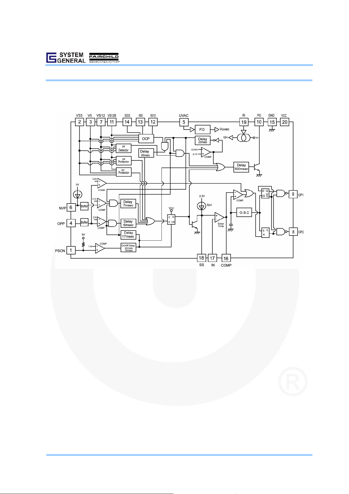
PIN DESCRIPTIONS
Name Pin Type Function
PSON 1 Logic Input
Remote On/Off logic input for the CPU or the controller. Turns the PWM output on/off following a 45
msec / 16 msec delay.
PSON = 0 means that the main SMPS is operational.
PSON =1 means that the main SMPS is off and the latch is reset.
V33 2 Analog Input 3.3V over-voltage/under-voltage control sense input.
V5 3 Analog Input 5V over-voltage/under-voltage control sense input.
OPP 4 Analog Input
Over-power sense input. This pin is connected to the driver transformer or the output of the current
transformer. When not in use, this pin should be grounded.
UVAC 5 Analog Input AC fail-detection. This detects main AC voltage under-voltage and/or failure.
NVP 6 Analog Input The protection input for negative outputs, such as –12V and/or –5V. Trip voltage = 2.1V.
VS12 7 Analog Input 12V over-voltage/under-voltage control sense input.
OP2/OP1 8/9 Analog Output
The totem-pole output drivers of a push-pull PWM. The outputs are enabled (low) only when the
NAND gate inputs are high. The maximum duty cycle on an output (OP1 or OP2) is 48%.
PG 10 Logic Output
Power Good logic output, 0 or 1 (open-collector). PG = 1 means that the power is good for operation.
The PG delay is 300 msec.
VS12B 11 Analog Input Second 12V over-voltage/under-voltage control sense input.
IS12 12 Analog Input 12V over current protection sense input. The sink current = 8 x IRI
IS5 13 Analog Input 5V over current protection sense input. The sink current = 8 x IRI
IS33 14 Analog Input 3.3V over current protection sense input. The sink current = 8 x IRI
GND 15 Supply Ground.
COMP 16 Analog Output The error amplifier output and the input of the PWM comparator.
IN 17 Analog Input
The negative input of the error amplifier. The positive input of the error amplifier is a 2.5V reference
voltage.
SS 18 Analog Input
Soft-start. This can be set through the external capacitor. The current source output at this pin is 8uA
and the voltage is clamped at 2.5V.
RI 19
Program.
Analog Input
This is connected to the external resistor to provide a reference setting. It determines the PWM
frequency, and also the OCP current setting. Setting RI = 75kΩ will result in a PWM frequency of
65kHz. Do not attach a capacitor to this pin. For OCP current settings please refer to the Over Current
Protection section on page 13.
VCC 20 Supply Supply voltage. 4.5V ~ 5.5V. It is connected to the 5V-standby.
Page 4
Product Specification
Power Supply Supervisor + PWM SG6108
© System General Corp. - 4 - www.sg.com.tw • www.fairchildsemi.com
Version 1.0.1 (IAO33.0048.B0) September 26, 2007
BLOCK DIAGRAM
Page 5
Product Specification
Power Supply Supervisor + PWM SG6108
© System General Corp. - 5 - www.sg.com.tw • www.fairchildsemi.com
Version 1.0.1 (IAO33.0048.B0) September 26, 2007
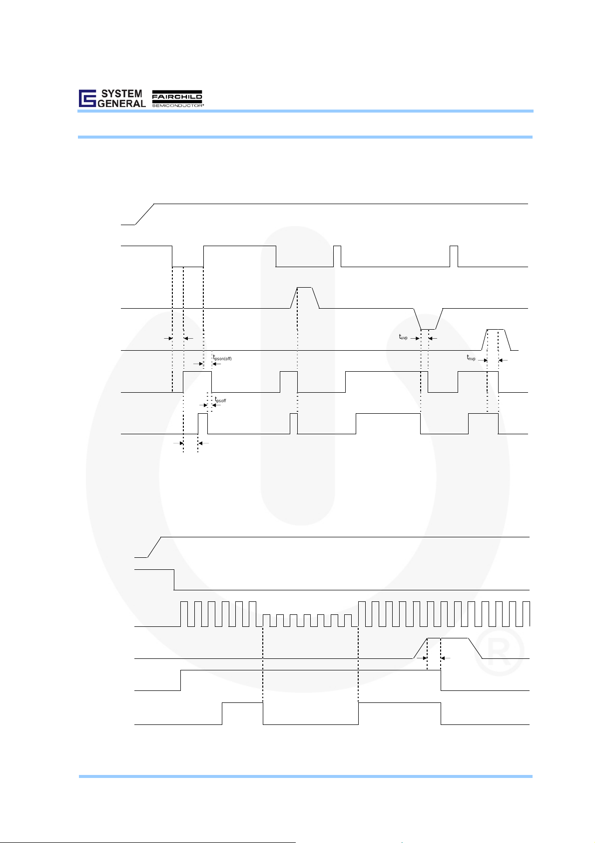
TIMING DIAGRAM
VCC
PSON
3.3V,5V,12V
t
pson(on)
t
uvp
NVP
t
pson(off)
t
nvp
SS(on/off)
t
psoff
PG
t
PG
VCC
PSON
Voltage < V
UVAC
UVAC
t
OPP
OPP
SS(on/off)
PG
Page 6

Product Specification
Power Supply Supervisor + PWM SG6108
© System General Corp. - 6 - www.sg.com.tw • www.fairchildsemi.com
Version 1.0.1 (IAO33.0048.B0) September 26, 2007
ABSOLUTE MAXIMUM RATINGS
Symbol Parameter Value Unit
V
CC, MAX
DC Supply Voltage at Pin 20 6 V
I
OUT
Input Current at PG,FB Pins 30 mA
OP1, OP2, VS12, VS12B, IS12 -0.3 to 16 V V
PIN, MAX
OPP, UVAC, RI, SS, PG, IN, COMP, FB, NVP, IS5, V33, V5, PSON -0.3 to 7 V
P
D,25
℃
Power Dissipation (TA=25℃) 1.5 W
P
D,90
℃
Power Dissipation (TA=90℃) 0.5 W
T
STG
Storage Temperature Range -55 to +150 ℃
R
θJA
Thermal Resistance, Junction-To-Case 28.58 ℃/W
T
J,MAX
Operating Junction Temperature 150 ℃
T
A,MAX
Operating Ambient Temperature -20 to +85 ℃
T
L
Lead Temperature (Wave soldering or IR, 10seconds) 260 ℃
ESD Capability, HBM model 3.0 KV
ESD Capability, Machine model 200 V
* All voltage values, except the differential voltage, are given with respect to the network ground terminal.
* Stresses beyond those listed under “absolute maximum ratings” may cause permanent damage to the device.
RECOMMENDE D OPERA TIN G COND ITION S
Symbol Parameter Value Unit
V
CC
DC Supply Voltage 4.5 to 5.5 V
TA Operating Ambient Temperature -20 to +85 ℃
* For proper operation
Electrical Characteristics (VCC=5V, TA = 25°C,RI=75Kohm,unless noted)
VCC Section
Symbol Parameter Test Condition Min. Typ. Max. Unit
I
CC1
Total Supply Current PSON=Low,
OP1/OP2 1000pF
10 mA
I
CC2
Total Supply Current PSON=High,
OP1/OP2 1000pF
5 10 mA
Page 7

Product Specification
Power Supply Supervisor + PWM SG6108
© System General Corp. - 7 - www.sg.com.tw • www.fairchildsemi.com
Version 1.0.1 (IAO33.0048.B0) September 26, 2007
Protection Section
Symbol Parameter Test Condition Min. Typ. Max. Unit
V
OVP1
Over-Voltage Protection 3.3V 3.9 4.1 4.3 V
V
OVP2
Over-Voltage Protection 5V 5.8 6.1 6.5 V
V
OVP3
Over-Voltage Protection VS12,VS12B 13.75 14.05 14.35 V
V
UVP1
Under-Voltage Protection 3.3V 2.0 2.6 2.8 V
V
UVP2
Under-Voltage Protection 5V 3.0 3.6 3.9 V
V
UVP3
Under-Voltage Protection VS12,VS12B 6.0 7.2 8.0 V
V
UVS1
Under-Voltage Sense 3.3V for PG Low 2.5 2.8 3.0 V
V
UVS2
Under-Voltage Sense 5V for PG Low 4.0 4.3 4.5 V
V
UVS3
Under-Voltage Sense VS12,VS12B for PG Low 9.4 10.1 10.4 V
V
OPP
* 1 Over-Power Protection (With T
OPP
delay time) V
UVAC
= 1.5V 2.23 2.3 2.37 V
V
OPPH
Over-Power Protection (Without delay time) 3.0 3.2 3.4 V
VX
Disable Under Voltage / Over Power Protection
threshold
0.2 0.3 0.4 V
V
NVP
Negative Voltage Protection: Voltage Level 2.0 2.1 2.2 V
I
NVP
Negative Voltage Protection: Source Current 57 64 72 uA
T
UVEDA
Under Voltage Enable Delay Time VS12/B = 0.8V 10 17 22 mS
T
UVEDB
Under Voltage Enable Delay Time VS12/B = 5V 22 30 40 mS
T
OVP
Timing for Over-Voltage Protection 0.37 0.7 1.35 mS
T
UVP
Timing for Under-Voltage Protection 1.2 2.7 4.2 mS
T
UVS
Timing for Under-Voltage Sense (PG Low) 0.9 1.6 2.2 mS
T
OPP
Timing for Over-Power-Protection 4 6 8 mS
T
NVP
Timing for Negative Voltage Protection 3.3 7 10.2 mS
T
OCP
Timing for Over-Current Protection 15 20 25 mS
SS go Hi, VS12/B=0.8V
10 17 22
T
OCP(EN)
Timing for Over-Current Protection Function Enable
SS go Hi, VS12/B =5V 22 30 40
mS
V
OFFSET
OCP Comparator Input Offset Voltage -5 5 mV
I
REF
Ratio of IS33, IS5, IS12 to RI Current Setting 7.6 8 8.4
I
LK33
V33 Leakage Current V33 = 3.3V 50 uA
I
LK5
V5 Leakage Current V5= 5V 50 uA
I
LK12AB
VS12, VS12B Leakage Current
VS12 =12V
VS12B = 12V
50 uA
Note *1: V
OPP
= (2/3) x V
OPP
+ (1/3) x V
UVAC
;
Power Good Section
Symbol Parameter Test Condition Min. Typ. Max. Unit
TPG Timing for PG Delay 200 300 400 mS
T
UVAC
Timing for PG Fail UVAC to PG 75 150 300 uS
V
UVAC
UVAC Voltage Sense for PG 0.68 0.7 0.72 V
V
UVAC(DIS)
Disable UVP,NVP,OCP Voltage 0.68 0.7 0.72 V
T
UVAC(DIS)
Timing for Disable UVP,NVP,OCP UVAC < V
UVAC(DIS)
75 150 300 uS
T
UVAC(EN)
Timing for Enable UVP,NVP,OCP UVAC > V
UVAC(DIS)
15 25 35 mS
T
R
*2
PG Output Rising Time
CL =100pF Pull 2.2K to
5V
1 3 uS
T
F
*2
PG Falling Time
CL =100pF Pull 2.2K to
5V
300 500 nS
V
OL2
Power Good Output Saturation Level IPG = 5mA 0.5 V
I
IO2
Power Good Leakage Current VPG = 5V 1 uA
Note *2: Not tested in production test;
Page 8

Product Specification
Power Supply Supervisor + PWM SG6108
© System General Corp. - 8 - www.sg.com.tw • www.fairchildsemi.com
Version 1.0.1 (IAO33.0048.B0) September 26, 2007
Remote On/Off
Symbol Parameter Test Condition Min. Typ. Max. Unit
V
PSON
PSON Input Threshold Level 1 1.4 2.0 V
I
PSON
Remote Input Driving Current 0.5 mA
T
PSON(ON)
T
PSON(OFF)
PSON to On/Off Time
On
Off
25
8
45
16
65
24
mS
T
PSOFF
PG Low to Power Off Time 1.5 2 6.3 mS
Error Amplifier
Symbol Parameter Test Condition Min. Typ. Max. Unit
V
2.5
Reference Voltage 2.45 2.5 2.55 V
I
IB
*2
Input Bias Current 0.1 uA
V
DEV,T2.5
*2
Deviation of V
2.5
Over Temperature 10 30 mV
I
COSI
I
COMP
Source Current IN Short COMP
VCOMP=2.4V
0.4 mA
I
COSO
I
COMP
Sink Current IN Short COMP
VCOMP=2.6V
1.2 mA
A
VOL
* 2
Open-Loop Voltage Gain 50 60 dB
BW
* 2
Unity Gain Bandwidth 0.3 1 MHz
PSRR
* 2
Power Supply Rejection Ratio 50 dB
Oscillator Section
Symbol Parameter Test Condition Min. Typ. Max. Unit
F
OSC
PWM Frequency 60 65 70 KHz
DC
MAX
Max Duty Cycle 41 44.5 48 %
RI RI Resistor Range 70 105 KΩ
V
REFRI
RI Reference Voltage 0.98 1 1.02 V
T
DEAD
PWM Dead Time 1.3 1.7 2.1 uS
Soft-Start Section
Symbol Parameter Test Condition Min. Typ. Max. Unit
ISS Charge Current 6.7 8 9.3 uA
I
SSINK
Sink Current 1 mA
PWM Output Section (OP1, OP2)
Symbol Parameter Test Condition Min. Typ. Max. Unit
VOL Output Voltage Low Io = 20mA 1 V
VOH Output Voltage High VDD = 5V 4 V
RO Output Impedance of VOH 0.8 2.6 kΩ
Page 9

Product Specification
Power Supply Supervisor + PWM SG6108
© System General Corp. - 9 - www.sg.com.tw • www.fairchildsemi.com
Version 1.0.1 (IAO33.0048.B0) September 26, 2007
TYPICAL CHARACTERISTICS
Total Supply Current (I
CC1
) vs Tem perature
0
3
5
8
10
13
15
-40 -25 -10 5 20 35 50 65 80 95 110 125
Temperature (℃)
I
CC1
(mA )
Over-Power Protection (With TOPP delay time)
(V
OPP
* 1) vs Temperature
2.23
2.25
2.27
2.29
2.31
2.33
2.35
2.37
-40 -25 -10 5 20 35 50 6 5 80 95 1 10 125
Temperature (℃)
V
OPP
*
1
(V)
Over P ower Protection (Without delay time) (V
OPPH
)
vs Temperature
3.0
3.1
3.2
3.3
3.4
-40 -25 -10 5 20 35 50 65 80 95 110 125
Temperature (℃)
V
OPPH
(V)
Negative Voltage Protection: Voltage Level (V
NVP
) vs
Temperature
1.0
1.5
2.0
2.5
3.0
3.5
-40 -25 -10 5 20 35 50 65 80 95 110 125
Temperature (℃)
V
NVP
(V)
Negative Voltage Protec tion: Source Current (I
NVP
)
vs Temperature
64
65
66
67
68
69
-40 -25 -10 5 20 35 50 65 80 95 110 125
Temperature (℃ )
I
NVP
(uA)
Timing for Over-Power-Protection
(T
OPP
) vs Temperature
4.0
4.5
5.0
5.5
6.0
6.5
7.0
7.5
8.0
-40 -25 -10 5 20 35 50 65 80 95 110 125
Temperature (℃)
T
OPP
(
mS)
Page 10

Product Specification
Power Supply Supervisor + PWM SG6108
© System General Corp. - 10 - www.sg.com.tw • www.fairchildsemi.com
Version 1.0.1 (IAO33.0048.B0) September 26, 2007
Timing for Ov er-Current Protection (T
OCP
) vs
Temperature
15
17
19
21
23
25
-40 -25 -10 5 20 35 50 65 80 95 110 125
Temperature (℃ )
T
OCP
(mS)
OCP Com parator Input Offset Voltage (V
OFFSET
) vs
Temperature
-5.0
-3.0
-1.0
1.0
3.0
5.0
-40 -25 -10 5 20 35 50 65 80 95 110 125
Temperature (℃)
V
OFFSET
(mV)
Ratio of IS12 to R I Curren t Setting ( I
REF
) vs
Temperature
7.7
7.8
7.9
8.0
8.1
8.2
8.3
8.4
-40 -25 -10 5 20 35 5 0 65 80 95 110 12 5
Temperature (℃ )
I
REF
VS12 Leakage Current (I
LK12AB
_VS12 ) vs
Temperature
15
16
17
18
19
20
-40 -25 -10 5 20 35 50 65 80 95 1 10 125
Temperature (℃)
I
LK12AB
_VS12 (uA)
VS12B Leak age Current ( I
LK12AB
_VS12B) vs
Temperature
15
16
17
18
19
20
-40 -25 -10 5 20 35 50 65 80 95 110 125
Temperature (℃)
I
LK12AB
_VS12B (uA)
UVAC Volta ge Se nse fo r PG ( V
UVAC
) vs Temperature
0.68
0.69
0.70
0.71
0.72
-40 -25 -10 5 20 35 50 65 80 95 11 0 1 25
Temperature (℃)
V
UVAC
(V)
Page 11

Product Specification
Power Supply Supervisor + PWM SG6108
© System General Corp. - 11 - www.sg.com.tw • www.fairchildsemi.com
Version 1.0.1 (IAO33.0048.B0) September 26, 2007
Reference Voltage (V
2.5
) vs Temper ature
2.45
2.47
2.49
2.51
2.53
2.55
-40 -25 -10 5 20 35 50 65 80 95 110 125
Temperature (℃)
V
2.5
(V)
PWM Frequency (F
OSC
) vs Temperature
60
62
64
66
68
70
-40 -25 -10 5 20 35 50 65 80 95 110 125
Temp erature (℃ )
F
OSC
(KHz )
Max Duty Cycle (DC
MAX
) vs Temperature
42
43
44
45
46
47
-40 -25 -10 5 20 35 50 65 80 95 110 125
Temperature (℃)
DC
MAX
(%)
RI Reference Voltage (V
REFRI
) vs Tempera ture
0.98
0.99
1.00
1.01
1.02
-40 -25 -10 5 20 35 50 65 80 95 110 125
Temperature (℃)
V
REFRI
(V)
PWM Dead Time (T
DEAD
) vs Temperature
1.3
1.4
1.5
1.6
1.7
1.8
-40 -25 -10 5 20 35 50 65 80 95 110 125
Temperature (℃)
T
DEAD
(uS)
Charge C urrent (ISS) vs Temperature
7.4
7.6
7.8
8.0
8.2
8.4
8.6
-40 -25 -10 5 20 35 50 65 80 95 110 125
Temperature (℃)
I
SS
(uA)
Page 12

Product Specification
Power Supply Supervisor + PWM SG6108
© System General Corp. - 12 - www.sg.com.tw • www.fairchildsemi.com
Version 1.0.1 (IAO33.0048.B0) September 26, 2007
Operation description
Protection against over-voltage, short-circuit and fault
conditions is mandatory for PC power supplies. Many
commonly used protection circuits require large numbers
of discrete components and comparators which occupy
significant PCB space and add to assembly costs. This
single chip controller IC provides complete protection,
shunt regulation, and PWM control with comparatively
few components. The SG6108 is an ideal controller IC for
PC switching mode power supplies. The features and
benefits of this device are listed on the first page.
Feature Notes
Over voltage protection can be implemented without
any additional components. Over-voltage sense
levels are 3.3V/5V/12V or 4.1V/6.1V/14.05V.
The SG6108’s over current protection monitors the
3.3V, 5V, and the two 12V levels. The voltage
difference across the external current shunt is used to
provide accurate OCP.
Over current and/or short circuit protection can also
be implemented by using over-power protection. To
do this, the OPP pin must be connected to the current
transformer (driver transformer).
The power good signal is asserted to indicate that the
3.3V/5V/12V signals are above the under voltage
threshold level. The PG pin goes high when the
above condition is reached. A 2kΩ pull up resistor
may be optionally connected to the 5V lead.
VCC can be supplied from the 5V-standby.
Whenever the VCC voltage exceeds 7V the entire
SG6108 will be shutdown and reset (except for the
shunt regulator). No extra power supply is needed.
Complete PWM control circuitry includes an error
amplifier for push-pull or half-bridge operation.
Supervisory Circuit Operation
The PC generates the remote ON/OFF logic (PSON)
signal. When this is “Low” the power supply is “On”.
When it is “High”, the power supply is switched off. The
remote ON/OFF signal is supplied to the PSON input.
Application Guides
The application guide shows the key features of the
SG6108 and illustrates how to use it in an ATX switching
mode power supply (SMPS). The SG6108 is suitable for
half-bridge, push-pull topologies. The PWM section of
the SG6108 comprises a built-in 65kHz oscillator and
high immunity circuits, which protect the system from
noise interference and provide higher noise margins
against improper PCB layout. The SG6108 has OVP,
UVP, and OCP for the 3.3V and 5V signals, as wells as
both 12V signals. NVP is used for negative voltage
protection (–12V/–5V). UVAC (AC failure detection) is
used to measure the AC line voltage.
AC Failure Detection
UVAC is connected to the secondary power transformer
through a resistor divider. UVAC is used for detecting the
AC line voltage. Whenever the UVAC voltage drops
below 0.7V for a period of time such as 150usec, the PG
(power good) signal will be pulled low to indicate an AC
line power-down condition.
The voltage amplitude of the PWM switching signal in the
secondary power transformer is proportional to the AC
line voltage. The power-down warning threshold can be
controlled by adjusting the resistor-divider ratio. A small
capacitor must be connected between UVAC and ground
to filter the switching noise.
Over Power Protection (OPP)
OPP (over power protection) is used to detect over power
and short-circuit conditions. Whenever the V
OPP
voltage
(p.7, Note-1) exceeds 2.3V for longer than 6msec the
SG6108 will pull PG low and lock off the power outputs.
+
UVAC
Vo
0.7V
R1
R2 C1
VS
Vin
Page 13

Product Specification
Power Supply Supervisor + PWM SG6108
© System General Corp. - 13 - www.sg.com.tw • www.fairchildsemi.com
Version 1.0.1 (IAO33.0048.B0) September 26, 2007
+
R2R1
2.1V
64uA
-12V
-5V
Vdd
OPP
OP2
OP1
R1 R2
R3
C1
Over Current Protection (OCP)
The SG6108 provides over current protection for the
3.3V, 5V and the two 12V rails. Whenever an OCP
condition occurs at any of the voltage rails, PG will be low
and PWM will be turned off. The internal OCP
comparators have a very small offset voltage (±5mV).
The sink currents of IS33, IS5, and IS12 are 8 times the
current at the RI pin. The current at the RI pin is V
RI
/RI.
Here is an example demonstrating how to set the over
current protection threshold:
I
RI
= VRI/RI = 1.0V/75k = 13.3uA
If R1 = 1700Ω and R12 = 0.01Ω, then
OC P = 13.3uA x 8 x 1700 / 0.01 = 18 A
Negative Voltage Protection
NVP provides UVP (under voltage protection) for
negative voltage outputs. An under-voltage condition
indicates an overload at a negative voltage output. For
example, the –12V output may drop to –10V during
overload situations. The resistance of a resistor connected
from NVP to the negative voltage output determines the
protection threshold voltage. NVP outputs a 64uA
constant current to the negative voltage output via this
resistor. Whenever the NVP voltage exceeds 2.1V for
longer than 7 msec the SG6108 will lock the power
outputs off.
VNVP = 64 uA × (R1 + R2) – V-12V
The power outputs will be locked off when VNVP ≥
2.1V.
Page 14

Product Specification
Power Supply Supervisor + PWM SG6108
© System General Corp. - 14 - www.sg.com.tw • www.fairchildsemi.com
Version 1.0.1 (IAO33.0048.B0) September 26, 2007
REFERENCE CIRCUIT
Page 15

Product Specification
Power Supply Supervisor + PWM SG6108
© System General Corp. - 15 - www.sg.com.tw • www.fairchildsemi.com
Version 1.0.1 (IAO33.0048.B0) September 26, 2007
PACKAGE INFORMATION
20 PINS – DIP (D)
θ
e
B
E
A
A2
e
A1
L
b
b1
10
1
D
20
11
E1
Dimensions
Millimeters Inches
Symbol
Min. T
yp
.Max.Min.T
yp
.Max.
A 5.334 0.210
A1 0.381 0.015
A2 3.175 3.302 3.429 0.125 0.130 0.135
b
1.524 0.060
b
1 0.457 0.018
D 24.892 26.162 26.924 0.980 1.030 1.060
E 7.620 0.300
E1 6.223 6.350 6.477 0.245 0.250 0.255
e 2.540 0.100
L 2.921 3.302 3.810 0.115 0.130 0.150
eB 8.509 9.017 9.525 0.335 0.355 0.375
θ˚ 0° 7° 15° 0° 7° 15°
Page 16

Product Specification
Power Supply Supervisor + PWM SG6108
© System General Corp. - 16 - www.sg.com.tw • www.fairchildsemi.com
Version 1.0.1 (IAO33.0048.B0) September 26, 2007
 Loading...