

Page 1

Product Specification
Power Supply Supervisor + Regulator + PWM
SG6105A
© System General Corp. - 1 - www.sg.com.tw • www.fairchildsemi.com
Version 1.0.1 (IAO33.0072.B0) September 25, 2007
FEATURES
PC half-bridge (or 494) power supply supervisor +
two 431 + PWM
High integration & few external components
Over-voltage protection for 3.3V, 5V, and 12V
Under-voltage protection for 3.3 V , 5V, and 12V
Under-voltage protection for –12V and/or –5V
Over-power and short-circuit protection
Power-down warning circuitry
Power-good circuitry
Delay time for PSON and PG signal
Remote ON/OFF function
On-chi p oscillator and error a mplifier
Two shunt regulators for 3.3V and 5V-standby
Latching PWM for cycle-by-cycle switching
Push-pull PWM operation and totem pole outputs
Soft-start and maximum 93% duty cycle
APPLICATIONS
Switching mode power supply for computers:
AT
NLX
SFX (mi c ro-ATX)
DESCRIPTION
SG6105A controller is designed for switching-mode
power supplies for desktop PCs. It provides all the
functi ons ne cessa ry to m onit or and con trol the outp ut
of the power supply. Remote ON/OFF control,
power–good circuitry, and protection features against
over-voltage and over-power are implemented. It
directly senses all the output rails for OVP without
the need for external dividers. An innovative
AC-signal sampling circuitry provides a sufficient
power-down warning signal for PG.
A built-in timer generates accurate timing for the
control circuit, including the PS-off delay. The
cycle-by-cycle PWM switching prevents the power
transformer from saturation and ensures the fastest
response for the short-circuit protection, which
greatly reduces stress for power transistors. Two
internal precision TL431 shunt regulators provide
stable reference voltage and a driver for 3.3V and 5V
standby regulation.
Utilizing minimum external components, the
SG6105A includes the functions for push-pull and/or
half-bridge topology, decreasing production c ost and
PCB space, and increasing the MTBF for power
supply.
查询SG6105A供应商
Page 2
Product Specification
Power Supply Supervisor + Regulator + PWM
SG6105A
© System General Corp. - 2 - www.sg.com.tw • www.fairchildsemi.com
Version 1.0.1 (IAO33.0072.B0) September 25, 2007
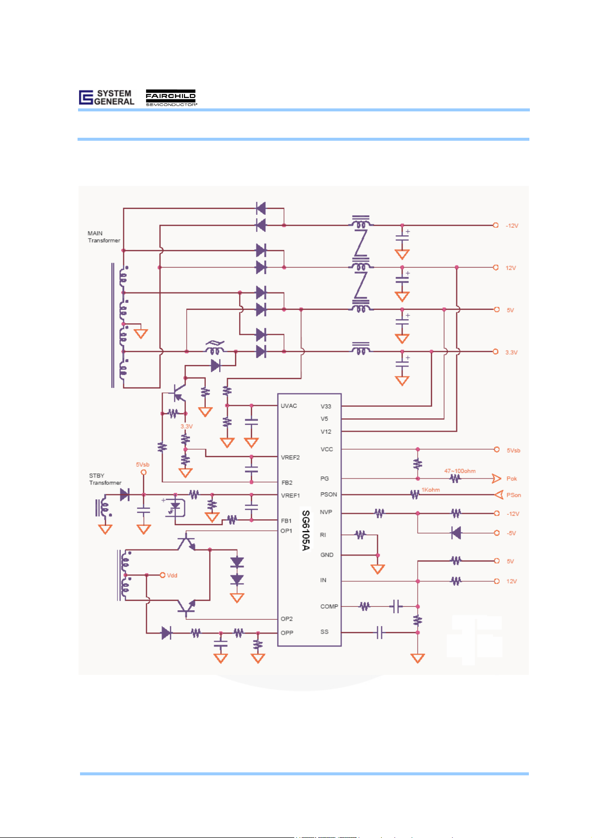
TYPICAL APPLICATION 1
Page 3
Product Specification
Power Supply Supervisor + Regulator + PWM
SG6105A
© System General Corp. - 3 - www.sg.com.tw • www.fairchildsemi.com
Version 1.0.1 (IAO33.0072.B0) September 25, 2007
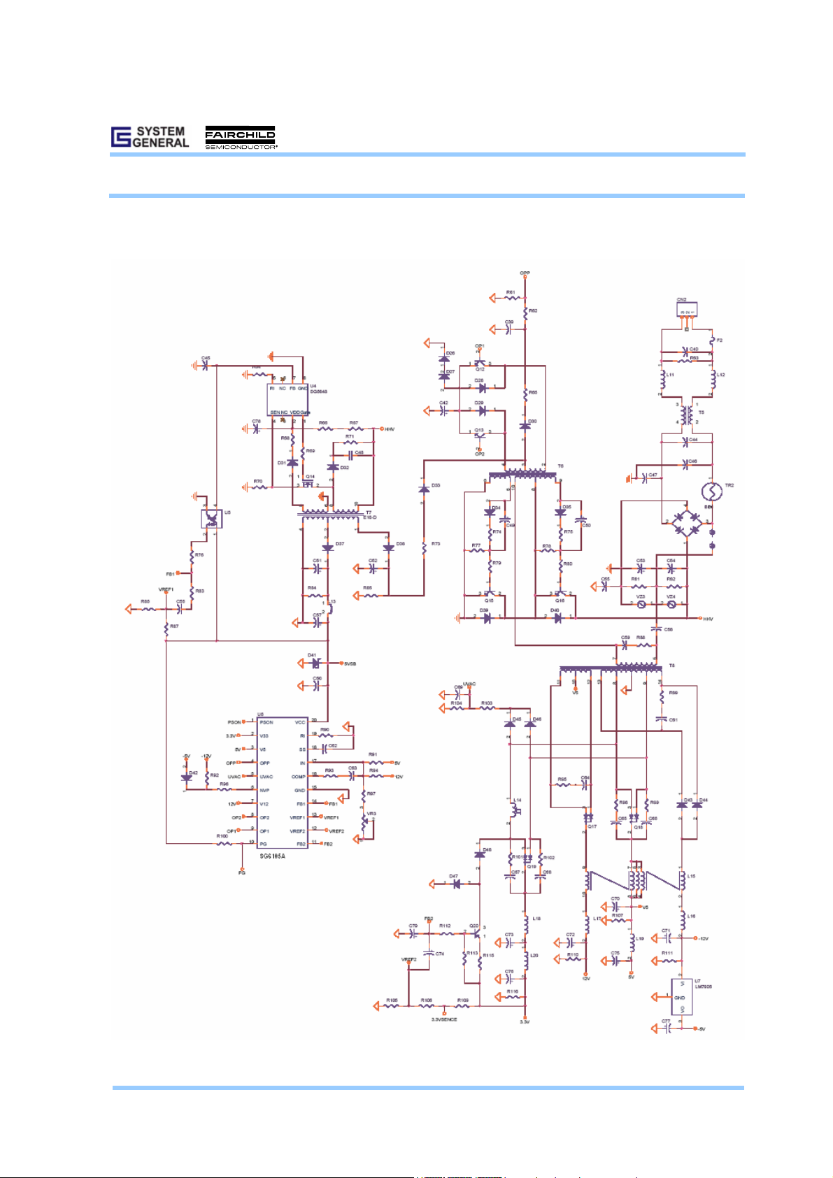
TYPICAL APPLICATION 2
Page 4
Product Specification
Power Supply Supervisor + Regulator + PWM
SG6105A
© System General Corp. - 4 - www.sg.com.tw • www.fairchildsemi.com
Version 1.0.1 (IAO33.0072.B0) September 25, 2007
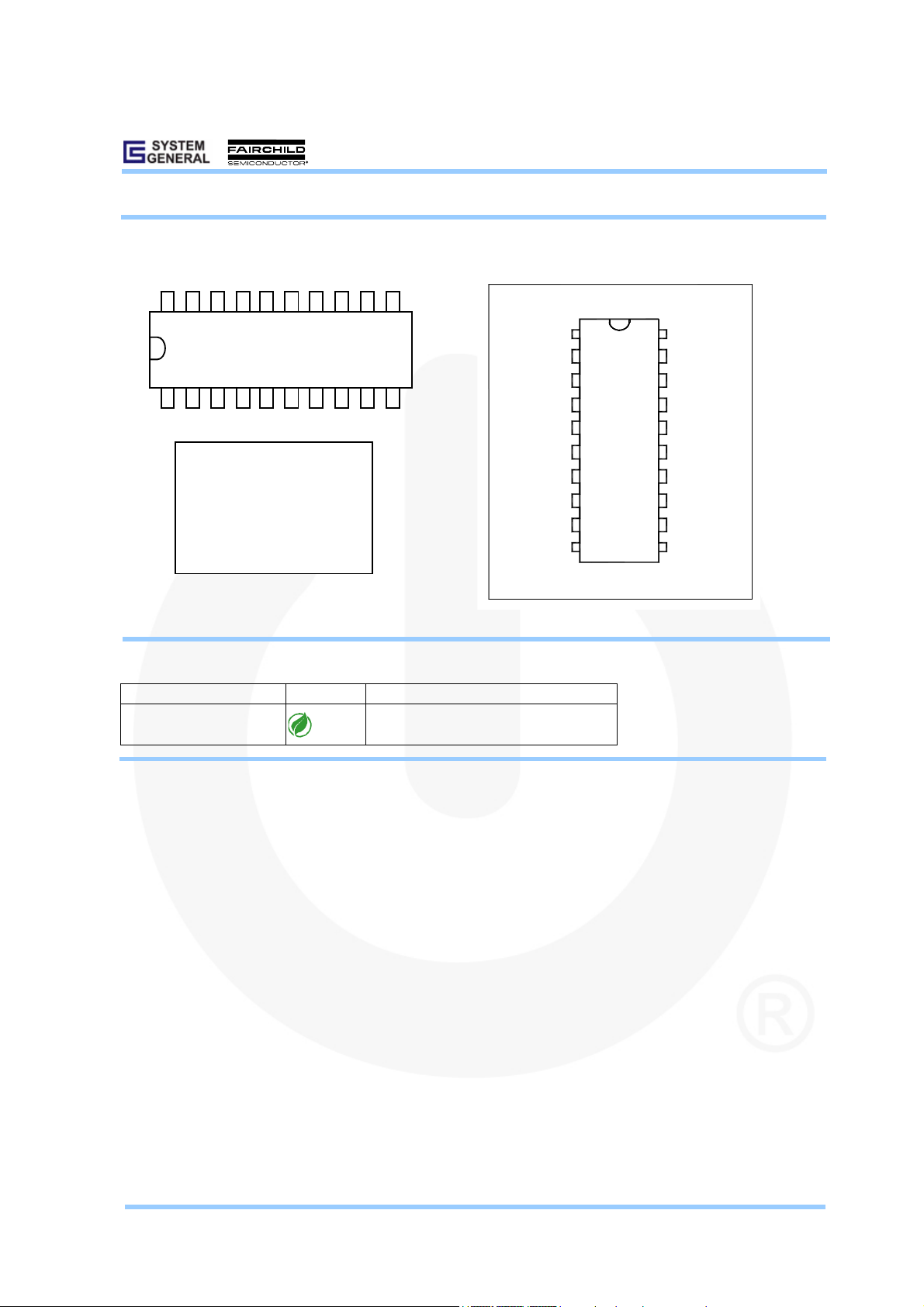
MARKING DIAGRAMS PIN CONFIGURATION
ORDERING INFORMATION
Part Number Pb-Free Package
SG6105ADZ
20-Pin DIP
20
1
SG6105ATP
XXXXXXXXYWWV
1
2
3
4
5
6
7
8
9
10
20
19
18
17
16
15
14
13
12
11
PSON
V33
V5
OPP
UVAC
NVP
V12
OP2
OP1
PG
FB2
VREF2
VREF1
FB1
GND
COMP
IN
SS
RI
VCC
T : D = DIP
P : Z = Lead Free
Null=regular package
XXXXXXXX: Wafer Lot
Y: Year; WW: Week
V: Assembly Location
Page 5
Product Specification
Power Supply Supervisor + Regulator + PWM
SG6105A
© System General Corp. - 5 - www.sg.com.tw • www.fairchildsemi.com
Version 1.0.1 (IAO33.0072.B0) September 25, 2007
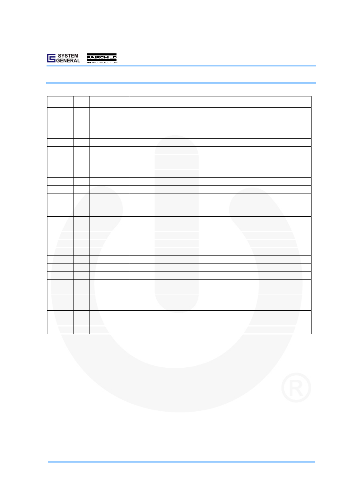
PIN DESCRIPTIONS
Name Pin Type Function
PSON 1 Logic Input
Remote on/off logic input for CPU or controller. Turn on/off the PWM output after the 7.5ms
/ 26ms delay.
PSON = 0, the main SMPS is operational.
PSON =1, the main SMPS is off and the latch is reset.
V33 2 Analog Input 3.3V over-voltage/under-voltage control sense input.
V5 3 Analog Input 5V over-voltage/under-voltage control sense input.
OPP 4 Analog Input
Over-power sense input. This pin is connected to driver transformer or the Output of current
transformer. When not in use, this pin should be grounded.
UVAC 5 Analog Input AC fail detection, detect main AC voltage under-voltage and/or failure.
NVP 6 Analog Input The protection input for negative Output, such as –12V and/or –5V. Trip voltage = 2.1V.
V12 7 Analog Input 12V over-voltage/under-voltage control sense input.
OP1/OP2 9/8 Analog Output
The totem-pole Output drivers of push-pull PWM. The Output are enabled (low) only when
the NAND gate inputs are high. The maximum duty cycle on an Output (OP1 or OP2) is
46%.
PG 10 Logic Output
Power-good logic output, 0 or 1 (open-collector). PG = 1, the power is good for operation.
The PG delay is 300ms.
FB2 11 Analog Output Output for second converter regulation loop.
VREF2 12 Analog Input Reference comparison input for second converter regulation loop, 2.5V.
VREF1 13 Analog Input Reference comparison input for first converter regulation loop, 2.5V.
FB1 14 Analog Output Output for first converter regulation loop.
GND 15 Supply Ground.
COMP 16 Analog Output Error amplifier Output and the input of the PWM comparator.
IN 17 Analog Input
The negative input of error amplifier. The positive input of error amplifier is a 2.5V reference
voltage.
SS 18 Analog Input
The soft-start, settable through an external capacitor. The current source output at this pin
is 8µA and the voltage is clamped at 2.5V.
RI 19
Program Analog
Input
Connected to external resistor for the reference setting. R
I
= 75kΩ.
VCC 20 Supply Supply voltage. 4.5V ~ 5.5V connected to 5V-standby.
Page 6
Product Specification
Power Supply Supervisor + Regulator + PWM
SG6105A
© System General Corp. - 6 - www.sg.com.tw • www.fairchildsemi.com
Version 1.0.1 (IAO33.0072.B0) September 25, 2007
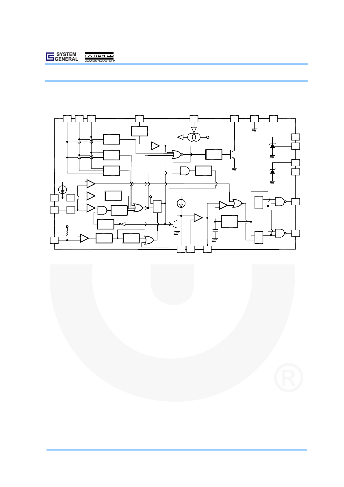
BLOCK DIAGRAM
SS
2.5V
8uA
Vcc
NVP
+
6
Delay
7msec
Buffer
2.1V
3.2V
V33
V5
2 3
5V
64uA
UVAC
V12
7
5
UV
Detector
OV
Protector
UV
Protector
COMP
_
COMP
+
_
COMP
_
DSD
0.7V
+
2uA
2.4V
OPP
4
Buffer
Vcc
PSON
1
+
1.4V
_
Delay
2msec
Delay
15msec
COMP
_
+
Delay
7msec
On/Off Delay
26msec
7.5msec
COMP
Q
D
CK
R
18
OP1
PG
10
RI
19
GND
15
20
VCC
Delay
300msec
Vref
Delay
3sec
FB2
11
VREF1 13
FB1
14
VREF2
12
+
Error
Amp
_
COMP
_
+
O.S.C
COMP
16 17
IN
Q
_
CK
D
Q
R
SQ
OP2
8
9
Page 7

Product Specification
Power Supply Supervisor + Regulator + PWM
SG6105A
© System General Corp. - 7 - www.sg.com.tw • www.fairchildsemi.com
Version 1.0.1 (IAO33.0072.B0) September 25, 2007
TIMING DIAGRAM
VCC
PSON
3.3V,5V,12V
t
PSON(ON)
t
UVP
NVP
t
PSON(OFF)
t
NVP
SS(on/off)
t
PSOFF
PG
t
PG
VCC
PSON
Voltage < V
UVAC
UVAC
OPP
t
OPP
SS(on/off)
PG
Page 8

Product Specification
Power Supply Supervisor + Regulator + PWM
SG6105A
© System General Corp. - 8 - www.sg.com.tw • www.fairchildsemi.com
Version 1.0.1 (IAO33.0072.B0) September 25, 2007
ABSOLUTE MAXIMUM RATINGS
Symbol Parameter Value Unit
VCC DC Supply Voltage at Pin 20 16 V
I
OUT
Output Current at PG, Fb1, Fb2 Pins 30 mA
V12, OP1, OP2, FB1, FB2, SS -0.3 to 16 V VPIN
PSON, V33, V5, VREF1, VREF2, OPP, UVAC, RI, NVP, IN, COMP, PG -0.3 to 7 V
P
D,25
℃
Power Dissipation (T
A
=25°C) 1.5 W
P
D,
90℃
Power Dissipation (T
A
=90°C) 0.5 W
T
STG
Storage Temperature Range -55 to +150 °C
R
θJA
Thermal Resistance, Junction-To-Air 82.5 °C /W
T
J,MAX
Operating Junction Temperature 150 °C
T
A,MAX
Operating Ambient Temperature -30 to +125 °C
T
L
Lead Temperature (Soldering, 10 Seconds) 260 °C
ESD Electrostatic Discharge Capability, Human Body Model 3.0 KV
* All voltage values, except differential voltages, are given with respect to GND pin.
* Stresses beyond those listed under "absolute maximum ratings" may cause permanent damage to the device.
RECOMMENDED OPERATING CONDITIONS
Symbol Parameter Test Condition Value Unit
V
CC
DC Supply Voltage 4.5 to 5.5 V
VFB Shunt Regulator Output Fb1, Fb2 Pins 4 to 16 V
TA Operating Ambient Temperature Range -25 to +85 °C
* For proper operat i on .
Page 9

Product Specification
Power Supply Supervisor + Regulator + PWM
SG6105A
© System General Corp. - 9 - www.sg.com.tw • www.fairchildsemi.com
Version 1.0.1 (IAO33.0072.B0) September 25, 2007
ELECTRICAL CHARACTERISTICS
Values are provided for 4.5V≦VCC≦5.5V, TA = -25°C~+85°C, RI = 75KΩ, unless noted.
Symbol Parameter Test Condition Min. Typ. Max. Unit
ICC Total Supply Current PG High 5 10 mA
V
OVP1
Over-Voltage Protection 3.3V 3.9 4.1 4.3 V
V
OVP2
Over-Voltage Protection 5V 5.8 6.1 6.5 V
V
OVP3
Over-Voltage Protection 12V 13.9 14.5 14.9 V
V
UVP1
Under-Voltage Protection 3.3V 2.0 2.6 2.8 V
V
UVP2
Under-Voltage Protection 5V 3.0 3.6 3.9 V
V
UVP3
Under-Voltage Protection 12V 6.0 7.2 8.0 V
V
UVS1
Under-Voltage Sense 3.3V for PG Low 2.5 2.8 3.0 V
V
UVS2
Under-Voltage Sense 5V for PG Low 4.0 4.3 4.5 V
V
UVS3
Under-Voltage Sense 12V for PG Low 9.4 10.1 10.4 V
V
OPP
(*)
Over-Power Protection (With T
OPP
Delay Time) V
UVAC
= 1.5V 2.25 2.32 2.39 V
V
OPPH
Over-Power Protection (Without Delay Time) 3.0 3.2 3.4 V
VX
Disable Under-Voltage / Over-Power
Protection Threshold
0.2 0.3 0.4 V
V
NVP
Negative Voltage Protection: Voltage Level 2.0 2.1 2.2 V
I
NVP
Negative Voltage Protection: Source Current 63 67 71 µA
T
OVP
Timing for Over-Voltage Protection
0.37 0.70 1.35 ms
T
UVP
Timing for Under-Voltage Protection
0.80 2.40 3.75 ms
T
UVS
Timing for Under-V oltage Sense for PG Low
0.37 1.20 1.88 ms
T
OPP
Timing for Over-Power Protection
5 7 9 ms
T
NVP
Timing for Negative Voltage Protection
3.3 7.0 10.2 ms
Note *: V
OPPS
= (2/3) x V
OPP
+ (1/3 ) x V
UVAC
.
Shunt Regulator Section Current
Symbol Parameter Test Condition Min. Typ. Max. Unit
V
REF
Reference Voltage
I
FB
= 0.5mA, TA = 25℃
2.475 2.500 2.525 V
V
DEV, I
(**)
Deviation of V
REF
Over FB Current IFB = 0.5mA to 10mA 20 mV
V
DEV, T
(**)
Deviation of V
REF
Over Temperature 10 30 mV
R
EGLI-FB
(**)
Line Regulation
4 ≦ V
FB
≦ 15V
1 mV/V
I
OUT-FB
**
Output Sinking Current Capability V
FB
= 2V 10 mA
Note **: Not tested in producti on.
Power-Good Section
Symbol Parameter Test Condition Min. Typ. Max. Unit
TPG Timing for PG Delay RI = 75kΩ 200 300 400 ms
V
UVAC
UVAC Voltage Sense for PG 0.68 0.70 0.72 V
T
R
(**)
Power -Good Output Rising Time C
L
= 100pF, Pull 2.2K to 5V 1 3 µs
T
F
(**)
Power-Good Falling Time C
L
= 100pF, Pull 2.2K to 5V 300 500 ns
V
OL2
Power-Good Output Saturation Level IPG = 5mA 0.5 V
I
ON2
Power-Good Leakage Current Collector VPG = 5V 1 µA
Note **: Not tested in producti on.
Page 10

Product Specification
Power Supply Supervisor + Regulator + PWM
SG6105A
© System General Corp. - 10 - www.sg.com.tw • www.fairchildsemi.com
Version 1.0.1 (IAO33.0072.B0) September 25, 2007
Remote On/Off Section
Symbol Parameter Test Condition Min. Typ. Max. Unit
VIH High-level Input Voltage 2 V
VIL Low-level Input Voltage 0.8 V
V
HYSTERESIS
PSON Input Hysteresis Voltage 0.3 V
I
PSON
Remote Input Driving Current 0.5 mA
T
PSON(ON)
Timing PSON to On RI = 75kΩ 38 50 62 ms
T
PSON(OFF)
Timing PSON to Off (PS-off) RI = 75kΩ 8 16 24 ms
T
PSOFF
Timing PG low to Power Off RI = 75kΩ 1.5 2.0 6.3 ms
Error Amplifier Section
Symbol Parameter Test Condition Min. Typ. Max. Unit
V
2.5
Reference Voltage TA = 25°C 2.46 2.50 2.54 V
I
IB
(**)
Input Bias Current 0.1 µA
A
VOL
(**)
Open-Loop Voltage Gain 50 60 dB
BW
(**)
Unity Gain Bandwidth 0.3 1.0 MHz
PSRR
(**)
Power Supply Rejection Ratio 50 dB
Note **: Not tested in producti on.
Oscillator Section
Symbol Parameter Test Condition Min. Typ. Max. Unit
F
OSC
PWM Frequency RI = 75kΩ 62 65 68 KHz
Soft-Start Section
Symbol Parameter Test Condition Min. Typ. Max. Unit
ISS Charge Current 7 8 9 µA
Comparator Section
Symbol Parameter Test Condition Min. Typ. Max. Unit
DC Duty Cycle 85 93 %
PWM Output Section
Symbol Parameter Test Condition Min. Typ. Max. Unit
VOL Output Voltage Low IO = 20mA 0.8 V
VOH Output Voltage High V12=12V 4 V
RO Output Impedance of VOH 1.5 3.3 kΩ
Page 11

Product Specification
Power Supply Supervisor + Regulator + PWM
SG6105A
© System General Corp. - 11 - www.sg.com.tw • www.fairchildsemi.com
Version 1.0.1 (IAO33.0072.B0) September 25, 2007
TYPICAL CHARACTERISTICS
Operating Suppy Current VS Temperature
4.900
5.100
5.300
5.500
5.700
-40 -25 -10 5 20 35 50 65 80 95 110 125
Temperature ( )℃
IC C -O P(mA )
Reference Voltage VS T emperature
2.400
2.450
2.500
2.550
2.600
-40 -25 -10 5 20 35 50 65 80 95 110 125
Temperature ( )
℃
V
REF
(V)
PWM Out Put Voltage
VS T emperature
3.000
4.000
5.000
6.000
-40 - 25 -10 5 20 35 50 65 80 9 5 110 125
Temperature ( )
℃
V
OH
(V)
Frequency VS Temperature
63.000
64.000
65.000
66.000
67.000
-40 -25 -10 5 20 35 50 65 80 95 110 125
Temperature ()
Fosc(KHZ)
MAX Duty C ycle VS Temperature
89.100
89.150
89.200
89.250
89.300
89.350
89.400
89.450
89.500
-40 -25 -10 5 20 35 50 65 80 95 110 125
Te
mpera ture ( )℃
DCMAX(%
)
Reference Voltage VS Temperature
2.450
2.500
2.550
2.600
-40 -25 -10 5 20 35 50 65 80 95 110 125
Temperature ( )℃
V
2.5
(V)
Page 12

Product Specification
Power Supply Supervisor + Regulator + PWM
SG6105A
© System General Corp. - 12 - www.sg.com.tw • www.fairchildsemi.com
Version 1.0.1 (IAO33.0072.B0) September 25, 2007
3.3V VUVP VS Temperature
2.540
2.550
2.560
2.570
2.580
2.590
2.600
2.610
-40 -25 -10 5 20 3 5 50 6 5 80 95 110 125
Temperature ( )℃
VUVP(V)
3.3V VOVP VS Temperature
4.100
4.120
4.140
4.160
4.180
-40 -25 -10 5 20 35 50 65 80 95 110 125
Temperature ( )℃
VOVP(V)
5V VUVP VS Temperature
3.300
3.400
3.500
3.600
3.700
-40 -25 -10 5 20 35 50 65 80 95 110 125
Temperature ( )℃
VUVP(V)
5V VOVP VS Temperature
6.100
6.120
6.140
6.160
6.180
-40 -25 -10 5 20 35 50 65 80 95 110 125
Temperature ( )℃
VOVP(V)
12V VUVP VS T emperature
7.030
7.040
7.050
7.060
-40 - 25 -10 5 20 35 50 65 80 95 110 125
Temperature ( )
℃
VUVP(V)
12V VOVP VS T emperature
14.450
14.500
14.550
14.600
-40 -25 -10 5 20 35 50 65 80 95 110 125
Temperature ( )
℃
VOVP (V)
Page 13

Product Specification
Power Supply Supervisor + Regulator + PWM
SG6105A
© System General Corp. - 13 - www.sg.com.tw • www.fairchildsemi.com
Version 1.0.1 (IAO33.0072.B0) September 25, 2007
Example of Using SG6105A for the ATX
Power Supply
Protection against over-voltage, short-circuit, and fault
conditions is mandatory in PC power supplies. These
protection circuits can be realized by using many discrete
components and comparators, which occupy a lot of PCB
space and add to assembling costs. This single chip
controller IC provides complete protection circuits, shunt
regulators, and PWM control function with fewer
components. SG6105A is an ideal controller IC for PC
switching mode power supplies.
The features and benefits of this device are:
Over-voltage and under-voltage protection for 3.3V,
5V, and 12V without external divider
Over-power protection
UV protection for –12V and/or –5V
Power-down warning for power-good signal
Power-good signal and power-fail lockup
Remote on / off c ont r o l
Delay tim e for PSON and PS-off signal
Two shunt regulators for 3.3V and 5V-standby
regulation
Complete pulse width modulation (PWM) control
circuitry
On-chi p o sci l lator
Programmable soft-start
Maximu m 93 % duty cycle
Few external components
More reliable system
Little space on PCB
Easy trouble-shooting and implementation
FEATURE DESCRIPTIONS
Over-voltage protection can be implemented
without any additional components. Over-voltage
sense levels for 3.3V, 5V, 12V, ar e 4.1V, 6. 1V,
14.5V, respectively.
Over-current and/or short-circuit protection can also
be achie ved usin g over-p ower prote ction, in which
the OPP pin is connected to the current transformer
(driver transformer).
The power-good signal is asserted to indicate the
3.3V, 5V, and 12 V is abo ve the under-voltage
threshold level. PG pin goes high when the above
condition is reached. A 2K pull-up resistor may
connect to 5V.
The V
CC
can be supplied from the 5V-standby.
When the V
CC
voltage is hi ghe r than 7V, besi de s
the shunt regulator, the circuit is shutdown and reset.
No extra power supply is needed.
Two in ternal high-pr ecision 431 shunt regulators ar e
built- in to provide stable reference voltages.
Complete PWM control circuitry, including the
error amplifier for push-pull or half-bridge
operation.
Supervisory Circuit Operation
The PC generates the remote ON/OFF logic
(PSON), which is “ Low” f or power s uppl y on a nd “High”
to switch off the power supply. The remote ON/OFF is
connected to PSON input.
APPLICATION GUIDES
Introduction
The application guide shows the key features of SG6105A
and illustrates how to design in an ATX switching mode
power supply (SMPS). SG6105A is suitable for
half-bridge, push-pull topology and incorporates with a
four-channel supervisor, including 5V-standby. The PWM
secti on of S G 610 5A c omp ri se s a bu ilt- i n 6 5kH z osc il la tor
and high-immunity circuits, which protect the system
from noise interference and provide more noise margins
for improper PCB layout. SG6105A has OVP and UVP
for 12V, 5 V, and 3.3 V. NVP is use d for ne gative vo ltage
protection, such as –12V and/or –5V. The UVAC (AC
fails detection) is applied to detect AC line condition.
Two built-in internal precision TL431 shunt regulators
can be used for 3.3V or 5V auxiliary standby power.
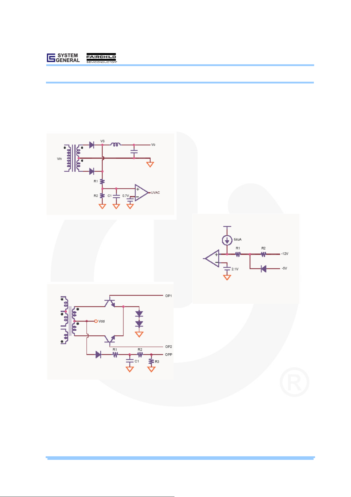
AC Fails Detection
Through a resistor divider, UVAC is connected to the
secondary power transformer for detecting the AC line
condition. Once the voltage of UVAC is lower than 0.7V
for a period of time, such as 200µs, the PG (power-good)
signal is pulled low to indicate an AC line power-down
condition. The voltage amplitude of the PWM switching
Page 14
Product Specification
Power Supply Supervisor + Regulator + PWM
SG6105A
© System General Corp. - 14 - www.sg.com.tw • www.fairchildsemi.com
Version 1.0.1 (IAO33.0072.B0) September 25, 2007
signal in the secondary power transformer is proportional
to the AC line voltage. Adjust the ratio of resistor divider
to decide the threshold of power-down warning. A small
capacitor is connected from UVAC to ground for filtering
the switching noise.
Over-Power Protection (OPP)
The OPP (over-power protection) is used for detecting
over-power and/or short-circuit conditions. When OPPS
voltage (p.4, Note-1) is higher than 2.1V and this situation
exists for longer than 7ms, 6105A pulls the PG low and
locks off the power outputs.
Negative Voltage Protection (NVP)
The NVP provides an under-voltage protection (UVP)for
negative voltage outputs. An under-voltage represents the
phenomenal of the overload condition in negative voltage
output. For example, the –12V output may drop to –10V
during the overload situation. A resistor determining the
threshold of the protection is connected from pin NVP to the
negative voltage output. Via this resistor, NVP outputs a
64µA constant current to the negative voltage output. When
the NVP voltage is over 2.1V and the situation kept for
longer than 7ms, 6105A locks the power outputs off:
VNVP = 64µA × (R1 + R2) – V-12V (1)
The power outputs are locked off when VNVP
≥ 2.1V.
Page 15

Product Specification
Power Supply Supervisor + Regulator + PWM
SG6105A
© System General Corp. - 15 - www.sg.com.tw • www.fairchildsemi.com
Version 1.0.1 (IAO33.0072.B0) September 25, 2007
REFERENCE CIRCUIT
Page 16

Product Specification
Power Supply Supervisor + Regulator + PWM
SG6105A
© System General Corp. - 16 - www.sg.com.tw • www.fairchildsemi.com
Version 1.0.1 (IAO33.0072.B0) September 25, 2007
BOM
Page 17

Product Specification
Power Supply Supervisor + Regulator + PWM
SG6105A
© System General Corp. - 17 - www.sg.com.tw • www.fairchildsemi.com
Version 1.0.1 (IAO33.0072.B0) September 25, 2007
PACKAGE INFORMATION
20 PINS – DIP (D)
θ
e
B
E
A
A2
e
A1
L
b
b1
10
1
D
20
11
E1
Dimensions:
Millimeter Inch
Symbol
Min. T
yp
.Max.Min.T
yp
.Max.
A
5.334 0.210
A
1 0.381 0.015
A
2 3.175 3.302 3.429 0.125 0.130 0.135
b 1.524 0.060
b1 0.457 0.018
D 24.892 26.162 26.924 0.980 1.030 1.060
E 7.620 0.300
E1 6.223 6.350 6.477 0.245 0.250 0.255
e 2.540 0.100
L 2.921 3.302 3.810 0.115 0.130 0.150
eB 8.509 9.017 9.525 0.335 0.355 0.375
θ˚
0° 7° 15° 0° 7° 15°
Page 18

Product Specification
Power Supply Supervisor + Regulator + PWM
SG6105A
© System General Corp. - 18 - www.sg.com.tw • www.fairchildsemi.com
Version 1.0.1 (IAO33.0072.B0) September 25, 2007
 Loading...