

Page 1
SG6
10
查询SG6105供应商
Product Specification
Power Supply Supervisor + Regula tor + PWM SG6105
FEATURES
PC half-bridge (or 494) power supply supervisor +
two 431 + PWM
High integration & few external components
Over-voltage protection for 3.3V, 5V and 12V
Under-voltage protection for 3.3V, 5V and 12V
Under-voltage protection for –12V and/or –5V
Over-power and short-circuit protection
Power-down warning circuitry
Power good circuitry
Delay time for PSON and PG signal
Remote ON/OFF function
On-chip oscillator and error amplifier
Two shunt regulator for 3.3V and 5V-Standby
Latching PWM for cycle-by-cycle switching
Push-pull PWM operation and totem pole outputs
Soft-start and maximum 93% duty cycle
APPLICATIONS
Switching mode power supply for Computers, such
as:
DESCRIPTION
SG6105 controller is designed for switching mode
power supply for desktop PCs. It provides all the
functions necessary to monitor and control the output of
the power supply. Remote ON/OFF control, power good
circuitry, some protection features against over-voltage
and over-power are implemented. It directly senses all the
output rails for OVP without the need of external dividers.
An innovated AC-signal sampling circuitry provides a
sufficient power-down warning signal for PG. A built-in
timer generates accuracy timing for control circuit
including the PS-off delay. The cycle-by-cycle PWM
switching prevents the power transformer from the
saturation and ensures the fastest response for the
short-circuit protection which greatly reduce the stress for
power transistors. Two internal precision TL431 shunt
regulators provide stable reference voltage and driver for
3.3V and 5V-standby regulation. Utilizing minimum
number of external components, the SG6105 includes all
of the functions for push-pull and/or half-bridge topology,
decreasing the production cost and PCB space, and
increasing the MTBF for power supply.
ATX NLX SFX (micro-ATX)
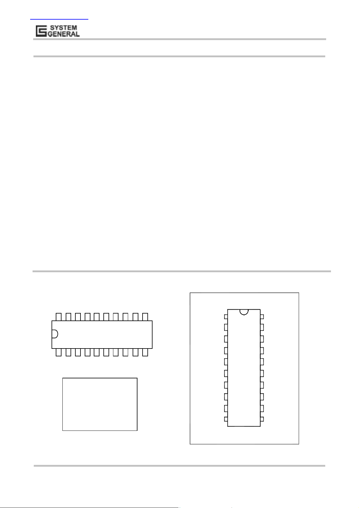
MARKING D IAGRA MS PIN CONFIGURATION
20
XXXXXXXYYWWV
1
T: D = DIP
XXXXXXX: Wafer Lot
YY: Year; WW: Week
V: Assembly Location
5T
PSON
V33
V5
OPP
UVAC
NVP
V12
OP2
OP1
PG
1
2
3
5
6
7
8
9
10
20
19
18
4
17
16
15
14
13
12
11
VCC
RI
SS
IN
COMP
GND
FB1
VREF1
VREF2
FB2
©System General Corp. - 1 - www.sg.com.tw
Version 2.3(IRO33.0011.B0) June 19, 2003
Page 2
Product Specification
Power Supply Supervisor + Regula tor + PWM SG6105
ORDERING INFORMATION
Part Number Package
SG6105D 20-Pin DIP
PIN DESCRIPTIONS
Name Pin Type Function
VCC 20 Supply Supply voltage. 4.5V ~ 5.5V. It is connected to 5V-standby.
PG 10 Logic output
V33 2 Analog input 3.3V over-voltage/under-voltage control sense input.
V5 3 Analog input 5V over-voltage/under-voltage control sense input.
V12 7 Analog input 12V over-voltage/under-voltage control sense input.
OPP 4 Analog input
PSON 1 Logic input
NVP 6 Analog input The protection input for negative output, such as –12V and/or –5V. Trip voltage = 2.1V.
UVAC 5 Analog input AC fail detection, detect main AC voltage under-voltage and/or failure.
COMP 16 Analog output Error amplifier output and the input of the PWM comparator.
IN 17 Analog input The negative input of error amplifier. The positive input of error amplifier is a 2.5V reference voltage.
SS 18 Analog input
OP1/OP2 9/8 Analog output
FB1 14 Analog output Output for first converter regulation loop.
VREF1 13 Analog input Reference comparison input for first converter regulation loop. 2.5V.
FB2 11 Analog output Output for second converter regulation loop.
VREF2 12 Analog input Reference comparison input for second converter regulation loop. 2.5V.
RI 19
GND 15 Supply Ground.
Program.
Analog input
Power Good logic output, 0 or 1 (open-collector). PG = 1 means that the power is good for operation.
The PG delay is 300 msec.
Over-power sense input. This pin is connected to driver transformer or the output of current
transformer. When not in use, this pin should be grounded.
ʳ
Remote On/Off logic input for
msec delay.
PSON = 0 means that the main SMPS is operational.
PSON =1 means that the main SMPS is off and the latch is reset.
The soft-start. It is settable through external capacitor. The current source output at this pin is 8uA and
the voltage is clamped at 2.5V.
The totem-pole output drivers of push-pull PWM. The output are enabled (low) only when the NAND
gate inputs are high, the maximum duty cycle on an output (OP1 or OP2) is 46%.
Connected to external resistor for the reference setting.
RI = 75k ohms.
CPU or controller. Turn on/off the PWM Output after the 7.5 msec / 26
©System General Corp. - 2 - www.sg.com.tw
Version 2.3(IRO33.0011.B0) June 19, 2003
Page 3
Product Specification
Power Supply Supervisor + Regula tor + PWM SG6105
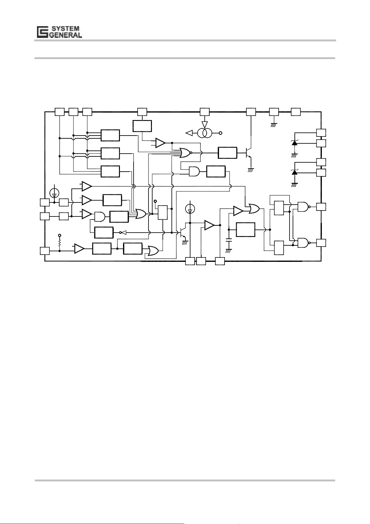
BLOCK DIAGRAM
V33
2 3
V5
V12
7
UVAC
5
19
10
PG
GND
15
VCC
20
RI
NVP
OPP
PSON
14
11
FB1
VREF1 13
FB2
VREF2 12
9
OP1
8
OP2
DSD
UV
Detector
OV
Protector
UV
Protector
COMP
1.4V
3.2V
2.1V
2.4V
_
+
COMP
_
+
COMP
_
+
COMP
_
+
Delay
15msec
On/Off Delay
26msec
7.5msec
Delay
7msec
Delay
7msec
Delay
2msec
5V
64uA
Buffer
6
Buffer
4
Vcc
1
0.7V
COMP
_
+
Vcc
D
CK
2uA
2.5V
18
8uA
SS
IN
Q
R
Vref
Delay
300msec
Delay
3sec
D
_
+
COMP
+
_
Error
Amp
16 17
O.S.C
Q
_
CK
Q
SQ
R
COMP
©System General Corp. - 3 - www.sg.com.tw
Version 2.3(IRO33.0011.B0) June 19, 2003
Page 4
Product Specification
Power Supply Supervisor + Regula tor + PWM SG6105
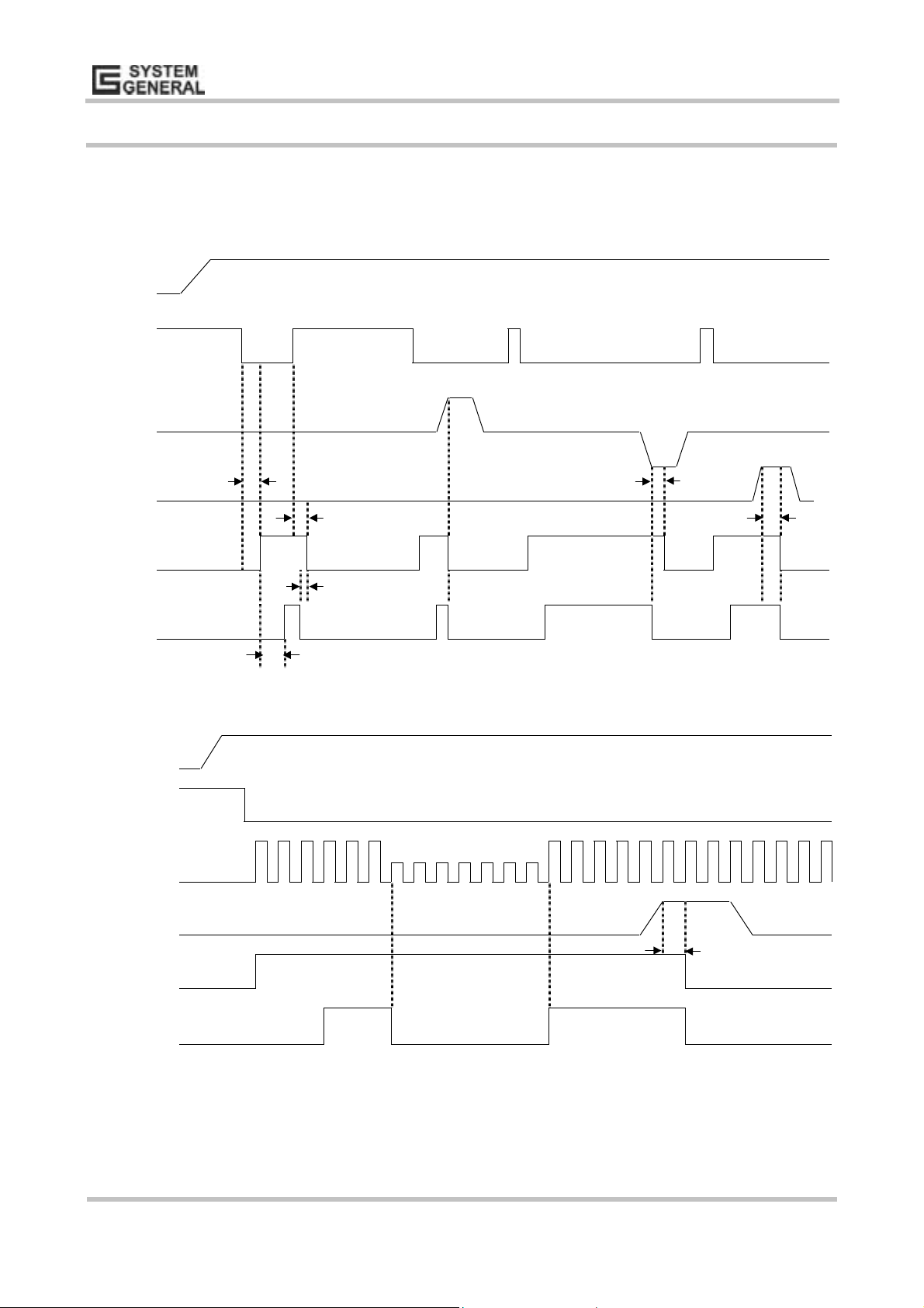
TIMING DIAGRAM
VCC
PSON
3.3V,5V,12V
NVP
t
t
PSON(ON)
t
t
PSON(OFF)
UVP
NVP
SS(on/off)
SS(on/off)
t
PG
tPG
VCC
PSON
UVAC
OPP
PG
t
PSOFF
Voltage < V
UVAC
OPP
©System General Corp. - 4 - www.sg.com.tw
Version 2.3(IRO33.0011.B0) June 19, 2003
Page 5
Product Specification
Power Supply Supervisor + Regula tor + PWM SG6105
ABSOLUTE MAXIMUM RATINGS
Symbol Parameter Value Unit
VCC DC Supply Voltage at Pin 20 16 V
V
FB
I
Output Current at PG, Fb1, Fb2 Pins 30 mA
OUT
P
к
Power Dissipation (TA=25к) 1.5 W
D,25
P
к
Power Dissipation (TA=90к) 0.5 W
D,90
T
Storage Temperature Range -55 to +150
STG
R
Thermal Resistance, Junction-To-Air 82.5
θJA
T
J,MAX
T
A,MAX
T
L
ESD Capability, HBM model 3.0 kV
Note: All voltage values, except differential voltage, are with respect to network ground terminal.
Shunt Regulator Output at Fb1, Fb2 Pins 16 V
Operating Junction Temperature 150
Operating Ambient Temperature -30 to +125
Lead Temperature (Soldering, 10sec) 260
к
к
к
к
к
/W
RECOMMENDED OPERATING CONDITIONS
Symbol Parameter Value Unit
V
CC
V
FB
T
Operating Ambient Temperature Range -25 to +85
OPER
DC Supply Voltage at Pin 20 4.5 to 5.5 V
Shunt Regulator Output at Fb1, Fb2 Pins 4 to 16 V
к
ELECTRICAL CHARACTERISTICS (VCC = 5V, TA = 25°°°°C)
Symbol Parameter Test Condition Min. Typ. Max. Unit
I
CC
V
Over-Voltage Protection 3.3V - 3.9 4.1 4.3 V
OVP1
V
Over-Voltage Protection 5V - 5.8 6.1 6.5 V
OVP2
V
Over-Voltage Protection 12V - 13.9 14.5 14.9 V
OVP3
V
Under-Voltage Protection 3.3V - 2.0 2.6 2.8 V
UVP1
V
Under-Voltage Protection 5V - 3.0 3.6 3.9 V
UVP2
V
Under-Voltage Protection 12V - 6.0 7.2 8.0 V
UVP3
V
Under-Voltage Sense 3.3V for PG Low - 2.5 2.8 3.0 V
UVS1
V
Under-Voltage Sense 5V for PG Low - 4.0 4.3 4.5 V
UVS2
V
Under-Voltage Sense 12V for PG Low - 9.4 10.1 10.4 V
UVS3
V
* 1 Over-Power Protection. V
OPPS
V
Negative Voltage Protection: Voltage Level - 2.0 2.1 2.2 V
NVP
I
Negative Voltage Protection: Source Current RI = 75kΩ 57 64 72 uA
NVP
t
Timing for Over-Voltage Protection RI = 75kΩ 0.37 0.7 1.35 ms
OVP
t
Timing for Under-Voltage Protection RI = 75kΩ 0.8 2.4 3.75 ms
UVP
t
UVS
t
Timing for Over-Power-Protection RI = 75kΩ 3.3 7 11.3 ms
OPP
t
Timing for Negative Voltage Protection RI = 75kΩ 3.3 7 10.2 ms
NVP
Note *1: V
Total Supply Current PG High - 5 10 mA
= 1.5V 2.02 2.4 2.66 V
UVAC
Timing for Under-Voltage Sense for PG Low RI = 75kΩ 0.37 1.2 1.88 ms
= (2/3) x V
OPPS
+ (1/3) x V
OPP
UVAC
;
©System General Corp. - 5 - www.sg.com.tw
Version 2.3(IRO33.0011.B0) June 19, 2003
Page 6

Product Specification
Power Supply Supervisor + Regula tor + PWM SG6105
Shunt Regulator (FB1, VREF1, FB2, VREF2)
Symbol Parameter Test Condition Min. Typ. Max. Unit
V
Reference Voltage IFB = 0.5mA, TA = 25к 2.475 2.5 2.525 V
REF
*2
V
Deviation of V
DEV, I
* 2
V
DEV, T
R
EGLI-FB
I
OUT-FB
*2
*2
Deviation of V
Line Regulation 4 < VFB < 16V - 1 - mV/V
Output Sinking Current Capability VFB > 2V 10 - - mA
Note *2: Not tested in production test.
Over Load Current IFB = 0.5mA to 10mA - - 20 mV
REF
Over Temperature TA = -25к to 85к - 10 30 mV
REF
Power Good Section
Symbol Parameter Test Condition Min. Typ. Max. Unit
tPG Timing for PG Delay RI = 75kΩ 200 300 400 ms
V
UVAC Voltage Sense for PG - 0.65 0.7 0.75 V
UVAC
*2
t
PG Good Output Rising Time CL = 100pF - 1 - us
R
*2
t
PG Good Falling Time CL = 100pF - 300 - ns
F
V
Power Good Output Saturation Level IPG = 5mA - - 0.5 V
OL2
I
Power Good Leakage Current Collector VPG = 5V - - 1 uA
ON2
Remote On/Off
Symbol Parameter Test Condition Min. Typ. Max. Unit
V
PSON Input Threshold Level - 1 1.4 2.0 V
PSON
I
Remote Input Driving Current - - - 0.5 mA
PSON
t
PSON(ON)
t
PSON(OFF)
t
Timing PG low to Power Off RI = 75kΩ 1.5 2 6.3 ms
PSOFF
Timing PSON to On/Off
On
Off (PS-off)
RI = 75kΩ
17
5
26
7.5
45
28.8
ms
Error Amplifier
Symbol Parameter Test Condition Min. Typ. Max. Unit
V
Reference Voltage - 2.45 2.5 2.55 V
2.5
*2
I
Input Bias Current - - - 0.1 uA
IB
* 2
A
VOL
BW
PSRR
* 2
* 2
Open-Loop Voltage Gain - 50 60 - dB
Unity Gain Bandwidth - 0.3 1 - MHz
Power Supply Rejection Ratio - 50 - - dB
Oscillator Section
Symbol Parameter Test Condition Min. Typ. Max. Unit
F
PWM Frequency RI = 75kΩ 60 65 70 KHz
OSC
Soft-Start Section
Symbol Parameter Test Condition Min. Typ. Max. Unit
ISS Charge Current RI = 75kΩ 6 8 9.3 uA
©System General Corp. - 6 - www.sg.com.tw
Version 2.3(IRO33.0011.B0) June 19, 2003
Page 7
Product Specification
Power Supply Supervisor + Regula tor + PWM SG6105
Comparator Section
Symbol Parameter Test Condition Min. Typ. Max. Unit
DC Duty Cycle - 85 - 93 %
PWM Output Section (OP1, OP2)
Symbol Parameter Test Condition Min. Typ. Max. Unit
VOL Output Voltage Low Io = 5mA - - 0.5 V
VOH Output Voltage High V12 = 12V 4 - - V
RO Output Impedance of VOH - 1.5 - 3.3 kΩ
©System General Corp. - 7 - www.sg.com.tw
Version 2.3(IRO33.0011.B0) June 19, 2003
Page 8
Product Specification
Power Supply Supervisor + Regula tor + PWM SG6105
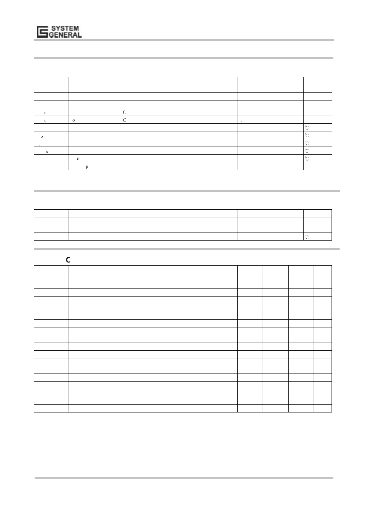
APPLICATION 1
MAIN
Transformer
STBY
Transformer
5Vsb
+
+
+
+
UVAC
3.3V
VREF2
FB2
+
VREF1
FB1
OP1
SG6105
V33
V5
V12
VCC
PG
PSON
NVP
RI
47~100ohm
1Kohm
-12V
12V
5V
3.3V
5Vsb
Pok
PSon
-12V
-5V
Vdd
OP2
OPP
GND
IN
COMP
SS
5V
12V
©System General Corp. - 8 - www.sg.com.tw
Version 2.3(IRO33.0011.B0) June 19, 2003
Page 9

Product Specification
Power Supply Supervisor + Regula tor + PWM SG6105
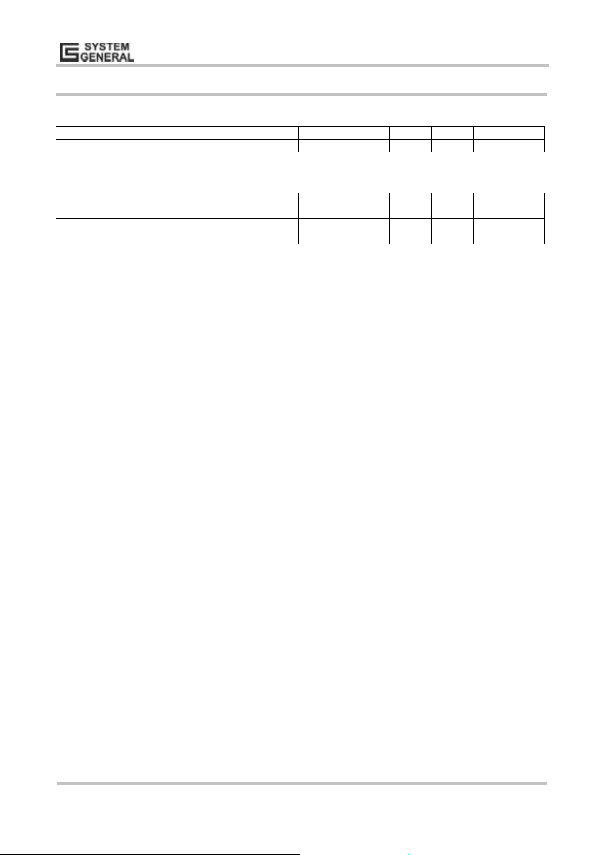
APPLICATION 2
OP1
2
C45
2 3
R76
FB1
VREF1
R83
C56
R86
R87
-12V
-5V
21
D42
R92
4
U5
1
PSON
3.3V
5V
OPP
UVAC
R96
12V
OP2
OP1
R100
PG
R64
5 6 7 8
RI NC FB GND
C78
+
R70
U6
1
PSON
2
V33
3
V5
4
OPP
5
UVAC
6
NVP
7
V12
8 13
OP2 VREF1
9
OP1
10 11
PG FB2
SG6105
GateVDDNCSEN
1234
R68
D31
2 1
54
VCC
RI
SS
IN
COMP
GND
FB1
VREF2
U4
SG6848
R67
R66
R71
R69
D32
Q141
2 1
23
8
6
2
21
D37
C51
+
R84
L13
1
2
C57
+
D41
5VSB
C60
20
R90
19
C62
18
17
R93
16
15
14
FB1
VREF1
12
VREF2
FB2
HHV
C48
10
T7
E16-D
1
21
D38
C52
+
R85
R91
C63
5V
R94
12V
R97
31
VR3
2
VREF2
D26
1 3
Q12
D27
2 1
D28
2 1
2 1
D29
C42
2 1
+
Q13
1 3
2
OP2
D33
2 1
R73
FB2
C79
+
+
3.3VSENCE
R77
3 2
D39
2 1
UVAC
C69
R104
2 1
D47
21
Q20
R112
2
R113
C74
R109R105 R106
OPP
R61
R62
C39
R65
D30
2 1
423
6
5108
21
D34
+
C49
R79
1
Q15
R103
D45
2 1
12
L14
D48
R101
C67
3
C73
1
+
R115
C76
+
R116
T6
9
21
D35
+
C50
R75R74
R78
C55
13
R81 R82
7
8
R98
32
C65 C66
78
C70
+
R107
12
C75
+
5V
C53
VZ312VZ4
R88C59
1
Q18
56
L19
R80
1
3 2
Q16
D40
2 1
12
10
11
V5
D46
2 1
C64
R95
1
32
Q17
1
32
R102
Q19
C68
10 9
12
L18
12
L20
3.3V
12
L17
C72
+
R110
12V
CN2
123
12
F2
C40
R63
12
L11
C47
2
C54
+
C58
5
T8
14
9
R89
C61
R99
3
4
V5
C71
+
R111
1
C77
+
12
L12
T5
2134
C44
C46
12
TR2
4
BD1
3
1
+
12
HHV
D43
D44
2 1
2 1
12
L15
12
L16
-12V
2
U7
VI
LM7905
GND
VO
3
-5V
©System General Corp. - 9 - www.sg.com.tw
Version 2.3(IRO33.0011.B0) June 19, 2003
Page 10

Product Specification
Power Supply Supervisor + Regula tor + PWM SG6105
Example of Using SG6105 for the ATX
Power Supply
Protection against over-voltage, short-circuit and
fault conditions is mandatory in PC power supplies. These
protection circuits can be realized by using many discrete
components and comparators, which occupy a lot of PCB
space and also add to assembling costs. This single chip
controller IC provides complete protection circuits, shunt
regulators, and PWM control function and with less
number of components. SG6105 is an ideal controller IC
for PC switching mode power supplies.
threshold level. PG pin goes high when the above
condition is reached. A 2K pull up resistor may connect to
5V.
The VCC can be supplied from the 5V-standby.
When the VCC voltage is higher than 7V, besides the
shunt regulator, the circuit of SG6105 will be
shutdown and reset. No extra power supply is
needed.
Two internal high precision 431 shunt regulators are
built-in. It provides stable reference voltages.
Complete PWM control circuitry including the error
amplifier for push-pull or half-bridge operation.
The features and benefits of this device are listed
below:
Supervisory Circuit Operation
Over-voltage and under-voltage protection for 3.3V,
5V and 12V without external divider
Over-power protection.
UV protection for –12V and/or –5V.
Power-down warning for power good signal.
Power good signal and power-fail lockup
Remote on/off control.
Delay time for PSON and PS-off signal.
Two shunt regulator for 3.3V and 5V-Standby
regulation.
Complete pulse width modulation (PWM) control
circuitry.
On-chip oscillator.
Programmable Soft-Start.
Maximum 93% duty cycle
Few external components
More reliable system
Little space on PCB
Easy trouble-shooting and implementation
FEATURE DESCRIPTIO NS
Over voltage protection can be implemented without
any additional components. Over-voltage sense
Levels or 3.3V, 5V, 12V are 4.1V, 6.1V, 14.5V
respectively.
Over current and/or short circuit protection can also
be achieved by using over-power protection, in
which OPP pin is connected to the current
transformer (driver transformer).
The power good signal is asserted to indicate the
3.3V, 5V and 12V is above the under voltage
The PC generates the remote ON/OFF logic (PSON),
which is “Low” for power supply “On” and “High” to
switch off the power supply. The remote ON/OFF is
connected to PSON input.
APPLICATION GUIDES
Introduction
The application guide shows the key-feature of
SG6105 and illustrates how to use in an ATX switching
mode power supply (SMPS). SG6105 is suitable for
half-bridge, push-pull topology. It incorporates with a
4-channel supervisor, including 5V-standby. The PWM
section of SG6105 comprises a built-in 65kHz oscillator
and high immunity circuits, which protect the system
from noise interference and provide more noise margins
for improper PCB layout. SG6105 has OVP and UVP for
12V, 5V and 3.3V. Besides, the NVP is used for negative
voltage protection, such as –12V and/or –5V. The UVAC
(AC fails detection) is applied to detect AC line condition.
Two built-in internal precision TL431 shunt regulators
can be used for 3.3V or 5V auxiliary standby power.
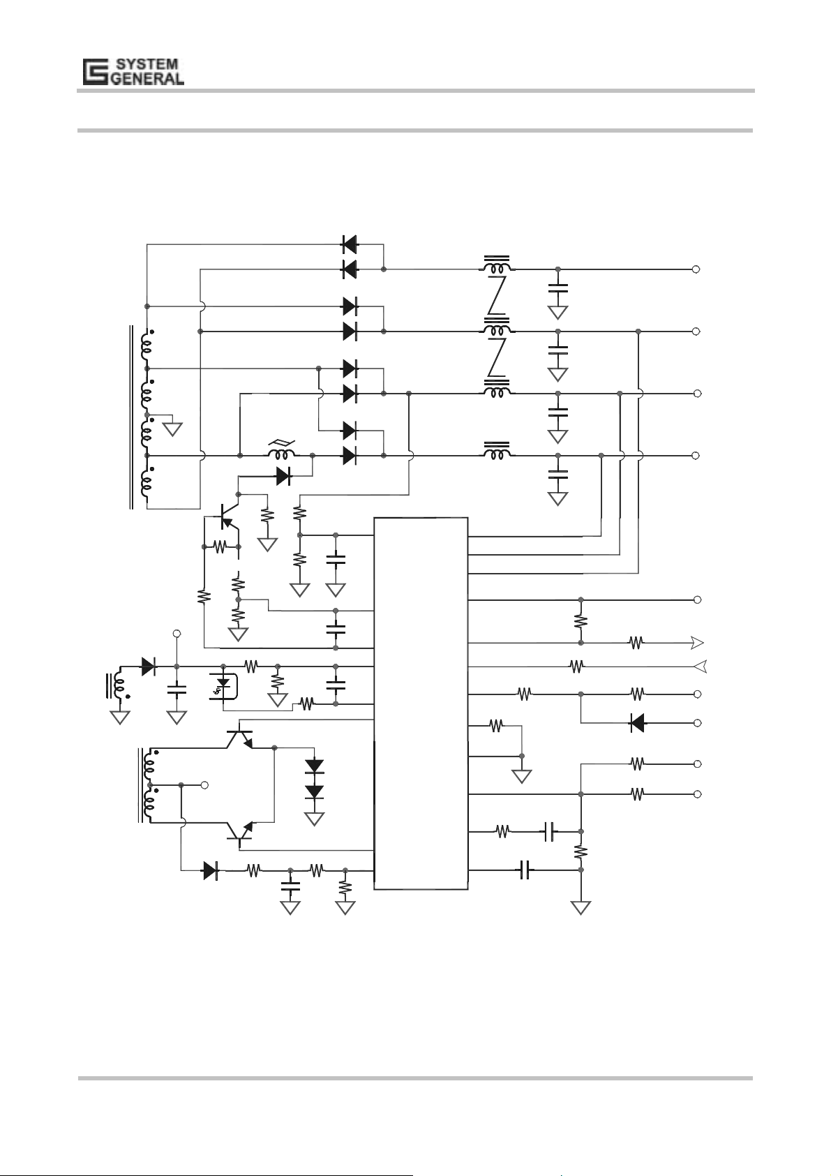
AC Fails Detection
Through a resistor divider, UVAC is connected to
the secondary power transformer for detecting the AC line
condition. Once the voltage of UVAC is lower than 0.7V
for a period of time, such as 200usec, the PG (power good)
signal will be pulled low to indicate an AC line
power-down condition. The voltage amplitude of the
©System General Corp. - 10 - www.sg.com.tw
Version 2.3(IRO33.0011.B0) June 19, 2003
Page 11
Product Specification
Power Supply Supervisor + Regula tor + PWM SG6105
PWM switching signal in the secondary power
transformer is proportional to the AC line voltage. Adjust
the ratio of resistor divider to decide the threshold of
power-down warning. A small capacitor is connected
from UVAC to ground for filtering the switching noise.
VS
Vin
R1
R2
C1
0.7V
Vo
+
UVAC
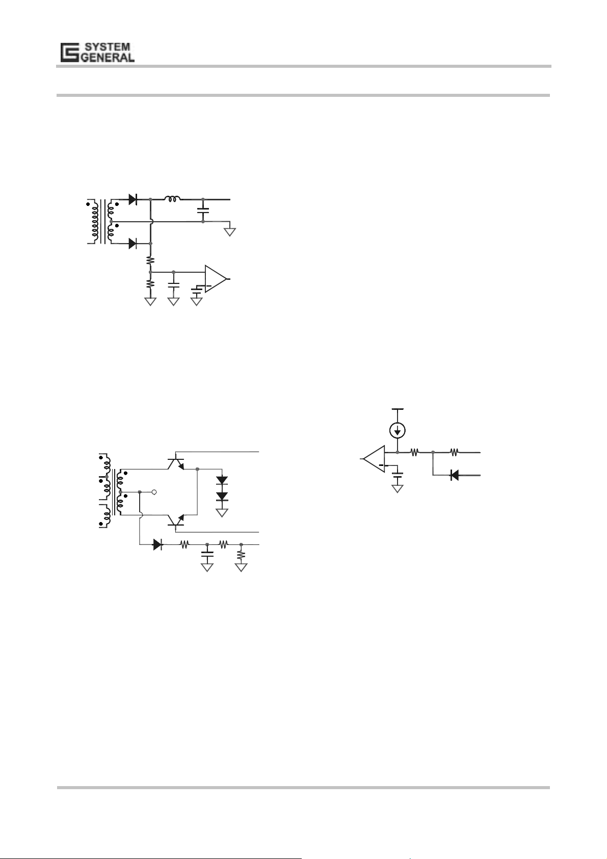
Negative Voltage Protection
The NVP provides an UVP (under voltage protection)
for negative voltage outputs. An under-voltage represents
the phenomenal of the overload condition in negative
voltage output. For example, the –12V output may drop
to –10V during the overload situation. A resistor
determining the threshold of the protection is connected
from pin NVP to the negative voltage output. Via this
resistor, NVP outputs a 64uA constant current to the
negative voltage output. When the NVP voltage is over
2.1V and the situation kept for longer than 7 msec, 6105
will lock the power outputs off.
VNVP = 64 uA × (R1 + R2) – V-12V
Over Power Protection (OPP)
The OPP (over power protection) is used for
detecting over power and/or short-circuit conditions.
When OPPS voltage (p.4, Note-1) is higher than 2.1V and
this situation existed for longer than 7 msec, 6105 will
pull the PG low and lock off the power outputs.
OP1
Vdd
R1 R2
C1
OP2
OPP
R3
The power outputs will be locked off when VNVP ≥
2.1V.
64uA
+
2.1V
R2R1
-12V
-5V
©System General Corp. - 11 - www.sg.com.tw
Version 2.3(IRO33.0011.B0) June 19, 2003
Page 12
Product Specification
yp
b
b
Power Supply Supervisor + Regula tor + PWM SG6105
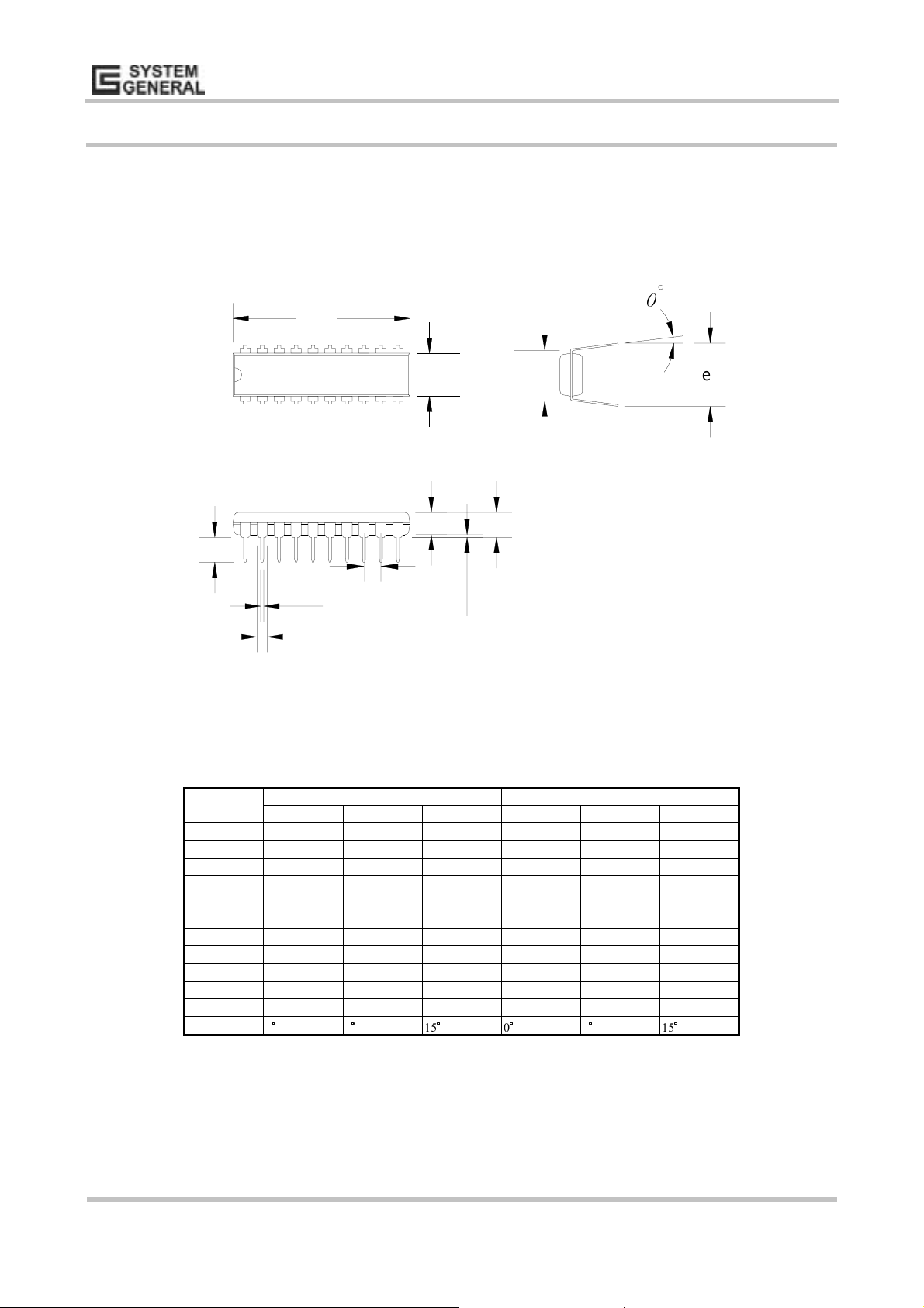
MECHANICAL DIMENSIONS
20 PINS – DIP (D)
Ӱ
D
20
11
E1
B
E
e
Dimension
1
10
A2
A
L
e
b1
A1
b
Symbol
A 5.334 0.210
A1 0.381 0.015
A2 3.175 3.302 3.429 0.125 0.130 0.135
1.524 0.060
1 0.457 0.018
D 24.892 26.162 26.924 0.980 1.030 1.060
E 7.620 0.300
E1 6.223 6.350 6.477 0.245 0.250 0.255
e 2.540 0.100
L 2.921 3.302 3.810 0.115 0.130 0.150
e
8.509 9.017 9.525 0.335 0.355 0.375
θ˚ 0
Min. T
. Max. Min. Typ.Max.
7
15
0
7
15
©System General Corp. - 12 - www.sg.com.tw
Version 2.3(IRO33.0011.B0) June 19, 2003
Page 13

Product Specification
Power Supply Supervisor + Regula tor + PWM SG6105
DISCLAIMERS
LIFE SUPPORT
System General’s products are not designed to be used as components in devices intended to support or sustain
human life. Use of System General’s products in components intended for surgical implant into the body, or other
applications in which failure of the System General’s products could create a situation where personal death or injury may
occur, is not authorized without the express written approval of System General’s Chief Executive Officer. System
General will not be held liable for any damages or claims resulting from the use of its products in medical applications.
MILITARY
System General's products are not designed for use in military applications. Use of System General’s products in
military applications is not authorized without the express written approval of System General’s Chief Executive Officer.
System General will not be held liable for any damages or claims resulting from the use of its products in military
applications.
RIGHT TO MAKE CHANGES
System General reserves the right to change this document and/or this product without notice. Customers are advised
to consult their System General sales representative before ordering.
©System General Corp. - 13 - www.sg.com.tw
Version 2.3(IRO33.0011.B0) June 19, 2003
 Loading...