

System General SG5701DZ, SG5701TZ Schematic [ru]
Product Specification
Low Cost Green-Mode PWM Controller for Flyback Converters
SG5701
FEATURES
Green-Mode PWM
Supports the “Blue Angel” Standard
Low Start-up Current (10uA)
Low Operating Current (2mA)
Leading-Edge Blanking
Constant Output Power Limit
Universal Input
Built-in Synchronized Slope Compensation
Current Mode Operation
Cycle-by-cycle Current Limiting
Under Voltage Lockout (UVLO)
Programmable PWM Frequency
Gate Output Voltage Clamped at 17V
Low Cost
Few External Components Required
Small SOT-26 Package
APPLICATIONS
General-purpose switching mode power supplies and
flyback power converters, such as
Battery chargers for cellular phones, cordless phones,
PDAs, digital cameras, and power tools
Power adapters for ink jet printers, video game
consoles, and portable audio players
Open-frame SMPS for TV/DVD standby and other
auxiliary supplies, home appliances, and consumer
electronics
Replacements for linear transformers and RCC
SMPS
PC 5V standby power.
DESCRIPTION
This highly-integrated PWM controller provides
several special enhancements designed to meet the low
standby-power needs of low-power SMPS. To minimize
standby power consumption, the proprietary green-mode
function provides off-time modulation to linearly
decrease the switching frequency under light-load
conditions. This green-mode function enables the power
supply to easily meet even the strictest power
conservation requirements.
The BiCMOS fabrication process enables reducing
the start-up current to 10uA, and the operating current to
2mA. To further improve power conservation, a large
start-up resistance can be used. Built-in synchronized
slope compensation ensures the stability of peak current
mode control. Proprietary internal compensation provides
a constant output power limit over a universal AC input
range (90VAC to 264VAC). Pulse-by-pulse current
limiting ensures safe operation even during short-circuits.
To protect the external power MOSFET from being
damaged by supply over voltage, the SG5701’s output
driver is clamped at 17V. SG5701 controllers can be used
to improve the performance and reduce the production
cost of power supplies. The SG5701 is the best choice for
replacing linear and RCC-mode power adapters. It is
available in 8-pin DIP and 6-pin SOT-26 packages.
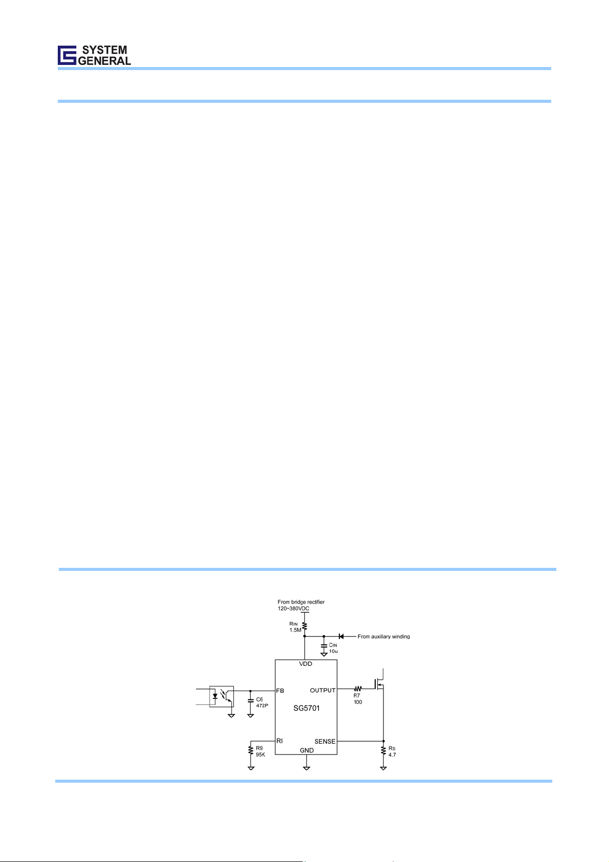
TYPICAL APPLICATION
© System General Corp. - 1 - www.sg.com.tw
Version 1.0(IAO33.0025.B1) Mar. 28, 2006
Product Specification
N
N
Low Cost Green-Mode PWM Controller for Flyback Converters
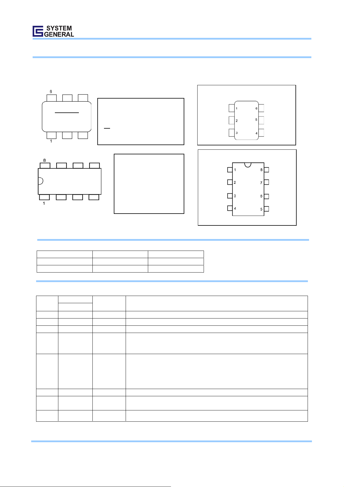
MARKING DIAGRAMS PIN CONFIGURATION
AAEMW
AAE:SG5701
M: Mask Version
W: Week
: Lead Free
GND
FB
RI
SOT-26
GATE
VDD
SENSE
SG5701
SG5701DP
XXXXXXXXYWWV
D: D=DIP
P : Z =Lead Free
Null=Regular Package
XXXXXXXX: Wafer Lot
Y: Year
WW: Week
V: Assembly Location
GATE
VDD
C
SENSE
ORDERING INFORMATION
Part Number PWM Frequency Package
SG5701TZ 70kHz 6-Pin SOT-26 (Lead Free)
SG5701DZ 70kHz 8-pin DIP-8 (Lead Free)
PIN DESCRIPTIONS
Name
GATE 1 / (6) Driver Output The totem-pole output driver for driving the power MOSFET.
VDD 2 / (5) Supply Power supply.
NC 3 NC pin.
SENSE 4 / (4) Analog Input
RI 5 / (3)
NC 6 NC pin.
FB 7 / (2) Analog Input
GND 8 / (1) Supply Ground.
Pin No.
DIP-8 / (SOT-26)
Type Function
Current sense. This pin senses the voltage across a resistor. When the voltage reaches
the internal threshold, PWM output is disabled. This activates over-current protection.
This pin also provides current amplitude information for current-mode control.
A resistor connected from the RI pin to ground will generate a constant current source for
Analog
Input/Output
the SG5701. This current is used to charge an internal capacitor, to determine the
switching frequency. Increasing the resistance will reduce the amplitude of the current
source and reduce the switching frequency. A 95kΩ resistor R
current I
Feedback. The FB pin provides the output voltage regulation signal. It provides feedback
to the internal PWM comparator, so that the PWM comparator can control the duty cycle.
and a 70kHz switching frequency.
i
DIP-8
GND
results in a 50uA constant
i
FB
C
RI
© System General Corp. - 2 - www.sg.com.tw
Version 1.0(IAO33.0025.B1) Mar. 28, 2006
Product Specification
Low Cost Green-Mode PWM Controller for Flyback Converters
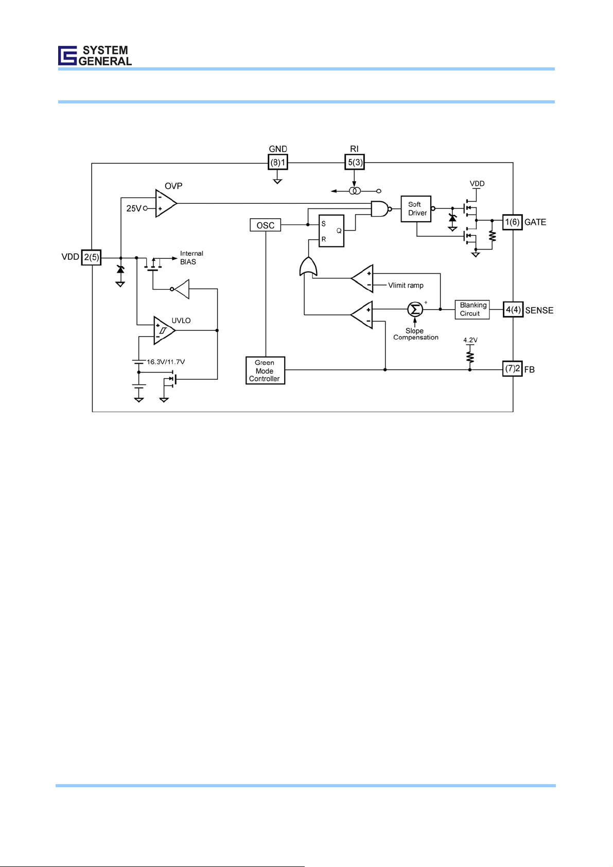
BLOCK DIAGRAM
SG5701
© System General Corp. - 3 - www.sg.com.tw
Version 1.0(IAO33.0025.B1) Mar. 28, 2006

Product Specification
Low Cost Green-Mode PWM Controller for Flyback Converters
ABSOLUTE MAXIMUM RATINGS
Symbol Parameter Value Unit
VDD DC Supply Voltage * 30 V
VFB Input Voltage to FB Pin -0.3 to 6 V V
V
Input Voltage to Sense Pin -0.3 to 6V V
SENCE
TJ Operating Junction Temperature 150 ℃
PD Power Dissipation at TA=85℃
RθJA Thermal Resistance (Junction to Air)**
T
Storage Temperature Range -55 to +150 ℃
STG
T
R
ESD Capability, HBM Model 3.0 kV
* All voltage values, except differential voltages, are given with respect to the network ground terminal.
**Thermal JA test board size: SOT 18×12×1.6mm/FR4; DIP 40×35×1.6mm/FR4
Peak Reflow Temperature
SOT-26 247
DIP-8 478
SOT-26 263
DIP-8 136
Pb free 260(+5/-0)
Pb 230(+5/-0)
mW
°C/W
°C
SG5701
Stress beyond those listed under “ absolute maximum ratings” may cause permanent damage to the device.
RECOMMENDED OPERATING CONDITIONS
Symbol Parameter Value Unit
VDD DC Supply Voltage ≦24 V
TA Operating Ambient Temperature -30 to +105 ℃
ELECTRICAL CHARACTERISTICS (TA = 25°C, VDD=15V)
VDD Section
Symbol Parameter Test Condition Min. Typ. Max. Unit
VOP Continuously Operation Voltage 24 V
V
Start Threshold Voltage TA=25°C 15.3 16.3 17.3 V
TH(ON)
V
Min. Operating Voltage TA=25°C 10.9 11.7 12.5 V
DD(MIN)
I
Startup Current VDD = V
DD-ST
I
Operating Supply Current VDD = 15V 2 5 mA
DD-OP
V
VDD Clamp Voltage 24.5 25 26.5 V
DD-CLAMP
– 0.10V 10 30 uA
DD-ON
Feedback Input Section
Symbol Parameter Test Condition Min. Typ. Max. Unit
IOZ Zero Duty Cycle Input Current 1.3 2.0 mA
VOP Open Loop Voltage 4.2 V
© System General Corp. - 4 - www.sg.com.tw
Version 1.0(IAO33.0025.B1) Mar. 28, 2006
Product Specification
Low Cost Green-Mode PWM Controller for Flyback Converters
SG5701
Current Sense Section
Symbol Parameter Test Condition Min. Typ. Max. Unit
ZCS Input Impedance 10 kΩ
TPD Delay to Output 60 100 nsec
V
Current Limit Flatten Threshold Voltage 1.0 V
TH,FLT
V
Current Limit Valley Threshold Voltage 0.80 0.85 0.90 V
TH,VALLEY
Oscillator Section
Symbol Parameter Test Condition Min. Typ. Max. Unit
F
Frequency RI=95kΩ 65 70 75 kHz
OSC
F
OSC-GREEN
IG Green-Mode FB Input Current 1.05 mA
IN
SG Green-Mode Modulation Slope RI=95kΩ 300 Hz/uA
FDY Frequency Variation versus VDD Deviation VDD=12 to 20V 0.02 2 %
FDT Frequency Variation versus Temp. Deviation TA=-30 to 105 ℃ 2 %
Green-Mode Frequency RI=95kΩ 13 15 kHz
Green-Mode Start Threshold FB Input Current
= 0.3mA for a Maximum Duty Cycle
I
n
0.85 mA
PWM Section
Symbol Parameter Test Condition Min. Typ. Max. Unit
DC
Maximum Duty Cycle 70 75 80 %
(MAX)
DC
Minimum Duty Cycle - 1 2 %
(MIN)
BNK Leading-Edge Blanking Time 200 nsec
Output Section
Symbol Parameter Test Condition Min. Typ. Max. Unit
VOL Output Voltage Low VDD=15V, Io=20mA 1.5 V
VOH Output Voltage High VDD=15V, Io=20mA 8 V
TR Rising Time VDD=15V, CL=1nF 250 350 nsec
TF Falling Time VDD=15V, CL=1nF 60 150 nsec
V
Output Clamp Voltage VDD=20V 16 17 18 V
CLAMP
© System General Corp. - 5 - www.sg.com.tw
Version 1.0(IAO33.0025.B1) Mar. 28, 2006
 Loading...