

Page 1

SYS TEC electronic GmbH
L-1589e-04 Hardware Manual ECUcore-1021
Page 1/30
Classification: Release
ECUcore-1021
Hardware Manual
Document Revision: L-1589e-04
Disclaimer:
All data, information and technical specifications contained in this document has been subjected to a
thorough examination. The information in the document is current at the time of publication as long as
nothing else is explicitly stated. However no liability is given for the correctness, completeness and
topicality of the contents.
Page 2
SYS TEC electronic GmbH
L-1589e-04 Hardware Manual ECUcore-1021
Page 2/30
Classification: Release
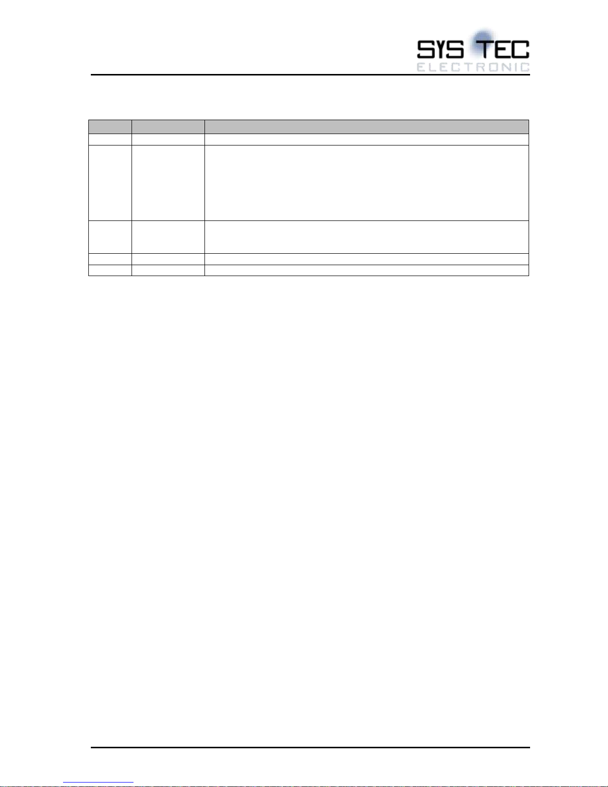
Revision History
Version
Date
Changes
01
17.09.2014
Created (Module revision 4377.0)
02
17.03.2015
Changes to module revision 4377.1 added:
- Pin connector: Signal IFC_AD15 and FTM2_EXTCLK can be supported
now (optional order number) (sec. 2.4.2)
- USB3.0: AC coupling capacitors are supported on-board (sec. 3.5)
- SDC: Feature set of SDC corrected. (sec. 3.12)
- DSM: This feature is prepared for future use, but not supported in the latest
version. (sec. 3.13)
03
11.03.2016
- Block diagram changed
- Freescale changed to NXP
- sec. 4 (Application Carrier Board) added
04
23.01.2017
Alternate pin names of IFC interface are added to Table 5 and Table 6.
Page 3

SYS TEC electronic GmbH
L-1589e-04 Hardware Manual ECUcore-1021
Page 3/30
Classification: Release
List of Abbreviations
ADC Analog digital converter
AI Analog Input
AO Analog Output
BSP Board Support Package
CAN Controller Area Network (according to ISO 11898-1:2003 and ISO 11898-2:2003)
CPU Central Processing Unit
DSM Deep Sleep Mode
EEPROM Electrically Erasable Programmable Read-Only Memory
eMMC embedded Multimedia card
EN European Norm
ETH Ethernet
FB Function Block
GB Giga Byte (1024 x 1MB)
Gb Giga bit
GbE Gigabit Ethernet
GND Ground Reference potential
GPIO General Purpose Input Output
HW Hardware
IEC International Electro technical Commission
I/O Input/Output
I2C Inter-integrated circuit
I2S Integrated Interchip Sound
kB Kilo Byte (1024 byte)
MAC Media Access Controller (e.g. Ethernet controller)
MB Mega Byte (1024 x 1kB)
MDI Media Dependent Interface
nc not connected
OS Operating System
PCB Printed Circuit Board
PDO Process Data Object
PMIC Power Management Integrated Circuit
PLC Programmable Logical Controller
PWM Pulse Width Modulation
RAM Random-Access Memory
RGMII Reduced Gigabit Media-Independent Interface
ROM Read-Only Memory
RTC Real Time Clock
RX Receive
SAI Synchronous Audio Interface
SD Secure Digital
SDC System Diagnostics Controller
sec Seconds
SGMII Serial Gigabit Media-Independent Interface
SIO Serial Input Output
SIL Safety integrity level
SPI Serial Peripheral Interface
SW Software
tbd to be defined
TX Transmit
UART Universal Asynchronous Receiver Transmitter
Page 4

SYS TEC electronic GmbH
L-1589e-04 Hardware Manual ECUcore-1021
Page 4/30
Classification: Release
Contents
List of Abbreviations ............................................................................................................................. 3
List of Tables ......................................................................................................................................... 4
List of Figures ........................................................................................................................................ 5
Reference documents ........................................................................................................................... 6
1 Introduction .................................................................................................................................... 7
2 Product Description ....................................................................................................................... 8
2.1 Orderable parts ........................................................................................................................ 8
2.2 Technical Data ......................................................................................................................... 9
2.3 Block Diagram ........................................................................................................................ 12
2.4 Module connector and pin assignment .................................................................................. 14
2.4.1 Connector type for the Carrier board ................................................................................ 14
2.4.2 Pin assignment row A and row B ...................................................................................... 14
2.5 Mechanical Dimensions and Heat spreader .......................................................................... 21
3 Design-in Considerations ............................................................................................................ 23
3.1 Power Supply Design considerations .................................................................................... 23
3.2 Power-on RESET and RESET Configurations ...................................................................... 23
3.3 Manual RESET (/MR) ............................................................................................................ 23
3.4 System Booting ...................................................................................................................... 23
3.5 General interface design consideration ................................................................................. 23
3.6 PCI Express ........................................................................................................................... 25
3.7 SGMII ..................................................................................................................................... 25
3.8 SGMII/SATA ........................................................................................................................... 25
3.9 ETHERNET Interface considerations .................................................................................... 25
3.10 I2C Interface considerations .................................................................................................. 25
3.11 Temperature sensor ............................................................................................................... 26
3.12 System Diagnostics Controller (SDC, optional) ..................................................................... 26
3.12.1 Window-Watchdog timer ................................................................................................... 26
3.12.2 Real Time Clock (RTC) ..................................................................................................... 26
3.13 Deep sleep mode considerations ........................................................................................... 26
3.14 Thermal Design considerations ............................................................................................. 27
4 Application Carrier Board (optional) .......................................................................................... 28
5 Release and Comments ............................................................................................................... 30
List of Tables
Table 1: Orderable parts ............................................................................................................................... 8
Table 2: Technical data .............................................................................................................................. 11
Table 3: Overview to primary and alternative signal functions of LS1021A signal groups ........................ 13
Table 4: Carrier board plug-in connector .................................................................................................... 14
Table 5: Connector pin assignment (row A) ............................................................................................... 17
Table 6: Connector pin assignment (row B) ............................................................................................... 20
Table 7: Mechanical mounting material ...................................................................................................... 22
Table 8: Overview of configured on-board power rails ............................................................................... 23
Table 9: High-speed interface trace lengths ............................................................................................... 24
Table 10: I2C line pull-up resistors ............................................................................................................. 26
Table 11: I2C device addresses and bit rates ............................................................................................ 26
Page 5

SYS TEC electronic GmbH
L-1589e-04 Hardware Manual ECUcore-1021
Page 5/30
Classification: Release
List of Figures
Figure 1: Block diagram ECUcore-1021 ..................................................................................................... 12
Figure 2: Module dimension and location of Module connector on Carrier Board ..................................... 21
Figure 3: Carrier board plug-in connector physical dimension ................................................................... 22
Figure 4: Mounting example of Module, Carrier Board and heat spreader ................................................ 22
Figure 5: Heat spreader with mounted heat sink (dimension and details) ................................................. 27
Figure 6: Heat spreader with mounted heat sink (example) ...................................................................... 27
Figure 7: Block diagram ECUcore-1021 with Application Carrier Board .................................................... 28
Page 6

SYS TEC electronic GmbH
L-1589e-04 Hardware Manual ECUcore-1021
Page 6/30
Classification: Release
Reference documents
/1/ NXP: LS1021A Reference Manual
/2/ NXP: LS1021A Data Sheet
/3/ PCIMG: COMExpress Carrier Design Guide Rev.2.0
Page 7

SYS TEC electronic GmbH
L-1589e-04 Hardware Manual ECUcore-1021
Page 7/30
Classification: Release
1 Introduction
The ECUcore-1021 is a System On Module (SOM) based on NXP QorIQTM LS1021A. The LS1021A
offers a high density of communication and I/O interfaces combined on a single chip. This enables the
customer to configure the chip and define the arrangement of the interfaces on the connector
independently. This flexibility enables to use the ECUcore-1021 in a wide variety of application scenarios;
from simple HMI to a complex network device.
Compared to similar CPUs, the used processor provides high performance at comparatively lower power
dissipation. It can usually be used at higher temperatures in industrial environment without active cooling.
This not only reduces the needed board space and makes the module very compact, but also is costeffective.
The error-correcting code can be integrated as placement-option in series production, so the automatic
error detection and correction is done by hardware.
To further increase the reliability of the module, there is the following diagnosis functions integrated:
RTC (real-time clock)
Temperature Monitoring
Firmware Protection (optional)
1x ADC (optional)
Independent Window Watchdog (optional)
Page 8
SYS TEC electronic GmbH
L-1589e-04 Hardware Manual ECUcore-1021
Page 8/30
Classification: Release
2 Product Description
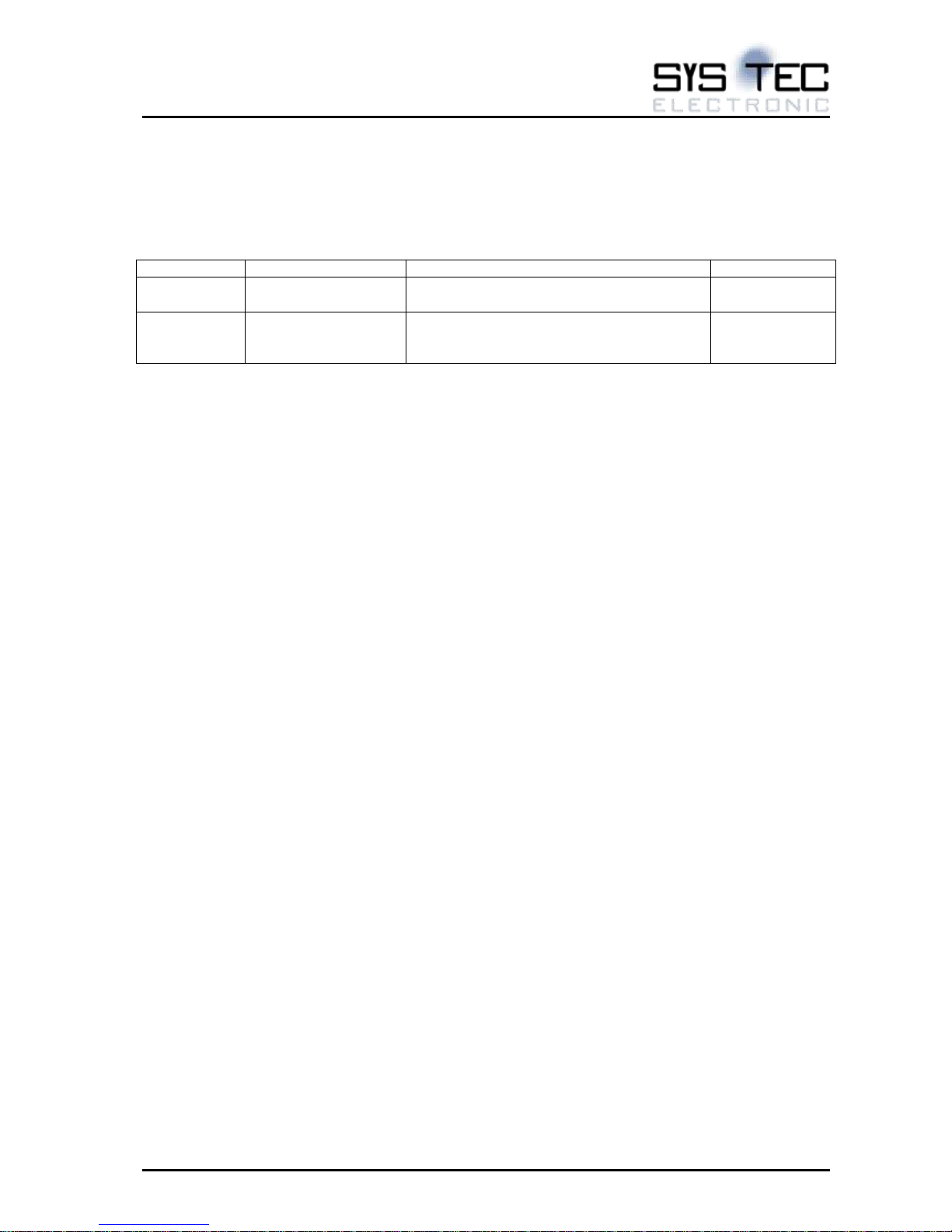
2.1 Orderable parts
Part number
Product name
Feature
Notes
4001046
ECUcore-1021 (1GB)
LS1021A, 1GB DDR3L, 128MB Flash, 40/+85°C
GPCM8/GASIC8
Support only
tbd
ECUcore-1021 (1GB)
LS1021A, 1GB DDR3L, 128MB Flash, 40/+85°C with support for GPCM with 16bit
multiplexed address/data bus Interface
SPI1 controller
is not available.
Table 1: Orderable parts
Options: Additional ECC-RAM and/or support for Profibus baud rate of 12MBaud on request.
Page 9

SYS TEC electronic GmbH
L-1589e-04 Hardware Manual ECUcore-1021
Page 9/30
Classification: Release
2.2 Technical Data
CPU core
Processor
NXP QorIQ LS1021A
- Dual-core Cortex-A7 (ARM® Cortex®-A7 MPCore
compliant with ARMv7-A™ architecture)
Each core includes:
– 32 Kbyte L1 Instruction Cache (ECC protection)
– 32 Kbyte L1 Data Cache (ECC protection)
– NEON co-processor
– Floating Point (FPU)
– QorIQ Trust Architecture and ARM TrustZone®
For both cores:
– 512 Kbyte unified I/D L2 Cache (ECC protection)
CPU Clock
1GHz each Core
Main memory
DDR3L-1600MT, 32bit + ECC (optional)
1GB (Optional 2GB)
Boot memory
Quad-SPI NOR-Flash
2x64MB
Mass storage
SATA
1x SATA3.0 controller
SD-Card
1x interface for SDHC/MMC/eMMC
Connectivity
Ethernet
Up to 3x GbE Ethernet (1x on-board GbE-Phy, up to
2x SGMII, 1x RGMII)
On-board Phy Feature:
- 10/100BASE-TX, 1000BASE-T
- Auto-MDI/MDI-X
- Auto-Negotiation
- Digital Loopback and Analog Remote Loopback
mode
- LinkMD Cable diagnostics
PCI Express
2x PCI Express Gen2 controllers
USB-Host
1x USB3.0 controller with integrated Phy
Page 10
SYS TEC electronic GmbH
L-1589e-04 Hardware Manual ECUcore-1021
Page 10/30
Classification: Release
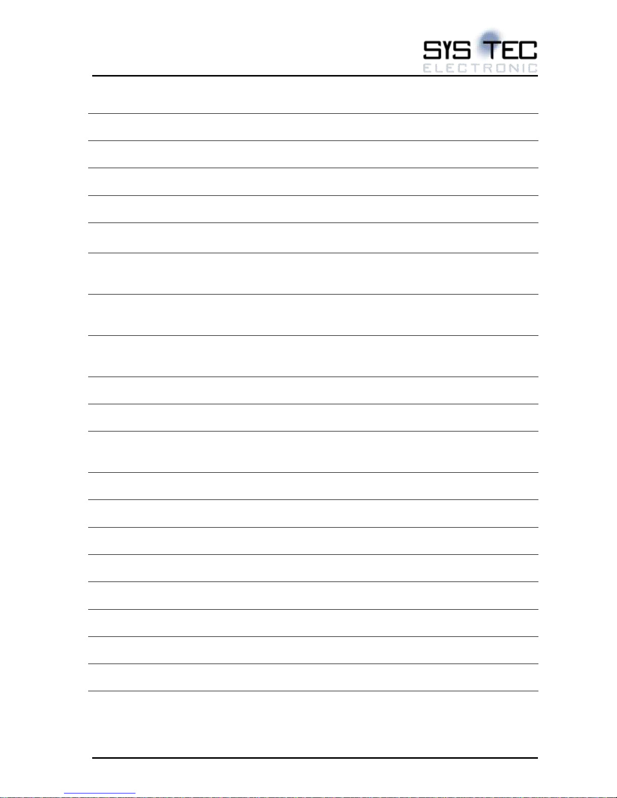
UART
Up to 2x DUART, up to 6x LPUART
CAN
Up to 4x FlexCAN modules
I2C
Up to 2x I2C controllers
SPI
Up to 2x SPI interfaces, 1 QSPI interface
Display
24-bit RGB, 12bit DDR pin interface
AUDIO
Up to 4 synchronous audio interfaces (I2S/SAI)
1 SPDIF
Temperature sensor
Measurement of CPU junction temperature
Measurement of board ambient temperature
Measurement range: -55°C … +150°C
Misc. peripherals
FlexTimer/PWM
GPIOs
Interrupt inputs
Real Time Clock (RTC)
Current consumption (sleep mode)
<1µA
RTC voltage buffer
External battery or capacitor
Power Supply
Main Power Supply of Module (DVDD, D1VDD)
3.3V±5%
Rise Time
Max. 1V/ms
Voltage ripple
33mV @0…20MHz
Power Consumption (full load)
Max. 4.5W
Internal power supply domains
BVDD, DVDD, D1VDD, EVDD, USB_HVDD
3.3V
LVDD, L1VDD
2.5V
OVDD, O1VDD
1.8V
Page 11
SYS TEC electronic GmbH
L-1589e-04 Hardware Manual ECUcore-1021
Page 11/30
Classification: Release
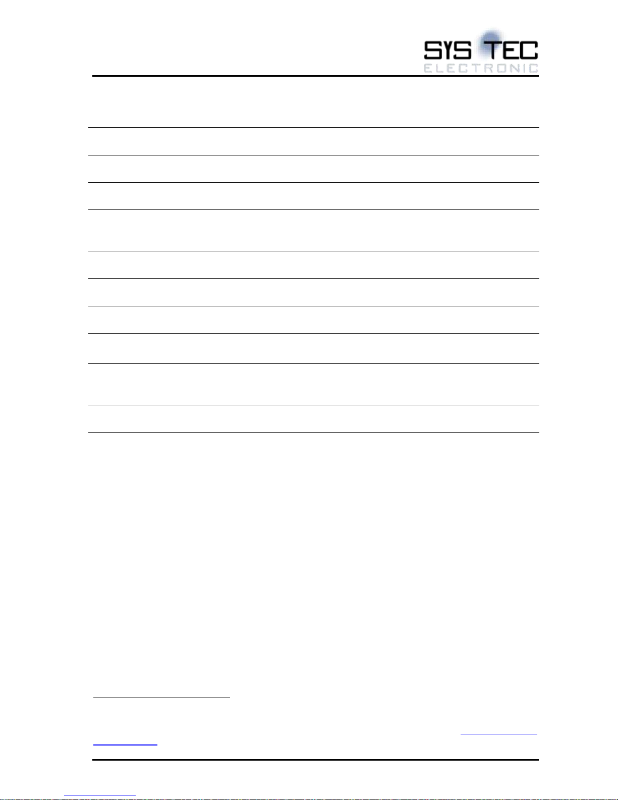
Temperature range
Operating
-40°C/+85°C1
Storage
-55/+125°C
Humidity
Operating
10% …90%
Storage
<95%
MTBF
> 650000h @ 40°C
(applied standard: Siemens SN 29500)
Mechanical dimension
Board size
84mm x 55mm
Table 2: Technical data
1
For the full operating temperature range is to ensure sufficient cooling. For the connection to a heat
sink, a heat spreader is available (see accessories on SYS TEC web page http://www.systec-
electronic.com/, see also sec. 3.14).
Page 12
SYS TEC electronic GmbH
L-1589e-04 Hardware Manual ECUcore-1021
Page 12/30
Classification: Release
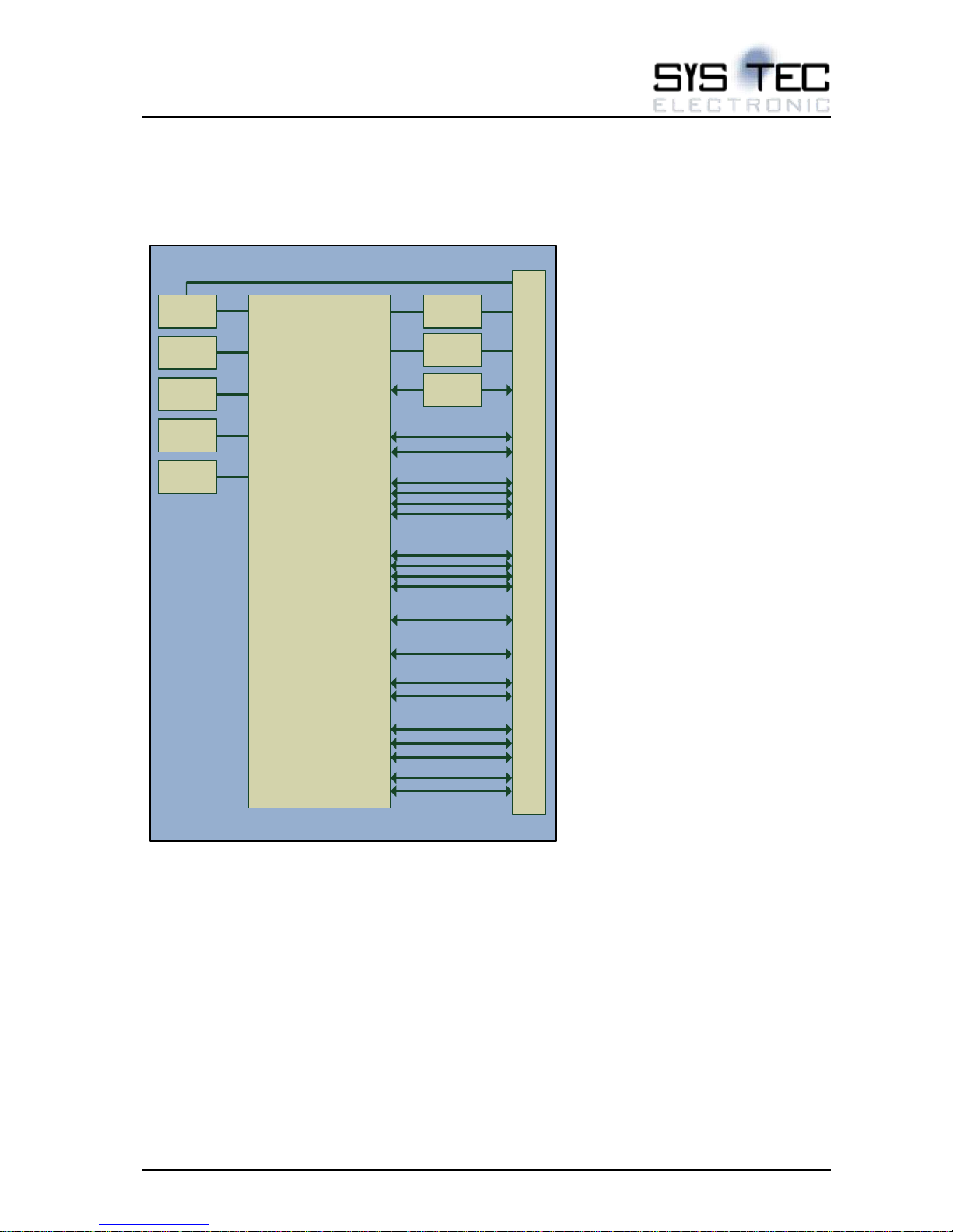
2.3 Block Diagram
The LS1021A signals are combined in signal groups. A signal group is selected using the RCW field
value. Some signal groups serve multiple functions multiplexed by RCW field.
ECUcore-1021
GbE0
DDR3
CLOCK
FLASH
°C
RTC
WATCH
DOG
GbE Phy
QorIQ LS1021A
SPI1
EC1
EC2
LANE A
LANE B
LANE C
LANE D
UART1
UART2
I2C1
TDMA
TDMB
QSPI_A
QSPI_B
USB1
SDHC
GPIOs
IRQ0,1,2
JTAG
RGMII/CAN1-2/SAI1,2/FTM1/GPIO
PCIe
SATA/SGMII
SGMII/PCIe/SATA
SGMII
UART2-4/LPUART1,2,4/SPI2
DISPLAY/GPIO/UCC1/SAI3/FTM4
DISPLAY/GPIO/UCC3/SPDIF/SAI4/FTM4
SDHC/I2C2/LPUART2,3,5,6/GPIO
USB3.0
IRQs
GPIO/IRQ
I2C
SPI
QSPI
Battery
RESET
Trigger IN/OUT
CAN3-4/FTM2/GPIO
UART1
Module conne ctor
3.3V
PMIC
Available Interfaces on Carrier Board:
TAMPER
TAMPER-Dete ction
Figure 1: Block diagram ECUcore-1021
Page 13
SYS TEC electronic GmbH
L-1589e-04 Hardware Manual ECUcore-1021
Page 13/30
Classification: Release
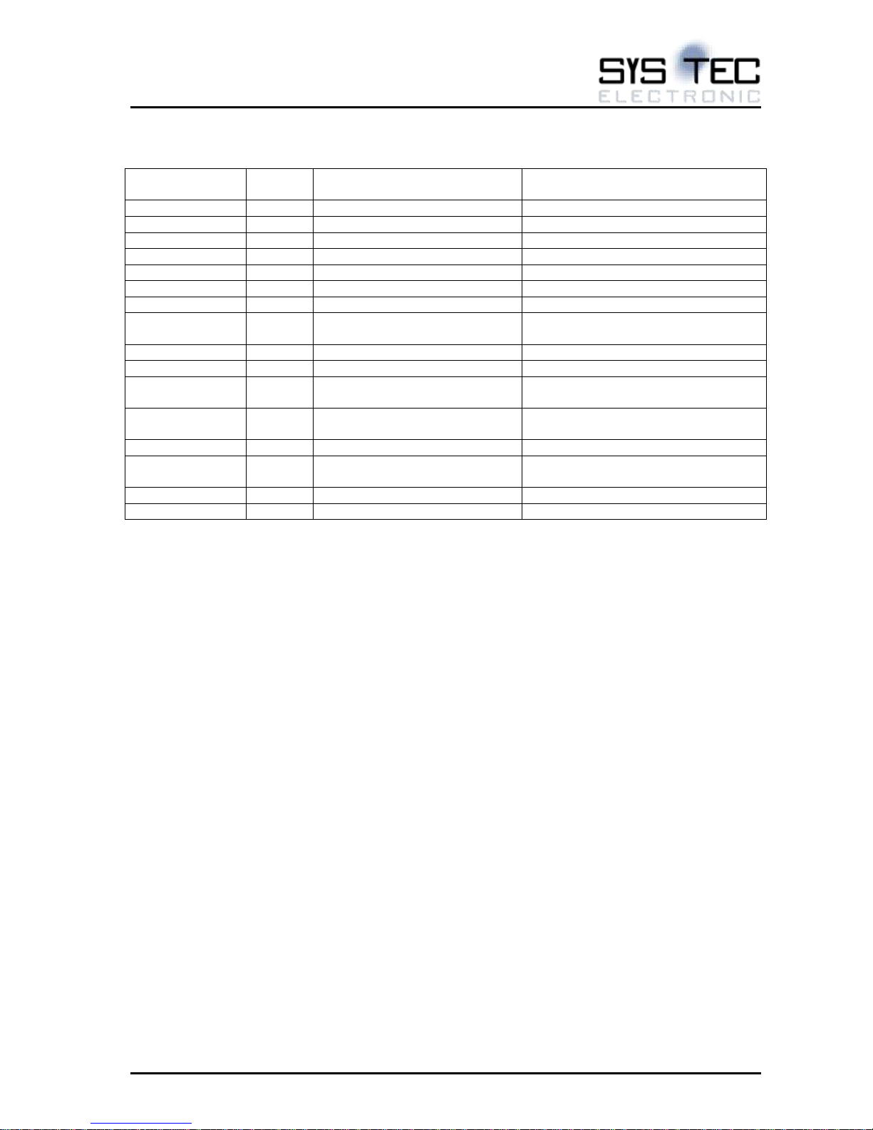
The following table shows the primary and the alternative signal functions for off-board usable signals.
Field Name from
LS1021A RM
Voltage
domain
Primary signal functions
(defined by SYS TEC BSP)
Alternative signal functions
(defined by Customer specific BSP)
EC1
2.5V
CAN1, CAN2
RGMII, GPIO3, SAI1, SAI2, FTM1
EC2
2.5V
CAN3, CAN4
GPIO3, FTM2
EC3
2.5V
RGMII3
-
MDC/MDIO
2.5V
EMI1
-
RTC
1.8V
RTC
GPIO1_14
ASLEEP
1.8V
ASLEEP
GPIO1_13
EVT[9]_B
1.8V
EVT[9]_B
GPIO2_24
UART_EXT,
UART_BASE
3.3V
UART1, LPUART1, 2D-ACE
(Display)
GPIO1, UART2, UART3, UART4,
LPUART2, LPUART4, SPI2
QE/TDMA
3.3V
2D-ACE (Display)
GPIO4, UC1, SAI3, FTM4
QE/TDMB
3.3V
2D-ACE (Display)
GPIO4, UC3, SPDIF, SAI4, FTM4
IIC_EXT,
IIC_BASE
3.3V
IIC1, SDHC
GPIO4, IIC2, SPI2
SDHC_EXT,
SDHC_BASE
3.3V
SDHC
GPIO2, LPUART2, LPUART3,
LPUART5, LPUART6
SDHC
3.3V
GPIO4_23-GPIO4_26
SDHC
IRQ_EXT,
IRQ_BASE
2.5V
3.3V
IRQ3
IRQ4, IRQ5
CLK9-12
3.3V
CLK9-12
GPIO4_19-GPIO4_22, BRG01-4
SPI1
3.3V
SPI1 signals
IFC pins
Table 3: Overview to primary and alternative signal functions of LS1021A signal groups
Page 14
SYS TEC electronic GmbH
L-1589e-04 Hardware Manual ECUcore-1021
Page 14/30
Classification: Release
2.4 Module connector and pin assignment
This chapter describes the module pin and connector configuration. The connector on the module side is
called receptacle, the connector on the Carrier board is called plug-in connector.
Note: The connectors are COMexpress compatible types. However, the pin assignment and the
connector arrangement meet not the COMexpress standard!
2.4.1 Connector type for the Carrier board
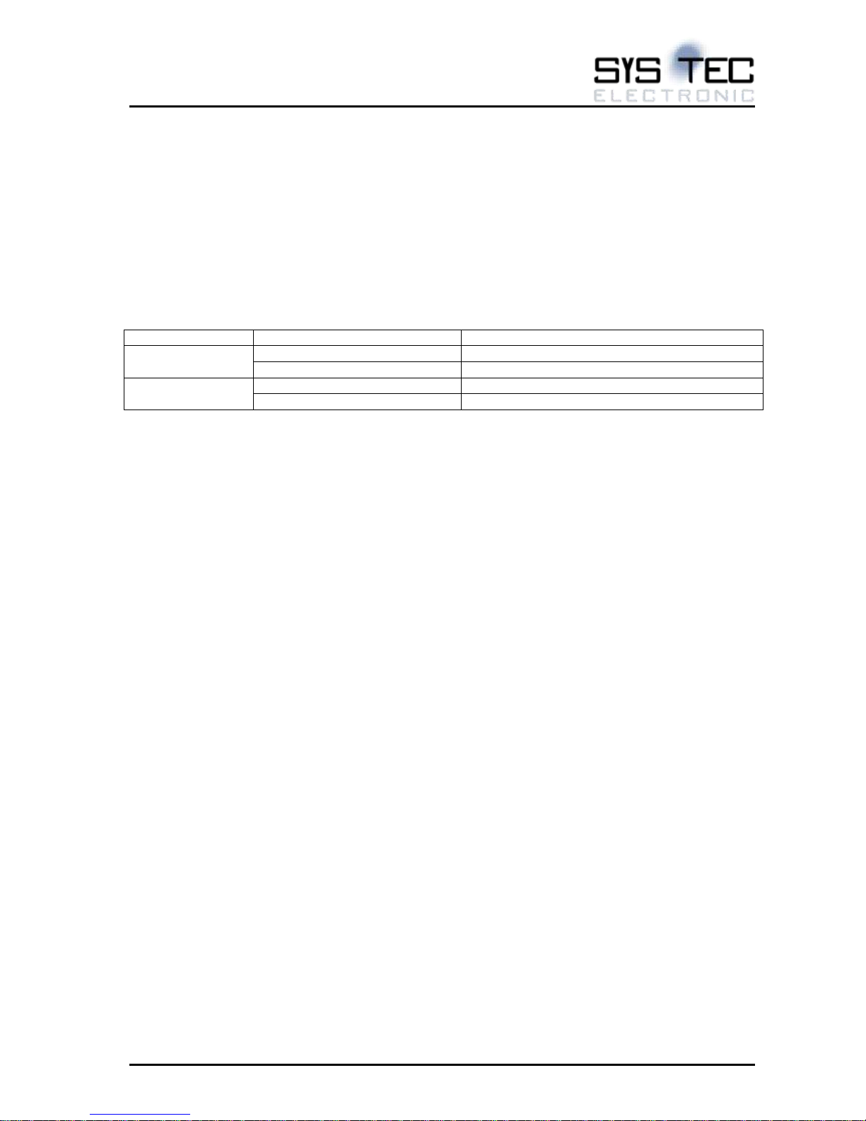
The Carrier board shall use a 5mm or 8mm heights 220pin plug-in connector:
Supplier
Board-to-board stack height
Order number of supplier
Tyco Electronics
5mm
3-1827253-6
8mm
3-6318491-6
Foxconn
5mm
QT002206-2131-3H
8mm
QT002206-4131-3H
Table 4: Carrier board plug-in connector
2.4.2 Pin assignment row A and row B
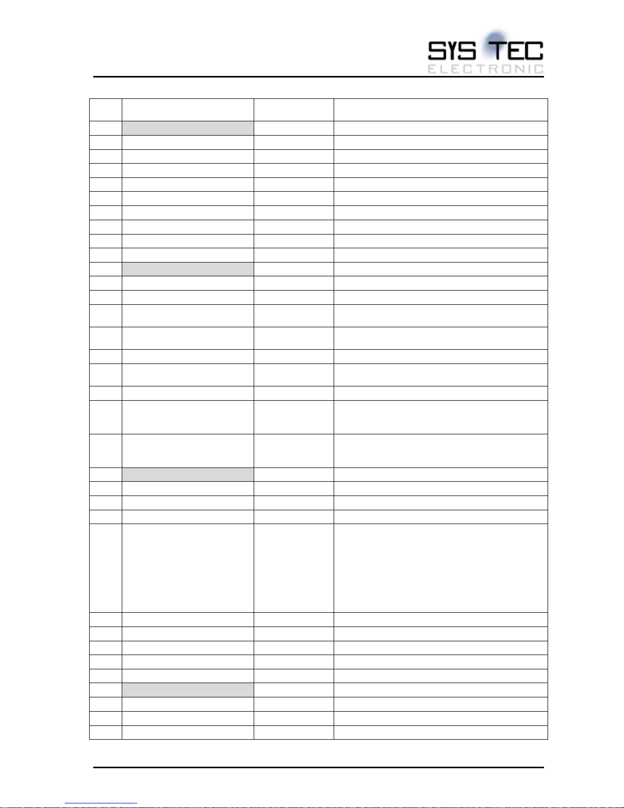
The pin name corresponds to the primary pin name of the LS1021A called by NXP, unless there is only
an alternative function available. In this case the pin name corresponds to the alternative function only.
For description of primary and alternative function see the NXP data sheets.
A pin configuration is defined by the Reset Configuration Word (RCW). The RCW is pre-installed
according to the ordered module variant (see chapter 2.1).
In contrast to the description in the NXP data sheet and Reference Manual, the active-low signals are
denoted by “/” (example: UART2_RTS_B (NXP manual) is denoted as UART2_/RTS).
The module has two primary power supply domains (DVDD, D1VDD) and several domains that are onboard generated (BVDD, EVDD, OVDD, O1VDD, ...). For every pin, the corresponding voltage domain is
specified. An internal pull-up resistor is connected to this voltage domain then. Signals that relates to
voltage domains lower than 3.3V are marked with the voltage value in the signal name.
For every pin, the recommendations of the manufacture must be noted. The information in the
data sheet of LS1021A must be observed.
Page 15
SYS TEC electronic GmbH
L-1589e-04 Hardware Manual ECUcore-1021
Page 15/30
Classification: Release
Pin
Name
Voltage
domain
Notes
A1
GND
-
A2
ASLEEP_1V8
O1VDD (1.8V)
Internal pull-up resistor (4.7kΩ)
A3
QSPI_DQS_B
BVDD (3.3V)
A4
QSPI_CK_B
BVDD (3.3V)
Note 1
A5
QSPI_/CS_B1
BVDD (3.3V)
A6
QSPI_/CS_B0
BVDD (3.3V)
A7
QSPI_DIO_B3
BVDD (3.3V)
A8
QSPI_DIO_B2 (IFC_/PERR)
BVDD (3.3V)
A9
QSPI_DIO_B1 (IFC_PAR1)
BVDD (3.3V)
A10
QSPI_DIO_B0 (IFC_PAR0)
BVDD (3.3V)
A11
GND
-
A12
IFC_CLK1
BVDD (3.3V)
A13
IFC_CLK0
BVDD (3.3V)
A14
IFC_/RB0
BVDD (3.3V)
This Pin has an internal pull-up resistor of
4.7kΩ.
A15
IFC_/WE0
BVDD (3.3V)
This Pin has an internal pull-down resistor of
4.7kΩ.
A16
IFC_CLE
BVDD (3.3V)
A17
IFC_/OE
BVDD (3.3V)
Pin must NOT be pulled down during power-on
reset.
A18
IFC_BCTL
BVDD (3.3V)
Pin is actively driven during reset.
A19
IFC_AVD
BVDD (3.3V)
Pin must NOT be pulled down during power-on
reset. This Pin has an internal pull-up resistor of
4.7kΩ.
A20
SPI1_SIN (IFC_AD15)
BVDD (3.3V)
Optionally, this pin can be configured as
IFC_AD15 signal on request (assembly variant,
see ).
A21
GND
-
A22
SPI1_SCK
BVDD (3.3V)
A23
SPI1_PCS0 (IFC_/CS1)
BVDD (3.3V)
A24
IFC_/CS0
BVDD (3.3V)
Note 1
A25
IFC_AD14
BVDD (3.3V)
Select Boot device:
1 = QSPI-Flash is Boot device (Default)
0 = SD-Card is Boot device
This pin is a reset configuration pin and has an
internal pull-up resistor of 10kΩ. According to
the external pin configuration see also Note 1.
A26
SPI1_SOUT (IFC_AD13)
BVDD (3.3V)
Note 2
A27
SPI1_PCS5 (IFC_AD12)
BVDD (3.3V)
Note 2
A28
SPI1_PCS4 (IFC_AD11)
BVDD (3.3V)
Note 2
A29
SPI1_PCS3 (IFC_AD10)
BVDD (3.3V)
Note 1
A30
SPI1_PCS2 (IFC_AD9)
BVDD (3.3V)
Note 2
A31
GND
-
A32
SPI1_PCS1 (IFC_AD8)
BVDD (3.3V)
Note 2
A33
IFC_AD7
BVDD (3.3V)
A34
IFC_AD6
BVDD (3.3V)
Page 16
SYS TEC electronic GmbH
L-1589e-04 Hardware Manual ECUcore-1021
Page 16/30
Classification: Release
Pin
Name
Voltage
domain
Notes
A35
IFC_AD5
BVDD (3.3V)
A36
IFC_AD4
BVDD (3.3V)
A37
IFC_AD3
BVDD (3.3V)
A38
IFC_AD2
BVDD (3.3V)
A39
IFC_AD1
BVDD (3.3V)
A40
IFC_AD0
BVDD (3.3V)
A41
GND
- A42
USB1_TX_P
-
A43
USB1_TX_M
-
A44
USB1_RX_P
- A45
USB1_RX_M
- A46
USB1_DP
- A47
USB1_DM
-
A48
USB1_VBUS
USB_VBUS
See CPU datasheet for interface
recommendation
A49
GPIO4_26
DVDD (3.3V)
A50
GPIO4_25
DVDD (3.3V)
A51
GND
-
A52
GPIO4_24
DVDD (3.3V)
A53
GPIO4_23
DVDD (3.3V)
A54
SDHC_DAT3
EVDD (3.3V)
A55
SDHC_DAT2
EVDD (3.3V)
A56
SDHC_DAT1
EVDD (3.3V)
A57
SDHC_DAT0
EVDD (3.3V)
A58
SDHC_CLK
EVDD (3.3V)
A59
SDHC_CMD
EVDD (3.3V)
A60
GND
-
A61
SDHC_WP/I2C2_SDA
DVDD (3.3V)
If configured as I2C interface signal this pin is
an open-drain signal and a pull-up resistor of
1kΩ should be placed on this pin to 3V3.
A62
SDHC_/CD/I2C2_SCL
DVDD (3.3V)
If configured as I2C interface signal this pin is
an open-drain signal and a pull-up resistor of
1kΩ should be placed on this pin to 3V3.
A63
VBAT
-
On-board RTC power supply pin (2.0V … 3.6V)
A64
RTC_1V8
OVDD (1.8V)
Internal pull-down resistor (10kΩ)
A65
TA_BB_RTC_1V0
TA_BB_VDD
(1.0V)
Internal pull-down resistor (10kΩ)
A66
/TA_TD_1V8
OVDD (1.8V)
Tamper Detect input TA_TMP_DETECT_B
(Internal pull-up resistor of 1kΩ)
A67
/TA_BB_TD_1V0
TA_BB_VDD
(1.0V)
Low Power Tamper Detect
(TA_BB_TMP_DETECT_B) (Internal pull-up
resistor of 1kΩ)
A68
/TEST_SEL_1V8
O1VDD (1.8V)
Internal pull-up resistor (1kΩ)
A69
THERM_/CRIT
DVDD (3.3V)
Open-drain output of CPU temperature sensor
to signal critical temperature values (Internal
pull-up resistor (4.7kΩ) to 3.3V), see chap. 3.11
A70
GND
- A71
/EVT3_1V8
O1VDD (1.8V)
Internal pull-up resistor of 10kΩ
A72
/EVT4_1V8
O1VDD (1.8V)
Internal pull-up resistor of 10kΩ
Page 17
SYS TEC electronic GmbH
L-1589e-04 Hardware Manual ECUcore-1021
Page 17/30
Classification: Release
Pin
Name
Voltage
domain
Notes
A73
CLK2_25M_3V3
DVDD (3.3V)
25MHz Reference clock for external devices
A74
GND
- A75
SD1_RX3_P
-
SERDES Lane D Receive data (positive)
A76
SD1_RX3_N
-
SERDES Lane D Receive data (negative)
A77
GND
- A78
SD1_TX3_P
-
SERDES Lane D Transmit data (positive)
A79
SD1_TX3_N
-
SERDES Lane D Transmit data (negative)
A80
GND
-
A81
SD1_CLK0_P
-
PCIe 100MHz Reference clock (positive)
A82
SD1_CLK0_N
-
PCIe 100MHz Reference clock (negative)
A83
GND
- A84
SD1_RX0_P
-
SERDES Lane A Receive data (positive)
A85
SD1_RX0_N
-
SERDES Lane A Receive data (negative)
A86
GND
- A87
SD1_TX0_P
-
SERDES Lane A Transmit data (positive)
A88
SD1_TX0_N
-
SERDES Lane A Transmit data (negative)
A89
3V3
DVDD
Module power supply input (switchable) DVDD
A90
GND
- A91
UART2_TX
D1VDD (3.3V)
Signal UART2_SOUT of LS1021A
A92
UART2_RX
D1VDD (3.3V)
Signal UART2_SIN of LS1021A
A93
UART2_/RTS
D1VDD (3.3V)
A94
UART2_/CTS
D1VDD (3.3V)
A95
UART1_RX
DVDD (3.3V)
Signal UART1_SIN of LS1021A
A96
UART1_TX
DVDD (3.3V)
Signal UART1_SOUT of LS1021A
A97
UART1_/RTS
DVDD (3.3V)
A98
UART1_/CTS
DVDD (3.3V)
A99
CLK11
DVDD (3.3V)
This Pin has an internal series resistor of 33Ω.
A100
GND
- A101
CLK12
DVDD (3.3V)
This Pin has an internal series resistor of 33Ω.
A102
/MR
D1VDD (3.3V)
low-active Manual RESET input (internal pull-up
resistor of 10kΩ)
A103
/PORST
D1VDD (3.3V)
Open-drain RESET output of PMIC with internal
pull-up resistor of 10kΩ
A104
/HRESET_1V8
O1VDD (1.8V)
This pin has an internal pull-up resistor of 1kΩ.
A105
/RESET_REQ_1V8
O1VDD (1.8V)
This pin has an internal pull-up resistor of 1kΩ.
A106
3V3_D1VDD
D1VDD
Module power supply input (always on) D1VDD
A107
3V3_D1VDD
D1VDD
Module power supply input (always on) D1VDD
A108
3V3_D1VDD
D1VDD
Module power supply input (always on) D1VDD
A109
3V3_D1VDD
D1VDD
Module power supply input (always on) D1VDD
A110
GND
-
Table 5: Connector pin assignment (row A)
Page 18
SYS TEC electronic GmbH
L-1589e-04 Hardware Manual ECUcore-1021
Page 18/30
Classification: Release
Pin
Name
Voltage domain
Notes
B1
GND
-
B2
I2C1_SCL
D1VDD (3.3V)
Signal IIC1_SCL of LS1021A (open-drain) with
internal pull-up resistor of 7.5kΩ
B3
I2C1_SDA
D1DVDD (3.3V)
Signal IIC1_SDA of LS1021A (open-drain) with
internal pull-up resistor of 7.5kΩ
B4
SDC_SWD_CLK
DVDD (3.3V)
Reserved (Internal pull-down resistor of 10kΩ)
B5
SDC_SWD_DIO
DVDD (3.3V)
Reserved (Internal pull-up resistor of 10kΩ)
B6
SDC_/BOOT
DVDD (3.3V)
Reserved (Internal pull-up resistor of 4.7kΩ)
B7
SDC_/RESET
DVDD (3.3V)
Reserved (Internal pull-up resistor of 4.7kΩ)
B8
WDTI
DVDD (3.3V)
Watchdog trigger input (floating to disable watchdog)
B9
WDTO
DVDD (3.3V)
Watchdog output
B10
SDC_ADC0
-
Reserved (SDC analog Input ADC0)
B11
GND
-
B12
SDC_CLKOUT
DVDD (3.3V)
Reserved (RTC clockout)
B13
/IRQ0_1V8
O1VDD (1.8V)
Internal pull-up resistor of 1kΩ
B14
/IRQ1_1V8
OVDD (1.8V)
Internal pull-up resistor of 1kΩ
This pin is connected internal to the PMIC interrupt
output (open-drain).
B15
/IRQ2_2V5
L1VDD (2.5V)
Internal pull-up resistor of 4.7kΩ
B16
/IRQ3_2V5
LVDD (2.5V)
Internal pull-up resistor of 4.7kΩ
This pin is connected internal to the Ethernet Phy
interrupt output (open-drain).
B17
/IRQ4_3V3
DVDD (3.3V)
Internal pull-up resistor of 4.7kΩ
This pin is connected internal to the SDC interrupt
output (optional, open-drain) and Temperature
sensor interrupt output (open-drain).
B18
/IRQ5_3V3
DVDD (3.3V)
Internal pull-up resistor of 4.7kΩ
B19
/EVT9_1V8
O1VDD (1.8V)
Internal pull-up resistor of 10kΩ
B20
IFC_TE
BVDD (3.3V)
B21
GND
-
B22
EC1_TXD0
L1VDD (2.5V)
B23
EC1_TXD1
L1VDD (2.5V)
B24
EC1_TXD2
L1VDD (2.5V)
B25
EC1_TXD3
L1VDD (2.5V)
B26
EC1_RX_DV
L1VDD (2.5V)
B27
EC1_RXD0
L1VDD (2.5V)
B28
EC1_RXD1
L1VDD (2.5V)
B29
EC1_RXD2
L1VDD (2.5V)
B30
EC1_RXD3
L1VDD (2.5V)
B31
GND
-
B32
EC1_RX_CLK
L1VDD (2.5V)
B33
EC1_GTX_CLK
L1VDD (2.5V)
B34
EC1_GTX_CLK125
L1VDD (2.5V)
B35
EC1_TX_EN
L1VDD (2.5V)
B36
CLK3_25M_2V5
LVDD (2.5V)
B37
EMI1_MDC
L1VDD (2.5V)
Internal pull-up resistor of 4.7kΩ
B38
EMI1_MDIO
L1VDD (2.5V)
Internal pull-up resistor of 4.7kΩ
B39
EC2_RX_CLK
LVDD (2.5V)
Page 19
SYS TEC electronic GmbH
L-1589e-04 Hardware Manual ECUcore-1021
Page 19/30
Classification: Release
Pin
Name
Voltage domain
Notes
B40
EC2_TX_EN
LVDD (2.5V)
B41
GND
-
B42
EC2_RX_DV
LVDD (2.5V)
B43
EC2_TXD0
LVDD (2.5V)
B44
EC2_TXD1
LVDD (2.5V)
B45
EC2_TXD2
LVDD (2.5V)
B46
EC2_TXD3
LVDD (2.5V)
B47
EC2_RXD0
LVDD (2.5V)
B48
EC2_RXD1
LVDD (2.5V)
B49
EC2_RXD2
LVDD (2.5V)
B50
EC2_RXD3
LVDD (2.5V)
B51
GND
-
B52
GBE0_D-
-
Gigabit Ethernet Interface 0:
MDI[3]-, negative signal of differential pair
B53
GBE0_D+
-
Gigabit Ethernet Interface 0:
MDI[3]+, positive signal of differential pair
B54
GBE0_C-
-
Gigabit Ethernet Interface 0:
MDI[2]-, negative signal of differential pair
B55
GBE0_C+
-
Gigabit Ethernet Interface 0:
MDI[2]+, positive signal of differential pair
B56
GBE0_B-
-
Gigabit Ethernet Interface 0:
MDI[1]-, negative signal of differential pair
B57
GBE0_B+
-
Gigabit Ethernet Interface 0:
MDI[1]+, positive signal of differential pair
B58
GBE0_A-
-
Gigabit Ethernet Interface 0:
MDI[0]-, negative signal of differential pair
B59
GBE0_A+
-
Gigabit Ethernet Interface 0:
MDI[0]+, positive signal of differential pair
B60
GND
-
B61
GBE0_LED2
Gigabit Ethernet Interface 0: LINK LED (Green)
LINK off: GBE0_LED2 = H => LED OFF
LINK on: GBE0_LED2 = L => LED ON
Note: Internal pull-down resistor of 1kΩ.
B62
GBE0_LED1
Gigabit Ethernet Interface 0: ACTIVITY LED (Yellow)
No Activity: GBE0_LED1 = H => LED OFF
Activity (Rx, Tx): GBE0_LED1 = Toggle => LED
Blinking
Note: Internal pull-up resistor of 10kΩ.
B63
JTAG_VREF_1V8
OVDD (1.8V)
Reference voltage of 1.8V for JTAG interface
(Internal series resistor of 270Ω)
B64
JTAG_/RESET
OVDD (1.8V)
This signal triggers the /PORESET signal of
LS1021A during boundary scan test session.
B65
JTAG_TMS
OVDD (1.8V)
Signal TMS of LS1021A
B66
JTAG_TCK
OVDD (1.8V)
Signal TCK of LS1021A (Internal pull-up of 10kΩ)
B67
JTAG_TDO
OVDD (1.8V)
Signal TDO of LS1021A
B68
JTAG_TDI
OVDD (1.8V)
Signal TDI of LS1021A
B69
/EVT0_1V8
O1VDD (1.8V)
Internal pull-up resistor of 10kΩ
B70
GND
-
B71
/EVT1_1V8
O1VDD (1.8V)
Internal pull-up resistor of 10kΩ
B72
/EVT2_1V8
O1VDD (1.8V)
Internal pull-up resistor of 10kΩ
Page 20
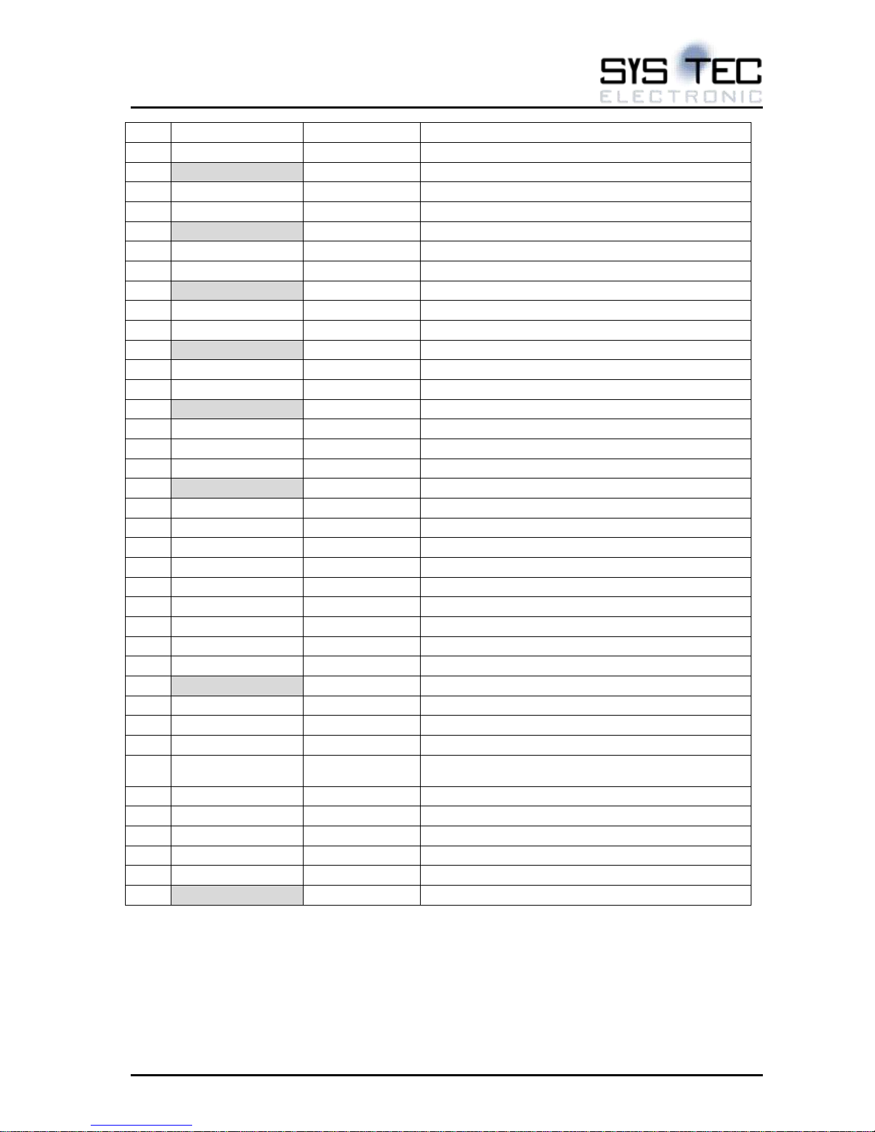
SYS TEC electronic GmbH
L-1589e-04 Hardware Manual ECUcore-1021
Page 20/30
Classification: Release
Pin
Name
Voltage domain
Notes
B73
CLK1_25M_3V3
DVDD (3.3V)
B74
GND
-
B75
SD1_RX1_N
-
SERDES Lane B Receive data (negative)
B76
SD1_RX1_P
-
SERDES Lane B Receive data (positive)
B77
GND
-
B78
SD1_TX1_N
-
SERDES Lane B Transmit data (negative)
B79
SD1_TX1_P
-
SERDES Lane B Transmit data (positive)
B80
GND
-
B81
SD1_CLK2_N
PCIe 100MHz Reference clock (negative)
B82
SD1_CLK2_P
PCIe 100MHz Reference clock (positive)
B83
GND
-
B84
SD1_RX2_N
SERDES Lane C Receive data (negative)
B85
SD1_RX2_P
SERDES Lane C Receive data (positive)
B86
GND
-
B87
SD1_TX2_N
SERDES Lane C Transmit data (negative)
B88
SD1_TX2_P
SERDES Lane C Transmit data (positive)
B89
3V3
DVDD
Module power supply input (switchable) DVDD
B90
GND
-
B91
CLK10
DVDD (3.3V)
This Pin has an internal series resistor of 33Ω.
B92
CLK09
DVDD (3.3V)
This Pin has an internal series resistor of 33Ω.
B93
TDMB_RQ
DVDD (3.3V)
This Pin has an internal series resistor of 33Ω.
B94
TDMB_TSYNC
DVDD (3.3V)
This Pin has an internal series resistor of 33Ω.
B95
TDMB_TXD
DVDD (3.3V)
This Pin has an internal series resistor of 33Ω.
B96
TDMB_RSYNC
DVDD (3.3V)
This Pin has an internal series resistor of 33Ω.
B97
TDMB_RXD
DVDD (3.3V)
This Pin has an internal series resistor of 33Ω.
B98
TDMA_RQ
DVDD (3.3V)
This Pin has an internal series resistor of 33Ω.
B99
TDMA_TSYNC
DVDD (3.3V)
This Pin has an internal series resistor of 33Ω.
B100
GND
-
B101
TDMA_TXD
DVDD (3.3V)
This Pin has an internal series resistor of 33Ω.
B102
TDMA_RSYNC
DVDD (3.3V)
This Pin has an internal series resistor of 33Ω.
B103
TDMA_RXD
DVDD (3.3V)
This Pin has an internal series resistor of 33Ω.
B104
2V5_LVDD
LVDD
Power supply output 2.5V to supply external level
shifter
B105
3V3
DVDD
Module power supply input (switchable) DVDD
B106
3V3_D1VDD
D1VDD
Module power supply input (always on) D1VDD
B107
3V3_D1VDD
D1VDD
Module power supply input (always on) D1VDD
B108
3V3_D1VDD
D1VDD
Module power supply input (always on) D1VDD
B109
3V3_D1VDD
D1VDD
Module power supply input (always on) D1VDD
B110
GND
-
Table 6: Connector pin assignment (row B)
Note 1: This pin is a reset configuration pin and has an internal pull-up resistor of 4.7kOhm. The signal
must be high after reset. If there is any device on the net of customer carrier board that might pull down
the value of the net at reset, a pull-up or active driver is needed.
Note 2: This pin is a reset configuration pin and has an internal pull-down resistor of 1kOhm. The signal
must be low after reset. If there is any device on the net of customer carrier board that might pull up the
value of the net at reset, a pull-down or active driver is needed.
Page 21
SYS TEC electronic GmbH
L-1589e-04 Hardware Manual ECUcore-1021
Page 21/30
Classification: Release
2.5 Mechanical Dimensions and Heat spreader
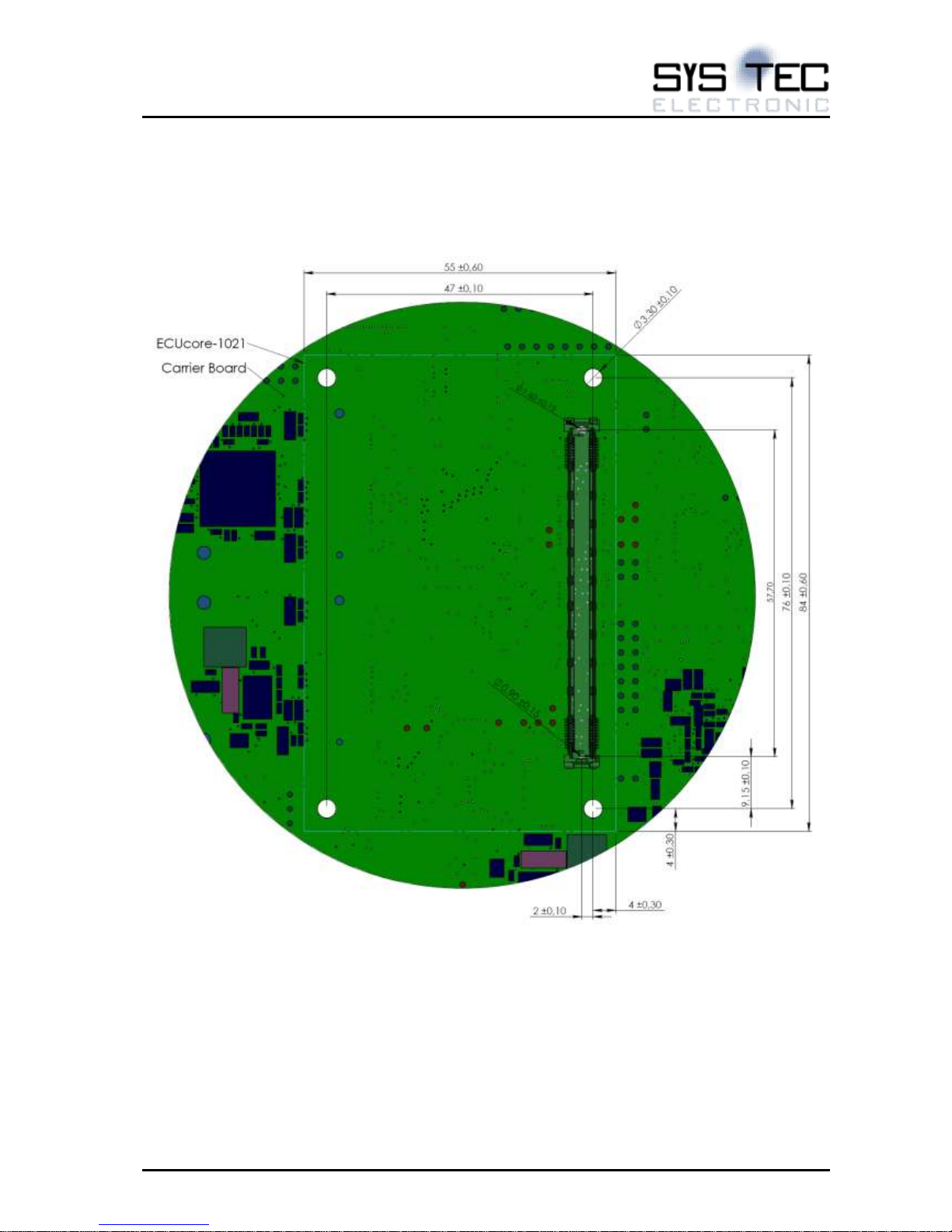
Figure 2 shows the dimension of the module as well as the location of the connector on the Carrier Board.
Please note that this is a view of the Carrier Board through the Module.
Figure 2: Module dimension and location of Module connector on Carrier Board
Page 22
SYS TEC electronic GmbH
L-1589e-04 Hardware Manual ECUcore-1021
Page 22/30
Classification: Release
It is important that the PCB drill tolerances of fixing holes for the plug-in connector meets the
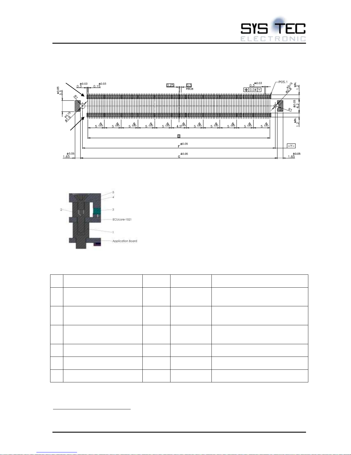
recommended ranges of manufacture data sheet.
Figure 3: Carrier board plug-in connector physical dimension2
The Figure 4 shows the use of stand-offs for mounting the
Module and the heat spreader. The heat spreader is thermally
coupled to the Module via thermal gap filler. The heat spreader
acts as thermal interface between the Module and the application
specific thermal solution. The heat spreader should be connected
to GND on the Carrier Board to improve EMC performance.
Figure 4: Mounting example of Module, Carrier Board and heat spreader
No
Component
Quantity
Order
number
Comments
1
Standoffs for 5mm board-toboard distance, solder mode,
M2.5
4
EFCO
ECM00530-L
Soldered on Carrier Board
1
Standoffs for 8mm board-toboard distance, solder mode,
M2.5
4
EFCO
ECM00579-L
Soldered on Carrier Board
2
Standoffs M2.5 x 5mm
4
SYS TEC
178185
To mounting the Module to the
Carrier Board and define the distance
to the heat spreader
3
Thermally gap filler
81mmx40mm, 2mm thick
1
SYS TEC
178264
Thermally gap filler between Module
and heat spreader
4
Heat spreader ECUcore-1021,
5mm thick
1
SYS TEC
178263
5 Countersunk screw with cross
recess M2.5 x 5mm
4
SYS TEC
175069
To mounting the heat spreader to the
standoffs and Module
Table 7: Mechanical mounting material
2
Source: Tyco electronics data sheet 3-1827253-6
row A
row B
Page 23
SYS TEC electronic GmbH
L-1589e-04 Hardware Manual ECUcore-1021
Page 23/30
Classification: Release
3 Design-in Considerations
3.1 Power Supply Design considerations
This section provides design recommendations for the power supply of ECUcore-1021. For information
about module power supply values and power consumption see Table 2.
The ECUcore-1021 is powered by a single power rail (see Table 2). The power supply inputs are 3V3 and
3V3_D1VDD. The 3V3_D1VDD-input is an always-on rails instead the 3V3 input, which can be switchedoff during Deep Sleep Mode (DSM). Some of the on-board components are supplied from input rails
directly. So the power supply rail must be met closely the requirements of product specification.
The signal levels of the module interface depend on the configured interface type. The carrier board
designer must note this fact if he connects the peripherals to the module. Otherwise, it may be
overloaded or destructed. See sec. 2.4 for more information of signal levels.
The module supply should be slew rate limited to no more as 2.5mV/ms.
The on-board processor needs different power rails to support the configurable interfaces. Following
power rail configuration is used:
Power rails
Value
Applied interfaces
BVDD
3.3V
QSPI, SPI1, IFC, FTM5, FTM6, FTM7, I2C, GPIO3
EVDD
3.3V
GPIO2, eSDHC, LPUART3, 5, 6
D1VDD,
DVDD
3.3V
DUART, I2C, DMA, QE, TDM, 2D-ACE, LPUART1, 2, 4, GPIO1, eSDHC,
SAI(I2S) 3, 4, SPDIF, FTM4, FTM8, SPI2, IRQ
LVDD,
L1VDD
2.5V
EC1, EC2, EC3, EMI1, GPIO1, GPIO3, CAN1-4, FTM1-3, SAI (I2S)1-2
Table 8: Overview of configured on-board power rails
3.2 Power-on RESET and RESET Configurations
After power supply is applied to the module and all internal power rails reach the required output value
the signal /PORST is de-asserted after 140ms – 280ms. After the rising edge of /PORST the reset control
logic of LS1021A begins cycling the device through its full reset and RCW configuration process. Note the
recommendation in Table 5 and Table 6 to read the right RCW value from the input pins.
3.3 Manual RESET (/MR)
A reset occurs if the manual reset (/MR) is switched to GND. The signal input must be driven by an opendrain output or can be connected with an RESET button. The signal input has an internal pull-up resistor.
3.4 System Booting
The Module supports the on-board QSPI NOR-Flash memory or a device connected to the eSDHC
interface of module. The boot device is selected by the pre-boot loader of LS1021A via pin IFC_AD14. If
IFC_AD14 is set to low during a power cycle, the pre-boot loader selects the eSDHC as boot device
interface instead of on-board QSPI NOR-Flash. The pre-boot loader of LS1021A performs configuration
register reads and writes to initialize the boot device interface, loads the RCW and pre-boot initialization
commands form the boot device, and writes data to configuration registers before the local cores of
LS1021A are permitted to boot.
3.5 General interface design consideration
For design-in of standard interfaces like PCIe2.0, Ethernet, SGMII, SATA3.0 or USB3.0 the rules of high
speed design should be noted. Important parameters are the signal line impedance, the signal line length,
Page 24
SYS TEC electronic GmbH
L-1589e-04 Hardware Manual ECUcore-1021
Page 24/30
Classification: Release
the layer stacking of the printed circuit board and the rules for design the signal traces on the board. The
trace width and spacing between the lines depend on the layer stacking. A good guidance for the highspeed interface design on the carrier board can be found in /3/. Additionally, the design-in and layout
recommendation of the chip vendors must be pay attention.
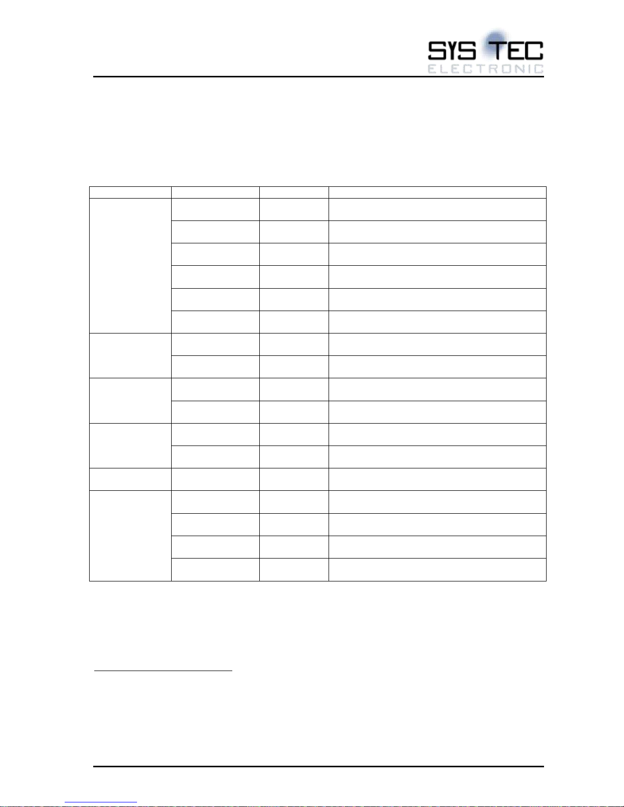
The following table shows the trace length used on the module. These lengths are taken into account in
design of the overall length (Carrier Board and Module).
Interface
Signals
Trace length
AC coupled on Module
PCIe 2.0
SD1_TX0_P
SD1_TX0_N
75mm
Yes
SD1_RX0_P
SD1_RX0_N
67mm
-
SD1_CLK0_P
SD1_CLK0_N
53mm
-
SD1_TX2_P
SD1_TX2_N
77mm
Yes
SD1_RX2_P
SD1_RX2_N
82mm
-
SD1_CLK2_P
SD1_CLK2_N
34mm
-
SGMII/SATA3.03
SD1_TX1_P
SD1_TX1_N
72mm
Yes
SD1_RX1_P
SD1_RX1_N
61mm
-
SGMII
SD1_TX3_P
SD1_TX3_N
98mm
Yes
SD1_RX3_P
SD1_RX3_N
113mm
-
USB3.0
USB1_TX_P
USB1_TX_N
36mm
Yes4
USB1_RX_P
USB1_RX_N
36mm
-
USB2.0
USB1_DP
USB1_DM
36mm
-
GbE
GBE0_A+
GBE0_A-
3.3mm
-
GBE0_B+
GBE0_B-
3.1mm
-
GBE0_C+
GBE0_C-
3.1mm
-
GBE0_D+
GBE0_D-
3.3mm
-
Table 9: High-speed interface trace lengths
3
The signal line length on Module meets not the recommendations in /3/. Therefore the maximum signal
line length on PCB (Module and Carrier Board) should be met the requirements (5.0 inches/127mm) in
/3/.
4
Until PCB revision 4377.0, the AC coupling capacitors are not support. The capacitors have to be
mounted on Carrier Board. Since PCB revision 4377.1, the capacitors are already present on the
ECUcore-module.
Page 25
SYS TEC electronic GmbH
L-1589e-04 Hardware Manual ECUcore-1021
Page 25/30
Classification: Release
3.6 PCI Express
The module supports two PCIe2.0 interfaces. For each interface a 100MHz reference clock output is
available. No additional clock buffer on carrier board is needed. The design-in information in /3/ should be
noted.
3.7 SGMII
The module supports up to two SGMII interfaces to connect GBE Phy’s. The SGMII interface needs no
reference clock. The 25MHz clock for the Phy can be derived from module clock outputs
(CLK1_25M_3V3). The design-in information of the Phy vendor should be noted.
3.8 SGMII/SATA
SGMII and SATA3.0 share the same SERDES-Lanes of LS1021A. SATA3.0 requires AC coupling
capacitors of 12nF directly at the SATA connector for RX and TX signal lines. In /3/ this would have
provided on the modules.
SGMII requires for the RX and TX signal lines an AC coupling capacitor of 100nF at the input side of the
Phy. The SGMII and the SATA requirements are contrary to /3/. For this reason, the specific AC coupling
capacitors must be located on the Carrier Board.
3.9 ETHERNET Interface considerations
The module provides one Ethernet port (GbE0) with integrated Phy (Additionally, up to two more
interfaces can be supported with SGMII-Phy’s on the Carrier Board). The interface supports 4 wire
10/100BASE-Tx and 8 wire 1000BASE-T as well. The interface signals can be used to connect to LAN
connector with internal or external isolation magnetics on the Carrier Board. Additionally to the
recommendations in /3/ for the connections of the magnetics to the Phy the following should be notes:
- Termination resistors required by the module Phy are present on the Module.
- The magnetic center tab must be terminated with a 100nF/±10% capacitance to ground. There is no
center tab reference signal on the Module connector.
- The module Phy provides two LED output pins (see Table 6). Each LED output pin can directly drive an
LED with a series resistor of typically 220Ω to 470Ω at 3.3V.
SYS TEC has acquired a pool of MAC addresses. The MAC address for the first Ethernet interface GbE0
is barcode-labelled and attached on the Module.
3.10 I2C Interface considerations
The I2C bus is a two-wire serial bus. The LS1021A supports up to three interfaces of I2C. The I2C1
interface is always available the other interfaces can also be occupied with an alternative function
depending on RCW.
Both signal lines (I2Cn_SCL, I2Cn_DAT) are driven by open-drain outputs of LS1021A. Each signal line
needs an external pull-up resistor (see Table 5 and Table 6 for the related power domain). Some
interfaces have a pull-up resistor on the ECUcore-1021. The carrier board should contain an additional
pull-up resistor. The line capacitance must not exceed the maximum allowed value. For a rule of thumb,
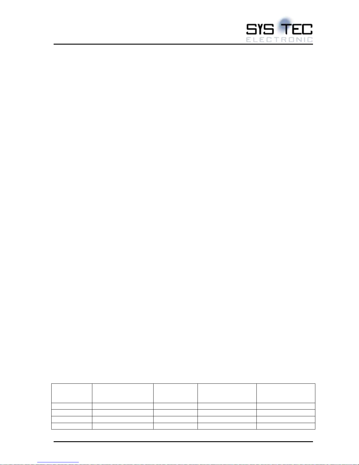
an I2C device has an input capacitance of 8pF. A PCB trace has 0.15pF/mm of trace length. The Table
10 shows the recommendations.
LS1021A
signal name
ECUcore I2C-
interface line name
Module pull-
up
Minimum pull-up
resistor on Carrier
board
Maximum
capacitance on
Carrier board
IIC1_SCL
I2C1_SCL
7.5kΩ
>1.2kΩ
<85pF
IIC1_SDA
I2C1_SDA
7.5kΩ
>1.2kΩ
<85pF
IIC2_SCL
SDHC_/CD/I2C2_SCL
-
>1kΩ
<100pF
IIC2_SDA
SDHC_WP/I2C2_SDA
-
>1kΩ
<100pF
Page 26
SYS TEC electronic GmbH
L-1589e-04 Hardware Manual ECUcore-1021
Page 26/30
Classification: Release
IIC3_SCL
SPI1_SCK
-
>1kΩ
<100pF
IIC3_SDA
QSPI_DIO_B3
-
>1kΩ
<100pF
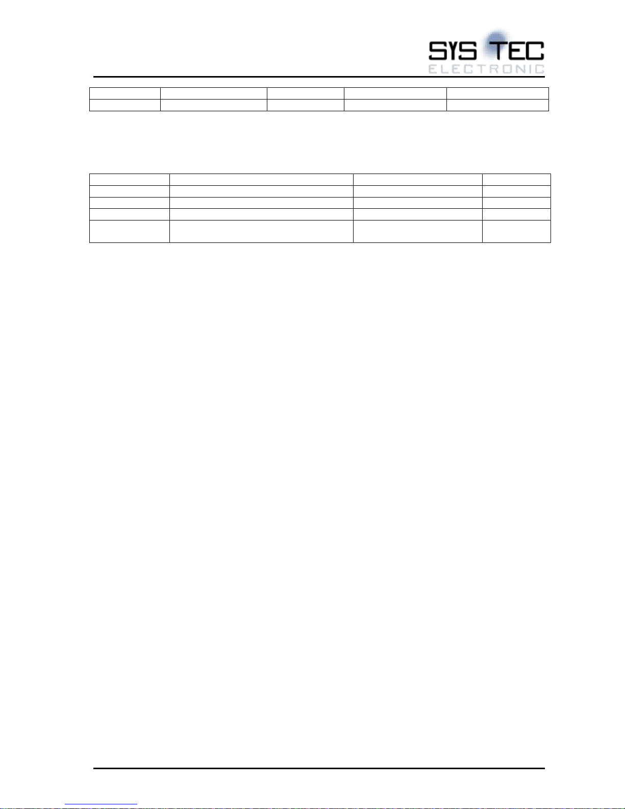
Table 10: I2C line pull-up resistors
Each I2C device has a device address. The Table 11 shows the on-board existing devices (depends on
ordered module configuration), the addresses and the maximum bit rate.
I2C device
Description
I2C 7-bit device address
Bit rate
ADM1032
Temperature sensor
0x4C
400kHz
PC34VR500V1
PMIC
0x08
400kHz
RTC8564
Real time clock
0x51
400kHz
Reserved
Do not use this device address on
Carrier Board.
0x69
-
Table 11: I2C device addresses and bit rates
3.11 Temperature sensor
An on-board temperature sensor measures the CPU internal temperature. The measured temperature is
compared with the corresponding programmed temperature limits. Exceeding the temperature limits
causes the THERM_/CRIT output to assert low (see module pin connector). The temperature limits can
be programmed via I2C interface (see chap. 3.10 for I2C device addressing).
3.12 System Diagnostics Controller (SDC, optional)
The SDC provides the following properties:
- Independently Window-Watchdog timer
- Real Time Clock (RTC)
- Analog voltage input
The SDC is supplied with power by the VBAT pin and 3V3_D1VDD power supply domain.
3.12.1 Window-Watchdog timer
The Module provides a window-watchdog timer which is independently form the CPU clock. The
watchdog is a part of the on-board System Diagnostics Controllers (SDC). The watchdog can generate a
signal (SDC_WDTO) to reset the system and Carrier Board if the system hangs for a long time. The
signal SDC_WDTO is high-active.
The watchdog starts with the first detected pulse at the input SDC_WDTI or if a Watchdog Trigger
command was received by the SDC. The default watchdog timeout (upper threshold) is 60s and can be
configured to lower values (value range: 100ms … 60000ms). The default lower threshold of watchdog
timeout is 0ms and can be configured to higher values (value range: 10ms … 1000ms).
3.12.2 Real Time Clock (RTC)
The RTC is supplied by power supply domain 3V3_D1VDD and by a battery connected to pin VBAT. The
RTC keeps the time if the 3V3_D1VDD is switched off. For this operating state the RTC change-over to a
very low current operating mode.
3.13 Deep sleep mode considerations
DSM (Deep Sleep Mode) is not supported in the latest version. The module connector pin assignment is
prepared to support this feature in a future version. Ask sales department for supporting DSM feature.
If no DSM is used, then the pins and 3V3_D1VDD und 3V3 must be powered from the same power
supply on Carrier Board.
Page 27
SYS TEC electronic GmbH
L-1589e-04 Hardware Manual ECUcore-1021
Page 27/30
Classification: Release
3.14 Thermal Design considerations
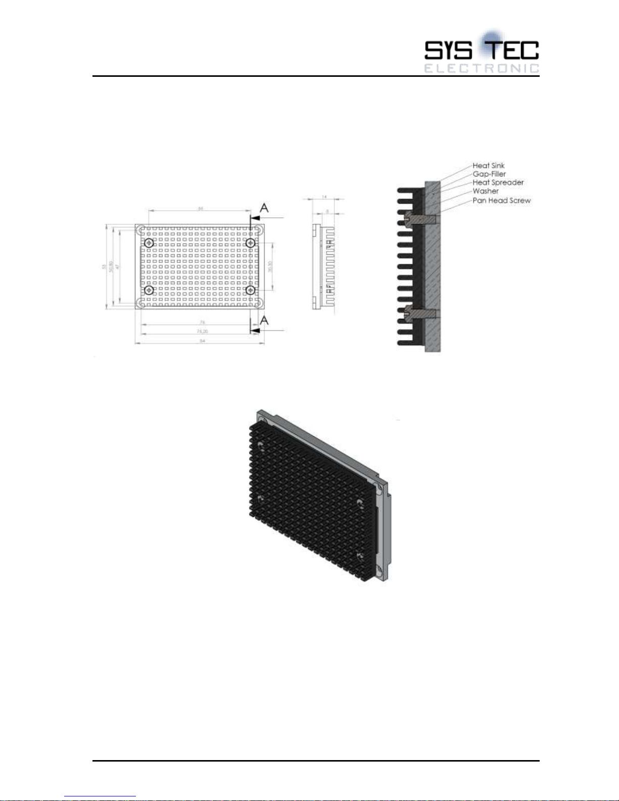
An example for using a heat sink mounted on heat spreader shows Figure 5.
Figure 5: Heat spreader with mounted heat sink (dimension and details)
Figure 6: Heat spreader with mounted heat sink (example)
Page 28
SYS TEC electronic GmbH
L-1589e-04 Hardware Manual ECUcore-1021
Page 28/30
Classification: Release
4 Application Carrier Board (optional)
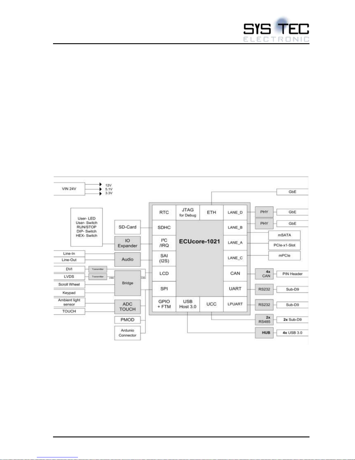
The carrier board delivered with the Application Kit ECUcore-1021 integrates a broad number of
commonly used high-speed interfaces like Gigabit Ethernet, USB3.0, SATA3.0, PCI-Express, LVDS, DVI
and SD-Card. In addition various other communication interfaces and user-input elements are available
on the board, including CAN, RS485, RS232, PMOD, Arduino, keypad, scroll-wheel, audio, push buttons
and LEDs. The delivered schematic diagram of the Application Carrier Board may serve as a base for
own hardware designs and accelerates the development time significantly by eliminating typical pitfalls
when it comes to the LS1021A chip configuration or power-supply design.
This vast variety of on-board peripherals is an ideal base for implementation of own IoT gateway
applications. Supported by an industry-proven Linux version and up to 3 Gigabit Ethernet ports the
Application Carrier Board integrates well in existing IT infrastructures. In addition it supports WLAN
interface cards connected via MiniPCIe socked.
The on-board SD-Card as well as the mSATA socked allow for easy integration of mass-storage devices
onto the Application Carrier Board.
Figure 7: Block diagram ECUcore-1021 with Application Carrier Board
For use in applications where user interaction is required, the Application Carrier Board offers an interface
to connect LVDS capable LCD screens or a DVI socket for use with standard COTS monitor devices. A
dedicated touch screen controller is available for connecting resistive touch screens and accessing the
on-board ambient light sensor. A dedicated 4x4 keyboard matrix input on a standard 2.54mm pitch pinheader connector allows for interfacing user-specific keypads. Alternatively, you can also use common
Human Interface Devices (HID) like keyboard or mouse connected via USB. In case you wish to use the
ECUcore-1021 in networked HMI device applications, the on-board scroll wheel with click-input function is
an ideal choice for an simplified input device for target visualizations where the use of a keypad or USB
connected input devices are not favorable.
Page 29

SYS TEC electronic GmbH
L-1589e-04 Hardware Manual ECUcore-1021
Page 29/30
Classification: Release
A single frequency beeper device is available for acoustic signaling. In addition, the Application Carrier
Board offers a dedicated audio channel with stereo line-in/line-out.
To support an easy and standardized local I/O extension the Application Carrier Board offers one socket
connector for interfacing Arduino Shields and two PMOD sockets, the standard interface to connect
sensors from Analog Devices. A number of push-buttons, switches and LEDs, as well as a temperature
sensor are already integrated on-board.
Users with higher demands in I/O functionality may extend functions using the on-board PCI-Express slot
e.g. for connecting FPGA cards or use the available USB3.0 ports. At the same time common field bus
interfaces like Ethernet, CAN or RS485 are available for remote I/O extension. Please contact us for
supported field bus protocols such as POWERLINK, CANopen and/or Modbus.
The Application Kit includes an Application Carrier Board with pre-assembled ECUcore-1021 and heatspreader plate. The DVD contains the development environment for C/C++ application development on
the ECUcore-1021 pre-installed on a ready-to-use virtual machine (VMware). The delivered
documentation include the Application Carrier Board schematic diagram and its Bill of Material (BOM), the
components used have been selected for applications in industrial environments. The schematic diagram
provides a start point for the development of own application specific boards. The user gets to know the
software environment, can execute performance tests and can begin to write application software.
You are looking for a ready device solution? Please have a look at our IoT Gateway device, where we
offer a special version of our Application Carrier Board with ECUcore-1021 in a professional enclosure
solution with various add-on options.
Page 30
SYS TEC electronic GmbH
L-1589e-04 Hardware Manual ECUcore-1021
Page 30/30
Classification: Release
5 Release and Comments
Released by
Date,Signature
Comments regarding the release:
 Loading...