

Page 1
SUPPLEMENT
SERVICE MANUAL
This service manual shows only the differences between
the model WF15L5 and the original model 6615LF4.
All other information is described in the service manual
of the model 6615LF4.
15″ COLOR LCD
TELEVISION
WF15L5
TABLE OF CONTENTS
Block Diagrams . . . . . . . . . . . . . . . . . . . . . . . . . . . . . . . . . . . . . . . . . . . . . . . . . . . . . 1-1
Schematic Diagrams / CBA's and Test Points . . . . . . . . . . . . . . . . . . . . . . . . . . . . . . 2-1
Waveforms. . . . . . . . . . . . . . . . . . . . . . . . . . . . . . . . . . . . . . . . . . . . . . . . . . . . . . . . . 3-1
Wiring Diagram . . . . . . . . . . . . . . . . . . . . . . . . . . . . . . . . . . . . . . . . . . . . . . . . . . . . . 4-1
Different parts from the original model (6615LF4). . . . . . . . . . . . . . . . . . . . . . . . . . . 5-1
Page 2
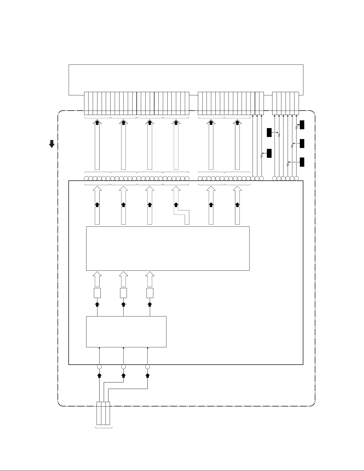
BLOCK DIAGRAMS
System Control Block Diagram
SENSOR
KEY SWITCH
CLN104
CN104
REMOTE
KEY SWITCH
RCV101
KEY-IN-122
KEY-IN-211
REMOTE66
CN113 IS USED
FOR ADJUSTMENT
AT FACTORY
TO POWER SUPPLY
BLOCK DIAGRAM
BLOCK DIAGRAM
P-ON-H
P-ON-H2
FUNCTION CBA
TO LCD BACKLIGHT
BACKLIGHT-SW
BACKLIGHT-ADJ
TO IF/VIDEO
BLOCK DIAGRAM
FSC
SCL
SDA
S-SW
INPUT-0
AFT-IN
INPUT-1
P-ON-H
VOLUME
TO AUDIO
BLOCK DIAGRAM
SDA
SCL
AUDIO-MUTE
SDA2SCL1BUS-OPEN
4
CN113 (NO CONNECTION)
IC333 (TV MICRO CONTROLLER)
4KEY-IN-2
3
KEY-IN-1
MAIN CBALCD MAIN CBA UNIT
FSC123
BACKLIGHT-SW
BACKLIGHT-ADJ
P-ON-H16 8
INPUT-012 12
INPUT-111 13
P-ON-H214 10
19 5
21 3
CN102B CN102A
TO POWER
SUPPLY
BLOCK
P-25V-ON
12
P-25V-ON
DIAGRAM
221817
23
BUS-OPEN
BACKLIGHT-SW
BACKLIGHT-ADJ
16
P-ON-H
P-ON-H2
3140193241
INPUT-0
INPUT-1
P-ON+3.3V(D)
X161
27MHz
RESET
Q151
11
REMOTE
21
RESET
42
XIN
43
XOUT
S-SW717
SCL618
SDA519
AFT-IN10 14
5AFT-IN
SCL
SDA
S-SW
VOLUME15 9
AUDIO-MUTE
13 11
20
35
VOLUME
AUDIO-MUTE
Q301
Q131
80
TUNERCLK
IC171
(MEMORY)
BUFFER
3.3V<-->5V
CONVERTER
7
6
5
WP
SCL
SDA
BUS-OPEN519
CN103B CN103A
CN112(NO CONNECTION)
SDA 2
SCL 1
BUS-OPEN 4
NO PART
MOUNTED
FOR CN112
1-1
L3120BLS
Page 3
IF/Video Block Diagram
TO
LCD BLOCK
DIAGRAM
CVBS11
S-VIDEO-C7
CN103B
S-VIDEO-Y9
AUDIO SIGNAL
MAIN CBA
VIDEO SIGNAL
TO AUDIO BLOCK
DIAGRAM
SIF
8
SIF
AMP
7
4.5MHz
FILTER
CF31
SIF
TRAP
BUFFER
4
5
WF9
WF8
Q702
13
BUFFER
14
12
Q701
1
BUFFER
15
2
SW
TO AUDIO
BLOCK DIAGRAM
INPUT-0(INV)
INPUT-1(INV)
11
10
CONTROL
9
Q707
Q708
INPUT-0
INPUT-1
CN103A
WF7
TO SYSTEM CONTROL
BLOCK DIAGRAM
AFT-IN
13
18
EQ
AMP
1
Q703
IC781 (INPUT SELECT)
3
BUFFER
Q32
4
VIDEO
VIF
IC31 (IF SIGNAL PROCESS)
16
SAW
FILTER
SF11
IF
TU1
(TUNER UNIT)
DET
AMP
17
VCO
IF AGC DET
RF
AGC
14
5
173
AGC
XTAL-IN
2
SCL
AFT
2
DEFEAT
AMP
11
SDA
SDA
TO
FSC
SCL
SYSTEM
CONTROL
BLOCK
S-SW
DIAGRAM
JK703
VIDEO1
CY
-IN
JK701
S-VIDEO
IN
TO SYSTEM CONTROL
BLOCK DIAGRAM
1- 2 L3120BLIF
Page 4
Audio Block Diagram
AUDIO SIGNAL
30
L-CH
OFFSET
CANCEL
75uS
DE-EMPH
MATRIX AGC
29
R-CH
OFFSET
CANCEL
WIDE BAND
EXPAND
WIDE BAND
RMS DET
WIDE BAND
FILTER
(L-R)/SAP
SW
SPECTRAL
EXPAND
dBX
DE-EMPH
SPECTRAL
RMS DET
SPECTRAL
FILTER
SP802
SPEAKER
L-CH
CLN802
SP-L 1
CN802
SP801
SPEAKER
R-CH
JK801
HEADPHONE
JACK
GND 2
WF6
VOLUME
/STANDBY
CONTROL
14
RF
AMP
11
AMP
MUTE
CLN801
GND 2
SP-R 1
CN801
TO IF/VIDEO
SCL
BLOCK DIAGRAM
SDA
INPUT-0(INV)
INPUT-1(INV)
TO SYSTEM
CONTROL BLOCK
VOLUME
P-ON-H
AUDIO-MUTE
Q803
5
7
2
Q802
+5V
IC851 (MTS/SAP AUDIO SIGNAL PROCESS)
L+R
FILTER
OFFSET
STEREO
FILTER
SIF/BB
SW
INPUT
VCA
SIF
DEMOD
21
SIF
L-R
FILTER
CANCEL
SAP OUT
FILTER
SAP
DEMOD
SAP
FILTER
I2C
DECORDER
27
24
IC801 (AUDIO AMP)
13
TUNER
AUDIO1
IC852 (INPUT SELECT)
111512
14
14
(L-CH)
6
(L-CH)
(R-CH)
TUNER
4
(R-CH)
1
3
AUDIO1
2
9 10
SW CTL
1
5
MAIN CBA
TO
IF/VIDEO BLOCK
DIAGRAM
1-3
AUDIO1(L)
JK704
-IN
JK705
AUDIO1(R)
-IN
L3120BLA
Page 5
LCD Block Diagram
LCD MODULE
OR(0)34
OR(2)32
OR(3)31
OR(1)33
OR(4)30
OR(5)29
OG(0)27
OG(1)26
OG(2)25
OG(3)24
OG(4)23
OG(5)22
OB(0)20
OB(1)19
OB(2)18
OB(3)17
OB(4)16
OB(5)15
ER(0)6
ER(1)5
ER(2)4
ER(3)3
ER(4)2
ER(5)1
EG(0)50
EG(1)49
EG(2)48
EG(3)47
EG(4)46
EG(5)45
EB(0)43
EB(1)42
EB(2)41
EB(3)40
EB(4)39
EB(5)38
OFFEV12
STV113
CLKV14
HMS1-E7
HMS1-013
STH142
POL43
LP44
CLKH10
VIDEO SIGNAL
LCD MAIN CBA UNIT
CN311
170
169
166
R(ODD)
R
165
164
163
162
161
157
156
G(ODD)
G
155
154
153
152
148
B(ODD)
B
147
146
145
LCD RGB
138
137
SIGNAL
PROCESS
136
135
130
129
R(EVEN)
CN312
128
127
126
125
G(EVEN)
118
117
116
115
114
113
B(EVEN)
108
107
101
105
STV1
OFFEV
R365
106
CLKV
CN311
WF1
WF2
R392
144
143
CLKH1
ODDINV
R202
R394
139
172
173
POL
STH-1
EVENINV
WF4
R201
WF3
WF5
174
LP
IC333 (LCD DRIVE / SIGNAL PROCESS)
A/D
R
CVBS
68
CN103B
CVBS 13
TO
IF/VIDEO
S-VIDEO-Y 15
S-VIDEO-C 17
BLOCK
DIAGRAM
CN103A
A/D
G
VIDEO
SIGNAL
C
49
PROCESS
A/D
B
Y
71
1-4
L3120BLLCD
Page 6
SCHEMATIC DIAGRAMS / CBA'S AND TEST POINTS
Standard Notes
Many electrical and mechanical parts in this chassis have special characteristics. These characteristics often
pass unnoticed and the protection afforded by them cannot necessarily be obtained by using replacement
components rated for higher voltage, wattage, etc. Replacement parts that have these special safety
characteristics are identified in this manual and its supplements; electrical components having such features are
identified by the mark “#” in the schematic diagram and the parts list. Before replacing any of these components,
read the parts list in this manual carefully. The use of substitute replacement parts that do not have the same
safety characteristics as specified in the parts list may create shock, fire, or other hazards.
Notes:
1. Do not use the part number shown on these drawings for ordering. The correct part number is shown in the
parts list, and may be slightly different or amended since these drawings were prepared.
2. All resistance values are indicated in ohms (K = 10
3. Resistor wattages are 1/4W or 1/6W unless otherwise specified.
4. All capacitance values are indicated in µF (P = 10
5. All voltages are DC voltages unless otherwise specified.
Note of Capacitors:
ML --- Mylar Cap. PP --- Metallized Film Cap. SC --- Semiconductor Cap. L --- Low Leakage type
Temperature Characteristics of Capacitors are noted with the following:
B --- ±10% CH --- 0±60 ppm/°C CSL --- +350~-1000 ppm/°C
3
, M = 106).
-6
µF).
Tolerance of Capacitors are noted with the following:
Z --- +80~-20%
Note of Resistors:
CEM --- Cement Res. MTL --- Metal Res. F --- Fuse Res.
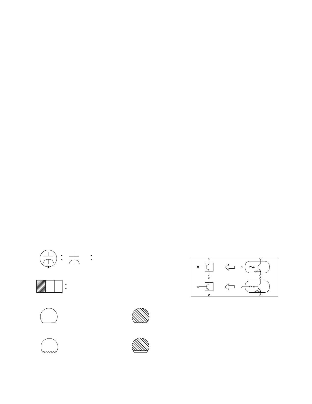
Capacitors and transistors are represented by the following symbols.
CBA Symbols
(Top View) (Bottom View)
+
Electrolytic Capacitor
(Bottom View)
Transistor or Digital Transistor
E C B
(Top View)
NPN Transistor
E C B
(Top View)
(Top View)
PNP Transistor
E C B
(Top View)
Schematic Diagram Symbols
Digital Transistor
E C B
NPN Digital Transistor
PNP Digital Transistor
E C B
2-1 LC2N_SC
Page 7

LIST OF CAUTION, NOTES, AND SYMBOLS USED IN THE SCHEMATIC DIAGRAMS ON
THE FOLLOWING PAGES:
1. CAUTION:
CAUTION: FOR CONTINUED PROTECTION AGAINST RISK OF FIRE, REPLACE ONLY WITH SAME
TYPE_A,_V FUSE.
ATTENTION: UTILISER UN FUSIBLE DE RECHANGE DE MÊME TYPE DE_A,_V.
2. CAUTION:
Fixed Voltage (or Auto voltage selectable) power supply circuit is used in this unit.
If Main Fuse (F601) is blown, first check to see that all components in the power supply circuit are not
defective before you connect the AC plug to the AC power supply. Otherwise it may cause some components
in the power supply circuit to fail.
3. Note:
1. Do not use the part number shown on the drawings for ordering. The correct part number is shown in the
parts list, and may be slightly different or amended since the drawings were prepared.
2. To maintain original function and reliability of repaired units, use only original replacement parts which are
listed with their part numbers in the parts list section of the service manual.
4. Voltage indications on the schematics are as shown below:
Plug the TV power cord into a standard AC outlet.:
2
(Unit: Volt)
1
5.0
(3.0)
3
5.0
(3.0)
Power on mode
Power off mode
5. How to read converged lines
1-D3
Distinction Area
Line Number
(1 to 3 digits)
Examples:
1. "1-D3" means that line number "1" goes to the line number
"1" of the area "D3".
2. "1-B1" means that line number "1" goes to the line number
"1" of the area "B1".
6. Test Point Information
: Indicates a test point with a jumper wire across a hole in the PCB.
: Used to indicate a test point with a component lead on foil side.
: Used to indicate a test point with no test pin.
: Used to indicate a test point with a test pin.
Voltage
Indicates that the voltage
is not consistent here.
3
2
1
AREA D3
1-B1
AREA B1
1-D3
ABCD
2-2 LC2N_SC
Page 8

Main 1/5 Schematic Diagram
MAIN 1/5
Ref No. Pos it ion
IC531
D-4
IC533
E-3
IC671
E-2
IC672
E-2
Q501 C-4
Q502 C-4
Q503 B-3
Q505 C-3
Q509 C-3
Q510 B-2
Q511 C-3
Q512 C-2
Q513 C-2
Q531 D-3
Q633 E-1
CN101A A-4
CN102A A-3
ICS
TRANSISTORS
CONNECTORS
2-3
L3120SCM1
Page 9

Main 2/5 Schematic Diagram
MAIN 2/5
Ref No. Pos it ion
IC31 I-1
IC851 H-3
IC852 J-4
Q32 J-2
CN113 G-1
ICS
TRANSISTOR
CONNECTOR
2-4
L3120SCM2
Page 10

Main 3/5 Schematic Diagram
MAIN 3/5
Ref No. Pos it ion
IC781
P-3
IC801
N-2
Q701
N-3
Q702
N-3
Q703 N-3
Q704 P-1
Q705 O-1
Q706 P-1
Q707 P-2
Q708
P-2
Q802
O-1
Q803
N-1
CN801
M-4
CN802 M-3
CN103A M-2
ICS
TRANSISTORS
CONNECTORS
2-5
L3120SCM3
Page 11

Main 4/5 Schematic Diagram
MAIN 4/5
Ref No. Pos it ion
IC601
U-1
Q601 S-2
Q603
T-2
Q661 W-2
TP402 X-4
TRANSISTORS
IC
TESTPOINT
CAUTION !
Fixed voltage (or Auto voltage selectable) power supply circuit is used in this unit.
If Main Fuse (F601) is blown , check to see that all components in the power supply
circuit are not defective before you connect the AC plug to the AC power supply.
Otherwise it may cause some components in the power supply circuit to fail.
4A/125V
CAUTION ! :
ATTENTION : Utiliser un fusible de rechange de même type de 4A, 125V.
For continued protection against risk of fire,
replace only with same type 4 A, 125V fuse.
NOTE:
The voltage for parts in hot circuit is measured using
hot GND as a common terminal.
2-6
L3120SCM4
Page 12

Main 5/5 Schematic Diagram
MAIN5/5
Ref No. Pos it ion
Q401 AA-2
Q403 Z-2
Q404 Z-3
Q405 AA-2
Q406 AA-2
Q407 Z-3
Q408 Z-4
Q409 Z-2
Q410 Z-3
Q411 AA-3
Q412 AA-3
Q415 AA-1
Q416 AA-1
Q421 AC-4
Q422 AC-3
Q423 AC-2
Q424 AB-1
Q427 AA-3
Q428 AA-2
CN402
AD-4
CN403
AD-2
TP403 Z-3
TRANSISTORS
CONNECTORS
TESTPOINT
2-7
L3120SCM5
Page 13

Function Schematic Diagram
2-8
L3120SCF
Page 14

LCD Main 1/2 Schematic Diagram
LCD MAIN 1/ 2
Ref No. Pos it ion
IC333
B-3
Q301
D-1
CN104
A-3
CN105
A-2
CN111
A-2
CN211
F-4
CN311 F-4
CN102B A-4
CONNECTORS
IC
TRANSISTOR
2-9
L3120SCL1
Page 15

LCD Main 2/2 Schematic Diagram
LCD MAIN 2/ 2
Ref No. Pos it ion
IC151 I-3
IC171
J-3
IC191
H-2
IC192
H-1
IC193
H-2
IC201 J-1
Q131
I-4
Q201 J -1
CN112
L-4
CN312
L-3
CN101B
L-4
CN103B G-2
ICS
CONNECTORS
TRANSISTORS
2-10
L3120SCL2
Page 16

WAVEFORMS
WF1 ~ WF9 = Waveforms to be observed at
Waveform check points.
(Shown in Schematic Diagram.)
Input: NTSC Color Bar Signal (with 1kHz Audio Signal)
CLKH
WF1
CLKV
WF2
1DIV: 1.0V 10 s
R392
1DIV: 1.0V 20ns
R365
LP
WF4
STH1
WF5
1DIV: 1.0V 10
R201
1DIV: 1.0V 10
R394
CVBS
s
WF7
1DIV: 200mV 20
s
Pin 11 of CN103A
S-VIDEO-Y
s
WF8
1DIV: 200mV 20
s
Pin 9 of CN103A
POL
WF3
1DIV: 1.0V 20
R202
AUDIO
s
WF6
1DIV: 100mV 400
s
Pin 14 of IC801
S-VIDEO-C
WF9
1DIV: 200mV 20 s
Pin 7 of CN103A
L3120WF3-1
Page 17

WIRING DIAGRAM
NU
PANEL+10.8V
GND
NU
PANEL+3.3V
CN101B
9
7
6
8
215
3
4
NU
NU
GND
CN101A
PANEL+3.3V
PANEL+10.8V
BACKLIGHT-ADJNUGND
GND
CN102A
CN102B
BACKLIGHT-SWNUNU
132547689
19
232120
22
NU
GND
GND
BACKLIGHT-SW
BACKLIGHT-ADJ
LCD MAIN CBA
CN103B
GND
PANEL+25V
PANEL-6V
GND
4
7
6
GND
PANEL+25V
18
17
NU
NU
CN801
SP-R
1
2
8
PANEL-6V
P-ON-H
161113
P-ON-H
GND
2
CLN801
NU
GND
NU
153
232120
22
9
153
2
NU
NU
GND
GND
CN103A
AUDIO-MUTE
VOLUME
P-ON-H2
INPUT-0
INPUT-1
10131211141517161918212022
14
12
15
INPUT-0
INPUT-1
P-ON-H2
VOLUME
AUDIO-MUTE
GND
NU
19
4
NU
GND
PROTECT-1
AFT-IN
9
10
AFT-IN
PROTECT-1
CN802
SP-L
1
S-VIDEO-C
GND
18
17
7
6
GND
S-VIDEO-C
PROTECT-2
S-SW
724
8
S-SW
PROTECT-2
GND
2
CLN802
GND
GND
S-VIDEO-Y
14
161113
15
9
8
101412
GND
GND
S-VIDEO-Y
SDA
SCL
GND
6
SCL
SDA
GND
CVBS
GNDNUGNDNUAL+3.3V(A)
9
10
12
11
13
15
NU
GNDNUGND
CVBS
AL+3.3V(A)
P-25V-ON
GND
AL+5V
23
153
GND
AL+5V
P-25V-ON
AC CORD
AC601
NU
DVD-MAIN-POWER(NU)
724
6
8
18
16
17
NU
DVD-MAIN-POWER(NU)
(NO CONNECTION)
CN113
GND
AL+7V(D)
BUS-OPEN
1923212022
GND
AL+7V(D)
BUS-OPEN
GND
SCL
SDA
134
2
GND
FSC
153
FSC
GND
CN113 IS USED
FOR ADJUSTMENT
BUS-OPEN
MAIN CBA
AT FACTORY
KEY-IN-2
AL+3.3V
KEY-IN-1
CN104
132
1
3
2
CLN104
AL+3.3V
KEY-IN-2
KEY-IN-1
TU1 TUNER UNIT
GND
4
4
GND
NUNUREMOTE
576
576
NU
NU
8
8
NU
NU
REMOTE
FUNCTION CBA
AUDIO1
(L)-IN
AUDIO1
(R)-IN
VIDEO1
-IN
S-VIDEO
OUT IN
1
CN312
GND
2NU3
CN311
5NU6
V-COM4V-COM
SP801
SPEAKER
GND
HMS1-E
ER(0)
ER(1)
ER(2)
ER(3)
ER(4)
ER(5)
132547689
7NU8
9
10
11NU12
13
NU
VDDG(+25V)
VDDD(+3.3V)
OFFEV
VEEG(-6V)
STV1
SP802
SPEAKER
GND
CLKH
GND
GND
HMS1-0
GND
OB(5)
OB(4)
OB(3)
OB(2)
OB(1)
OB(0)
GND
OG(5)
OG(4)
OG(3)
OG(2)
OG(1)
OG(0)
101312111415171619182120222324272625282930
14
15
16
CLKV
XAO
GND
17NU18NU19NU20NU21
22
GND
VREF(9)23VREF(8)24VREF(7)25VREF(6)26VREF(5)
27
28
GND
VREF(4)29VREF(3)30VREF(2)31VREF(1)32VREF(0)
GND
OR(5)
OR(4)
OR(3)
33
35
V-COM36V-COM
VDDA(+10.8V)34VDDA(+10.8V)
CN402
2
1
BACK
LIGHT
OR(2)
OR(1)
OR(0)
GND
GND
VDDD(+3.3V)
33
32313435373639384140424344
37
38
GND
EB(5)39EB(4)40EB(3)41EB(2)42EB(1)43EB(0)
CN403
VDDD(+3.3V)
VDDD(+3.3V)
VDDD(+3.3V)
GND
44
45
GND
EG(5)46EG(4)47EG(3)48EG(2)49EG(1)50EG(0)
2
1
BACK
LIGHT
STH1
POLLPGND
45
LCD MODULE
L3120WI4-1
Page 18

Different parts from the original model (6615LF4)
Ref. No. Description Part No.
MECHANICAL PARTS
A1 FRONT CABINET L0200UA 1EM020010C
A2 Not used
A3 CONTROL PLATE L3120UL 1EM320480
A4 REAR CABINET L3120UL 1EM120388
# RATING LABEL L3120UL ----------
A6
B4 JACK HOLDER L3120UL 1EM320461
S1 CARTON L3120UL 1EM421264
S2 STYROFOAM TOP L3100UA 1EM020146A
S3 STYROFOAM BOTTOM L3100UA 1EM020147A
S6 LABEL EAS(H3761UD) MAKER
X2
X3 REMOCON UNIT 170/ECNLC301/
ELECTRICAL PARTS
C158 Not used
C162 CHIP CERAMIC CAP. CH J 11pF/
C177 CHIP CERAMIC CAP.(1608) CH J
C178 CHIP CERAMIC CAP.(1608) CH J
C190 CHIP ELECTROLYTIC CAP. 47µF/
C331 Not used
C722 Not used
C726 Not used
C730 Not used
C734 Not used
C735 Not used
C736 Not used
C751 Not used
C752 Not used
C753 Not used
C754 Not used
D191 ZENER DIODE EDZTE61 4.7B QD1B00EDZ4R7
D701 Not used
D702 Not used
D703 Not used
IC191 VOLTAGE REGULATOR
IC192 VOLTAGE REGULATOR
IC333 DIGITAL VIDEO PROCESSOR
JK706 Not used
JK707 Not used
JK708 Not used
JK709 Not used
JK710 Not used
Q704 Not used
NO.ZLLFNSLE1
# OWNERS MANUAL L3120UL 1EMN20510A
NE903UD
LCD MAIN CBA & LIQUID
CRYSTAL PANEL UNIT
MMA CBA 1ESA11081
MAIN CBA ----------
50V
68pF/50V
68pF/50V
10V
PQ1LAX95MSPQ
LD1117SC-R
R8A01014A92FP
----------
NE903UD
1FSA10070
CHD1JJ3CH110
CHD1JJ3CH680
CHD1JJ3CH680
CA1A470SP062
QSZBA0TSH053
NSZBA0TSS229
QSZAA0RHT070
Ref. No. Description Part No.
Q705 Not used
Q706 Not used
R140 Not used
R143 Not used
R145 Not used
R164 Not used
R165 Not used
R167 Not used
R189 CHIP RES.(1608) 1/10W J 10k Ω RRXAJR5Z0103
R190 CHIP RES.(1608) 1/10W J 100 Ω RRXAJR5Z0101
R192 CHIP RES.(1608) 1/10W F 240 Ω RRXAFR5H2400
R193 CHIP RES. 1/10W F 1.2k Ω RRXAFR5H1201
R195 CHIP RES.(1608) 1/10W J 1k Ω RRXAJR5Z0102
R196 CHIP RES. 1/10W F 3.0k Ω RRXAFR5Z3001
R197 CHIP RES. 1/10W F 1.8k Ω RRXAFR5Z1801
R732 Not used
R733 Not used
R734 Not used
R735 Not used
R736 Not used
R738 Not used
R739 Not used
R740 Not used
R741 Not used
R742 Not used
R743 Not used
R744 Not used
R747 Not used
R748 Not used
R749 Not used
R752 Not used
R755 Not used
R756 Not used
R757 Not used
R758 Not used
R759 Not used
R820 Not used
R821 Not used
R826 Not used
R827 Not used
R831 Not used
R832 Not used
R833 Not used
R834 Not used
5-1 L3120PL
Page 19

WF15L5
L3120UL
2005-06-25
 Loading...