

Page 1
SERVICE MANUAL
Sec. 1: Main Section
I Specifications
I Preparation for Servicing
I Adjustment Procedures
I Schematic Diagrams
I CBA’s
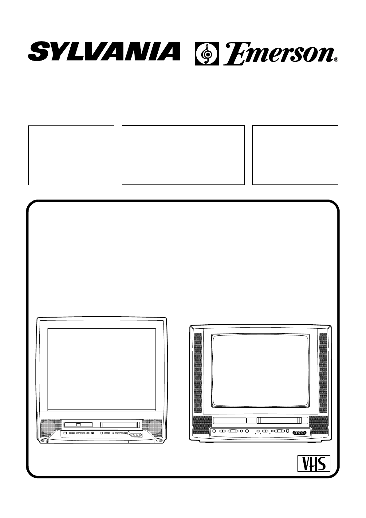
19" COLOR TV/DVD/VCR
6719DC/
SSC719C
Sec. 2: Deck Mechanism Section
I Standard Maintenance
I Alignment for Mechanism
I Disassembly/Assembly of Mechanism
EWC19T2
Sec. 3: Exploded views
and Parts List Section
I Exploded views
I Parts List
Page 2

IMPORTANT SAFETY NOTICE
Proper service and repair is important to the safe, reliable operation of all
Funai Equipment. The service procedures recommended by Funai and
described in this service manual are effective methods of performing service
operations. Some of these service special tools should be used when and as
recommended.
It is important to note that this service manual contains various CAUTIONS
and NOTICES which should be carefully read in order to minimize the risk of
personal injury to service personnel. The possibility exists that improper service methods may damage the equipment. It also is important to understand
that these CAUTIONS and NOTICES ARE NOT EXHAUSTIVE. Funai could not
possibly know, evaluate and advice the service trade of all conceivable ways
in which service might be done or of the possible hazardous consequences of
each way. Consequently, Funai has not undertaken any such broad evaluation. Accordingly, a servicer who uses a service procedure or tool which is not
recommended by Funai must first use all precautions thoroughly so that neither his safety nor the safe operation of the equipment will be jeopardized by
the service method selected.
Manufactured under license from Dolby Laboratories. "Dolby" and
the double-D symbol are trademarks of Dolby Laboratories.
"DTS" and "DTS Digital Out" are trademarks of Digital Theater Systems Inc.
Page 3

MAIN SECTION
19" COLOR TV/DVD/VCR
6719DC/SSC719C/EWC19T2
Sec. 1: Main Section
I Specifications
I Preparation for Servicing
I Adjustment Procedures
I Schematic Diagrams
I CBA’s
TABLE OF CONTENTS
Specifications . . . . . . . . . . . . . . . . . . . . . . . . . . . . . . . . . . . . . . . . . . . . . . . . . . . . . . . . . . . . . . . . . . . . . . . . . . 1-1-1
Laser Beam Safety Precautions . . . . . . . . . . . . . . . . . . . . . . . . . . . . . . . . . . . . . . . . . . . . . . . . . . . . . . . . . . . 1-2-1
Important Safety Precautions. . . . . . . . . . . . . . . . . . . . . . . . . . . . . . . . . . . . . . . . . . . . . . . . . . . . . . . . . . . . . . 1-3-1
Standard Notes for Servicing . . . . . . . . . . . . . . . . . . . . . . . . . . . . . . . . . . . . . . . . . . . . . . . . . . . . . . . . . . . . . . 1-4-1
Preparation for Servicing . . . . . . . . . . . . . . . . . . . . . . . . . . . . . . . . . . . . . . . . . . . . . . . . . . . . . . . . . . . . . . . . . 1-5-1
Operating Controls and Functions . . . . . . . . . . . . . . . . . . . . . . . . . . . . . . . . . . . . . . . . . . . . . . . . . . . . . . . . . . 1-6-1
Cabinet Disassembly Instructions . . . . . . . . . . . . . . . . . . . . . . . . . . . . . . . . . . . . . . . . . . . . . . . . . . . . . . . . . . 1-7-1
Electrical Adjustment Instructions . . . . . . . . . . . . . . . . . . . . . . . . . . . . . . . . . . . . . . . . . . . . . . . . . . . . . . . . . . 1-8-1
FIRMWARE Renewal Mode . . . . . . . . . . . . . . . . . . . . . . . . . . . . . . . . . . . . . . . . . . . . . . . . . . . . . . . . . . . . . . 1-9-1
Block Diagrams . . . . . . . . . . . . . . . . . . . . . . . . . . . . . . . . . . . . . . . . . . . . . . . . . . . . . . . . . . . . . . . . . . . . . . . 1-10-1
Schematic Diagrams / CBA’s and Test Points . . . . . . . . . . . . . . . . . . . . . . . . . . . . . . . . . . . . . . . . . . . . . . . . 1-11-1
Waveforms . . . . . . . . . . . . . . . . . . . . . . . . . . . . . . . . . . . . . . . . . . . . . . . . . . . . . . . . . . . . . . . . . . . . . . . . . . . 1-12-1
Wiring Diagrams . . . . . . . . . . . . . . . . . . . . . . . . . . . . . . . . . . . . . . . . . . . . . . . . . . . . . . . . . . . . . . . . . . . . . . 1-13-1
System Control Timing Charts . . . . . . . . . . . . . . . . . . . . . . . . . . . . . . . . . . . . . . . . . . . . . . . . . . . . . . . . . . . . 1-14-1
IC Pin Function Descriptions . . . . . . . . . . . . . . . . . . . . . . . . . . . . . . . . . . . . . . . . . . . . . . . . . . . . . . . . . . . . . 1-15-1
Lead Identifications . . . . . . . . . . . . . . . . . . . . . . . . . . . . . . . . . . . . . . . . . . . . . . . . . . . . . . . . . . . . . . . . . . . . 1-16-1
Page 4
SPECIFICATIONS
*ˆMode---------SP mode unless otherwise specified
*Test input terminal
<Except Tuner>-------------Video input (1Vp-p)
Audio input (-10dB)
<Tuner>-----------------------Ant. input (80dBµV) Video: 87.5%
Audio: 25kHz dev (1kHz Sin)
<DEFLECTION>
Description Condition Unit Nominal Limit
1. Over Scan — % 90 —
2. Linearity
3. High Voltage — kV 25 —
Horizontal % — 15
Vertical % — 10
<VIDEO & CHROMA>
Description Condition Unit Nominal Limit
Center m/m — 0.4
1. Misconvergence
2. Tint Control Range — deg ±30 —
3. Contrast Control Range — dB 6 2
4. Brightness (100% White Full Field) Contrast: Max ft-L 35 24
5. Color Temperature — K 9200 —
Corner m/m — 2.5
Side m/m — 1.5
<DVD>
Measurement at TP
Description Condition Unit Nominal Limit
1. Horizontal Resolution (TDV-540 TIT.2 CHP.16) — Line 330 320
2. Video S/N at CN3400 (TDV-540 TIT.2 CHP.6) — dB 60 55
3. S/N Chroma at CN3400 AM — dB 58 53
(TDV-540 TIT.2 CHP.17) PM — dB 58 53
4. Audio Distortion (LPCM 48 kHz, W/LPF)
(PTD 1-NOR TIT.1 CHP.1)
5. Audio freq. response (LPCM 48kHz)
(PTD 1-NOR TIT.1 CHP.5 -- 10)
6. Audio S/N (LPCM 48KHz,W/LPF,A-WTD)
(PTD 1-NOR TIT.1 CHP.1 -- 2)
L
R
L, 20 Hz
R, 20 Hz
L, 20 kHz
R, 20 kHz
L
R
1-1-1 T500SP
%
dB 0 +4/-5
dB 100 85
0.03
0.03
0.07
0.07
Page 5
<VCR>
Description Condition Unit Nominal Limit
1. Horizontal Resolution (R/P, SP) Line 230 200
2. Jitter (Low) (R/P, SP) µS0.1 0.2
3. S/N Chroma AM(SP) (R/P, SP) dB 38 33
PM(SP) (R/P, SP) dB 38 33
4. Wow & Flutter (JIS, UNWTD) (R/P, SP) % 0.25 0.5
<TUNER>
Description Condition Unit Nominal Limit
1. Video S/N (80dBµV, TV4ch) — dB 45 40
2. Audio S/N (W/LPF) — dB 45 40
<NORMAL AUDIO>
All items are measured across 8Ω resistor at speaker output terminal.
Description Condition Unit Nominal Limit
1. Audio Output Power (R/P, SP) W 1.0 0.8
2. Audio S/N (W/LPF) (R/P, SP) dB 40 36
3. Audio distortion (W/LPF,-10dB 1kHz IN) (R/P, SP) % 3.0 5.0
4. Audio Freq. Response (-10dB 1kHz IN) 200 Hz (R/P, SP) dB -2.0 -2.0±5.0
8 kHz (R/P, SP) dB 0 0±6.0
<Hi-Fi AUDIO>
* All items are measured at TP1701 and TP1702.
Description Condition Unit Nominal Limit
1. Output Level (-10dB 1kHz IN) (R/P, SP) dB -8.0 -8±4
2. Audio Distortion (-10dB 1kHz IN) (R/P, SP) % 0.5 1.0
3. Freq. Response (-15dB 1kHz IN) 20 Hz (R/P, SP) dB 0 ±4
20 kHz (R/P, SP) dB 0 ±4
Note: Nominal specifications represent the design specifications. All units should be able to approximate these.
Some will exceed and some may drop slightly below these specifications. Limit specifications represent the absolute worst condition that still might be considered acceptable. In no case should a unit fail to meet limit specifications.
1-1-2 T500SP
Page 6
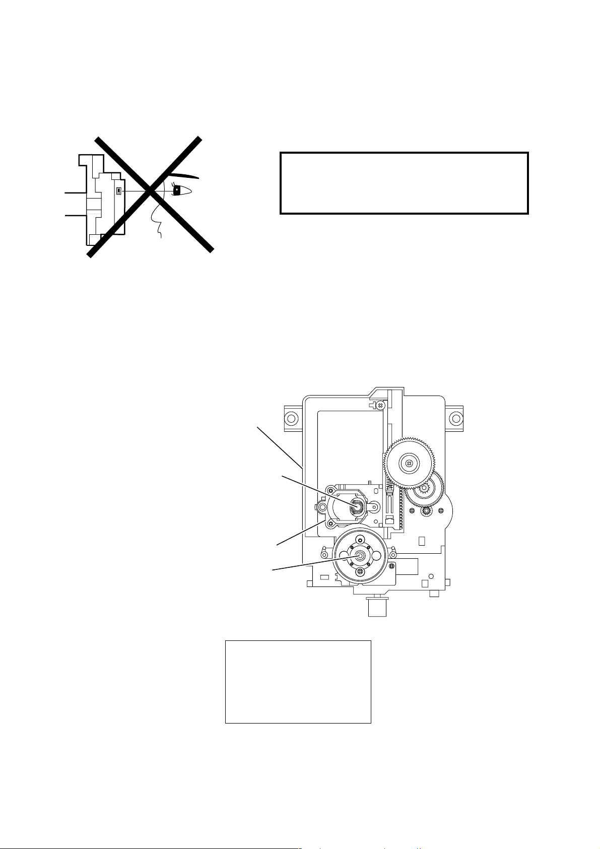
LASER BEAM SAFETY PRECAUTIONS
This DVD player uses a pickup that emits a laser beam.
Do not look directly at the laser beam coming
from the pickup or allow it to strike against
your skin.
The laser beam is emitted from the location shown in the figure. When checking the laser diode, be sure to keep
your eyes at least 30cm away from the pickup lens when the diode is turned on. Do not look directly at the laser
beam.
Caution: Use of controls and adjustments, or doing procedures other than those specified herein, may result in
hazardous radiation exposure.
Drive Mecha Assembly
Laser Beam Radiation
Laser Pickup
Turntable
LASER RADIATION
WHEN OPEN. DO NOT
STARE INTO BEAM.
CAUTION
Location: Inside Top of DVD mechanism.
1-2-1 DVD_LASER
Page 7
IMPORTANT SAFETY PRECAUTIONS
Prior to shipment from the factory, our products are strictly inspected for recognized product safety and electrical
codes of the countries in which they are to be sold. However, in order to maintain such compliance, it is equally
important to implement the following precautions when a set is being serviced.
Safety Precautions for TV Circuit
1. Before returning an instrument to the customer, always make a safety check of the entire instru-
ment, including, but not limited to, the following
items:
a. Be sure that no built-in protective devices are de-
fective and have been defeated during servicing.
(1) Protective shields are provided on this chassis
to protect both the technician and the customer.
Correctly replace all missing protective shields, including any removed for servicing convenience.
(2) When reinstalling the chassis and/or other assembly in the cabinet, be sure to put back in place
all protective devices, including but not limited to,
nonmetallic control knobs, insulating fishpapers,
adjustment and compartment covers/shields, and
isolation resistor/capacitor networks. Do not oper-
ate this instrument or permit it to be operated
without all protective devices correctly installed and functioning. Servicers who defeat
safety features or fail to perform safety checks
may be liable for any resulting damage.
b. Be sure that there are no cabinet openings through
which an adult or child might be able to insert their
fingers and contact a hazardous voltage. Such
openings include, but are not limited to, (1) spacing between the picture tube and the cabinet
mask, (2) excessively wide cabinet ventilation
slots, and (3) an improperly fitted and/or incorrectly
secured cabinet back cover.
c. Antenna Cold Check - With the instrument AC
plug removed from any AC source, connect an
electrical jumper across the two AC plug prongs.
Place the instrument AC switch in the on position.
Connect one lead of an ohmmeter to the AC plug
prongs tied together and touch the other ohmmeter lead in turn to each tuner antenna input exposed terminal screw and, if applicable, to the
coaxial connector. If the measured resistance is
less than 1.0 megohm or greater than 5.2 megohm, an abnormality exists that must be corrected
before the instrument is returned to the customer.
Repeat this test with the instrument AC switch in
the off position.
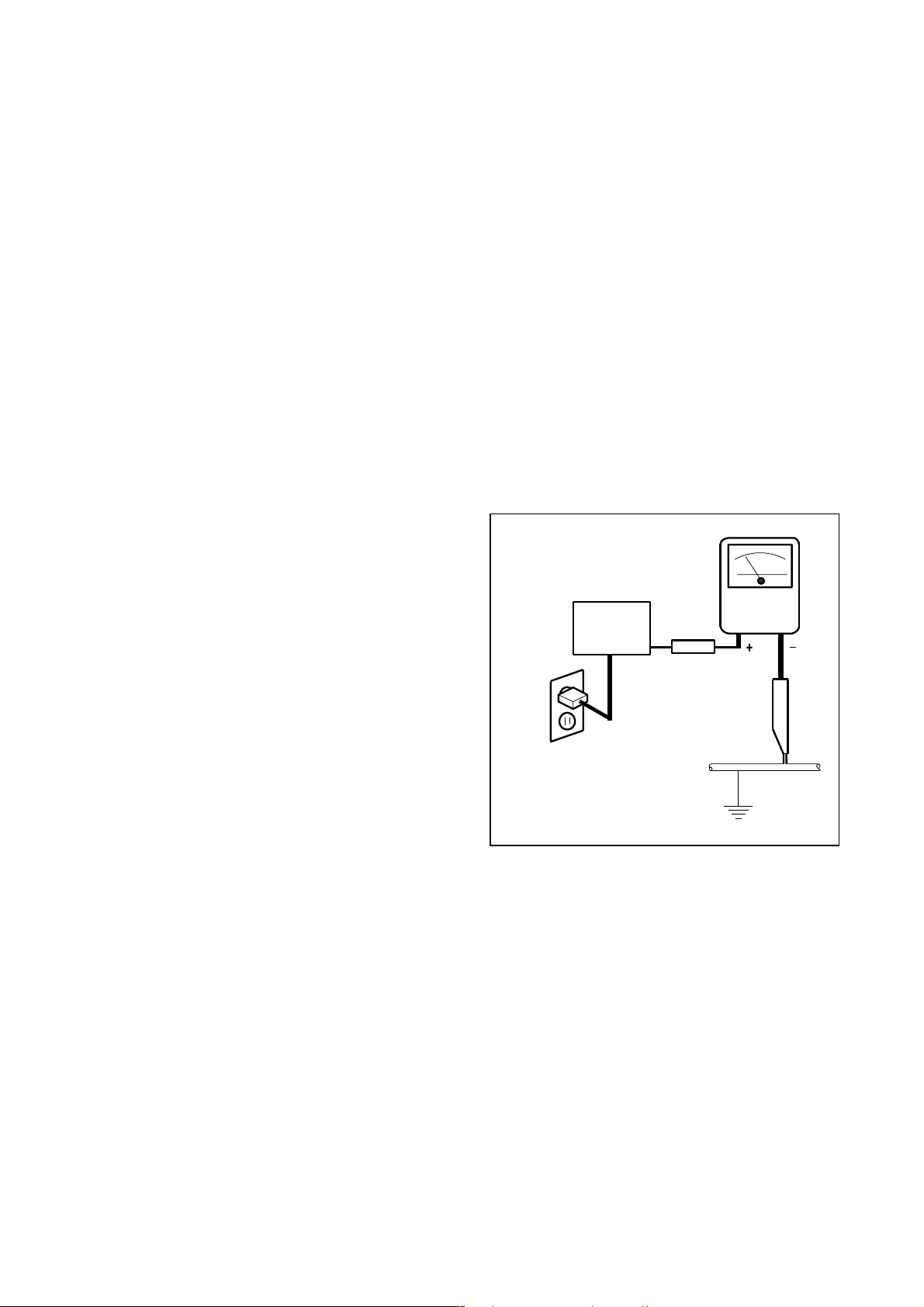
d. Leakage Current Hot Check - With the instru-
ment completely reassembled, plug the AC line
cord directly into a 120V AC outlet. (Do not use an
isolation transformer during this test.) Use a leak-
age current tester or a metering system that complies with American National Standards Institute
(ANSI) C101.1 Leakage Current for Appliances
and Underwriters Laboratories (UL) 1410, (50.7).
With the instrument AC switch first in the on position and then in the off position, measure from a
known earth ground (metal water pipe, conduit,
etc.) to all exposed metal parts of the instrument
(antennas, handle brackets, metal cabinet, screw
heads, metallic overlays, control shafts, etc.), especially any exposed metal parts that offer an electrical return path to the chassis. Any current
measured must not exceed 0.5 milli-ampere. Reverse the instrument power cord plug in the outlet
and repeat the test.
READING SHOULD
NOT BE ABOVE 0.5 mA
LEAKAGE
DEVICE
BEING
TESTED
TEST ALL EXPOSED
METAL SURFACES
ALSO TEST WITH
PLUG REVERSED
USING AC
ADAPTER PLUG
AS REQUIRED
CURRENT
TESTER
EARTH
GROUND
ANY MEASUREMENTS NOT WITHIN THE LIMITS
SPECIFIED HEREIN INDICATE A POTENTIAL
SHOCK HAZARD THAT MUST BE ELIMINATED
BEFORE RETURNING THE INSTRUMENT TO
THE CUSTOMER OR BEFORE CONNECTING
THE ANTENNA OR ACCESSORIES.
e. X-Radiation and High Voltage Limits - Because
the picture tube is the primary potential source of
X-radiation in solid-state TV receivers, it is specially constructed to prohibit X-radiation emissions.
For continued X-radiation protection, the replacement picture tube must be the same type as the
original. Also, because the picture tube shields
and mounting hardware perform an X-radiation
protection function, they must be correctly in place.
High voltage must be measured each time servic-
1-3-1 TD204IMP
Page 8

ing is performed that involves B+, horizontal deflection or high voltage. Correct operation of the
X-radiation protection circuits also must be reconfirmed each time they are serviced. (X-radiation
protection circuits also may be called "horizontal
disable" or "hold down.") Read and apply the high
voltage limits and, if the chassis is so equipped,
the X-radiation protection circuit specifications given on instrument labels and in the Product Safety
& X-Radiation Warning note on the service data
chassis schematic. High voltage is maintained
within specified limits by close tolerance safety-related components/adjustments in the high-voltage
circuit. If high voltage exceeds specified limits,
check each component specified on the chassis
schematic and take corrective action.
2. Read and comply with all caution and safety-related notes on or inside the receiver cabinet, on the
receiver chassis, or on the picture tube.
3. Design Alteration Warning - Do not alter or add
to the mechanical or electrical design of this TV receiver. Design alterations and additions, including,
but not limited to circuit modifications and the addition of items such as auxiliary audio and/or video
output connections, might alter the safety characteristics of this receiver and create a hazard to the
user. Any design alterations or additions will void
the manufacturer's warranty and may make you,
the servicer, responsible for personal injury or
property damage resulting therefrom.
4. Picture Tube Implosion Protection Warning -
The picture tube in this receiver employs integral
implosion protection. For continued implosion protection, replace the picture tube only with one of
the same type number. Do not remove, install, or
otherwise handle the picture tube in any manner
without first putting on shatterproof goggles
equipped with side shields. People not so
equipped must be kept safely away while picture
tubes are handled. Keep the picture tube away
from your body. Do not handle the picture tube by
its neck. Some "in-line" picture tubes are equipped
with a permanently attached deflection yoke; because of potential hazard, do not try to remove
such "permanently attached" yokes from the picture tube.
5. Hot Chassis Warning -
a. Some TV receiver chassis are electrically connect-
ed directly to one conductor of the AC power cord
and may be safety-serviced without an isolation
transformer only if the AC power plug is inserted
so that the chassis is connected to the ground side
of the AC power source. To confirm that the AC
power plug is inserted correctly, with an AC voltmeter, measure between the chassis and a known
earth ground. If a voltage reading in excess of 1.0V
is obtained, remove and reinsert the AC power
plug in the opposite polarity and again measure
the voltage potential between the chassis and a
known earth ground.
b. Some TV receiver chassis normally have 85V
AC(RMS) between chassis and earth ground regardless of the AC plug polarity. This chassis can
be safety-serviced only with an isolation transformer inserted in the power line between the receiver
and the AC power source, for both personnel and
test equipment protection.
c. Some TV receiver chassis have a secondary
ground system in addition to the main chassis
ground. This secondary ground system is not isolated from the AC power line. The two ground systems are electrically separated by insulation
material that must not be defeated or altered.
6. Observe original lead dress. Take extra care to assure correct lead dress in the following areas: a.
near sharp edges, b. near thermally hot parts-be
sure that leads and components do not touch thermally hot parts, c. the AC supply, d. high voltage,
and e. antenna wiring. Always inspect in all areas
for pinched, out of place, or frayed wiring. Check
AC power cord for damage.
7. Components, parts, and/or wiring that appear to
have overheated or are otherwise damaged
should be replaced with components, parts, or wiring that meet original specifications. Additionally,
determine the cause of overheating and/or damage and, if necessary, take corrective action to remove any potential safety hazard.
8. Product Safety Notice - Some electrical and mechanical parts have special safety-related characteristics which are often not evident from visual
inspection, nor can the protection they give necessarily be obtained by replacing them with components rated for higher voltage, wattage, etc.. Parts
that have special safety characteristics are identified by a ( # ) on schematics and in parts lists. Use
of a substitute replacement that does not have the
same safety characteristics as the recommended
replacement part might create shock, fire, and/or
other hazards. The Product's Safety is under review continuously and new instructions are issued
whenever appropriate. Prior to shipment from the
factory, our products are strictly inspected to confirm with the recognized product safety and electrical codes of the countries in which they are to be
sold. However, in order to maintain such compliance, it is equally important to implement the following precautions when a set is being serviced.
1-3-2 TD204IMP
Page 9

Precautions during Servicing
A. Parts identified by the ( # ) symbol are critical for
safety.
Replace only with part number specified.
B. In addition to safety, other parts and assemblies
are specified for conformance with regulations applying to spurious radiation. These must also be
replaced only with specified replacements.
Examples: RF converters, RF cables, noise blocking capacitors, and noise blocking filters, etc.
C. Use specified internal wiring. Note especially:
1) Wires covered with PVC tubing
2) Double insulated wires
3) High voltage leads
D. Use specified insulating materials for hazardous
live parts. Note especially:
1) Insulation Tape
2) PVC tubing
3) Spacers
4) Insulators for transistors.
E. When replacing AC primary side components
(transformers, power cord, etc.), wrap ends of
wires securely about the terminals before soldering.
F. Observe that the wires do not contact heat produc-
ing parts (heatsinks, oxide metal film resistors, fusible resistors, etc.)
G. Check that replaced wires do not contact sharp
edged or pointed parts.
H. When a power cord has been replaced, check that
5~6 kg of force in any direction will not loosen it.
I. Also check areas surrounding repaired locations.
J. Be careful that foreign objects (screws, solder
droplets, etc.) do not remain inside the set.
K. Crimp type wire connector
When replacing the power transformer in sets
where the connections between the power cord
and power transformer primary lead wires are performed using crimp type connectors, in order to
prevent shock hazards, perform carefully and precisely the following steps.
Replacement procedure
1) Remove the old connector by cutting the wires at
a point close to the connector.
Important: Do not re-use a connector (discard it).
2) Strip about 15 mm of the insulation from the ends
of the wires. If the wires are stranded, twist the
strands to avoid frayed conductors.
3) Align the lengths of the wires to be connected. Insert the wires fully into the connector.
4) Use the crimping tool to crimp the metal sleeve at
the center position. Be sure to crimp fully to the
complete closure of the tool.
L. When connecting or disconnecting the TV/DVD
connectors, first, disconnect the AC plug from AC
supply socket.
1-3-3 TD204IMP
Page 10
Safety Check after Servicing
Examine the area surrounding the repaired location
for damage or deterioration. Observe that screws,
parts and wires have been returned to original positions. Afterwards, perform the following tests and confirm the specified values in order to verify compliance
with safety standards.
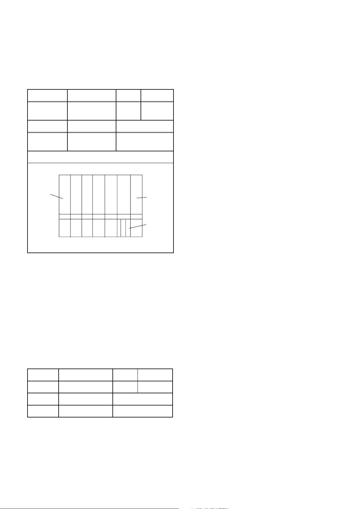
1. Clearance Distance
When replacing primary circuit components, confirm
specified clearance distance (d) and (d') between soldered terminals, and between terminals and surrounding metallic parts. (See Fig. 1)
Table 1 : Ratings for selected area
Chassis or Secondary Conductor
Primary Circuit Terminals
dd’
AC Line Voltage Region
110 to 130 V
Note: This table is unofficial and for reference only.
Be sure to confirm the precise values.
USA or
CANADA
Clearance
Distance (d) (d')
≥ 3.2 mm
(0.126 inches)
2. Leakage Current Test
Confirm the specified (or lower) leakage current between B (earth ground, power cord plug prongs) and
externally exposed accessible parts (RF terminals,
antenna terminals, video and audio input and output
terminals, microphone jacks, earphone jacks, etc.).
Measuring Method : (Power ON)
Insert load Z between B (earth ground, power cord
plug prongs) and exposed accessible parts. Use an
AC voltmeter to measure across both terminals of
load Z. See Fig. 2 and following table.
Table 2 : Leakage current ratings for selected areas
Exposed Accessible Part
Z
One side of
B
Power Cord Plug Prongs
Fig. 1
AC Voltmeter
(High Impedance)
Fig. 2
AC Line Voltage Region Load Z Leakage Current (i) Earth Ground (B) to:
110 to 130 V
Note: This table is unofficial and for reference only. Be sure to confirm the precise values.
USA or
CANADA
0.15µF CAP. & 1.5kΩ
RES. connected in
parallel
1-3-4 TD204IMP
i≤0.5mA rms
Exposed accessible
parts
Page 11
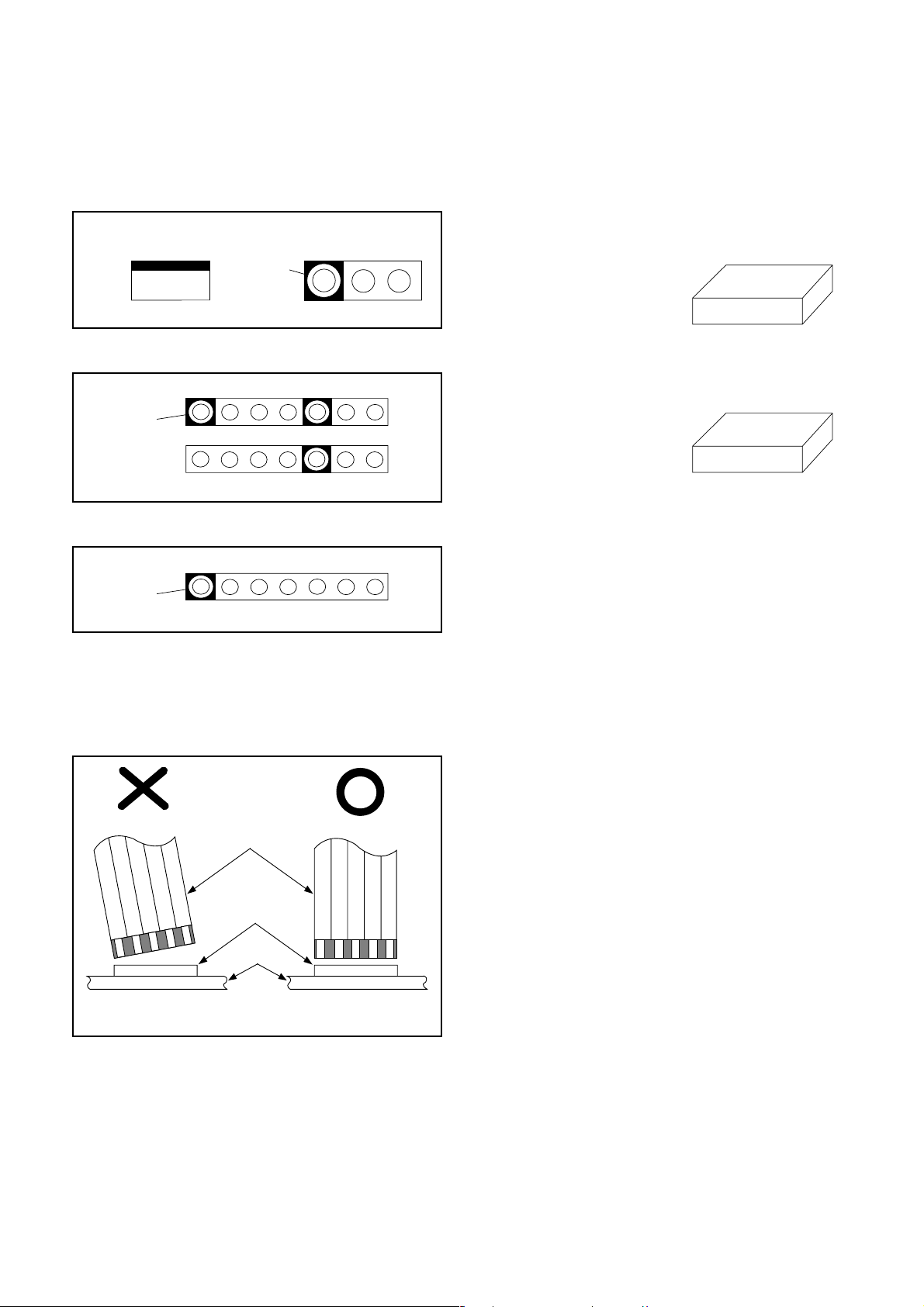
STANDARD NOTES FOR SERVICING
Circuit Board Indications
1. The output pin of the 3 pin Regulator ICs is indicated as shown:
Top View
Out
2. For other ICs, pin 1 and every 5th pin is indicated
as shown:
Pin 1
3. The 1st pin of every pin connector are indicated as
shown:
Pin 1
Input
In
Bottom View
5
10
How to Read the Values of the Rectangular Type Chip Components
Example:
(a) Resistor
473
= 473 = 47 [kΩ]
(b) Capacitor
= Not Shown
Caution:
Once chip parts (Resistors, Capacitors, Transistors,
etc.) are removed, they must not be reused. Always
use a new part.
Replacement Procedures for
(Top View)
(Top View)
Instructions for Connectors
1. When you connect or disconnect FFC cable (connector), be sure to disconnect the AC cord.
2. FFC cable (connector) should be inserted parallel
into the connector, not at an angle.
FFC Cable
Connector
CBA
* Be careful to avoid a short circuit.
[ CBA= Circuit Board Assembly ]
Leadless (Chip) Components
The Following Procedures are Recommended for the Replacement of the
Leadless Components Used in this Unit.
1. Preparation for replacement
a. Soldering Iron
Use a pencil-type soldering iron (less than 30
watts).
b. Solder
Eutectic solder (Tin 63%, Lead 37%) is recommended.
c. Soldering time
Do not apply heat for more than 4 seconds.
d. Preheating
Leadless capacitor must be preheated before
installation. (130°C~150°C, for about two minutes.)
Notes:
a. Leadless components must not be reused after
removal.
b. Excessive mechanical stress and rubbing for the
component electrode must be avoided.
2. Removing the leadless component
Grasp the leadless component body with tweezers
and alternately apply heat to both electrodes. When
the solder on both electrodes has melted, remove
leadless component with a twisting motion.
1-4-1 SFTY_5
Page 12
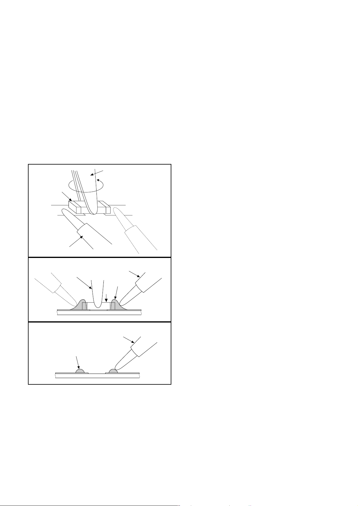
Notes:
a. Do not attempt to lift the component off the board
until the component is completely disconnected
from the board by the twisting action.
b. Take care not to break the copper foil on the
printed board
3. Installing the leadless component
a. Presolder the contact points of the circuit board.
b. Press the part downward with tweezers and solder
both electrodes as shown below.
Note:
Do not glue the replacement leadless component to
the circuit board.
Tweezers
Chip
Soldering Iron
Tweezers
Soldering Iron
Solder
Soldering Iron
2. The Flat Pack-IC on the CBA is affixed with glue,
so be careful not to break or damage the foil of
each pin or solder lands under the IC when removing it.
1. Removal
With Hot - Air Flat Pack - IC Desoldering Machine:
a. Prepare the Hot - Air Flat Pack - IC Desoldering
Machine, then apply hot air to Flat Pack - IC (about
5~6 seconds). (Fig. S-1-1)
b. Remove the Flat Pack- IC with tweezers while
applying the hot air.
With Soldering Iron:
a. Using desoldering braid, remove the solder from all
pins of the Flat Pack - IC. When you use solder flux
which is applied to all pins of the Flat Pack - IC, you
can remove it easily. (Fig. S-1-3)
b. Lift each lead of the Flat Pack - IC upward one by
one, using a sharp pin or wire to which solder will
not adhere (iron wire). When heating the pins, use
a fine tip soldering iron or a hot air Desoldering
Machine. (Fig. S-1-4)
With Iron Wire:
a. Using desoldering braid, remove the solder from all
pins of the Flat Pack - IC. When you use solder flux
which is applied to all pins of the Flat Pack - IC, you
can remove it easily. (Fig. S-1-3)
b. Affix the wire to a workbench or solid mounting
point, as shown in Fig. S-1-5.
c. Pull up on the wire as the solder melts so as to lift
the IC leads from the CBA contact pads, while
heating the pins using a fine tip soldering iron or
hot air blower.
Note:
When using a soldering iron, care must be taken
to ensure that the Flat Pack - IC is not being held
by glue, or when it is removed from the CBA, it
may be damaged if force is used.
Presolder
How to Remove / Install Flat Pack IC
Caution:
1. Do not apply the hot air to the chip parts around the
Flat Pack-IC for over 6 seconds as damage may
occur to the chip parts. Put Masking Tape around
the Flat Pack-IC to protect other parts from damage. (Fig. S-1-2)
2. Installation
a. Using desoldering braid, remove the solder from
the foil of each pin of the Flat Pack - IC on the CBA,
so you can install a replacement Flat Pack - IC
more easily.
b. The "I" mark on the Flat Pack - IC indicates pin 1
(See Fig. S-1-6). Make sure this mark matches the
1 on the CBA when positioning for installation.
Then pre - solder the four corners of the Flat PackIC (See Fig. S-1-7).
c. Solder all pins of the Flat Pack - IC. Make sure that
none of the pins have solder bridges.
1-4-2 SFTY_5
Page 13
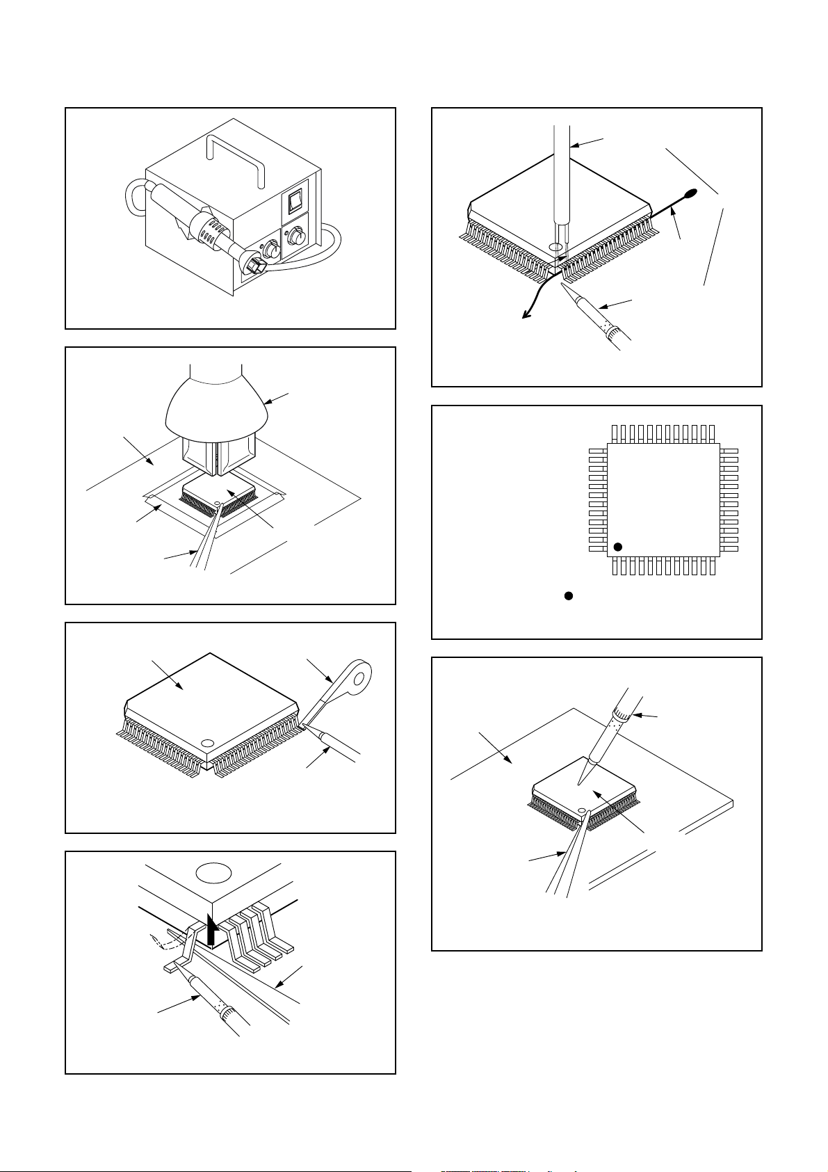
Fig. S-1-1
Hot Air Blower
or
Iron Wire
Soldering Iron
To Solid
Mounting Point
CBA
Masking
Tape
Tweezers
Flat Pack-IC
Fig. S-1-2
Desoldering Braid
Hot-air
Flat Pack-IC
Desoldering
Machine
Flat Pack-IC
Fig. S-1-5
Example :
Pin 1 of the Flat Pack-IC
is indicated by a " " mark.
Fig. S-1-6
CBA
Fine Tip
Soldering Iron
Fine Tip
Soldering Iron
Soldering Iron
Fig. S-1-3
Flat Pack-IC
Tweezers
Fig. S-1-7
Sharp
Pin
Fig. S-1-4
1-4-3 SFTY_5
Page 14
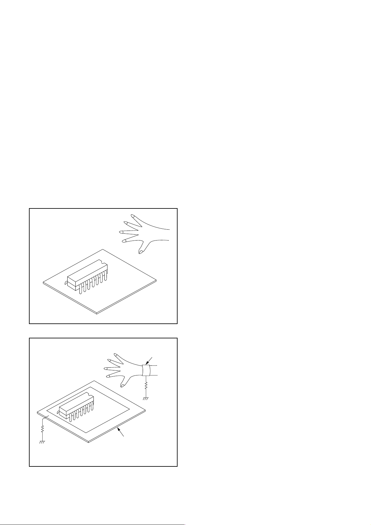
Instructions for Handling
Semiconductors
Electrostatic breakdown of the semiconductors may
occur due to a potential difference caused by electrostatic charge during unpacking or repair work.
Ground for Human Body
Be sure to wear a grounding band (1MΩ) that is properly grounded to remove any static electricity that may
be charged on the body.
Ground for Work Bench
Be sure to place a conductive sheet or copper plate
with proper grounding (1MΩ) on the work bench or
other surface, where the semiconductors are to be
placed. Because the static electricity charge on the
clothing will not escape through the body grounding
band, be careful to avoid contacting semiconductors to
clothing.
<Incorrect>
<Correct>
1MΩ
CBA
Grounding Band
1MΩ
CBA
Conductive Sheet or
Copper Plate
1-4-4 SFTY_5
Page 15
PREPARATION FOR SERVICING
How to Enter the Service Mode
Caution: 1
1. Optical sensors system are used for Tape Start
and End Sensor on this equipment. Read this page
carefully and prepare as described on this page
before starting to service; otherwise, the unit may
operate unexpectedly.
Preparing: 1
1. Cover Q202 (START SENSOR) and Q201 (END
SENSOR) with Insulation Tape or enter the service
mode to activate Sensor Inhibition automatically.
Note: Avoid playing, rewinding or fast forwarding the
tape to its beginning or end, because both Tape End
Sensors are not active.
How to Enter the Service Mode
1. Turn power on.
2. Use service remote control unit and press WAKEUP/SLEEP key. (See page 1-8-1)
3. When entering the service mode, one of the number (1, 2 or 4) will display at corners of the screen.
4. During the service mode, electrical adjustment
mode can be selected by remote control key. (Service remote control unit).
Details are as follows.
Key Adjustment Mode
Picture adjustment mode: Press the
MENU button to change from BRT
(Bright), *CNT (Contrast), *CLR
MENU
0
1 No need to use.
2
3
4
5
(Color), *TNT(Tint) and *V-T. Press
CH UP/DOWN key to display Initial
Value. *Marked items are not necessary to adjust normally.
C-Trap and Y DL Time adjustment
mode: See adjustment instructions
page 1-8-3.
AGC/H adjustment mode: See adjustment instructions page 1-8-2.
Auto AFT adjustment mode: See
adjustment instructions page 1-8-2.
Auto record mode: Perform recording
(15 Sec.)-->Stop-->Rewind (Zero
return) automatically.
Head switching point adjustment
mode: See adjustment instructions
page 1-8-5.
Key Adjustment Mode
6 No need to use.
Purity check mode: Shows Red,
7
8
9
Caution: 2
1. The deck mechanism assembly is mounted on the
Main CBA directly, and SW1211 (REC-SAFETY
SW) is mounted on the Main CBA. When deck
mechanism assembly is removed from the Main
CBA due to servicing, this switch can not be operated automatically.
Green, Blue or White cyclically on the
screen each time the “7” key is
pressed.
H. Shift adjustment mode: See adjustment instructions page 1-8-4.
V.size/V. shift adjustment: See adjustment instructions page 1-8-3.
Preparing: 2
1. To eject the tape, press the STOP/EJECT button
on the unit (or Remote Control).
2. When you want to record during the Service mode,
press the Rec button while depressing SW1211
(REC-SAFETY SW) on the Main CBA.
Q201
(END SENSOR)
SW1211
(REC-SAFETY SW)
Q202
(START SENSOR)
MAIN CBA
1-5-1 TD500PFS
Page 16
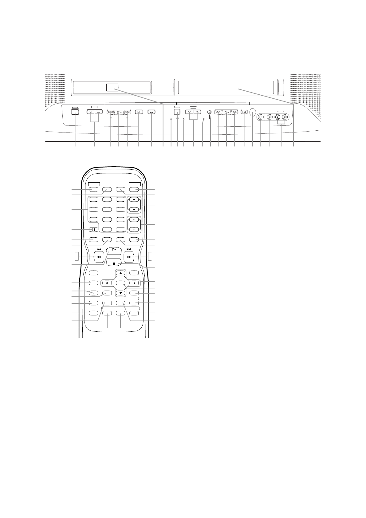
OPERATING CONTROLS AND FUNCTIONS
- TV/DVD/VCR FRONT PANEL -
POWER
VOLUME
DVD buttons TV/VCR buttons
PLAY
SKIP
SKIP
SEARCH
OPEN/CLOSE
STOP
12 4 5 6 107 1514983 3 411 12 13 212019181716
- REMOTE CONTROL -
POWER PICTURE SELECTSLEEP
1
22
23
24
25
26
(DVD) 3
(TV/VCR) 14
4
13
27
28
29
30
31
32
33
1.
POWER button
123
456
789
PAUSE
SPEED C.RESET
RECORD
DISPLAY
CLEAR
MODE
+100
0 +10
PLAY
STOP
ENTER
REPEATSEARCH MODE
RETURNTITLESETUP
CH.
VOL.
MUTEZOOM
DISC
MENU
A
ANGLESUBTITLEAUDIO
-
B
45
44
11
2
43
42
3 (DVD)
15 (TV/VCR)
5
41
40
39
38
37
36
35
34
Press to turn the power on and off.
2. VOLUME X/Y buttons
Press to control the volume level for the DVD and TV.
3. SKIP buttons (for DVD)
Skip chapters or tracks to a desired point.
PLAY button
4.
Starts playback of the disc or tape contents.
5.
STOP button
Stops operation of the disc.
OPEN/CLOSE button
6.
Press to insert discs into or remove them from the
tray.
7.
Disc loading tray
8. DVD indicator
Lights on during DVD mode.
SELECT
CHANNEL
TV/VCR
DVD
9. SELECT button
Press to change to TV/VCR mode or DVD
mode.
NOTE: For about 4 seconds just after the DVD
mode has switched to the TV mode, the button
does not work to switch back to the DVD mode.
10.
TV/VCR indicator
Lights on during TV/VCR mode.
CHANNEL K/L buttons
11.
Press to select memorized channel.
12.
Recording indicator
Flashes during recording. Lights up in the Standby mode for Timer Recording.
REC/OTR (RECORD) button
13.
Press for manual recording. Activates One
Touch Recording. (OTR is only during
TV/VCR mode.)
REW button (for TV/VCR)
14.
Press to rewind the tape, or to view the picture
rapidly in reverse during playback mode.
(Rewind Search)
15.
FWD button (for TV/VCR)
Press to rapidly advance the tape, or to view the
picture rapidly in forward during playback
mode. (Forward Search)
STOP/EJECT button
16.
Press to stop the tape motion. Press in the Stop
mode to remove tape from the unit.
Remote sensor window
17.
18. HEADPHONE jack
To connect headphone (not supplied) for personal listening.
VIDEO input jack
19.
Connect to the video output jack of a video
camera or VCR.
20.
AUDIO L/R input jacks
Connect to the audio output jacks of a video
camera or VCR.
Cassette compartment
21.
22. PICTURE button
Press to adjust the picture.
REC/OTR
REW
HEADPHONE
RL
AUDIO
VIDEO
STOP/EJECT
F.F W D
PLAY
1-6-1 TD500IB
Page 17

- TV/DVD/VCR REAR PANEL -
ANT.
23. Number buttons
TV Mode:
Press two digits to directly access the desired
channel.
Remember to press a "0" before a single digit
channel.
+100 buttonÐ
Press to select cable channels which are equal or
greater than number 100.
DVD Mode:
Press to enter the desired number.
+10 buttonÐ
Press to enter the desired numbers which are
equal or greater than number 10.
PAUSE button
24.
Pauses the current disc or tape operation.
25.
SPEED button
Press to choose the desired recording speed:
SP/SLP.
C.RESET button
26.
Press to reset counter to 0:00:00.
Press to cancel a setting of timer program.
27.
DISPLAY button
TV/VCR Mode:
Display the counter or the current channel number and current time on the TV screen.
DVD Mode:
Displays the current status on the TV screen for
checking purposes.
SETUP button
28.
Press to enter or exit the TV menu or DVD setup
mode.
29.
TITLE button
Displays the title menu.
CLEAR button
30.
Resets a setting.
MODE button
31.
Activates program playback or random playback
mode.
32. SEARCH MODE button
Press to locate a desired point.
AUDIO button
33.
Press to select a desired audio language or sound
mode.
SUBTITLE button
34.
Press to select a desired subtitle language.
1
AUDIO OUT
COAXIAL
L
R
4746 48 49
35.
REPEAT button
Repeats playback of the current disc, title, chapter
or track.
ANGLE button (DVD mode)
36.
Press to change the camera angle to see the
sequence being played back from a different angle.
37. A-B REPEAT button
Repeats playback of a selected section.
RETURN button
38.
Returns to the previous operation.
39.
ENTER button
Press to accept a setting.
40.
Arrow buttons
TV/VCR Mode:
Press to select a setting mode from the menu on
the TV screen.
Press to select or adjust from a particular menu.
DVD Mode:
Use when making settings while watching the
display on a TV screen.
41.
DISC MENU button
Displays the menus in the DVD.
ZOOM Button
42.
Enlarges part of a DVD-reproduced image.
MUTE button
43.
Mutes the sound. Press it again to resume sound.
44.
SLEEP button
Sets the Sleep Timer.
SELECT button
45.
Press to switch TV/VCR and DVD mode. You can
see the mode (TV/VCR or DVD) on the front
panel indicator.
ANT. in jack
46.
Connect to an antenna, cable system, or satellite
system.
Power cord
47.
Connect to a standard AC outlet (120V/60Hz).
NOTE: Remove the power cord from the hook to
avoid breaking a wire before you connect
to a standard AC outlet.
48.
COAXIAL digital audio out jack
Connect to the digital input of an external
amplifier or decoder.
AUDIO L/R output jack
49.
Connect to the analog audio input of an external
amplifier or decoder.
1-6-2 TD500IB
Page 18
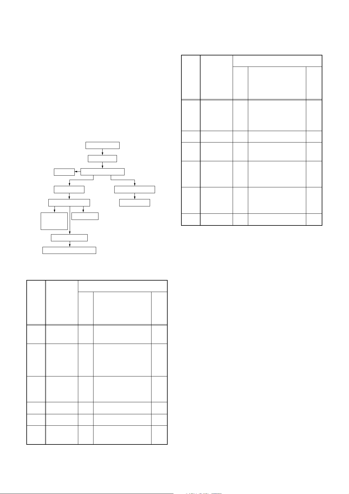
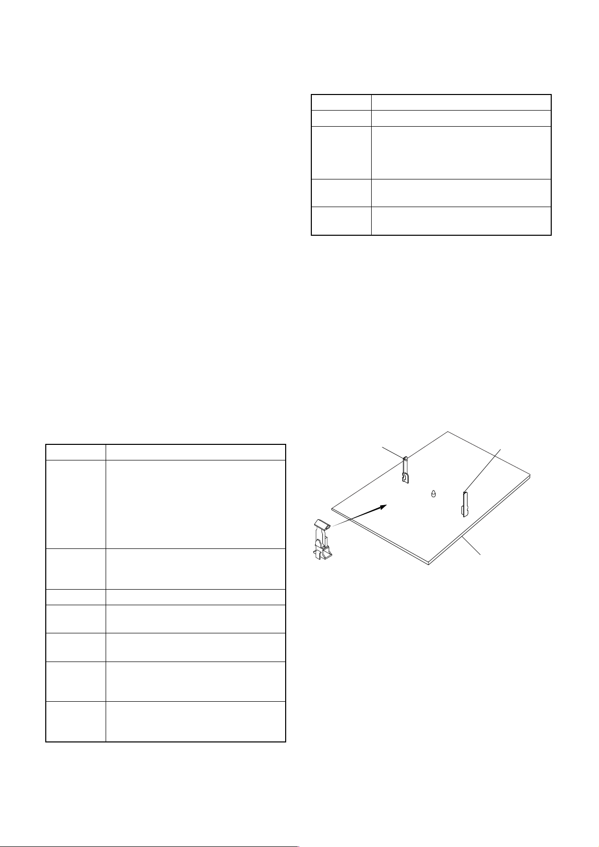
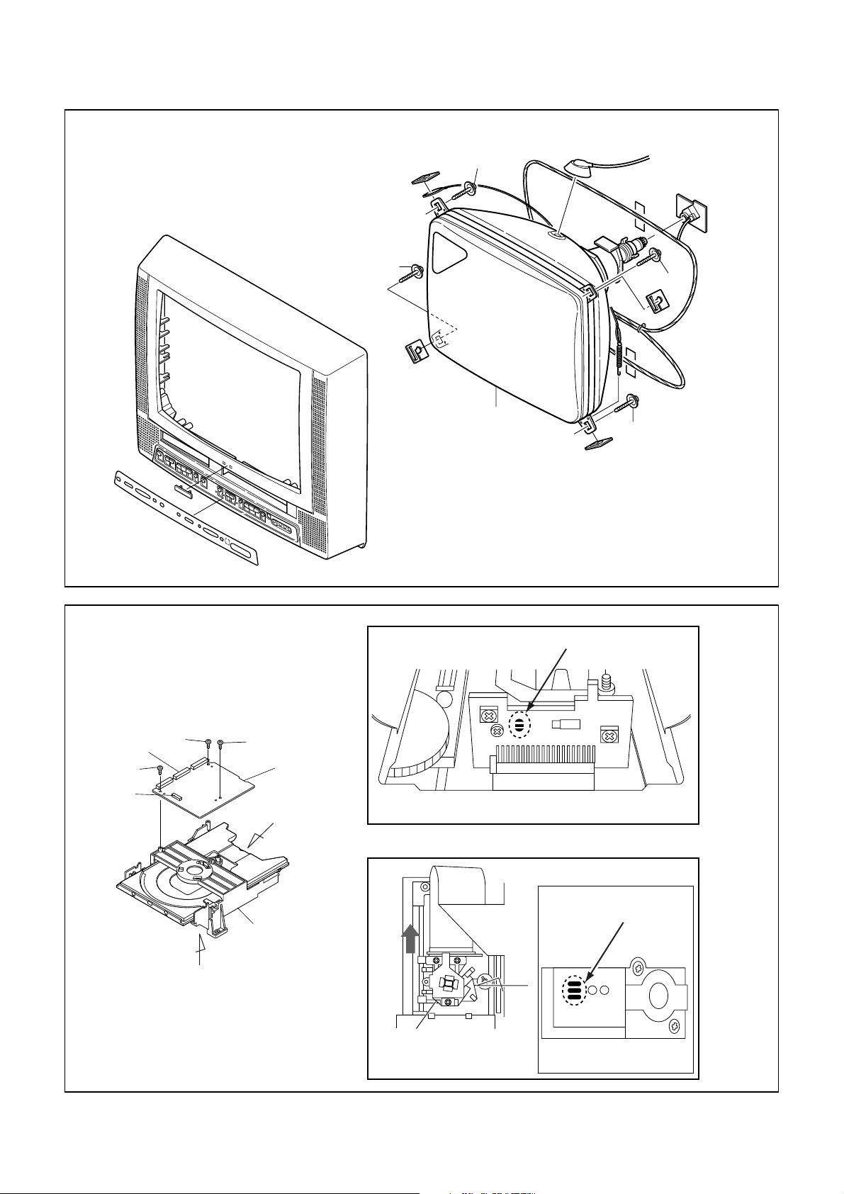
CABINET DISASSEMBLY INSTRUCTIONS
1. Disassembly Flowchart
This flowchart indicates the disassembly steps for the
cabinet parts, and the CBA in order to gain access to
item(s) to be serviced. When reassembling, follow the
steps in reverse order. Bend, route and dress the
cables as they were.
Caution !!
When removing the CRT, be sure to discharge the
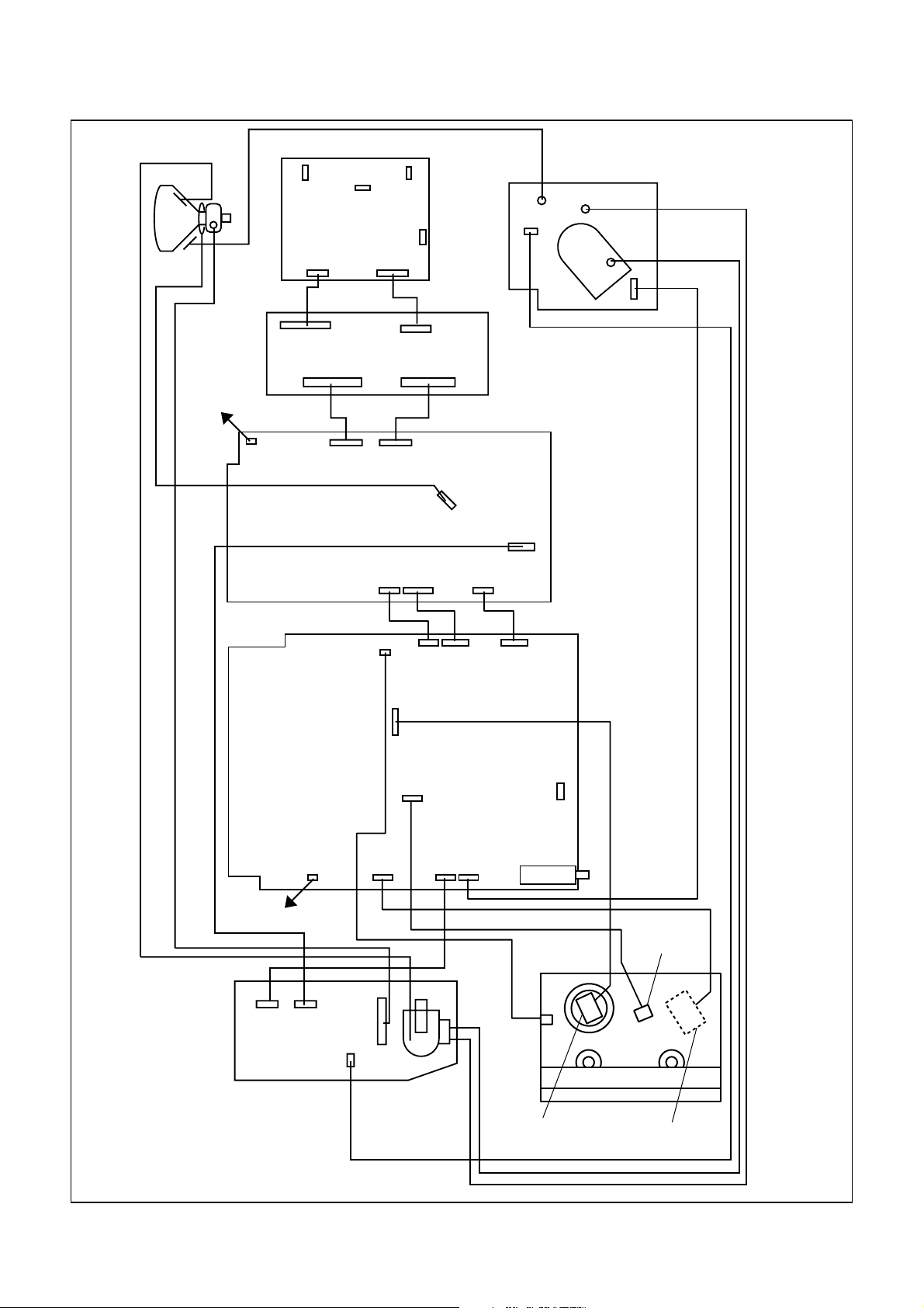
Anode Lead of the CRT with the CRT Ground Wire
before removing the Anode Cap.
[1] Rear Cabinet
[2] H.V. CBA
[4] CRT
[5] Shield Box
[6] DVD Mechanism
MAIN
CBA UNIT
[9] Bottom Plate
[3] Tray Chassis Unit
[11] Deck Assembly
[12] Main CBA
[8] Filter CBA[7] DVD
REMOVAL
ID/
LOC.
No.
PART
REMOVE/
*UNHOOK/UNLOCK/
Fig.
No.
RELEASE/UNPLUG/
DESOLDER
[7]
DVD Main
CBA Unit
3(S-7), CN101,
5
CN401
[8] Filter CBA 3, 6 CN401, CN402 -
Bottom
[9]
[10]
[11]
Plate
Power
Supply/AV
CBA
Deck
Assembly
3 6(S-8) -
3(S-9), CN2802,
3, 6
CN2803, CN2804
7(S-10), 2(S-11),
CL1201, CL1401,
3, 6
CL1402, CL1403
[12] Main CBA 3 3(S-12) -
↓
(1)
↓
(2)
↓
(3)
↓
(4)
Note
2-1
2-2
2-3
3
-
4
↓
(5)
[10] Power Supply/AV CBA
2. Disassembly Method
REMOVAL
ID/
LOC.
PART
No.
Rear
[1]
Cabinet
H.V. CBA
[2]
(With
Holder)
Tray
[3]
Chassis
Unit
[4] CRT 4 4(S-4) -
[5] Shield Box 3 5(S-5) -
REMOVE/
*UNHOOK/UNLOCK/
Fig.
No.
RELEASE/UNPLUG/
DESOLDER
1, 2 6(S-1), 1(S-2), 1(S-3) -
Anode Cap, CN501,
3, 4,
CRT CBA, CN571,
6
CN1301, CN1302,
CN2602
CN1802, CN2801,
3, 6
CN2601
Note
1
-
(1): Order of steps in Procedure. When reassembling,
follow the steps in reverse order.These numbers
are also used as the identification (location) No. of
parts in Figures.
(2): Parts to be removed or installed.
(3): Fig. No. showing Procedure of Part Location.
(4): Identification of part to be removed, unhooked,
unlocked, released, unplugged, unclamped, or
desoldered.
S=Screw, P=Spring, L=Locking Tab, CN=Connec-
tor, *=Unhook, Unlock, Release, Unplug, or
Desolder
2(S-2) = two Screw (S-2)
(5): Refer to the following "Reference Notes in the
Table."
[6]
DVD
Mechanism
CN501, CN701,
3, 6
4(S-6)
-
1-7-1 TD500DC
Page 19

Reference Notes in the Table
Caution !
When removing the CRT, be sure to discharge the
Anode Lead of the CRT with the CRT Ground Wire
before removing the Anode Cap.
Reference Notes in the Table
CAUTION 1: Discharge the Anode Lead of the CRT
with the CRT Ground Wire before removing the Anode
Cap.
1. Disconnect the following: Anode Cap, CN501, CRT
CBA, CN571, CN2602, CN1301 and CN1302.
Then remove H.V. CBA (with Holder).
CAUTION 2: Electrostatic breakdown of the laser
diode in the optical system block may occur as a
potential difference caused by electrostatic charge
accumulated on cloth, human body etc., during
unpacking or repair work.
To avoid damage of pickup follow next procedures.
2-1. Slide the pickup unit as shown in Fig. 5.
2-2. Short the three short lands of FPC cable with sol-
der before removing the FFC cable (CN101) from
it. If you disconnect the FFC cable (CN101), the
laser diode of pickup will be destroyed. (Fig. 5)
2-3. Disconnect Connector (CN401). Remove three
Screws (S-5) and lift the DVD Main CBA Unit.
(Fig. 5)
CAUTION 3: When reassembling, confirm the FFC
cable (CN101) is connected completely. Then remove
the solder from the three short lands of FPC cable.
(Fig. 5)
4. Remove Screws 7(S-10) and 2(S-11). Then, desolder connectors (CL1201, C1401, CL1402, CL1403)
and lift up the Deck Assembly.
1-7-2 TD500DC
Page 20
S-2
S-1
[1] REAR CABINET
S-1 S-1
ANT.
1
S-3
S-1
S-1
S-1
S-1
Fig. 1
S-1
S-3
S-2
S-1
S-1
[1] REAR CABINET
Fig. 2
1-7-3 TD500DC
Page 21
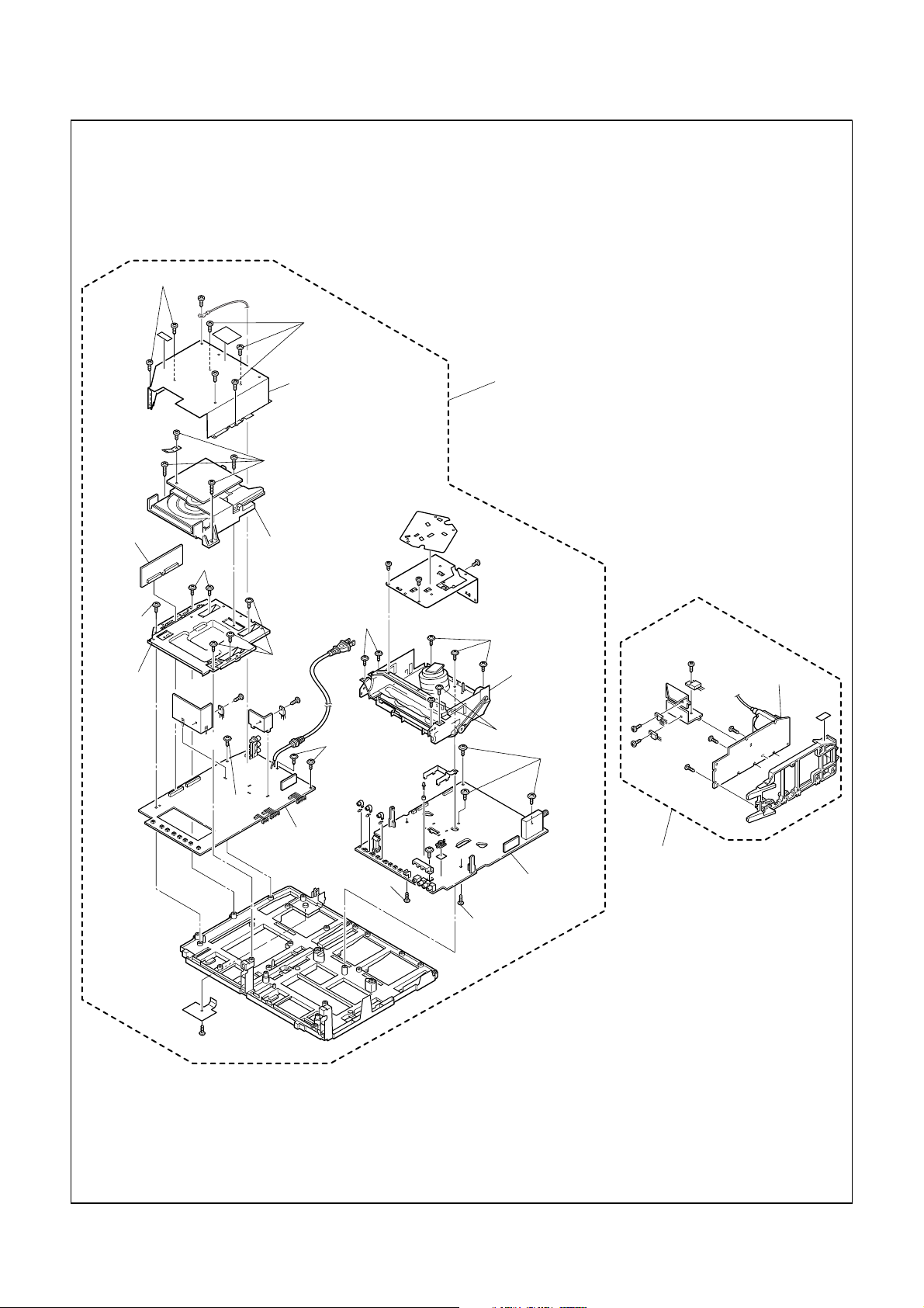
S-5
S-5
[8] Filter
CBA
S-8
[9] Bottom
Plate
S-8
S-9
[5] Shield Box
S-6
[6] DVD
Mechanism
S-8
S-9
S-10
[3] Tray Chassis
S-10
[11] Deck
Assembly
S-10
S-12
H.V. CBA
[10] Power
Supply/
AV CBA
S-11
[2] H.V. CBA
[12] Main CBA
S-11
(wih Holder)
Fig. 3
1-7-4 TD500DC
Page 22
S-4
Anode Cap
S-4
CRT CBA
S-4
CN101
S-7
CN401
S-7
S-7
[7] DVD Main
CBA Unit
A
[4] CRT
S-4
Fig. 4
Short the three short lands by soldering
View for A
OR
Short the three short
lands by soldering
DVD Mechanism
Slide
B
C
Pickup Unit
View for B
View for C
Fig. 5
1-7-5 TD500DC
Page 23
ANODE
CRT
DVD MAIN CBA
FACTORY USE
ONLY
CL501
CRT CBA
CN501
SCREEN
GND
TO
SPEAKER
CN2801
POWER SUPPLY/
AV CBA
CN501
CN403
CN401
CN2401 CN2402
CN2802
CL1403
CN701
CN404
CN1805
CN402
CN2803
CN2601
CN2804
CN1804
FOCUS
CL504A
FILTER CBA
CN2602
CN1803
H.V. CBA
MAIN CBA
CN1802
TO SPEAKER
CL503A
CL501A
CL502A
CN571
CL1201
CL1401
CL1402
CN1302
INT MON
FACTORY USE
ONLY
CN1301
CN1303
TUNER
FE HEAD
CYLINDER
ASSEMBLY
AC HEAD
ASSEMBLY
DECK ASSEMBLY
CAPSTAN
MOTOR
Fig. 6
1-7-6 TD500DC
Page 24
ELECTRICAL ADJUSTMENT INSTRUCTIONS
General Note:
"CBA" is abbreviation for "Circuit Board
Assembly."
NOTE:
Electrical adjustments are required after replacing
circuit components and certain mechanical parts.
It is important to perform these adjustments only
after all repairs and replacements have been completed.
Also, do not attempt these adjustments unless the
proper equipment is available.
Test Equipment Required
1. NTSC Pattern Generator (Color Bar W/White Window, Red Color, Dot Pattern, Gray Scale,
Monoscope, Multi-Burst)
2. AC Milli Voltmeter (RMS)
3. Alignment Tape (FL8A, FL8N), Blank Tape
4. DC Voltmeter
5. Oscilloscope: Dual-trace with 10:1 probe,
V-Range: 0.001~50V/Div,
F-Range: DC~AC-60MHz
6. Frequency Counter
7. Plastic Tip Driver
How to Set up the Service mode:
Service Mode:
1. Use the service remote control unit.
2. Turn the power on. (Use main power on the TV
unit.)
3. To enter the TV mode, press CH UP or CH DOWN
button on the TV unit.
4. Press "DISC MENU" button on the service remote
control unit. (Version of micro computer will display
on the CRT. (Ex: 057-001)
X-Ray Protection Test
X-Ray protection test should be done when replacing
any parts of this chassis.
1. Short test points J551 and J552 (on H.V. CBA).
2. Confirm that the main power turns off.
3. If the main power does not turn off, then replace
the following parts (D591, Q591, R592, R593,
R594 and IC1201).
4. Perform steps 1 to 3 again.
1. DC 114V (+B) Adjustment
Purpose: To obtain correct operation.
Symptom of Misadjustment: The picture is dark and
unit does not operate correctly.
How to make service remote control
unit:
1. Prepare normal remote control unit. (Part No.
NE200UD) Remove 4 screws from the back lid.
(Fig. 1-1)
2. Add J1 (Jumper Wire) to the remote control CBA.
(Fig. 1-2)
SCREW
Remote control unit (Bottom)
J 1
Fig. 1-1
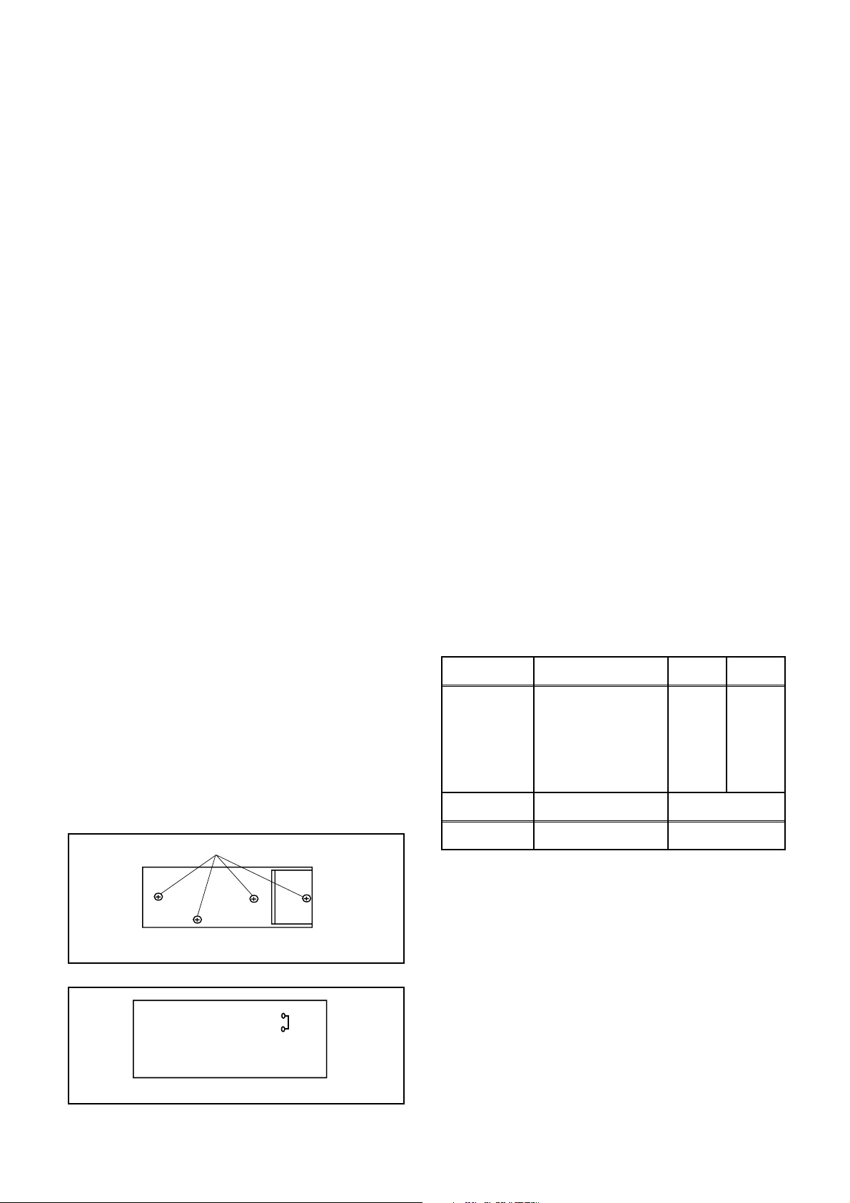
Test point Adj. Point Mode Input
J533
(+B)
HEAT SINK
(on H.V.
CBA)
(GND)
Tape M. EQ. Spec.
--- DC Voltmeter +114±0.5V DC
Note: J533(+B), HEAT SINK --- H.V. CBA
,VR2601 --- Power Supply/AV CBA
1. Connect the unit to AC Power Outlet.
2. Connect DC Volt Meter to J533(+B) and HEAT
SINK (on H.V. CBA)(GND).
3. Adjust VR2601 so that the voltage of J533(+B)
becomes +114±0.5V DC.
VR2601 --- -----
Remote control CBA
Fig. 1-2
1-8-1 TD500EA
Page 25

2. Auto AFT (VCO) Adjustment
4-1. H Adjustment
Purpose: To operate AFT correctly.
Symptom of Misadjustment: AFT does not work cor-
rectly and/or synchronization is faulty.
Test point Adj. Point Mode Input
--- --- Video -----
Tape M. EQ. Spec.
--- --- ---
1. Set the unit to the Video mode with no signal input.
2. Enter the Service mode. (See page 1-8-1.) Then
press number "3" button on the remote control unit.
3. If the screen color changes to "Green" then this
adjustment is finished.
4. If the screen color changes to "Red" then this
adjustment is failed. Repeat steps 1 and 2 or check
relative circuit or parts (IC).
3. TV AGC Adjustment
Purpose: Set AGC (Auto Gain Control) Level.
Symptom of Misadjustment: AGC does not synchro-
nize correctly when RF input level is too weak and picture distortion may occur if it is too strong.
Test point Adj. Point Mode Input
Purpose: To get correct horizontal position and size
of screen image.
Symptom of Misadjustment: Horizontal position and
size of screen image may not be properly displayed.
Test point Adj. Point Mode Input
R583
Tape M. EQ. Spec.
--- Frequency Counter 15.734kHz±300Hz
Note: R583 --- H.V. CBA
1. Connect Frequency Counter to R583.
2. Operate the unit for at least 20 mintes.
3. Enter the Service mode. (See page 1-8-1.) Press
"2" button on the remote control unit and select HADJ Mode. (Press "2" button then display will
change H-ADJ and AGC.)
4. Press CH o / p buttons on the remote control unit
so that the display will change "0" to "7."
5. At this moment, choose display "0" to "7" when the
Frequency counter display is closest to
15.734kHz±300Hz.
6. Turn the power off and on again.
CH o / p
buttons
Video ---
TP1001
Tape M. EQ. Spec.
---
Note: TP1001--- Main CBA
1. Enter the Service mode. (See page 1-8-1.) Then
press number 2 button on the remote control unit.
2. Receive the Color Bar signal for channel 4
(67.25MHz). (RF Input Level: 60dBµV)
3. Press CH. o / p buttons so that the voltage of
TP1001 (AGC) becomes +2.8V±0.3V DC.
4. Turn the power off and on again.
CH. o / p
buttons
Pattern Generator
DC Voltmeter
---
+2.8±0.3V DC
Color Bar
67.25MHz
60dBµV
1-8-2 TD500EA
Page 26
4-2. C-Trap Adjustment
5. V. Size Adjustment
Purpose: To get minimum leakage of the color signal
carrier.
Symptom of Misadjustment: If C-Trap Adjustment is
incorrect, stripes will appear on the screen.
Test point Adj. Point Mode Input
D1304
(Cathode)
(B-OUT)
Tape M. EQ. Spec.
---
minimum
CH o / p
buttons
Oscilloscope
Pattern Generator
Figure
--- Color Bar
---
Fig. 2
Purpose: To obtain correct vertical height of screen
image.
Symptom of Misadjustment: If V. Size is incorrect,
vertical height of image on the screen may not be
properly displayed.
Test point Adj. Point Mode Input
---
Tape M. EQ. Spec.
--- Pattern Generator 90±5%
1. Enter the Service mode. (See page 1-8-1.)
Press "9" button on the remote control unit and
select V-S Mode. (Press "9" button then display will
change to V-P and V-S).
2. Input monoscope pattern.
3. Press CH o / p buttons on the remote control unit
so that the monoscope pattern is 90±5% of display
size and the circle is round.
CH o / p
buttons
--- Monoscope
6. V. Shift Adjustment
Note: D1304 (Cathode) (B-Out)--- Main CBA
1. Connect Oscilloscope to D1304 (Cathode).
2. Input a color bar signal from RF input.
Enter the Service mode. (See page 1-8-1.)
3. Press "0" button on the remote control unit and
select C-TRAP Mode.
4. Press CH o / p buttons on the remote control unit
so that the carrier leakage B-Out (3.58MHz) value
becomes minimum on the oscilloscope.
5. Turn the power off and on again.
Purpose: To obtain correct vertical position of screen
image.
Symptom of Misadjustment: If V. position is incorrect, vertical position of image on the screen may not
be properly displayed.
Test point Adj. Point Mode Input
---
Tape M. EQ. Spec.
--- Pattern Generator ---
1. Enter the Service mode. (See page 1-8-1.)
Press "9" button on the remote control unit and
select V-P Mode. (Press "9" button then display will
change to V-P and V-S).
2. Input monoscope pattern.
3. Press CH o / p buttons on the remote control unit
so that the top and bottom of the monoscope pattern are equal to each other.
CH o / p
buttons
--- Monoscope
1-8-3 TD500EA
Page 27
7. H. Shift Adjustment
Purpose: To obtain correct horizontal position and
size of screen image.
Symptom of Misadjustment: Horizontal position and
size of screen image may not be properly displayed.
Test point Adj. Point Mode Input
---
Tape M. EQ. Spec.
--- Pattern Generator ---
1. Enter the Service mode. (See page 1-8-1.)
Press "8" button on the remote control unit and
select H-P Mode.
2. Input monoscope pattern.
3. Press CH o / p buttons on the remote control unit
so that the left and right side of the monoscope pattern are equal to each other.
4. Turn the power off and on again.
CH o / p
buttons
--- Monoscope
8. Cut-off Adjustment
Purpose: To adjust the beam current of R, G, B, and
screen voltage.
Symptom of Misadjustment: White color may be
reddish, greenish or bluish.
Test point Adj. Point Mode Input
Black
--- Screen-Control Ext.
Raster /
White
Raster
Notes: Screen Control FBT --- H.V. CBA
FBT= Fly Back Transformer
Use the Remote Control Unit
1. Degauss the CRT and allow CRT to operate for 20
minutes before starting the alignment.
2. Set the screen control to minimum position. Input
the Black raster signal from RF input.
3. Enter the Service Mode. (See page 1-8-1.)
Dimmed horizontal line appears on the CRT.
4. Press the "VOL p" button.
(Press "VOL p" then display will change CUT OFF/
DRIVE, VCO adjustment, 7Fh adjustment).
5. Choose CUT OFF/DRIVE Mode then press "1" button. This adjustment mode is CUT OFF (R).
6. Press the "CH o / p" button until the horizontal line
becomes white.
7. Choose CUT OFF/DRIVE mode then press "2" button. This adjustment mode is CUT OFF (G). Press
"CH o / p" until the horizontal line becomes white.
8. Choose CUT OFF/DRIVE mode then press "3" button. This adjustment mode is CUT OFF (B). Press
"CH o / p" until the horizontal line becomes white.
9. Input the White Raster Signal from Video In.
10.Choose CUT OFF/DRIVE mode then press "4."
Adjust the RED DRIVE as needed with the CH o /
p buttons to get the following value, X= 286, Y=
294.
11.Choose CUT OFF/DRIVE mode then press "5."
Adjust the BLUE DRIVE as needed with the CH o /
p buttons to get the following value, X= 286.
12.Turn the power off and on again.
Tape M. EQ. Spec.
--- Pattern Generator
Figure
PATTERN GENERATOR
RF INPUT
See Reference
Notes below
Fig. 3
1-8-4 TD500EA
Page 28
9. Sub-Brightness Adjustment
Purpose: To get proper brightness.
Symptom of Misadjustment: If Sub-Brightness is
incorrect, proper brightness cannot be obtained by
adjusting the Brightness Control.
Test point Adj. Point Mode Input
---
Tape M. EQ. Spec.
CH o / p
buttons
---
SYMPTE
7.5IRE
3. Input the monoscope pattern.
4. Adjust the Focus Control on the FBT to obtain clear
picture.
11. SIF Adjustment
Purpose: To set the SIF (Sound Intermediate Fre-
quency).
Symptom of Misadjustment: Audio may not sound
correctly.
Note: This adjustment automatically done by the
chrominance IC (IC1301).
---
White
Note: SYMPTE Setup level --- 7.5 IRE
1. Enter the Service Mode. (See page 1-8-1.)
Then input SYMPTE signal from RF input.
2. Press MENU button. (Press MENU button then display will change B R T, C N T, T N T, V-T and
SHP). Select BRT and press CH o / p buttons so
that the bar is just visible (See above figure).
3. Turn the power off and on again.
Pattern
Generator
Figure
See below
Black
This bar
just
visible
Fig. 4
10. Focus Adjustment
Purpose: Set the optimum Focus.
Symptom of Misadjustment: If Focus Adjustment is
incorrect, blurred images are shown on the display.
12. CCS Text Box Location
When replacing the CRT, the CCS Box might not stay
in appropriate position. Then, replace micro computer.
Note: This adjustment automatically done by the
microcomputer.
13. Head Switching Position Adjustment
Purpose: Determine the Head Switching Point during
Playback.
Symptom of Misadjustment: May cause Head
Switching Noise or Vertical Jitter in the picture.
Note: Unit reads Head Switching Position automatically and displays it on the screen (Upper Left Corner).
1. Playback test tape (FL8A, FL8N).
2. Enter the Service Mode. (See page 1-8-1.)
Then press the number 5 button on the remote
control unit.
3. The Head Switching position will display on the
screen; if adjustment is necessary follow step 4.
6.5H(412.7µs) is preferable.
4. Press "CH o" or "CH p" button on the remote control unit if necessary. The value will be changed in
0.5H steps up or down. Adjustable range is up to
9.5H. If the value is beyond adjustable range, the
display will change as:
Lower out of range: 0.0H
Upper out of range: -.-H
5. Turn the power off and on again.
Test point Adj. Point Mode Input
--- Focus Control --- Monoscope
Tape M. EQ. Spec.
--- Pattern Generator See below.
Note: Focus VR (FBT) --- H.V. CBA
FBT= Fly Back Transformer
1. Operate the unit more than 30 minutes.
2. Face the unit to the East and degauss the CRT
using a Degaussing Coil.
1-8-5 TD500EA
Page 29
The following 2 adjustments normally are not
attempted in the field. They should be done
only when replacing the CRT then adjust as a
preparation.
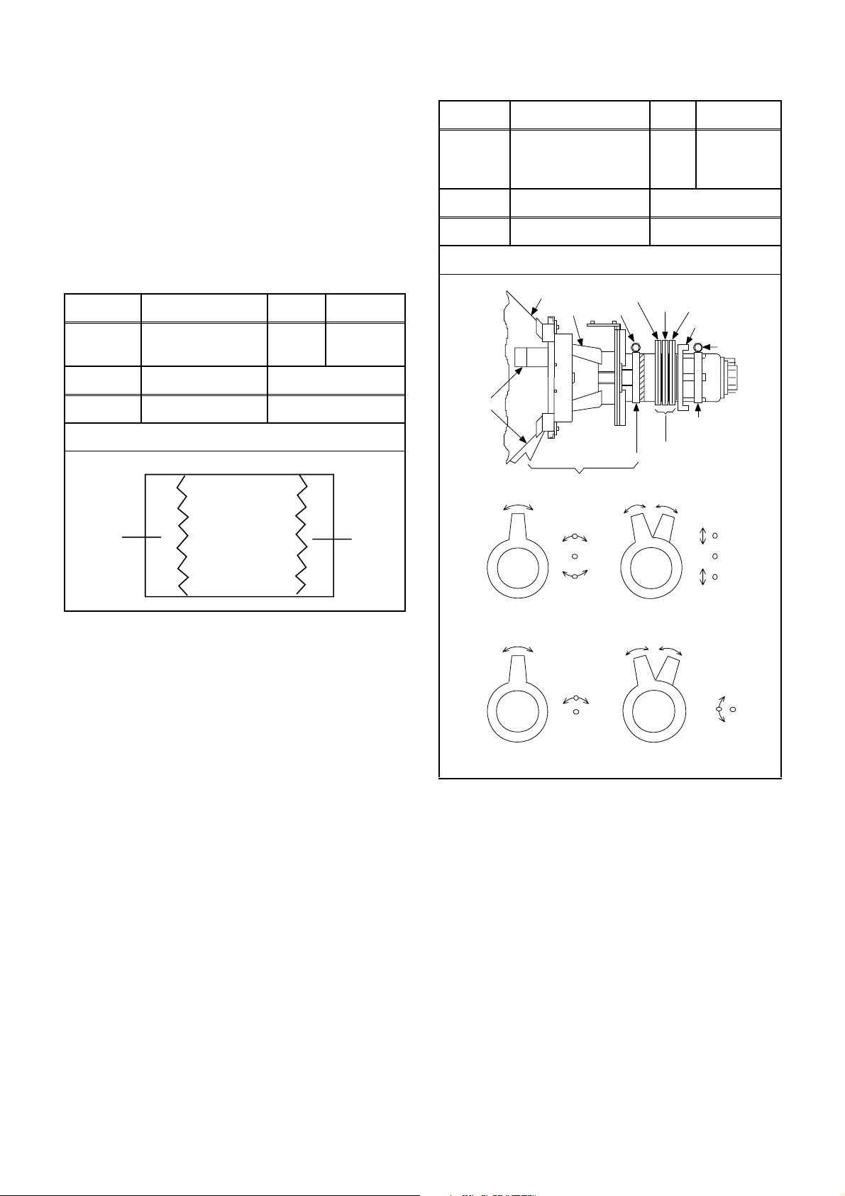
14. Purity Adjustment
Purpose: To obtain pure color.
Symptom of Misadjustment: If Color Purity Adjust-
ment is incorrect, large areas of color may not be
properly displayed.
Test point Adj. Point Mode Input
---
C.P. Magnet (RB),
C.P. Magnet (RB-G),
Deflection Yoke
---
Dot Pattern
or
Crosshatch
Tape M. EQ. Spec.
--- Pattern Generator See below.
Figure
Test point Adj. Point Mode Input
---
Deflection Yoke
Purity Magnet
--- Red Color
Tape M. EQ. Spec.
--- Pattern Generator See below.
Figure
GREEN
RED
BLUE
Fig. 5
1. Set the unit facing east.
2. Operate the unit for over 30 minutes before adjusting.
3. Fully degauss the unit using an external degaussing coil.
4. Set the unit to the AUX Mode which is located
before CH2 then input a red raster from video in.
5. Loosen the screw on the Deflection Yoke Clamper
and pull the Deflection Yoke back away from the
screen. (See Fig. 6.)
6. Loosen the Ring Lock and adjust the Purity Magnets so that a red field is obtained at the center of
the screen. Tighten Ring Lock. (See Fig. 5,6.)
7. Slowly push the Deflection Yoke toward the bell of
the CRT and set it where a uniform red field is
obtained.
8. Tighten the clamp screw on the Deflection Yoke.
15. Convergence Adjustment
Purpose: To obtain proper convergence of red, green
and blue beams.
Symptom of Misadjustment: If Convergence Adjustment is incorrect, the edge of white letters may have
color edges.
CRT
COIL
DY WEDGE
COIL CLAMPER
DEFLECTION YOKE
PURITY
SCREW
RB
RB-G
RING LOCK
C.P. MAGNET
CLAMPER
C.P. MAGNET
SCREW
Fig. 6
C.P. MAGNET (RB)
R
G
B
R
G
B
Fig. 7
C.P. MAGNET (RB-G)
RB
RB
G
G
Fig. 8
1. Set the unit to the AUX Mode which is located
before CH2 then input a Dot or crosshatch pattern.
2. Loosen the Ring Lock and align red with blue dots
or Crosshatch at the center of the screen by rotating (RB) C.P. Magnets. (See Fig. 7.)
3. Align red / blue with green dots at the center of the
screen by rotating (RB-G) C.P. Magnet.
(See Fig. 8.)
4. Fix the C.P. Magnets by tightening the Ring Lock.
5. Remove the DY Wedges and slightly tilt the Deflection Yoke horizontally and vertically to obtain the
best overall convergence.
6. Fix the Deflection Yoke by carefully inserting the
DY Wedges between CRT and Deflection Yoke.
1-8-6 TD500EA
Page 30
FIRMWARE RENEWAL MODE
HOW TO UPDATE THE FIRMWARE
VERSION
1. Turn the power on and remove the disc on the tray.
2. To enter the DVD mode, press [SELECT] button on
the remote control unit. (DVD indicator lights on.)
3. To open the tray, press [OPEN/CLOSE] button on
the remote control unit.
4. To put the unit into version up mode, press [9], [8],
[7], [6], and [SEARCH MODE] buttons on the
remote control unit in that order. The tray will open
automatically.
Fig. A appears on the screen .
BE F/W VERSION UP MODE
PLEASE INSERT A DISC
FOR BE F/W VERSION UP.
The appearance shown in (*2) of Fig. B is
described as follows:
AppearanceNo. State
Reading... Sending files into the memory
1
Erasing... Erasing previous version data
2
Programming...
3 Writing new version data
7. After programming is finished, the tray opens automatically. Fig. C appears on the screen
BE F/W VERSION UP MODE
VERSION: ********
COMPLETED SUM:7abc(*3)
SELECT
EXIT:
Fig. A Version Up Mode Screen
The unit can also enter the version up mode with
the tray open. In this case, Fig. A will be shown on
the screen while the tray is open.
5. Load the disc for version up. (For closing the tray,
only the [OPEN/CLOSE] button is available.)
6. The unit enters the F/W version up mode automatically. Fig. B appears on the screen.
BE F/W VERSION UP MODE
VERSION: ********
Reading...(*2)
Fig. C Completed Program Mode Screen
At this time, no buttons are available.
8. For tray opening, plug the AC cord into the AC outlet.
9. To close the tray, press [POWER] and [SELECT]
buttons on the remote control unit or [SELECT] button on the unit.
HOW TO VERIFY THE FIRMWARE
VERSION
1. After making sure that no disc is in unit, turn the
power on.
2. Press [1], [2], [3], [4], and [DISPLAY] buttons on
the remote control unit in that order. The F/E and
B/E versions appear on the screen.
Fig. B Programming Mode Screen
1-9-1 TD601ROM
Page 31

Servo/System Control Block Diagram
SW2406 SW2408
SW2401 SW2405
FROM/TO
DVD
SYSTEM
CONTROL
BLOCK
DIAGRAM
CN401
CN2401
3 SCLK
4 CS
5 REMOTE
POWER SUPPLY / AV CBA
(DECK ASSEMBLY)
KEY SWITCH
KEY SWITCH
CN2802
6 6KEY1
5 5KEY2
CN2803
112 SDATA
12
13
15
CN1805
CN1804
11SDATA
12SCLK
13CS
15REMOTE
BLOCK DIAGRAMS <TV/VCR Section>
IC1201
(SERVO/SYSTEM CONTROL)
MAIN CBA
SW1201 SW1203,
SW1206 SW1210
KEY SWITCH
AL+5V
P-ON+5V
D1224 S-LED
D1204 REC
Q1207
D1216 DVD
D1217
TV/VCR
Q1211
AL+5V
KEY0
5
KEY1
6
KYE2
8
SDATA
52
51
SCLK
50
CS
25
REM-OUT
REC-LED
21
DVD-H
48
TV/VCR-LED
26
REMOTE
SCL
SDA
I2C-OPEN
REC-SAFETY
C-SYNC
14
71
72
45
33
74
RS1201
REMOTE
SENSOR
SW1211
REC
SAFETY
IC1202
SCL
6
5
SDA
CS
7
I2C-OPEN
C-SYNC
(MEMORY)
SCL
SDA
EXT-H
DVD-H
FROM/TO
CHROMA
/TUNER
BLOCK
DIAGRAM
AC HEAD ASSEMBLY
CONTROL
HEAD
CYLINDER ASSEMBLY
PG
SENSOR
DRUM
MOTOR
M
LOADING
MOTOR
M
CL1402
5CTL(+)
6CTL(-)
Q202
ST-SENS.
SENSOR CBA
(ST-SENSOR)
CAPSTAN MOTOR
CAPSTAN
MOTOR
M
Q201
END-SENS.
SENSOR CBA
(END-SENSOR)
P-ON+5V
C-FG
CL1201
1C-F/R
2AL+12V
3D/L+12V
4
5FG-GND
6
7C-CONT
8M-GND
9D-FG
10LD-CONT
11D-CONT
12D-PG
Q1206
T-REEL
AL+12V
D/L+12V
P-ON+5V
Q1210
WF3
TP1201
CTL-AMP-OUT
SW1212
LD-SW
Q1205
RESETT+5V
AL+5V
CTL(+)
95
94
CTL(-)
CTL AMP-OUT
97
LD-SW1
9
ST-SENS.
7
END-SENS.
T-REEL
80
RESET
34
66
C-F/R
87
C-FG
76
C-CONT
89
D-FG
82
LD-CONT
77
D-CONT
90
D-PG
DVD-MAIN-PWR
P-ON-H
P-DOWN-L
Hi-Fi-CS
Hi-Fi-DATA
Hi-Fi-CLK
ST/SAP-IN
NORMAL-H
Hi-Fi-SW
DVD-MUTE
JACK-MUTE-H
A-MUTE-H
D-REC-H
VOL-CONT
V-H-SW
ENV-DET
REC/EE/PB
DV-SYNC
V-ENV
ROTA
RF-SW
TAPE-SPEED
EXT-H
RENTAL
SPL-PLAY
42
31
84
69
68
70
22
19
73
67
65
44
11
16
17
27
13
10
15
18
28
29
30
32
DVD-MAIN-PWR
P-ON-H
P-DOWN-L
Hi-Fi-CS
Hi-Fi-DATA
Hi-Fi-CLK
4
ST/SAP-IN
NORMAL-H
Hi-Fi-SW
A-MUTE-H
DVD-MUTE
JACK-MUTE-H
A-MUTE-H
D-REC-H
VOL-CONT
EXT-H
DVD-H
V-H-SW
ENV-DET
REC/EE/PB
DV-SYNC
V-ENV
ROTA
RF-SW
TAPE-SPEED
EXT-H
RENTAL
SPL-PLAY
FROM/TO
POWER
SUPPLY BLOCK
DIAGRAM
FROM/TO
Hi-Fi AUDIO
BLOCK
DIAGRAM
FROM/TO
AUDIO BLOCK
DIAGRAM
FROM/TO
VIDEO BLOCK
DIAGRAM
1-10-1 1-10-2 TD500BLS
Page 32

Video Block Diagram
REC VIDEO SIGNAL PB VIDEO SIGNAL MODE: SP/REC
FROM/TO
CHROMA/
TUNER BLOCK
DIAGRAM
VCR-VIDEO
VIDEO
WF5
TP1402
V-OUT
WF4
IC1401
VIDEO/AUDIO
SIGNAL PROCESS
42
42
38
Q1401
BUFFER
V-AGC
35
6dB
AMP
CHARA
MIX
FBC
R P
X1401
3.58MHz
62 61
VXO
WF2
Y/C
MIX
MAIN CBA
45 47 49 44
CCD 1H
DELAY
DOC YNR Y/C COMB
Q1402
BUFFER
LUMINANCE
SIGNAL PROCESS
FROM
SERVO/SYSTEM
CONTROL BLOCK
DIAGRAM
(DECK ASSEMBLY)
EXT-H
RENTAL
REC/EE/PB
SPL-PLAY
ROTA
DV-SYNC
TAPE-SPEED
CYLINDER ASSEMBLY
VIDEO (R)-1 HEAD
VIDEO (L)-1 HEAD
VIDEO (L)-2 HEAD
VIDEO (R)-2 HEAD
71
36
RENTAL
REC/EE/PB
16
SPL-PLAY
73
ROTA
14
DV-SYNC
39
TAPE-SPEED
59
CL1401
V(R)-1
9
V-COM
8
V(L)-1
7
V(L)-2
6
V-COM
5
V(R)-2
4
FROM/TO
SERVO/SYSTEM
CONTROL BLOCK
DIAGRAM
WF1
RF-SW
V-ENV
V-H-SW
ENV-DET
TP1401
RF-SW
91
90
89
88
85
84
83
82
13
93
15
94
ENV-DET
CHROMINANCE
SIGNAL PROCESS
R
L
L
R
SP
EP
HPF
AGC
AMP
R
P
ENV
DET
74
TP1403
ENV
WF6
1-10-3 1-10-4 TD500BLV
Page 33

Audio Block Diagram
REC-AUDIO SIGNAL
PB-AUDIO SIGNAL
DVD AUDIO SIGNAL DATA(AUDIO) SIGNAL
Mode : SP/REC
FROM DVD AUDIO
BLOCK DIAGRAM
CN402
FROM
Hi-Fi AUDIO
BLOCK
DIAGRAM
FROM
SERVO/
SYSTEM
CONTROL
BLOCK DIAGRAM
CN1804
7
5
A-OUT(R)5 5
A-OUT(L)3 3
DVD-H19 19
CN2402
SPDIF11
DVD-AUDIO(R)
DVD-AUDIO(L)
DVD-MUTE13
CN2803
CN2803CN1804
POWER SUPPLY / AV CBA
Q2205
BUFFER
IC2203
(OP AMP)
5
3 1
Q2207
7
2
1
12
13
Q2203
IC2202
(OUTPUT SELECT)
15
14
SW CTL.
1110
Q2209
P-ON+5V
IC2801
(AUDIO AMP)
5
2 12
DC VOL.
6
Q2204
Q2202
Q2208
VOLUME
JACK-MUTE-H
DVD-MUTE
7
JK2201
DIGITAL
A-OUT
A-OUT(R)
A-OUT(L)
FROM/TO
SERVO/SYSTEM
CONTROL BLOCK
DIAGRAM
CN2801
SP-L
SP-GND 2
CN1805CN2802
A-OUT(R)10 10
A-OUT(L)9 9
SP-L11 11
1
SP2801
SPEAKER
L-CH
CN1802
SP-R
SP-GND 2
1
SP1801
SPEAKER
R-CH
JK1801
HEADPHONE
JACK
FROM/TO
Hi-Fi AUDIO
BLOCK
DIAGRAM
N-A-IN
N-A-OUT
BLOCK DIAGRAM FOR SECTION 2 (DECK MECHANISM)
AC HEAD ASSEMBLY
AUDIO
HEAD
AUDIO
ERASE
HEAD
FE HEAD UNIT
FULL
ERASE
HEAD
CL1402
A-PB/REC
4
A-COM
3
AE-H
1
AE-H/FE-H
2
CN1403
FE-H
1
FE-H GND
2
Q1873
Q1874
Q1872
BIAS
OSC
Q1875
Q1871
P-ON+5V
P-ON+5V
76
78
80
4
99
IC1401
(AUDIO PROCESS)
EQ
AMP
3
AUTO
BIAS
SP/LP-ON
ALC
REC
AMP
LINE
AMP
11
EXT-H
96
98
FROM SERVO/SYSTEM
CONTROL BLOCK
DIAGRAM
MUTE
D-REC-H
EXT-H
7112
A-MUTE-H
D-REC-H
R
1
2
6
100
P
7
WF8
WF7
TP1802
NA-IN-YCA
1-10-5
MAIN CBA
TD500BLA1-10-6
Page 34

Hi-Fi Audio Block Diagram
FROM
CHROM/TUNER
BLOCK DIAGRAM
SIF
IC1751(MTS/ SAP/ Hi-Fi AUDIO PROCESS/ Hi-Fi HEAD AMP)
NOISE
DET
57
SIF
DEMOD
SAP
FILTER
STEREO
FILTER
PILOT
DET
SAP
DEMOD
PILOT
CANCEL
L-R
DEMOD
MAIN CBA
ST/SAP
SW
DC
dBX
DEC
MATRIX
SERIAL
DATA
DECODER
RIPPLE
FILTER
37
38
39
54
REC-AUDIO SIGNALPB-AUDIO SIGNAL Mode : SP/REC
Hi-Fi-CS
Hi-Fi-DATA
Hi-Fi-CLK
P-ON+9V
FROM SERVO/ SYSTEM
CONTROL BLOCK
DIAGRAM
JK1703
A-IN(R)
JK1702
A-IN(L)
TO AUDIO
BLOCK
DIAGRAM
N-A-OUT
69
STEREO
PLL
R-CH
INSEL
6
NOR
SW
48 47
R-CH
PNR
P
R
SW
NOISE
LIM DEV
COMP
VCO
HOLD
PULSE
NOISE
DET
LPF
MATRIX
R-CH BPF
OUTPUT
SELECT
BO
DET
COMP
ENV
DET
MODE OUT
51
23
80
78
77
40
49
26
ST/SAP-IN
NORMAL-H
4
TP1701
Hi-Fi-OUT-L
TP1702
Hi-Fi-OUT-R
1
N-A-IN
A-OUT(L)
A-OUT(R)
Hi-Fi-SW
A-MUTE-H
TO SERVO/SYSTEM
CONTROL BLOCK
DIAGRAM
FROM/TO
AUDIO BLOCK
DIAGRAM
FROM
SERVO/SYSTEM
CONTROL BLOCK
DIAGRAM
CYLINDER
LIM DEV
7
L-CH
INSEL
13 14
L-CH
PNR
R
SW
P
NOISE
VCO
COMP
LPF
L-CH BPF
AGC
AGC
DET
31 30
R
L
24
27
CL1701A CL1701B
1
2
3
CL1701
1
2
3
CL1401
Hi-Fi-A(R) 3
Hi-Fi-COM 2
Hi-Fi-A(L) 1
ASSEMBLY
Hi-Fi
AUDIO
(R) HEAD
Hi-Fi
AUDIO
(L) HEAD
TD500BLH1-10-7 1-10-8
Page 35

Chroma/Tuner Block Diagram
MAIN CBA
TU1001
AGC
1
IF
11
SDA
5
SCL
4
FSC
8
INT.MONITOR
I2C-OPEN
SDA 4
SCL 5
CN1303 is used for
adjustment at factory
FROM/TO
SERVO/SYSTEM
CONTROL
BLOCK DIAGRAM
TP1001
AGC
CN1303(NO CONNECTION)
1
2
SCL
SDA
I2C-OPEN
C-SYNC
SF1001
SAW
FILTER
REC VIDEO SIGNAL PB VIDEO SIGNAL
IC1301(VIDEO/AUDIO/CHROMA/DEFLECTION/IF)
59
63
64
43
26
27
18
SERIAL
I/F
INTELLIGENT
MONITORING
SYNC
SEPARATION
IF SIGNAL
CONTROL
CIRCUIT
CHROMA
TRAP
CHROMA
BPF
VCR/DVD-Y
VCR
DVD-C
DVD VIDEO SIGNAL
58
41
38
X1301
CLOCK
CONTROL
CIRCUIT
3.58MHz
34
REC-AUDIO SIGNAL
IC1601
(INPUT SELECT)
4
14
15
Q1601
TUNER
LINE
SW CTL
VCR
DVD
11109
DVD
13
12
3
5
1
2
CN1803
14 14
CF1302
4.5MHz
BPF
CF1301
4.5MHz
TRAP
DVD-Y
DVD-C13 13
Q1603
BUFFER
CN2804
BUFFER
BUFFER
BUFFER
BUFFER
Q2210
Q2211
Mode : SP/REC
VCR-VIDEO
Q1302
Q1301
CN2402
TP2201
DVD-V
VIDEO
SIF
DVD-Y14
DVD-C18
DVD-VIDEO16
FROM/TO VIDEO
BLOCK DIAGRAM
TO Hi-Fi AUDIO
BLOCK DIAGRAM
JK1701
V-IN
FROM
DVD VIDEO
BLOCK
DIAGRAM
CN402
IC1201
(SYSTEM CONTROL/OSD)
OSD-R
OSD-G
OSD-B
OSD-BLK
WF18
V-SYNC
WF17
H-SYNC
64
63
62
60
59
58
WF9
23
22
21
24
20
19
V-SYNC
PROCESS
CIRCUIT
H-SYNC
PROCESS
CIRCUIT
LUMA
SIGNAL
PROCESS
CIRCUIT
OSD MIX/RBG MATRIX/
BLANKING
CHROMA
SIGNAL
PROCESS
CIRCUIT
14
15
16
11
10
33
5
6
Q1602
DVD-H
EXT-H
CN1301
WF10
CN1302
RED4
GREEN3
BLUE
2
7
V-DRIVE
3
H-DRIVE
2
FBP-IN
6
ACL/ABL
4
V-RAMP-NF
FROM SERVO/SYSTEM
CONTROL
BLOCK DIAGRAM
TO
CRT/H.V. BLOCK DIAGRAM
CN504
FROM/TO
CRT/H.V. BLOCK DIAGRAM
CN503
POWER SUPPLY
/ AV CBA
TD500BLC1-10-9 1-10-10
Page 36

CRT/H.V. Block Diagram
REC VIDEO SIGNAL PB VIDEO SIGNAL DVD VIDEO SIGNAL
FROM
POWER SUPPLY
BLOCK DIAGRAM
CN2602
CN502
1 +B
2 +B
4 DEF+B
JUNCTION B
CBA
CL502B
IC551 (V-DEFLECTION CONTROL)
THERMAL
7
Q572
H.DRIVE
WF11
CL502A
1
2
4
1 +B
2 +B
4 DEF+B
Q571
H.OUTPUT
J553
+B ADJ
J563
GND
T572
1
3
5
4
T571 F.B.T.
8
10
7
9
AMP
1
6
FOCUS VR
HV
F
S
11
SCREEN VR
PROTECTION
5
PULSE
UP
3
ANODE
FOCUS
SCREEN
WF12
CN571
5
4
3
1
L551
D.Y.
VDRIVE
HDRIVE
ANODE
FROM/TO
CHROMA/TUNER
BLOCK DIAGRAM
CN1302
FROM
CHROMA/TUNER
BLOCK DIAGRAM
CN1301
CN503 CL503B
7
V-DRIVE
3
H-DRIVE
2
FBP-IN
6
ACL/ABL
4
V-RAMP-NF
CN504 CL504A
4
RED
3
GREEN
2
BLUE
JUNCTION A
CBA
6
CL503A
7
3
2
6
4
4
3
2
7
V-DRIVE
3
H-DRIVE
2
FBP-IN
6
ACL/ABL
4
V-RAMP-NF
CL504B
4 RED
3
GREEN
2
BLUE
Q501
RED AMP
WF13
HEATER 11
P-ON+180V 33
H.V. CBA
WF14
Q502
GREEN AMP
CL501BCL501A
BLUE AMP
Q503
WF15
JK501
CN501
FOCUS
SCREEN
GND
R
G
B
HEATER
GND
V501
CRT
CRT CBA
1-10-121-10-11
TD500BLCRT
Page 37

Power Supply Block Diagram
CAUTION !
Fixed voltage power supply circuit is used in this unit.
If Main Fuse (F2601) is blown, check to see that all components in the power supply
circuit are not defective before you connect the AC plug to the AC power supply.
Otherwise it may cause some components in the power supply circuit to fail.
4A/125V
W2601
DEGAUSSING
COIL
F2601
4A/125V
CN2601
LINE
FILTER
PS2601
L2601
D2603 D2606
BRIDGE
RECTIFIER
Q2601
SWITCHING
CAUTION
FOR CONTINUED PROTECTION AGAINST FIRE HAZARD,
REPLACE ONLY WITH THE SAME TYPE FUSE.
4A/125V
T2601
6
4
2
14
13
12
11
9
8
ATTENTION : POUR UNE PROTECTION CONTINUE LES RISQES
D'INCELE N'UTILISER QUE DES FUSIBLE DE MEMO TYPE.
RISK OF FIRE-REPLACE FUSE AS MARKED.
"This symbol means fast operating fuse."
"Ce symbole reprèsente un fusible à fusion rapide."
CN2602 TO CN502
1 +B
2 +B
4 DEF+B
Q2606
CN2804 CN1803
Q2613
6 6P-ON+9V
8 8AL+9V
3 3AL+33V
4 4P-ON+9V
16 16AL+12V
10 10AC-DOWN
19 19P-ON+5V
NOTE :
The voltage for parts in hot circuit is measured using
hot GND as a common terminal.
IC1602
+5V REG.
Q1608
SW+5V
TO CRT/H.V.
BLOCK DIAGRAM
Q1611
SW+5V
Q1613
SW+5V
Q1609
+5V REG.
P-ON+5V
P-ON+5V
P-ON+5V
P-ON+5V
T+5V
AL+33V
P-ON+9V
AL+12V
AL+5V
Q1612
Q2602
1
IC2611
ERROR
VOLTAGE DET
4
10
Q2607
VR2601
+B ADJ
1
Q2604
23
FEED
BACK
IC2615
+4V
1 2
REG.
5
Q2615
Q2616
Q2610
Q2608
Q2611
Q2605
IC2616
IC2617
+1.8V
1 2
REG.
4
CN2803 CN1804
17 17P-ON-H
16 16
DVD-MAIN-PWR
CN2402 CN402 CN701
9 9DVD-ON+5V
3 3EV+3.3V
Q2614
SW
CTL.
Q2617
2 2EV+2.5V
1 1EV+2.5V
16 16DVD-ON+5V
18 18DVD-ON+1.8V
17 17DVD-ON+1.8V
9 9DVD-ON+3.3V
8 8DVD-ON+3.3V
7 7DVD-ON+3.3V
11 11EV+9V
10 10EV+9V
6 6PWRCON
MAIN CBA
CN401CN2401
CN404
2 13DVD-ON+5V
CN404
11 16EV+3.3V
23 4EV+2.5V
24 3EV+2.5V
21 6DVD-ON+5V
22 5DVD-ON+5V
25 2DVD-ON+1.8V
26 1DVD-ON+1.8V
8 19DVD-ON+3.3V
9 18DVD-ON+3.3V
10 17DVD-ON+3.3V
12 15EV+9V
13 14EV+9V
P-DOWN-L
(TO PIN84 OF IC1201)
+5V CTRL
(FROM PIN49 OF IC1301)
P-ON-H
(FROM PIN31 OF IC1201)
DVD-MAIN-PWR
(FROM PIN42 OF IC1201)
DVD-ON+5V
CN501
EV+3.3V
EV+2.5V
DVD-ON+5V
DVD-ON+1.8V
DVD-ON+3.3V
AL+9V
FILTER CBA
HOT
COLD
Q2612
POWER SUPPLY/AV CBA
CN2401
6 PWRCON
FROM DVD SYSTSM
CONTROL BLOCK
DIAGRAM CN401
1-10-141-10-13
DVD MAIN
CBA UNIT
TD500BLP
Page 38

DVD System Control Block Diagram
FROM/TO
RF SIGNAL
PROCESS
/SERVO
BLOCK
DIAGRAM
TFWD
TREV
TIN
TOUT
SCK
STDIO
SEN
MUTE
PS
42
41
59
60
70
72
10
46 MUTE
47 PS
IC301
(FRONT END PROCESSOR)
TFWD
TREV
TIN
TOUT
SCK
STDIO
SEN
HANG
+3.3V
48
BLOCK DIAGRAMS<DVD Section>
IC601
(DVD HOST PROCESSOR)
TFWD
200
TREV
201
187
TIN
TOUT
188
IC605
RESET
RESET
5 4
Q701
124
FROM/TO
DVD SIGNAL
PROCESS
BLOCK
DIAGRAM
CD/DVD
CFE
CAS
STANDBY
ADDRESS BUS
DATA BUS
NINT1
NINT2
WAIT
/RE
/WEL
CS1
RESET
CD/DVD
71
CFE
62
CAS
63
STANDBY
64
13
~
16
26
CPUADR0
33
CPUADR17
35
40
CPUDT0
84
~ ~~
91
CPUDT7
76
NINT1
77
NINT2
WAIT
1
/RE
2
/WEL
3
CS1
6
RESET
11
READY
OSCO2324
~
~
KEY OUT
KEY IN
49
82
/FERS
OSCI
X301
(16.9344MHz)
53 22BUSCLR BUSCLR
52
SDA
51
SDA
50
SCL
79SCL
44
45
IC606
(INVERTER)
2 4
X601 27MHz
+3.3V
208
186
120
20
21
127
READY
/FERS
CLOCK
SDA
SCL
IRQ2
VFD-CLK
REMOTE
PWRCON
3VFD-STB
1VFD-DIN
204
125
207
CN501 CN403
CS
21
SDATA
22
SCLK
24
REMOTE
26
PWRCON
7
6
5
3
1
7
FILTER CBA
CN401
CS 4
SDATA 2
SCLK 3
REMOTE 5
PWRCON 6
FROM/TO
SERVO/SYSTEM
CONTROL BLOCK
DIAGRAM CN2401
TO POWER SUPPLY
BLOCK DIAGRAM
CN2401
FG
SENSOR
FG CBA
RELAY
CBA
CN401
FG-IN10
1-10-15
FG-IN
IC102 (OP AMP)
1480
12
DVD MAIN CBA UNIT
1-10-16
TD500BLDS
Page 39

RF Signal Process/Servo Block Diagram
PICK-UP UNIT
DETECTOR
A 6
B 9
C 10
D 7
F 4
E 5
CD/DVD 21
CD-LD 20
DVD-LD 12
PD-MONI 11
GND 14
GND 13
GND 19
CN101
CN101
IC103
(SW)
AMP
Q102
1 3
AMP
Q101
DATA(VIDEO/AUDIO) SIGNAL FOCUS SERVO SIGNAL TRACKING SERVO SIGNAL
IC101 (RF SIGNAL PROCESS)
HOLD
47
57
58
59
60
62
63
4
2
3
1
6
INPUT
MATRIX
TRACKING
BALANCE
FOCUS
BALANCE
LPC
AMP
VGA
EQ
TRACKING
ERROR DET
FOCUS
ERROR DET
VEL
ADJ
BDO DET
OFTR DET
MIRROR DET
SERIAL
I/F
41
46
31
30
40
39
18
6
22
7
20
11
13
14
12
SLIDE SERVO SIGNAL DISK SERVO SIGNAL
DVD MAIN CBA UNIT
TESTSG
ARF
NARF
STANDBY
SCK
STDIO
SEN
CD/DVD
FROM/TO DVD
SIGNAL PROCESS
BLOCK DIAGRAM
LOADING
MOTOR
SPINDLE
MOTOR
SLIDE
MOTOR
FSTS
CN101
FS(+) 17
FS(-) 16
TS(+) 15
TS(-) 18
RELAY CBA
M
M
M
TRAY
-IN
TRAY-OUT
TRAY-IN 3
TRAY-OUT 4
CN401
LM(+) 1
LM(-) 2
SP(-) 6
SP(+) 7
SL(+) 9
SL(-) 8
GND 5
4
+3.3V
IC401
(SERVO DRIVE)
12 6
11
14
13
10
9
18
17
15
16
FOCUS
MOTOR DRIVE
TRACKING
MOTOR DRIVE
MUTE
LOADING
MOTOR DRIVE
SPINDLE
MOTOR DRIVE
SLIDE
MOTOR DRIVE
+
-
+
-
POWER
SAVE
21
24
23
22
27
26
25
5
1
2
V-REF
4
IC201 (SERVO DSP)
DAC1
115
DAC0
114
68
SPDRV
67
TRSDRV
FBAL
TBAL
OFTR
BDO
AD1
AD0
TRCRS
AD2
AD3
66
65
51
52
118
117
90
119
120
IC102
(OP AMP)
5
3
FROM/TO DVD
SYSTEM CONTROL
BLOCK DIAGRAM
CFE
7
108
CAS
1
MUTE
TFWD
TREV
TIN
PS
TOUT
SW CBA
1-10-18
TD500BLRF1-10-17
Page 40

DVD Signal Process Block Diagram
IC201 (DVD SIGNAL PROCESS)
FROM/TO RF SIGNAL
PROCESS/SERVO
BLOCK DIAGRAM
ARF
NARF
TESTSG
111
110
82
PLL
VCO
DATA
SLICER
BCA
DVD
DEMODULATOR
DATA(VIDEO/AUDIO) SIGNAL
VIDEO/AUDIO
INTERFACE
PARA0
PARA1
PARA2
PARA3
PARA4
PARA5
PARA6
PARA7
172
168
166
164
160
158
151
149
DVD MAIN CBA UNIT
PARA0-PARA7
TO DVD VIDEO
BLOCK DIAGRAM
FROM/TO DVD
SYSTEM CONTROL
BLOCK DIAGRAM
ADDRESS BUS
DATA BUS
NINT1
NINT2
WAIT
/RE
/WEL
CS1
RESET
X201
(16.9344MHz)
30
~
CPUADR0
22
17
CPUADR17
9
CPUDT0
44
~ ~
37
CPUDT7
2
NINT1
5
NINT2
WAIT
6
/RE
36
/WEL
35
CS1
34
RESET
47
OSCI1
79
OSCO1
80
MEMORY
MANAGER
~
~
CPU
INTERFACE
TD500BLD1-10-19 1-10-20
Page 41

DVD Video Block Diagram
DATA(VIDEO) SIGNAL VIDEO SIGNALDATA(AUDIO) SIGNAL
FROM DVD
SIGNAL PROCESS
BLOCK DIAGRAM
TO DVD AUDIO
BLOCK DIAGRAM
PARA0-PARA7
A-MUTE
ADAC-MD
ADAC-MC
ADAC-ML
IC601 (DVD HOST PROCESSOR)
PARA0
6
~
PARA7
13
191
A-MUTE
190
ADAC-MD
189
ADAC-MC
ADAC-ML
192
~
INTERNAL
PERIPHERALS
PORTS
DATA(VIDEO/AUDIO) SIGNAL
CPU
CENTRAL
COMMAND
PORT
ST20 ARBITER &
MEMORY CONTROLLER
I/F
CD FIFO
CACHE
SUBSYSTEM
FRONT-END
& LINK
INTERFACE
SDRAM
BLOCK
MOVE
AUDIO
DECODER
51
52
55
56
57
PCM-BCK
PCM-DATA0
PCM-SCLK
PCM-LRCLK
SPDIF
TO DVD AUDIO
BLOCK DIAGRAM
IC602
(8Mbit FLASH MEMORY)
25
~
A0
16
~
8
A18
~
1
48
DQ0
29
~
~
DQ15
45
11
WE
26
CE
28
OE
ADDR1-ADDR20
DATA0-DATA15
161
170
173
182
141
158
128
132
117
~
ADDR1
ADDR20
~
DATA0
~
DATA15
DQM0
CS3
OE
~
PROGRAMMABLE
CPU INTERFACE
SHARED SDRAM INTERFACE
~
~
AD0
AD13
58 63~66 73~ 74
20 26~ 2 13~29 35~ 42 53~
~
AD0
AD13
VIDEO
DECODER
~
DQ0
DQ15
97
102
~84 93~
~
DQ0
DQ15
SDRAM ARBITER
VIDEO
FILTERING
DQML
DQMU
RAS
CAS
79 80 78
7677
17 18 39 16
15
RAS
CAS
LDQM
UDQM
WE
19
WE
OSD, SP
DECODER
& MIXING
CS
CS
DENC
32
33
34
CN701
5 14DVD-Y
9 10DVD-C
7 12
DVD-VIDEO
FILTER CBA
CN402
14DVD-Y
TO CHROMA/TUNER
18DVD-C
BLOCK DIAGRAM
CN2402
16DVD-VIDEO
IC604
(64Mbit SDRAM)
DVD MAIN CBA UNIT
1-10-22
TD500BLDV1-10-21
Page 42

DVD Audio Block Diagram
AUDIO SIGNALDATA(AUDIO) SIGNAL
FROM
DVD VIDEO
BLOCK DIAGRAM
SPDIF
PCM-BCK
PCM-DATA0
PCM-LRCLK
ADAC-MD
ADAC-MC
ADAC-ML
IC801 (AUDIO DAC)
1
2
3
13
14
15
SERIAL
PORT
SERIAL
CONTROL
4X/8X
OVERSAMPLING
DIGITAL FILTER
/FUNCTION
CONTROLLER
ENPHANCED
MULTI-LEVEL
DELTA-SIGMA
MODULATOR
ZERO DETECT
SYSTEM CLOCK
DAC LPF+AMP
DAC
LPF+AMP
L-CH
R-CH
12
11
CN701
181SPDIF
13 6
DVD AUDIO(L)
154DVD AUDIO(R)
12 7A-MUTE(L)
14 5A-MUTE(R)
16 3A-MUTE
7
8
CN404
CN402
11 SPDIF
5 DVD-AUDIO(L)
7 DVD-AUDIO(R)
13 DVD-MUTE
TO AUDIO BLOCK
DIAGRAM CN2402
FILTER CBA
PCM-SCLK
A-MUTE
16
DVD MAIN CBA UNIT
TD500BLDA1-10-23 1-10-24
Page 43

SCHEMATIC DIAGRAMS / CBA’S AND TEST POINTS
Standard Notes
Warning
Many electrical and mechanical parts in this chassis
have special characteristics. These characteristics
often pass unnoticed and the protection afforded by
them cannot necessarily be obtained by using replacement components rated for higher voltage, wattage,
etc. Replacement parts that have these special safety
characteristics are identified in this manual and its
supplements; electrical components having such features are identified by the mark " # " in the schematic
diagram and the parts list. Before replacing any of
these components, read the parts list in this manual
carefully. The use of substitute replacement parts that
do not have the same safety characteristics as specified in the parts list may create shock, fire, or other
hazards.
Capacitor Temperature Markings
Mark
(B)
(F) +30 -80% 20°C -25~+85°C
Capacity
change rate
10%
±
Standard
temperature
20°C -25~+85°C
Temperature
range
Note:
1. Do not use the part number shown on these drawings for ordering. The correct part number is shown
in the parts list, and may be slightly different or
amended since these drawings were prepared.
2. All resistance values are indicated in ohms (K=10
6
).
M=10
3. Resistor wattages are 1/4W or 1/6W unless otherwise specified.
4. All capacitance values are indicated in µF
-6
(P=10
5. All voltages are DC voltages unless otherwise
specified.
µF).
3
,
(SR)
(Z) +30 -80% 20°C -10~+70°C
Capacitors and transistors are represented by the following symbols.
±
15%
20°C -25~+85°C
CBA Symbols
(Top View) (Bottom View)
+
Electrolytic Capacitor
(Bottom View)
Transistor or Digital Transistor
E C B
(Top View)
NPN Transistor
(Top View)
PNP Transistor
Schematic Diagram Symbols
Digital Transistor
E C B
(Top View)
E C B
NPN Digital Transistor
E C B
(Top View)
PNP Digital
Transistor
E C B
1-11-1 TD601SC
Page 44

LIST OF CAUTION, NOTES, AND SYMBOLS USED IN THE SCHEMATIC DIAGRAMS ON
THE FOLLOWING PAGES:
1. CAUTION:
FOR CONTINUED PROTECTION AGAINST FIRE HAZARD, REPLACE ONLY WITH THE SAME
TYPE FUSE.
ATTENTION: POUR UNE PROTECTION CONTINUE LES RISQES D'INCELE N'UTILISER QUE
A V
2. CAUTION:
Fixed Voltage (or Auto voltage selectable) power supply circuit is used in this unit.
If Main Fuse (F2601) is blown, first check to see that all components in the power supply circuit are not defective before you connect the AC plug to the AC power supply. Otherwise it may cause some components in the
power supply circuit to fail.
3. Note:
(1) Do not use the part number shown on the drawings for ordering. The correct part number is shown in the parts
list, and may be slightly different or amended since the drawings were prepared.
(2) To maintain original function and reliability of repaired units, use only original replacement parts which are listed
with their part numbers in the parts list section of the service manual.
4. Wire Connectors
(1) Prefix symbol "CN" means "connector" (can disconnect and reconnect).
(2) Prefix symbol "CL" means "wire-solder holes of the PCB" (wire is soldered directly).
DES FUSIBLE DE MEMO TYPE.
RISK OF FIRE-REPLACE FUSE AS MARKED.
This symbol means fast operating fuse.
Ce symbole represente un fusible a fusion rapide.
5. Note: Mark "•" is a leadless (chip) component
6. Mode: SP/REC
7. Voltage indications for PLAY and REC modes on the schematics are as shown below:
< DVD Section >
5.0
The same voltage for
both PLAY & STOP modes
5.0
(2.5)
PLAY mode
STOP mode
231
Indicates that the voltage
is not consistent here.
The same voltage for
both PLAY, REC & DVD
modes
< TV/VCR Section >
231
5.0
5.0
(2.5)
[ ]
Indicates that the voltage
is not consistent here.
PLAY mode
REC mode
DVD mode
8. How to read converged lines
1-D3
3
AREA D3
Distinction Area
Line Number
2
AREA B1
(1 to 3 digits)
Examples:
1. "1-D3" means that line number "1" goes to area "D3".
2. "1-B1" means that line number "1" goes to area "B1".
1
1-D3
ABCD
9. Test Point Information
Unit: Volts
1-B1
: Indicates a test point with a jumper wire across a hole in the PCB.
: Used to indicate a test point with a component lead on foil side.
: Used to indicate a test point with no test pin.
: Used to indicate a test point with a test pin.
1-11-2 TD601SC
Page 45

Main 1/4 Schematic Diagram < TV/VCR Section >
A5
A4
A3
B5
B4
B3
C5
C4
C3
D5
D4
D3
REC Audio Signal
E5
E4
E3
PB Audio Signal
F5
F4
F3
DVD Video Signal
DVD Audio Signal
G5
G4
G3
MAIN 1/4
Ref No. P ositio n
ICS
IC1201
IC1202
IC1602
TRANSISTORS
Q1205
Q1206
Q1207
Q1210
Q1211
Q1608 B-1
Q1609
Q1611
Q1612
Q1613
CONNECTORS
CL1201
CN1802
CN1803 A-2
CN1804
CN1805
TEST POI NTS
J1248 E-2
TP1201
TP1631
TP1632 C-1
D-4
F-5
B-2
D-2
E-5
B-3
B-3
B-3
B-1
B-1
C-1
C-1
A-3
G-1
G-3
G-2
C-5
C-2
A2
A1
B2
B1
C2
C1
D2
D1
E2
E1
F2
F1
G2
G1
1-11-3
1-11-4
1-11-5 TD500SCM1
Page 46

Main 2/4 Schematic Diagram < TV/VCR Section >
H5
H4
H3
I5
I4
I3
J5
J4
J3
REC Video Signal
REC Audio Signal
K5 L5
K4
K3
L4
L3
M5
M4
M3
PB Video Signal
PB Audio Signal
N5
N4
N3
MAIN 2/4
Ref No. P osi tion
IC
IC1401
TRANSISTORS
Q1401
Q1402
Q1403
Q1491
Q1871
Q1872
Q1873
Q1874
Q1875
CONNECTORS
CL1401 H-4
CL1402 H-1
CL1403 H-1
CL1701A H-4
CL1701B H-4
TEST POINTS
TP1401
TP1402
TP1403
TP1802 H-5
I-2
K-2
L-4
L-4
L-2
I-2
I-2
I-1
I-1
I-1
J-2
L-2
J-4
H2
H1
I2
I1
J2
J1
K2
K1
L2
L1
M2
M1
N2
N1
1-11-6 1-11-7 1-11-8 TD500SCM2
Page 47

Main 3/4 Schematic Diagram < TV/VCR Section >
O5
O4
P5
P4
Q5
Q4
R5 S5
R4
S4
REC Video Signal
T5
T4
PB Video + DVD Video Signal
U5
U4
MAIN 3/4
Ref No. P osi tion
IC
IC1301
TRANSISTORS
Q1301
Q1302
CONNECTORS
CN1301
CN1302
CN1303
TEST POINT
TP1001 Q-3
R-2
R-5
Q-4
U-2
O-1
U-5
O3
O2
P3
P2
Q3
Q2
R3
R2
S3
S2
T3
T2
U3
U2
O1
1-11-9
P1
Q1
R1
S1
1-11-10 1-11-11
T1
U1
TD500SCM3
Page 48

Main 4/4 Schematic Diagram < TV/VCR Section >
REC Video Signal
PB Video Signal
V5
V4
W5
W4
X5
X4
Y5 Z5
Y4
Z4
REC Audio Signal
AA5
AA4
D VD Video Signal
PB Video + DVD Video Signal
PB Audio Signal
BB5
BB4
MAIN 4/4
Ref No. P osit ion
ICS
IC1601
IC1751
TRANSISTORS
Q1601
Q1602 BB-3
Q1603
TEST POI NTS
TP1701
TP1702 W-3
AA-2
W-2
AA-3
Z-2
W-2
V3
V2
W3
W2
X3
X2
Y3
Y2
Z3
Z2
AA3
AA2
BB3
BB2
V1
1-11-12
W1
X1
Y1
1-11-13
Z1
AA1
BB1
1-11-14
TD500SCM4
Page 49

Ref No. Pos ition
IC551
A-2
Q571
C-2
Q572
B-2
Q591
B-1
CL501A
D-2
CL502A
D-1
CL503A
D-1
CN571
B-2
J551
C-1
J552
C-1
J553
C-2
J563 B-2
TEST POINTS
IC
CONNECTORS
H.V.
TRANSISTORS
CORRECTION SHEET
TV/DVD/VCR COMBINATION
Models: 6719DC / SSC719C / EWC19T2
“H.V. Schematic Diagram < TV/VCR Section >” on page 1-11-15,16 of “SCHEMATIC
DIAGRAMS / CBA’S AND TEST POINT” section in the Service Manual is wrong.
When servicing, please use this sheet instead of ones in the Service Manual.
A2
A1
B2
B1
C2
C1
D2
D1
Page 50

CRT Schematic Diagram < TV/VCR Section >
A2
B2
REC Video Signal
C2
PB Video + DVD Video Signal
CRT
Ref No. Posit ion
Q501
Q502
Q503
CL501B A-2
CL504B A-2
CN501 C-1
TRANSISTORS
B-2
B-2
B-1
CONNECTORS
A1
1-11-17
B1
C1
1-11-18
TD500SCCRT
Page 51

Power Supply/AV Schematic Diagram < TV/VCR Section >
P
REC Audio Signal
D VD Video Signal
CAUTION !
Fixed voltage power supply circuit is used in this unit.
If Main Fuse (F2601) is blown, check to see that all components in the power supply
circuit are not defective before you connect the AC plug to the AC power supply.
Otherwise it may cause some components in the power supply circuit to fail.
NOTE :
The voltage for parts in hot circuit is measured using
hot GND as a common terminal.
A5
A4
A3
B5
B4
B3
4A/125V
C5
C4
C3
CAUTION
FOR CONTINUED PROTECTION AGAINST FIRE HAZARD,
REPLACE ONLY WITH THE SAME TYPE FUSE.
ATTENTION : POUR UNE PROTECTION CONTINUE LES RISQES
D'INCELE N'UTILISER QUE DES FUSIBLE DE MEMO TYPE.
RISK OF FIRE-REPLACE FUSE AS MARKED.
"This symbol means fast operating fuse."
"Ce symbole reprèsente un fusible à fusion rapide."
D5
D4
D3
E5
E4
E3
F5
F4
F3
PB Audio Signal
DVD Audio Signal
DATA(Audio) Signal
G5
G4
G3
OWER SUPPLY/ A V
Ref No. P osit ion
ICS
IC2202
IC2203
IC2611
IC2615
IC2616
IC2617
IC2801
TRANSISTORS
Q2202
Q2203
Q2204
Q2205
Q2207
Q2208
Q2209
Q2210
Q2211
Q2601
Q2602
Q2604
Q2605
Q2606
Q2607
Q2608
Q2610
Q2611
Q2612
Q2613
Q2614
Q2615
Q2616
Q2617
CONNECTORS
CN2401
CN2402
CN2601
CN2602
CN2801
CN2802
CN2803
CN2804
TEST POI NTS
TP2200
TP2201
TP2202
TP2203
ADJUSTMENT
VR2601 D-4
D-2
D-3
C-4
B-3
B-2
B-1
F-4
F-1
E-2
F-1
F-1
B-1
F-1
F-1
B-3
B-3
B-5
B-5
C-4
E-4
E-4
E-4
C-4
C-1
D-1
C-1
E-5
B-2
B-2
B-2
C-1
A-2
A-3
A-4
A-3
G-2
G-3
G-4
G-5
C-3
A-3
A-3
A-3
A2
A1
B2
B1
C2
C1
D2
D1
E2
E1
F2
F1
G2
G1
VOLTAGE CHART (Power off mode)
Ref. No.12345
IC2611 11.4 10.3 0.3 3.1 --IC2615 0.1 0 0 0.8 3.7
IC2616 0.7 0 1.5 --- --IC2617 0.8 0 0 0 ---
Ref. No.
Q2601
Ref. No.
Q2602
Q2604
Q2605
Q2606
Q2607
Q2608
Q2610
Q2611
Q2612
Q2613
Q2614
Q2615
Q2616
Q2617
SDG
0164.71.4
ECB
01.40.1
6.8 0.1 0.1
08.00
9.4 9.3 8.7
000.7
0.4 3.7 0.4
9.4 0.4 9.4
0.4 0 0.3
09.30
0.9 0 0
0.8 0.8 1.5
000.7
00.70.2
0.1 0.8 0.4
1-11-19 1-11-20 1-11-21
TD500SCP
Page 52

DVD Main 1/4 Schematic Diagram < DVD Section >
MAIN 1/4
CONNECTORS
ICS
TRANSISTORS
A5
B5
C5
D5
E5
DATA(Video+Audio) Signal
Focus Servo Signal
Tracking Servo Signal
F5
G5
Ref No. Positi o n
IC101 C-4
IC102 F-5
IC103 B-3
IC301 E-2
Q101 B-3
Q102 B-3
A4
B4
C4
D4
E4
F4
CN101 A-4
CN302 G-2
CN501 A-2
G4
A3
A2
B3
B2
C3
C2
D3
D2
E3
E2
F3
F2
G3
G2
A1
1-11-22
B1
C1
D1
1-11-23
E1
F1
G1
1-11-24
TD500SCD1
Page 53

DVD Main 2/4 Schematic Diagram < DVD Section >
MAIN 2/4
CONNECTORS
ICS
TRANSISTOR
H5
I5
J5
K5
L5
DATA(Video+Audio) Signal
Focus Servo Signal
Tracking Servo Signal
Spindle Servo Signal
Slide Servo Signal
M5
N5
Ref No. Positi o n
IC201 N-2
IC401 I-3
Q401 I-3
CN201 N-1
CN401 H-4
H4
H3
I4
I3
J4
J3
K4
K3
L4
L3
M4
M3
N4
N3
H2
H1
I2
I1
J2
J1
K2
K1
L2
L1
M2
M1
N2
N1
1-11-25 1-11-26
1-11-27
TD500SCD2
Page 54

DVD Main 3/4 Schematic Diagram < DVD Section >
MAIN 3/4
Q701 P-5
ICS
TRANSISTOR
DATA(Video+Audio) Signal
DATA(Video) Signal
D VD Video Signal
DATA(Audio) Signal
Ref No. Positi o n
IC601 T-1
IC602 O-3
IC605 O-5
IC606 O-4
O5
O4
P5
P4
Q5
Q4
R5
R4
S5
S4
T5
T4
U5
U4
O3
O2
P3
P2
Q3
Q2
R3
R2
S3
S2
T3
T2
U3
U2
O1
1-11-28
P1
Q1
R1
1-11-29
S1
T1
U1
1-11-30
TD500SCD3
Page 55

DVD Main 4/4 Schematic Diagram < DVD Section >
D VD Video SIGNAL
DATA(Audio) Signal
DVD Audio Signal
V3
V2
W3
W2
X3
X2
Y3
Y2
Z3
Z2
AA3
AA2
V1
1-11-31
W1
X1
Y1
Z1
1-11-32
AA1
TD500SCD4
Page 56

Filter Schematic Diagram < DVD Section >
F
A4
A3
B4
B3
C4
C3
D VD Video SIGNAL
DATA(Audio) Signal
DVD Audio Signal
ILTER
Ref No. Posit ion
CONNECTORS
CN401
CN402
CN403
CN404
TEST PO IN TS
TP401
TP402 B-1
C-4
C-2
A-4
A-2
C-1
A2
A1
B2
B1
1-11-33 1-11-34
C2
C1
TD500SCF
Page 57

H.V . CBA T op View < TV/VCR Section >
CL503A
H
J553
+B ADJ
R583
(H Adjustment)
J551, J552
X-RA Y CHK
J563
GND
.V. CBA
Ref No. P osi tion Ref No . Po si ti o n
IC
IC551
TRANSISTORS
Q571
Q572
Q591
CONNECTORS
CL501A B-2 J563 B-2
CL502A C-1
B-2
B-1
C-1
C-1
CONNECTORS
CN571
TEST POINTS
J551
J552
J553
C-2
A-1
A-2
B-2
B-2
1-11-35 1-11-36
BT5200F01023-A
Page 58

H.V. CBA Bottom View < TV/VCR Section >
WF12
PIN 5
OF CN571
1-11-37
WF11
Q571
Collector
1-11-38
BT5200F01023-A
Page 59

Main CBA Top View < TV/VCR Section >
Sensor CBA Top View (END-SENSOR)
BHB300F01011-B
BHB300F01011-A
WF5
TP1402
V -OUT
WF1
TP1401
RF-SW
WF6
TP1403
ENV
TP1632
GND
WF7
TP1802
NA-IN
-YCA
TP1001
AGC
MAIN CBA
Ref No. P osi tion
ICS
IC1201
IC1202
IC1301
IC1401
IC1601
IC1602
IC1751
TRANSISTORS
Q1205
Q1206
Q1207
Q1210
Q1211
Q1301
Q1302
Q1401
Q1402
Q1403
Q1491
Q1601
Q1602
Q1603
Q1608
Q1609
Q1611
Q1612
Q1613
Q1871
Q1872
Q1873
Q1874
Q1875
CONNECTORS
CL1201
CL1401 C-2
CL1402 D-3
CL1403 C-1
CL1701A D-2
CL1701B C-2
CN1301
CN1302
CN1303
CN1802
CN1803
CN1804
CN1805
TEST POI NTS
J1248 E-1
TP1001
TP1201
TP1401
TP1402
TP1403
TP1631
TP1632
TP1701
TP1702
TP1802 E-3
B-3
B-4
E-5
C-3
F-2
F-1
D-2
B-2
B-3
A-1
A-1
A-1
F-4
F-4
B-3
C-3
B-2
C-4
F-2
F-2
F-2
F-2
E-2
F-1
E-2
F-2
D-3
D-3
D-4
D-4
E-3
C-5
E-5
D-5
F-4
B-5
F-1
D-1
D-1
F-5
D-5
E-1
E-1
E-1
E-1
E-1
E-1
E-1
Sensor CBA
T op Vie w
(START-SENSOR)
BHB300F01011-B
BHB300F01011-A
1-11-39
WF3
TP1201
CTL-AMP-OUT
1-11-40
D1304
Cathode
(C-T rap Adjustment)
1-11-41 BTD500F01012
Page 60

Main CBA Bottom View < TV/VCR Section >
WF8
PIN 7
OF IC1401
WF2
PIN 61
OF IC1401
WF4
PIN 42
OF IC1401
WF17
PIN 59
OF IC1201
WF16
PIN 58
OF IC1201
WF10
PIN 11
OF IC1301
1-11-42 1-11-43 1-11-44
WF9
PIN 20
OF IC1301
BTD500F01012
Page 61

Power Supply / AV CBA Top View < TV/VCR Section >
P
CAUTION !
Fixed voltage power supply circuit is used in this unit.
If Main Fuse (F2601) is blown, check to see that all components in the power supply
circuit are not defective before you connect the AC plug to the AC power supply.
Otherwise it may cause some components in the power supply circuit to fail.
VR2601
+B ADJ
4A/125V
CAUTION
FOR CONTINUED PROTECTION AGAINST FIRE HAZARD,
REPLACE ONLY WITH THE SAME TYPE FUSE.
ATTENTION : POUR UNE PROTECTION CONTINUE LES RISQES
D'INCELE N'UTILISER QUE DES FUSIBLE DE MEMO TYPE.
RISK OF FIRE-REPLACE FUSE AS MARKED.
"This symbol means fast operating fuse."
"Ce symbole reprèsente un fusible à fusion rapide."
BECAUSE A HOT CHASSIS GROUND IS PRESENT IN THE POWER
SUPPLY CIRCUIT, AN ISOLATION TRANSFORMER MUST BE USED.
ALSO, IN ORDER TO HAVE THE ABILITY TO INCREASE THE INPUT
SLOWL Y , WHEN TROUBLESHOOTING THIS TYPE POWER SUPPL Y
CIRCUIT, A VARIABLE ISOLATION TRANSFORMER IS REQUIRED.
NOTE :
The voltage for parts in hot circuit is measured using
hot GND as a common terminal.
OWER SUPPLY/AV CBA
Ref No. P osi tion
ICS
IC2202
IC2203
IC2611
IC2615
IC2616
IC2617
IC2801
TRANSISTORS
Q2202
Q2203
Q2204
Q2205
Q2207
Q2208
Q2209
Q2210
Q2211
Q2601
Q2602
Q2604
Q2605
Q2606
Q2607
Q2608
Q2610
Q2611
Q2612
Q2613
Q2614
Q2615
Q2616
Q2617
CONNECTORS
CN2401
CN2402
CN2601
CN2602
CN2801
CN2802
CN2803
CN2804
TEST POINTS
TP2200
TP2201
TP2202
TP2203
ADJUSTMENT
VR2601 A-2
E-2
E-4
A-3
B-2
C-2
B-1
D-1
A-4
E-1
A-4
B-4
C-4
C-3
C-3
C-3
C-4
B-3
B-3
A-3
A-1
A-1
A-1
C-3
C-2
C-2
C-1
A-1
C-2
C-2
C-2
C-2
E-4
D-4
B-3
A-2
F-4
C-1
C-1
A-1
B-1
B-4
C-4
B-4
1-11-45 1-11-46 1-11-47
BTD500F01022-A
Page 62

Power Supply / AV CBA Bottom View < TV/VCR Section >
CAUTION !
Fixed voltage power supply circuit is used in this unit.
If Main Fuse (F2601) is blown, check to see that all components in the power supply
circuit are not defective before you connect the AC plug to the AC power supply.
Otherwise it may cause some components in the power supply circuit to fail.
4A/125V
CAUTION
FOR CONTINUED PROTECTION AGAINST FIRE HAZARD,
REPLACE ONLY WITH THE SAME TYPE FUSE.
ATTENTION : POUR UNE PROTECTION CONTINUE LES RISQES
D'INCELE N'UTILISER QUE DES FUSIBLE DE MEMO TYPE.
RISK OF FIRE-REPLACE FUSE AS MARKED.
"This symbol means fast operating fuse."
"Ce symbole reprèsente un fusible à fusion rapide."
BECAUSE A HOT CHASSIS GROUND IS PRESENT IN THE POWER
SUPPLY CIRCUIT, AN ISOLATION TRANSFORMER MUST BE USED.
ALSO, IN ORDER TO HAVE THE ABILITY TO INCREASE THE INPUT
SLOWL Y , WHEN TROUBLESHOOTING THIS TYPE POWER SUPPL Y
CIRCUIT, A VARIABLE ISOLATION TRANSFORMER IS REQUIRED.
NOTE :
The voltage for parts in hot circuit is measured using
hot GND as a common terminal.
WF21
PIN 5 OF
CN2402
WF22
PIN 7 OF
CN2402
WF23
PIN 11 OF
CN2402
WF18
PIN 14 OF
CN2402
WF19
PIN 16 OF
CN2402
WF20
PIN 18 OF
CN2402
1-11-48 1-11-49 1-11-50
BTD500F01022-A
Page 63

CRT CBA T op View < TV/VCR Section >
CRT CBA
Ref No. Po si ti o n
TRANSISTORS
Q501
Q502
Q503
CONNECTORS
CL501B B-1
CL504B A-1
CN501 A-1
B-1
B-1
A-2
CRT CBA Bottom View < TV/VCR Section >
WF14
Q502
Collector
WF13
Q501
Collector
WF15
Q503
Collector
1-11-51 1-11-52 BT5200F01023-B
Page 64

Junction-A CBA Top View
F
Junction-A CB A Bottom View
Filter CBA Top View < DVD Section >
< TV/VCR Section >
< TV/VCR Section >
BT5200F01023-D
Junction-B CBA Top View
< TV/VCR Section >
Junction-B CB A Bottom View
< TV/VCR Section >
BT5200F01023-C
ILTER CBA
Ref No. Po si ti o n
CONNECTORS
CN401
CN402
CN403
CN404
TEST POI NTS
TP401
TP402 B-1
Filter CBA Bottom View < DVD Section >
C-2
A-2
C-1
B-1
A-1
1-11-53
1-11-54
BTD500F01022-B
Page 65

WAVEFORMS < TV/VCR Section >
WAVEFORM NOTES
INPUT: NTSC COLOR BAR SIGNAL
OTHER CONTROLS: CENTER POSITION
VOLTAGES SHOWN ARE RANGE OF
OSCILLOSCOPE SETTING
2 V 5 ms
WF1 MAIN 2/4 SCHEMATIC DIAGRAM
TP1401 RF-SW
0.2 V 0.1 µs
WF2 MAIN 2/4 SCHEMATIC DIAGRAM
IC1401 PIN 61
0.5 V 20 µs
WF5 MAIN 2/4 SCHEMATIC DIAGRAM
TP1402 V-OUT
0.2 V 5 V 5 ms
Upper: WF6 Lower: WF1
MAIN 2/4 SCHEMATIC DIAGRAM
TP1403 ENV
2 V
WF9 MAIN 3/4 SCHEMATIC DIAGRAM
IC1301 PIN 20
1 V 20 µs
WF10 MAIN 3/4 SCHEMATIC DIAGRAM
IC1301 PIN 11
5 ms
20 V 20 µs
WF13 CRT SCHEMATIC DIAGRAM
Q501 COLLECTOR
20 V 20 µs
WF14 CRT SCHEMATIC DIAGRAM
Q502 COLLECTOR
1 V 5 ms
WF17 MAIN 1/4 SCHEMATIC DIAGRAM
IC1201 PIN 59
1 V 10 ms
WF3 MAIN 1/4 SCHEMATIC DIAGRAM
TP1201 CTL-AMP-OUT
0.25 V 20 µs
WF4 MAIN 2/4 SCHEMATIC DIAGRAM
IC1401 PIN 42
0.5 V 0.5 ms
WF7 MAIN 2/4 SCHEMATIC DIAGRAM
TP1802 NA-IN-YCA
0.5 V
WF8 MAIN 2/4 SCHEMATIC DIAGRAM
IC1401 PIN 7
0.5 ms
20 µs200 V
WF11 H.V. SCHEMATIC DIAGRAM
Q571 COLLECTOR
10 V 5 ms
WF12 H.V. SCHEMATIC DIAGRAM
CN571 PIN 5
20 V 20 µs
WF15 CRT SCHEMATIC DIAGRAM
Q503 COLLECTOR
1 V
WF16 MAIN 1/4 SCHEMATIC DIAGRAM
IC1201 PIN 58
20 µs
TD500TWF1-12-1 1-12-2
Page 66

WAVEFORMS < DVD Section >
Pin 14 of CN2402
WF18
DVD-Y
Pin 16 of CN2402
WF19
0.2V 20usec
WF22
DVD-AUDIO(R)
WF23
Pin 7 of CN2402
Pin 11 of CN2402
NOTE:
Input
CD: 1kHz PLAY
(WF21~WF23)
DVD: POWER ON (STOP) MODE
(WF18~WF20)
1V 0.5msec
DVD-VIDEO
Pin 18 of CN2402
WF20
DVD-C
WF21
Pin 5 of CN2402
0.5V 20usec
0.2V 20usec
SPDIF
1V 0.2usec
DVD-AUDIO(L)
1V 0.5msec
1-12-3
1-12-4
TD601DWF
Page 67

WIRING DIAGRAM <TV/VCR Section>
WIRING DIAGRAM FOR SECTION 2
(DECK MECHANISM)
CAPSTAN
MOTOR
LOADING
MOTOR
PG
SENSOR
DRUM
MOTOR
Hi-FiAUDIO(L)
HEAD
Hi-FiAUDIO(R)
HEAD
VIDEO
(R)-2
HEAD
VIDEO
(L)-2
HEAD
VIDEO
(L)-1
HEAD
VIDEO
(R)-1
HEAD
M
M
CYLINDER
ASSEMBLY
AUDIO ERASE
HEAD
AUDIO HEAD
CONTROL
HEAD
AC HEAD ASSEMBLY
FE HEAD
FULL
ERASE HEAD
SENSOR CBA
(END-SENSOR)
BHB300F01011-A,B
CL1201
1
C-F/R
2
AL+12V
3
D/L+12V
4
P-ON+5V(3)
5
FG-GND
6
C-FG
7
C-CONT
8
M-GND
9
D-FG
10
LD-CONT
11
D-CONT
12
D-PG
CL1401
Hi-Fi-A(L)
1
Hi-Fi-COM
2
Hi-Fi-A(R)
3
V(R)-2
4
V-COM
5
V(L)-2
6
V(L)-1
7
V-COM
8
V(R)-1
9
CL1402
AE-H1
AE-H/FE-H2
3
A-COM
4
A-PB/REC
CTL(+)
5
CTL(-)6
CL1403
1
FE-H
2
FE-H GND
SENSOR CBA
(ST-SENSOR)
BHB300F01011-A,B
ANODE
CRT
GND
CL501A
1
HEATER
2
GND
3
+180V
L551
D.Y.
HD
VD
CN571
1
2
3
4
5
CRT CBA
BT5200F01023-B
CN501
GND
CL501B
HEATER
2
1
T571
FBT
H.V. CBA
BT5200F01023-A
FOCUS
+180V
3
CL502A
+B
+B
GND
DEF+B
GND
GND
SCREEN
CL504B
GND
BLUE
GREEN
RED
CL503A
P-SAFETY1
FBP-IN
H-DRIVE
V-RAMP-NF
GND
ACL/ABL
V-DRIVE
1
2
3
4
5
6
SP1801
SPEAKER
R-CH
JUNCTION A CBA
BT5200F01023-D
CL504A CN504
1
1
2
2
3
3
4
4
CL503B
1
1
2
2
3
3
4
4
5
5
6
6
7
7
(NO CONNECTION)
CN1303 IS USED FOR
ADJUSTMENT AT
FACTORY
JUNCTION B CBA
BT5200F01023-C
CL502B CN502
1
2
3
4
5
6
CL1802
CN503
1
2
3
4
5
6
CN1802
SP-R1
SP-GND
2
CN1301
1
2
3
4
1
2
3
4
5
6
7
GND
1
2
BLUE
GREEN
3
RED
4
CN1302
1
P-SAFETY1
2
FBP-IN
3
H-DRIVE
4
V-RAMP-NF
5
GND
6
ACL/ABL
7
V-DRIVE
CN1303
INT.MONITOR
1
I2C-OPEN
2
3
GND
SDA
4
SCL
5
CN1804
1
GND
2
GND
3
AL+33V
4
P-ON+9V(1)
5
SAFETY
6
P-ON+9V(2)
7
NU
8
AL+9V
9
GND
10
AC-DOWN
11
GND
12
GND
13
DVD-C
14
DVD-Y
15
GND
16
AL+12V
17
GND
18
GND
19
P-ON+5V(4)
1
P-SAFETY2
2
GND
3
A-OUT(L)
4
GND
5
A-OUT(R)
6
NU
7
DVD-MUTE
8
JACK-MUTE
9
NU
10
GND
11
SDATA
12
SCLK
13
CS
14
GND
15
REMOTE
16
DVD-MAIN-PWR
17
P-ON-H
18
P-SAFETY3
19
DVD-H
5
KEY2
6
KEY1
7
VOLUME
8
GND
9
A-OUT(L)
10
A-OUT(R)
11
SP-L
MAIN CBA
BTD500F01012
CN2804CN1803
1
2
3
4
5
6
7
8
9
10
11
12
13
14
15
16
17
18
19
CN2803
1
2
3
4
5
6
7
8
9
10
11
12
13
14
15
16
17
18
19
CN2802CN1805
5
POWER SUPPLY & AV CBA
6
BTD500F01022-A
7
8
9
10
11
CN2601
1
2
CN2801
SP-L
SP-GND
CN2401
GND
SDATA
SCLK
CS
REMOTE
POWCON
DVD-ON+3.3V
DVD-ON+3.3V
DVD-ON+3.3V
EV+9V
EV+9V
GND
GND
GND
GND
DVD-ON+5V
DVD-ON+1.8V
DVD-ON+1.8V
CN2402
EV+2.5V
EV+2.5V
EV+3.3V
GND
DVD-AUDIO(L)
GND
DVD-AUDIO(R)
GND
DVD-ON+5V
GND
SPDIF
GND
DVD-MUTE
DVD-Y
GND
DVD-VIDEO
GND
DVD-C
1
2
1
2
3
4
5
6
7
8
TO CN401
9
10
11
12
13
14
15
16
17
18
1
2
3
4
5
6
7
8
9
TO CN402
10
11
12
13
14
15
16
17
18
+B
+B
GND
DEF+B
GND
GND
CL2801
CN2602
SP2801
SPEAKER
L-CH
CONTINUE
WIRING DIAGRAM
(DVD SECTION)
W2601
1
2
3
4
5
6
1-13-1 TD500WIT1-13-2
Page 68

1 MONI0
(NO CONNECTION)
TRAY-OUT
SW CBA
CN201
2 MONI2
3 JITTER
LOADING
MOTOR
SPINDLE
MOTOR
WIRING DIAGRAM<DVD Section>
CN401
GND
SDATA
SCLK
CS
REMOTE
FILTER CBA
(BTD500F01022-B)
CN403
225
126
W1001
REMOTE
P-ON+1.8V 261
P-ON+1.8V 252
EV+2.5V 234
DVD-ON+5V 225
DVD-ON+5V 216
GND 207
GND 198
GND 189
GND 1710
GND 1611
GND 1512
GND 1413
EV+9V 1314
EV+9V 1215
EV+3.3V 1116
DVD-ON+3.3V 1017
DVD-ON+3.3V 918
DVD-ON+3.3V 819
PWRCON 720
CS 621
EV+2.5V 243
CN501
SDATA 522
NU
NU 423
SCLK 324
W1601
DVD-Y 141
DVD-VIDEO 123
GND 114
GND 132
CN404
DVD-AUDIO(L) 69
A-MUTE(R) 510
GND 87
GND 96
CN701
A-MUTE(L) 78
DVD-C 105
DVD-AUDIO(R) 411
SPDIF 114
A-MUTE 312
DVD-ON+5V 213
DVD MAIN CBA UNIT
CN302
CN401
123456789
4 GND
GND
1 LM(+)
2 LM(-)
3 TRAY-IN
4 TRAY-OUT
5
6 SP(-)
7 SP(+)
CN3001
M
TRAY-IN
10
11
P-ON+3.3V(D)
8 SL(-)
9 SL(+)
10 FG-IN
11
FG
SENSOR
1 /FERS
2 GND
3 RDY-HIF
4 SCL
5 SDA
6 BUSCLR
(NO CONNECTION)
1 GND
2 VREF
3 P-ON+5V
4 F
5 E
7 SENSJ
6 A
CN101
GND(DVD-PD)
7 D
8 NU
9 B
10 C
11 PD-MONI
12 DVD-LD
13 GND(LD)
14
15 TS(+)
FS
TS
18 TS(-)
16 FS(-)
17 FS(+)
CD-LD
GND(CD-PD)
192021
CD/DVD
POWCON
DVD-ON+3.3V
DVD-ON+3.3V
DVD-ON+3.3V
EV+9V
EV+9V
GND
GND
GND
GND
DVD-ON+5V
DVD-ON+1.8V
DVD-ON+1.8V
CN402
EV+2.5V
EV+2.5V
EV+3.3V
GND
DVD-AUDIO(L)
GND
DVD-AUDIO(R)
GND
DVD-ON+5V
GND
SPDIF
GND
DVD-MUTE
DVD-Y
GND
DVD-VIDEO
GND
DVD-C
FG CBA
M
1
2
3
4
5
6
7
8
TO CN2401
9
10
11
12
13
14
15
16
17
18
1
2
3
4
5
6
7
8
9
TO CN2402
10
11
12
13
14
15
16
17
18
CONTINUE
WIRING DIAGRAM
(TV/VCR SECTION)
SLIDE
MOTOR
M
RELAY CBA
1-13-3
DVD MECHA
DETECTOR
PICK UP UNIT
1-13-4
TD500WID
Page 69

SYSTEM CONTROL TIMING CHARTS
[ VCR Section ]
Mode SW : LD-SW
LD-SW Position detection
A/D Input voltage Limit
(Calculated voltage)
3.76V~4.50V
(4.12V)
4.51V~5.00V
(5.00V)
0.00V~0.25V
(0.00V)
1.06V~1.50V
(1.21V)
0.66V~1.05V
(0.91V)
1.99V~2.60V
(2.17V)
1.51V~1.98V
(1.80V)
3.20V~3.75V
(3.40V)
0.26V~0.65V
(0.44V)
4.51V~5.00V
(5.00V)
2.61V~3.19V
(2.97V)
Symbol
EJ
CL
SB
TL
FB
SF
AU
AL
SS
GC
RS
Note:
Note :
EJ RS: Loading FWD (LM-FWD “H”, LM-REV “L”)
RS EJ: Loading REV (LM-FWD “L”, LM-REV “H”)
Stop (A) = Loading
Stop (B) = Unloading
Note :
Symbol Loading Status
EJ Eject
CL Eject ~ REW Reel
SB REW Reel ~ Stop(B)
TL Stop(B) ~ Brake Cancel
FB Brake Cancel
SF ~ Stop(A)
AU Stop(A) ~ Play / REC
AL Play / REC ~ Still / Slow
SS Still / Slow ~ Capstan Reversal
GC Capstan Reversal ~ RS (REW Search)
RS RS (REW Search)
1-14-1 TD601TI
Page 70

18 RF-SW
F-AD
(Internal Signal)
The first rise of RF-SW after a rise in F-AD signal
C-DRIVE
PB CTL
66 C-F/R
AT
"L" "L"
"H"
Acceleration Detection (T1)
"Z"
ST
"H"
BL
Stop detection (T2)
Slow Tracking Value
Reversal Limit Value
16 H-A-SW
15 ROTA
STILL FRAME ADVANCE STILL
Fig. 1
1-14-2 TD601TI
Page 71

18 RF-SW
F-AD
(Internal Signal)
The first rise of RF-SW after a rise in F-AD signal
AT
C-DRIVE
PB CTL
66 C-F/R
"H"
"L" "L"
Acceleration Detection (T1)
"Z"
ST
"H"
BL
Stop detection (T2)
Slow Tracking Value
Reversal Limit Value
16 H-A-SW
15 ROTA
STILL STILL
FRAME ADVANCE
Fig. 2
1-14-3 TD601TI
Page 72

LM-FWD "M"
/REV
82
EJ
AL
RS
SF
AU
TL
FB
SS
SB
44 D-REC-H
DISPLAY
20 D-PB-L
65 A-MUTE-H
C-DRIVE
66 C-F/R
DRUM
ROTATION
31 P-ON
1 LD-SW
CL/GC
PIN NO.
1. EJECT (POWER OFF) -> CASSETTE IN (POWER ON) -> STOP(B) -> STOP(A) -> PLAY -> RS -> FS -> PLAY -> STILL -> PLAY -> STOP(A)
-OFF
STOP
PLAY RS
POWER
0.8S
1.5S(2H)
2.5S(4H)0.2S
0.2S
0.3S
ON
ON
0.2S
0.2S
0.2S
"Z"
0.2S
1.2S
0.4S
FB
AU AU
AU
CLEJ SB TL SB
TL
EJECT
CASS.LOAD
LD-FWD
0.2S
LD-REV
0.7S
LD-FWD
0.2S
LD-REV
0.2S
LD-FWD
0.5S
LD-REV
STOP(A)
LD-FWD
PLAY
ST-S,/
END-S
"OFF"
PLAY
SS
LD-FWD
GC
0.4S
LD-FWD
RS AL AL AL SFSS
0.3S
FS
1.0S
STILL(SLOW)PLAY STOPPLAY
Refer to STILL/
SLOW TIMING
CHART Fig. 1, 2.
0.5S
0.2S
1.2S
0.4S
0.3S
GC
AL
AL AU
RS
SS
LD-REV
AU AUSF FB SF SF ALAL
0.2S
LD-FWD
FS
PLAY
LD-FWD
STILL(SLOW)
LD-REV
0.2S
LD-FWD
PLAY
LD-REV
STOP(A)
REW
FF
PLAY
PAUSE
(SLOW)
PLAY
STOP
/EJECT
Fig. 3
1-14-4 TD601TI
Page 73

LM-FWD "M"
/REV
82
EJ
AL
RS
SF
AU
TL
FB
SS
SB
44 D-REC-H
DISPLAY
20 D-PB-L
65 A-MUTE-H
C-DRIVE
66 C-F/R
DRUM
ROTATION
31 P-ON
1 LD-SW
CL/GC
PIN NO.
2. STOP(A) -> FF -> STOP(A) -> REW -> STOP(A) -> REC -> PAUSE -> PAUSE or REC -> STOP(A) -> EJECT
STOP
STOPFF
REW STOP
REC
RECREC PAUSE STOP
0.1S
1.2S
ON
ON
"Z"
0.2S
0.4S
0.2S
0.4S
0.2S
FB
FB
AU AU
AU FB FB AU
SS
GC
AL
SS
GC AL AU
SF FBTL AL
STOP(A)
LD-REV
0.2S
LD-FWD
FF
LD-REV
1.0S
SF SF
LD-FWD
0.5S
LD-REV
STOP(A)
TL
LD-REV
0.2S
LD-FWD
SF SF SF AUAL ALFBSF
REW
LD-REV
1.0S
LD-FWD
0.5S
LD-REV
STOP(A)
LD-FWD
REC
GC
LD-FWD
2.5S Short REV
SS
LD-REV
AU AU
0.2S
LD-FWD
REC PAUSE
REC
GCRS AL AL SF FB TL SB CL EJRS SS
LD-FWD
1.5S
LD-REV
FF
STOP
/EJECT
REW
STOP
/EJECT
REC
PAUSE
REC or
PAUSE
STOP
/EJECT
0.2S
LD-FWD
0.4S
0.1S
0.5S
LD-REV
STOP(A)
LD-REV
0.2S
LD-REV
0.5S
0.2S
0.5S
CASS. UNLD
EJECT
STOP
/EJECT
ST-S,/
END-S
"ON"
Fig. 4
1-14-5 TD601TI
Page 74

[ DVD Section ]
Tray close ~ Play / Play ~ Tray open
Eject key on
LSW2
LSW1
LM-
LM+
0V
+5V
+6V
0V
+6V
0V
Tray close Tray open
Disc
Rotation
Eject key on
Play
4.4s
I/o
(TL123)
SP
( TP122 )
Tv
( TL122 )
+2V
0V
+5V
0V
+2V
0V
1.2s
2.0s
1.7s
700ms
1-14-6 TD601TI
Page 75

IC PIN FUNCTION DESCRIPTIONS
IC1201 ( SERVO / SYSTEM CONTROL/TV/
OSD/TIMER IC )
“H” ≥ 4.5V, “L” ≤ 1.0V
Pin
IN/
No.
OUT
1 IN LD-SW Loading Switch Input
2 IN P-SAFETY 1
3 IN P-SAFETY 2
IN
4
5 IN KEY0 Key 0 Input
6 IN KEY1 Key 1 Input
7 IN END-SENS End-Sensor
8 IN KEY2 Key 2 Input
9 IN ST-SENS Start-Sensor
10 IN V-ENV Video Envelope Input
11 OUT VOL-CONT
12 - NU Not Used
IN/
13
OUT
14 IN REMOTE Remote Signal Input
15 OUT ROTA
16 OUT V-H-SW
17 IN ENV-DET
18 OUT RF-SW
OUT
19
OUT
20
21 OUT REC-LED
22 IN NORMAL-H Audio Mode Input Signal
23 OUT ACL-CONT ACL Control Signal
24 - NU Not Used
25 OUT REM-OUT DVD REMOTE SIGNAL
26 OUT TV/VCR-LED
Signal
Name
Power Supply Failure
Detection 1
Power Supply Failure
Detection 2
ST/SAP-IN
D-V SYNC Artificial V-Sync Output
HiFi-SW
D-PB-L
Tuner Stereo/Sap
Detector Signal Input
Output Volume Control
Signal
Color Phase Rotary
Changeover SIgnal
Video Head Amp
Switching Pulse
Envelope Comparator
Signal
Video Head Switching
Pulse
HiFi Audio Head
Switching Pulse
Playback Instruction
Signal (Playback=”L”)
Recording LED Control
Signal
TV/VCR Mode LED
Control Signal
Function
Pin
IN/
No.
OUT
IN/
27
OUT
IN/
28
OUT
29 OUT EXT-H
IN/
30
OUT
31 OUT P-ON-H Power On Signal at High
32 OUT SPL-PLAY
33 IN
34 IN RESET
35 IN XC-IN Sub Clock 32 kHz
36 OUT XC-OUT Sub Clock 32 kHz
37 - TIMER+5V Vcc
38 IN X-IN Main Clock Input
39 OUT X-OUT Main Clock Output
40 - GND GND
41 OUT SPOT-KILL Counter-measure for Spot
42 IN
43 IN CLKSEL Clock Select (GND)
44 OUT D-REC-H Delayed Record Signal
45 IN I2C-OPEN
46 - GND GND
47 - NU Not Used
48 OUT DVD-H DVD at High
49 - GND OSD GND
50 - CS Chip Select
51 OUT SCLK
IN/
52
OUT
53 - +5V OSD Vcc
54 - HLF HLF
55 IN V-HOLD VHOLD
56 IN C-VIDEO Video Signal Input
Signal
Name
REC/EE/PB YCA IC Mode Output
TAPESPEED
RENTAL
RECSAFETY
DVD-MAINPWR
SDATA Serial Data
Tape Speed Control
Output
External Input or Playback
SIgnal Output
Rental Position Control
Signal
Special Playback Control
Signal
Record Protection Tab
Detection
System Reset Signal
(Reset=”L”)
Power On Signal to High
for DVD
White Balance Adjust
Mode Judgment
HiFi Communication
Clock
Function
1-15-1 TD500PIN
Page 76

Pin
No.
IN/
OUT
Signal
Name
Function
Pin
No.
IN/
OUT
Signal
Name
Function
57 - GND GND
58 IN H-SYNC H-SYNC Input
59 IN V-SYNC V-SYNC Input
60 OUT OSD-BLK Output for Picture Cut off
61 - NU Not Used
62 OUT OSD-B Blue Output
63 OUT OSD-G Green Output
64 OUT OSD-R Red Output
65 OUT A-MUTE-H Audio Mute Output
66 OUT C-F/R
67 OUT JACK-MUTE
IN/
68
69
70
71 OUT SCL
72
73 OUT DVD-MUTE DVD Audio Mute Signal
74 IN C-SYNC C-Sync Input
HiFi-DATA HiFi Data Input/Output
OUT
OUT
HiFi-CS HiFi IC Chip Select
OUT
HiFi-CLK HiFi Clock Output
IN/
SDA
OUT
Capstan Motor FWD/REV
Control Signal
Earphone Jack Audio
Mute Output
E2PROM/CHROMA IC
Tuner Communication
Clock
E2PROM/CHROMA IC
Tuner Communication
Data
87 IN C-FG
88 - GND GND (AMP)
89 IN D-FG
90 IN D-PG
91 - NU Not Used
92 IN
93 C
94
95
96 - AMPC AMPC
97 OUT
98 - P-ON+5V Power Supply for AMP
99 - AL+5V
100 IN P-SAFETY 3
AMP VREF
IN
IN/
CTL (-) CTL (-)
OUT
IN/
CTL (+) CTL (+)
OUT
CTL AMP
OUT
Capstan Motor Rotation
Detection Pulse
Drum Motor Rotation
Detection Pulse
Drum Motor Pulse
Generator
Standard Voltage Input
Ext. Capacitor Connection
Port for Analog Amp
Control Amp Output
A/D, D/A Standard
Voltage
Power Supply Failure
Detection 3
75 - NU Not Used
76 OUT C-CONT
77 OUT D-CONT
78 - NU Not Used
79 - NU Not Used
80 IN T-REEL
81 - NU Not Used
82 OUT LD-CONT
83 - NU Not Used
84 OUT P-DOWN-L
85 IN
86 - NU Not Used
COMBFILTER
Capstan Motor Control
Signal
Drum Motor Control
Signal
Take Up Reel Rotation
Signal
Loading Motor Control
Signal
Power Voltage Down
Detector Signal
On (with COMB-Filter),
GND (without COMBFilter)
1-15-2 TD500PIN
Page 77

LEAD IDENTIFICATIONS
2SK2662
2SK3407
S D G
LA78040A
AN5522
17
KIA7805API
KA7805A
AN7805F
TT2140LS-YB11
2SD2627LS-FEC-YB11
B C E
MID-32A22
C
E
KRA103M
2SC1815-GR(TPE2)
2SC3331(T,U)
2SC2120-(O,Y)(TPE2)
KTA1266(GR)
KTC3207
KTC3205(Y)
2SC2236-Y-TPE6,C
E C B
BU4053B
NJU4053BD
LTV-817(B,C)-F
PC817X6
AC
TC74HC4053AP
8
NJM4558D
8 5
1 4
E C B
2SD400(F)
2SC1627Y-TPE2
2SA950(Y,O)
KTA1271(Y)
2SC2482 TPE6
2SC3468(E,D)-AE
2SC3400
2SA1175(F)
KTA1267(GR)
KTC3198(GR)
KRC103M
5
E C B
BN1F4M-T
KTC3199(GR)
2SC2785(J,H,F)
2SA1015-GR(TPE2)
BA1F4M-T
M37760MCH4D8GP
LA71091M
80
81
PQ018EF01SZ
1234
51
50
IN G OUT
BR24C02F-W
BR24C02F
AT24C02N-10SC
M24C02-MN6
CAT24WC02JI
8
1
5
4
KE
41
20
1
40
49
64
21
80
61
AN17805A
112
72655M
LA
60
1
100
4
M612106FP-R61
M612106FP-R62*
48
1
33
16
1
PQ1CG21HFZ
KIA431-AT
32
17
31
30
RAK
Note:
A: Anode
K: Cathode
E: Emitter
C: Collector
B: Base
R: Reference
S: Source
G: Gate
D: Drain
1-16-1 TD500LE
Page 78

DECK MECHANISM
SECTION
19" COLOR TV/DVD/VCR
6719DC/SSC719C/EWC19T2
Sec. 2: Deck Mechanism Section
I Standard Maintenance
I Alignment for Mechanism
I Disassembly/Assembly of Mechanism
I Alignment Procedures of Mechanism
TABLE OF CONTENTS
Standard Maintenance. . . . . . . . . . . . . . . . . . . . . . . . . . . . . . . . . . . . . . . . . . . . . . . . . . . . . . . . . . . . . . . . . . . 2-1-1
Service Fixtures and Tools . . . . . . . . . . . . . . . . . . . . . . . . . . . . . . . . . . . . . . . . . . . . . . . . . . . . . . . . . . . . . . . 2-2-1
Mechanical Alignment Procedures . . . . . . . . . . . . . . . . . . . . . . . . . . . . . . . . . . . . . . . . . . . . . . . . . . . . . . . . . 2-3-1
Disassembly / Assembly Procedures of Deck Mechanism . . . . . . . . . . . . . . . . . . . . . . . . . . . . . . . . . . . . . . . 2-4-1
Alignment Procedures of Mechanism . . . . . . . . . . . . . . . . . . . . . . . . . . . . . . . . . . . . . . . . . . . . . . . . . . . . . . . 2-4-9
Page 79

STANDARD MAINTENANCE
Service Schedule of Components
H: Hours : Check I : Change
Deck Periodic Service Schedule
Ref.No. Part Name 1,000 H 2,000 H 3,000 H 4,000 H
B2 Cylinder Assembly
B3
B8 Pulley Assembly
B27
B31
B573,B574 Reel S, Reel T
B37
B52
*B73 FE Head
B133
B410
B414 M Brake S Assembly II
B416
Loading Motor Assembly
Tension Lever Sub Assembly
AC Head Assembly
Capstan Motor
Cap Belt
Idler Assembly
Pinch Arm (A) Assembly
M Brake T Assembly
II
I
II
II
I
I
II
II
I
II
II
II
B525
Notes:
1.Clean all parts for the tape transport (Upper Drum with Video Head / Pinch Roller / Audio Control Head / Full
Erase Head) using 90% lsopropyl Alcohol.
2.After cleaning the parts, do all DECK ADJUSTMENTS.
3.For the reference numbers listed above, refer to Deck Exploded Views.
* B73 ------ Recording Model only
LDG Belt
II
2-1-1 U25MEN
Page 80

Cleaning
Cleaning of Video Head
Clean the head with a head cleaning stick or chamois
cloth.
Procedure
1.Remove the top cabinet.
2.Put on a glove (thin type) to avoid touching the
upper and lower drum with your bare hand.
3.Put a few drops of 90% Isopropyl alcohol on the
head cleaning stick or on the chamois cloth and,
by slightly pressing it against the head tip, turn the
upper drum to the right and to the left.
Notes:
1.The video head surface is made of very hard
material, but since it is very thin, avoid cleaning it
vertically.
2.Wait for the cleaned part to dry thoroughly before
operating the unit.
3.Do not reuse a stained head cleaning stick or a
stained chamois cloth.
Cleaning of Audio Control Head
Clean the head with a cotton swab.
Procedure
1.Remove the top cabinet.
2.Dip the cotton swab in 90% isopropyl alcohol and
clean the audio control head. Be careful not to
damage the upper drum and other tape running
parts.
Notes:
1.Avoid cleaning the audio control head vertically.
2.Wait for the cleaned part to dry thoroughly before
operating the unit or damage may occur.
A/C Head
Upper
Cylinder
Do Not !
Video Head
Cleaning Stick
2-1-2 U25MEN
Page 81

SERVICE FIXTURE AND TOOLS
J-1-1, J-1-2
J-3
J-2
J-4
J-5
Ref. No. Name Part No. Adjustment
J-1-1 Alignment Tape FL8A Head Adjustment of Audio Control Head
J-1-2 Alignment Tape FL8N
(2Head only)
FL8NW
(4Head only)
J-2 Guide Roller Adj.Screwdriver Available
Locally
J-3 Mirror Available
Locally
J-4 Azimuth Adj.Screwdriver + Available
Locally
J-5 X Value Adj.Screwdriver - Available
Locally
2-2-1 U25NFIX
Azimuth and X Value Adjustment of Audio Control
Head / Adjustment of Envelope Waveform
Guide Roller
Tape Transportation Check
A/C Head Height
X Value
Page 82

MECHANICAL ALIGNMENT PROCEDURES
Explanation of alignment for the tape to correctly run
starts on the next page. Refer to the information below
on this page if a tape gets stuck, for example, in the
mechanism due to some electrical trouble of the unit.
Service Information
A. Method for Manual Tape Loading/Unloading
To load a cassette tape manually:
1. Disconnect the AC plug.
2. Remove the Top Case and Front Assembly.
3. Insert a cassette tape. Though the tape will not be
automatically loaded, make sure that the cassette
tape is all the way in at the inlet of the Cassette
Holder. To confirm this, lightly push the cassette
tape further in and see if the tape comes back out,
by a spring motion, just as much as you have
pushed in.
4. Turn the LDG Belt in the appropriate direction
shown in Fig. M1 for a minute or two to complete
this task.
To unload a cassette tape manually:
1. Disconnect the AC plug.
2. Remove the Top Case and Front Assembly.
3. Make sure that the Moving guide preparations are
in the Eject Position.
4. Turn the LDG Belt in the appropriate direction
shown in Fig. M1 until the Moving guide preparations come to the Eject Position. Stop turning
when the preparations begin clicking or can not be
moved further. However, the tape will be left
wound around the cylinder.
5. Turn the LDG Belt in the appropriate direction continuously, and the cassette tape will be ejected.
Allow a minute or two to complete this task.
B. Method to place the Cassette Holder in the tape-
loaded position without a cassette tape
1. Disconnect the AC Plug.
2. Remove the Top Case and Front Assembly.
3. Turn the LDG Belt in the appropriate direction
shown in Fig. M1. Release the locking tabs shown
in Fig. M1 and continue turning the LDG Belt until
the Cassette Holder comes to the tape-loaded
position. Allow a minute or two to complete this
task.
Top View
Moving guide T preparation
(Eject Position)
Moving guide S preparation
(Eject Position)
Push the tape
to load it.
Push the locking tab gently to unlock
when loading without a cassette.
UNLOAD
/EJECT
LOAD
Side View
LDG Belt
Fig. M1
Bottom View
LDG Belt (B)
UNLOAD
/EJECT
Cam Gear
Fig. M2
2-3-1 TD601MA
Page 83

1.Tape Interchangeability Alignment
Note:
To do these alignment procedures, make sure that the
Tracking Control Circuit is set to the center position
every time a tape is loaded or unloaded. (Refer to
page 2-3-4, procedure 1-C, step 2.)
Equipment required:
Dual Trace Oscilloscope
VHS Alignment Tape (FL8NW)
Guide Roller Adj. Screwdriver
X-Value Adj. Screwdriver
Note: Before starting this Mechanical Alignment, do all
Electrical Adjustment procedures.
Flowchart of Alignment for tape traveling
Loading (Use a blank tape.)
Adjust the height of the Guide Rollers
(Supply side and take-up side).
(Use a blank tape.) (pg. 2-3-3)
1-A
Check to see that the tape is not creasing
and that there is no slack on the supply
and take-up side Guide Rollers.
(Use a blank tape.)
Adjust the X Value for maximum envelope.
(pg. 2-3-3) (Use Alignment Tape.)
Adjust the envelope. (pg. 2-3-4)
Check the envelope.
OK
Adjust the Audio Section.
(Azimuth Alignment) (pg. 2-3-4)
Check the audio output.
OK
1-A
1-B
1-C
1-C
1-D
1-D
Not good
Not good
Not good
Do the final tape-traveling test to see that
the tape runs normally in play mode without creasing or slacking.
OK
Completion
1-A
Check the following:
1. X Value (pg. 2-3-3)
2. Envelope (pg. 2-3-4)
OK
1-B, 1-C
Not good
2-3-2 TD601MA
Adjust the X value and envelope.
1-B, 1-C
Page 84

1-A. Preliminary/Final Checking and
Alignment of Tape Path
Purpose:
To make sure that the tape path is well stabilized.
Symptom of Misalignment:
If the tape path is unstable, the tape will be damaged.
Note: Do not use an Alignment Tape for this procedure. If the unit is not correctly aligned, the tape may
be damaged.
1. Playback a blank cassette tape and check to see
that the tape runs without creasing at Guide Rollers
[2] and [3], and at points A and B on the lead surface. (Refer to Fig M3 and M4.)
2. If creasing is apparent, align the height of the guide
rollers by turning the top of Guide Rollers [2] and
[3] with a Guide Roller Adj. Screwdriver. (Refer to
Fig. M3 and M5.)
Guide Roller [2]
A
Take-up Guide Post [4]
Lead Surface of Cylinder
Correct
Guide Roller
Tape
Guide Roller [3]
B
Tape
Incorrect
AC Head
Fig. M3
Fig. M4
3. Check to see that the tape runs without creasing at
Take-up Guide Post [4] or without snaking between
Guide Roller [3] and AC Head. (Fig. M3 and M5)
4. If creasing or snaking is apparent, adjust the Tilt
Adj. Screw of the AC Head. (Fig. M6)
Azimuth Adj. Screw
AC Head
X-Value Adj.
Screwdriver
Tilt Adj. Screw
Fig. M6
1-B. X Value Alignment
Purpose:
To align the Horizontal Position of the Audio/Control/
Erase Head.
Symptom of Misalignment:
If the Horizontal Position of the Audio/Control/Erase
Head is not properly aligned, maximum envelope cannot be obtained at the Neutral position of the Tracking
Control Circuit.
1. Connect the oscilloscope to TP1403 (ENV) and
TP1201 (CTL-AMP-OUT) on the Main CBA. Use
TP1401 (RF-SW) as a trigger.
2. Playback the Gray Scale of the Alignment Tape
(FL8NW) and confirm that the PB FM signal is
present.
3. Set the Tracking Control Circuit to the center position by pressing CH UP button then “ PLAY ” button
on the unit. (Refer to note on bottom of page
2-3-4.)
4. Use the X-Value Adj. Screwdriver so that the PB
FM signal at TP1403 (ENV) is maximum. (Fig. M6)
5. Press CH UP button on the unit until the CTL waveform has shifted by approx. +2msec. Make sure
that the envelope is simply attenuated (shrinks in
height) during this process so that you will know
the envelope has been at its peak.
Tape
Take-up Guide
Post
Fig. M5
2-3-3 TD601MA
Page 85

6. Press CH DOWN button on the unit until the CTL
waveform has shifted from its original position (not
the position achieved in step 5, but the position of
CTL waveform in step 4) by approximately -2msec.
Make sure that the envelope is simply attenuated
(shrinks in height) once CTL waveform passes its
original position and is further brought in the minus
direction.
7. Set the Tracking Control Circuit to the center position by pressing CH UP button and then “ PLAY ”
button on the unit.
1-C. Checking/Adjustment of Envelope
Waveform
Purpose:
To achieve a satisfactory picture and precise tracking.
Symptom of Misalignment:
If the envelope output is poor, noise will appear in the
picture. The tracking will then lose precision and the
playback picture will be distorted by any slight variation of the Tracking Control Circuit.
1. Connect the oscilloscope to TP1403 (ENV) on the
Main CBA. Use TP1401 (RF-SW) as a trigger.
2. Playback the Gray Scale on the Alignment Tape
(FL8NW). Set the Tracking Control Circuit to the
center position by pressing CH UP button and then
“ PLAY ” button on the unit. Adjust the height of
Guide Rollers [2] and [3] (Fig. M3, Page 2-3-3)
watching the oscilloscope display so that the envelope becomes as flat as possible. To do this adjustment, turn the top of the Guide Roller with the
Guide Roller Adj. Screwdriver.
3. If the envelope is as shown in Fig. M7, adjust the
height of Guide Roller [2] (Refer to Fig. M3) so that
the waveform looks like the one shown in Fig. M9.
4. If the envelope is as shown in Fig. M8, adjust the
height of Guide Roller [3] (Refer to Fig. M3) so that
the waveform looks like the one shown in Fig. M9.
5. When Guide Rollers [2] and [3] (Refer to Fig.M3)
are aligned properly, there is no envelope drop
either at the beginning or end of track as shown in
Fig. M9.
Note: Upon completion of the adjustment of Guide
Rollers [2] and [3] (Refer to Fig. M3), check the X
Value by pushing the CH UP or DOWN buttons alternately, to check the symmetry of the envelope. Check
the number of pushes to ensure center position. The
number of pushes CH UP button to achieve 1/2 level
of envelope should match the number of pushes CH
DOWN button from center. If required, redo the “X
Value Alignment.”
1-D. Azimuth Alignment of Audio/Control/
Erase Head
Purpose:
To correct the Azimuth alignment so that the Audio/
Control/Erase Head meets tape tracks properly.
Symptom of Misalignment:
If the position of the Audio/Control/Erase Head is not
properly aligned, the Audio S/N Ratio or Frequency
Response will be poor.
1. Connect the oscilloscope to the audio output jack
on the rear side of the deck.
2. Playback the alignment tape (FL8NW) and confirm
that the audio signal output level is 8kHz.
3. Adjust Azimuth Adj. Screw so that the output level
on the AC Voltmeter or the waveform on the oscilloscope is at maximum. (Fig. M6)
Dropping envelope level at the beginning of track.
Fig. M7
Dropping envelope level at the end of track.
Fig. M8
Envelope is adjusted properly. (No envelope drop)
Fig. M9
2-3-4 TD601MA
Page 86

DISASSEMBLY/ASSEMBLY PROCEDURES
OF DECK MECHANISM
Before following the procedures described below, be sure to remove the deck assembly from the cabinet. (Refer to
CABINET DISASSEMBLY INSTRUCTIONS on page 1-7-1.)
All the following procedures, including those for adjustment and replacement of parts, should be done in Eject
mode; see the positions of [41] and [42] in Fig.DM1 on page 2-4-3. When reassembling, follow the steps in reverse
order.
STEP
/LOC.
START-
ING
No.
[1] [1] Guide Holder A T DM3 2(S-1)
[2] [1] Cassette Holder Assembly T DM4
[3] [2] Slider L T DM5 (S-2)
[4] [2] Slider R T DM5 (S-3)
[5] [4] Lock Lever T DM5 (S-4),*(P-1)
[6] [2] C Plate T DM5
[7] [7] Cylinder Assembly T DM1,DM6 Desolder, 3(S-5)
[8] [8] Loading Motor Assembly T DM1,DM7
[9] [9] AC Head Assembly T DM1,DM7 (S-7)
[10] [2] Tape Guide Assembly T DM1,DM8 *(P-2)
[11] [10] Door Opener B T DM1,DM8 *(L-1),*(L-2)
[12] [11] Pinch Arm (B) T DM1,DM8 *(P-3)
[13] [12] Pinch Arm (A) Assembly T DM1,DM8
[14] [14] FE Head T DM1,DM9 (S-8)
[15] [15] Prism T DM1,DM9 (S-9)
[16] [2] Slider Shaft T DM10 (S-10),*(L-3)
[17] [16] C Drive Lever L T DM10
[18] [16] C Drive Lever R T DM10
[19] [7],[10] Capstan Motor B DM2,DM11 3(S-11), Cap Belt
[20] [20] Clutch Assembly B DM2,DM12 (C-1)
[21] [20] FF Arm B DM2,DM12
[22] [22] Cam Holder F B DM2,DM13 (C-2)
[23] [23] Cam Gear (B) B DM2,DM13 (C-3),*(P-4)
[24] [24] Mode Gear B DM2,DM14 (C-4)
[25]
[26] [22] Worm Holder B DM2,DM14 (S-12)
[27] [26] Pulley Assembly B DM2,DM14
[28] [25],[26] Cam Gear (A) B DM2,DM14
[29] [25] Idler Assembly B DM1,DM15 *(L-5)
[30] [25] BT Arm B DM2,DM15 *(P-5)
[31] [25]
[32] [31]
No.
[20],[23],
[24]
Mode Lever B DM2,DM14 (C-5), *(L-4)
Loading Arm S (B)
Assembly
Loading Arm T (B)
Assembly
PART
Fig. No.
B DM2,DM15
B DM2,DM15
REMOVAL INSTALLATION
REMOVE/*UNHOOK/
UNLOCK/RELEASE/
UNPLUG/DESOLDER
Desolder, LDG Belt,
2(S-6)
ADJUSTMENT
CONDITION
(+)Refer to Alignment
Sec.Pg.2-4-9
(+)Refer to Alignment
Sec.Pg.2-4-9
2-4-1 TD601DA
Page 87

STEP
/LOC.
START-
ING
No.
[33] [2],[25] M Brake T Assembly T DM1,DM16 *(P-6)
[34] [2],[25] M Brake S Assembly T DM1,DM16 *(P-7)
[35] [34]
[36] [35] T Lever Holder T DM1,DM16 *(L-6)
[37] [33] M Gear T DM1,DM16 (C-6)
[38] [2],[15] Sensor Gear T DM1,DM16 (C-7)
[39] [33] Reel T T DM1,DM16
[40] [35] Reel S T DM1,DM16
[41] [31],[35]
[42] [32]
[43] [19] TG Post Assembly T DM1,DM17 *(L-7)
[44] [19],[28] Rack Assembly R DM18
[45] [44] F Door Opener R DM18 *(P-8)
[46] [46] Cleaner Lever Assembly T DM1,DM6
[47] [46] CL Post T DM6 *(L-9) Type A
↓
(1)
No.
Tension Lever Sub
Assembly
Moving Guide S
Preparation
Moving Guide T
Preparation
↓
(2)
PART
↓
(3)
Fig. No.
T DM1,DM16
T DM1,DM17
T DM1,DM17
↓
(4)
↓
(5)
REMOVAL INSTALLATION
REMOVE/*UNHOOK/
UNLOCK/RELEASE/
UNPLUG/DESOLDER
(+)Refer to Alignment
Sec.Pg.2-4-10
Type A
*(L-8) Type B
↓
(6)
ADJUSTMENT
CONDITION
↓
(7)
(1): Follow steps in sequence. When reassembling, follow the steps in reverse order.
These numbers are also used as identification (location) No. of parts in the figures.
(2): Indicates the part to start disassembling with in order to disassemble the part in column (1).
(3): Name of the part
(4): Location of the part: T=Top B=Bottom R=Right L=Left
(5): Figure Number
(6): Identification of parts to be removed, unhooked, unlocked, released, unplugged, unclamped, or desoldered.
P=Spring, W=Washer, C=Cut Washer, S=Screw, *=Unhook, Unlock, Release, Unplug, or Desolder
e.g., 2(L-2) = two Locking Tabs (L-2).
(7): Adjustment Information for Installation
(+):Refer to Deck Exploded Views for lubrication.
.
2-4-2 TD601DA
Page 88

Top View
[14]
[35]
[7] [46] [8]
[42][41] [43][9]
[13]
[11]
[15]
[36]
[34]
Bottom View
[10]
[12]
[33]
[29][40] [38] [37] [39]
Fig. DM1
[19]
[32]
[31]
[26]
[27]
[23]
[28]
[24]
[25]
[21] [30][20][22]
Fig. DM2
2-4-3 TD601DA
Page 89

(S-1)
Pin C
Pin D
[2]
[1]
(S-1)
Fig. DM3
A
[7]
(S-2)
[3]
Type A
[6]
(S-3)
[46]
[47]
(L-9)
[4]
[5]
(P-1)
(S-4)
Fig. DM5
Type B
[46]
2
Pull up
Pin A
Slots B
First, while pushing the locking tab as
shown in the right, slide and pull up the right
side on [2] to release Pin A and Pin B from
the slots A.
Then, remove Pin C and Pin D on [2] from
the slots B as shown.
Locking tab
1
Slide
Pin B
Slot A
Slot A
View for A
Fig. DM4
Desolder
from bottom
(S-5)
View for A
(L-8)
A
Lead with
Blue Stripe
Fig. DM6
2-4-4 TD601DA
Page 90

[9]
A
(S-7)
[8]
Desolder
from bottom
[8]
[14]
(S-8)
(S-9)
[15]
(S-6)
(L-2)
[13]
LDG
Belt
A
Lead with White Stripe
View for A
Adj. Screw
[11]
(L-1)
[10]
Fig. DM7
(P-3)
[12]
(P-2)
[17]
(L-3)
Fig. DM9
After removing the Screw (S-10),
while pressing the Locking Tab
(L-3), remove [16].
[16]
[18]
Pin of [12]
View for A
Pin of [10]
[28]
(S-10)
Fig. DM10
Grooves of [28]
When reassembling [10] and
[12], confirm that pin of [10]
and pin of [12] are in the
grooves of [28] as shown.
Fig. DM8
2-4-5 TD601DA
Page 91

Cap Belt
[19]
Portions A on [21] must be set
A
(C-1)
in the slot on [20] as shown.
[20]
Portions A
[21]
Portions A
View for A
Fig. DM12
(S-11)
Fig. DM11
2-4-6 TD601DA
Page 92

[23]
(C-3)
(C-2)
[22]
(S-12)
[25]
(C-5)
Pin on
bottom
of [23]
(P-4)
(P-4)
[28]
When installing [23], install
the spring (P-4) to [28] as
shown in the left figure, and
then install [23] while
pressing the spring (P-4) to
the direction of the arrow in
the left figure and confirming
that the position of the
spring (P-4) is placed as
shown in the left figure.
[27]
(L-4)
[28]
Position of Mode Lever when installed
Pin of [30]
Pin of [33]
[26]
(C-4)
[24]
Pin of [34]
Top View
[23]
Position of pin on [22]
Pin on [22]
[28]
Fig. DM13
Bottom View
[28]
Top View
[25]
Align [25] and [28] as shown.
First groove on [28]
First tooth on [44]
[28]
When reassembling [28],
meet the first groove on
[28] to the first tooth on
[44] as shown.
Fig. DM14
2-4-7 TD601DA
Page 93

[30]
Refer to the Alignment Section, Page 2-4-9.
(P-5)
[41]
[42]
[43]
(L-7)
[34]
(P-7)
turn
[36]
[29]
(L-6)
turn
[40]
[38]
(L-5)
[35]
(C-7)
[32]
(C-6)
[37]
[31]
Fig. DM15
[39]
(P-6)
[33]
(P-8)
[45]
Fig. DM17
[44]
Slide
Fig. DM18
turn
Fig. DM16
2-4-8 TD601DA
Page 94

ALIGNMENT PROCEDURES OF MECHANISM
The following procedures describe how to align the
individual gears and levers that make up the tape
loading/unloading mechanism. Since information
about the state of the mechanism is provided to the
System Control Circuit only through the Mode Switch,
it is essential that the correct relationship between
individual gears and levers be maintained.
All alignments are to be performed with the mechanism in Eject mode, in the sequence given. Each
procedure assumes that all previous procedures have
been completed.
IMPORTANT:
If any one of these alignments is not performed
properly, even if off by only one tooth, the unit will
unload or stop and it may result in damage to the
mechanical or electrical parts.
Alignment points in Eject Position
Top View
Alignment [a]
Alignment 3
Alignment 1
Loading Arm, S and T Assembly
Install Loading Arm S and T Assembly so that their
triangle marks point to each other as shown in Fig.
AL2.
Alignment 2
Mode Gear
Keeping the two triangles pointing at each other,
install the Loading Arm T Assembly so that the last
tooth of the gear meets the most inside teeth of the
Mode Gear. See Fig. AL2.
Alignment 1
Triangle Marks
Loading Arm
T Assembly
Loading Arm
S Assembly
Last Tooth
Alignment 2
Most inside teeth
of Mode Gear
Mode Gear
Bottom View
Alignment [a] can be done independently of any
other alignment.
Alignment 1
Alignment 2
Fig. AL1
Fig. AL2
Alignment [a]
Tape Guide Assembly
Measurement of the screw must be as specified in
Fig. AL3.
Tape Guide
Assembly
Screw
3.25 – 0.1 mm
0.128 – 0.004 inch
This alignment can be
done independently of
any other alignment.
Fig. AL3
2-4-9 U25NAPM
Page 95

Alignment 3
Cam Gear (A), Rack Assembly
Install the Rack Assembly so that the first tooth on
the gear of the Rack Assembly meets the first
groove on the Cam Gear (A) as shown in Fig. AL4.
Top View
First groove
on the Cam Gear (A)
Cam Gear (A)
Alignment 3
First tooth
Gear on Rack Assembly
Fig. AL4
2-4-10 U25NAPM
Page 96

EXPLODED VIEWS AND
PARTS LIST SECTION
19" COLOR TV/DVD/VCR
6719DC/SSC719C/EWC19T2
Sec. 3: Exploded views
and Parts List Section
I Exploded views
I Parts List
TABLE OF CONTENTS
Cabinet Exploded Views . . . . . . . . . . . . . . . . . . . . . . . . . . . . . . . . . . . . . . . . . . . . . . . . . . . . . . . . . . . . . . . . . 3-1-1
Packing Exploded Views . . . . . . . . . . . . . . . . . . . . . . . . . . . . . . . . . . . . . . . . . . . . . . . . . . . . . . . . . . . . . . . . . 3-1-3
Deck Mechanism Exploded Views. . . . . . . . . . . . . . . . . . . . . . . . . . . . . . . . . . . . . . . . . . . . . . . . . . . . . . . . . . 3-1-4
Mechanical Parts List . . . . . . . . . . . . . . . . . . . . . . . . . . . . . . . . . . . . . . . . . . . . . . . . . . . . . . . . . . . . . . . . . . . . 3-2-1
Electrical Parts List . . . . . . . . . . . . . . . . . . . . . . . . . . . . . . . . . . . . . . . . . . . . . . . . . . . . . . . . . . . . . . . . . . . . . 3-3-1
Deck Parts List . . . . . . . . . . . . . . . . . . . . . . . . . . . . . . . . . . . . . . . . . . . . . . . . . . . . . . . . . . . . . . . . . . . . . . . . . 3-4-1
Page 97

Cabinet
Details for L551
and surrounding parts
B4
A4
B2
SP1801
L4
B4
L4
B6
CL2802
A1-1
SHINWHA
TAPE SGT-730
(WHITE)
CLN551
V501
B2
V501-2
SHINWHA
TAPE SGT-730
(BLACK)
V501-3
L551
B4
B2
SCOTCH
TAPE #880
B4
B1
SCOTCH
TAPE #880
A1-9
A1-7
A1-8
A1-6
A1-5
A1-6
V501-1
L551
B2
DG601
CL404
CL403
CRT CBA
Filter CBA
Power Supply
/AV CBA
EXPLODED VIEWS
TL3
TL3
TL3
TL2
TL1
TB4
TB17
TL1
TL1
TL3
TB18
TL3
TL2
DVD Main
CBA Unit
TL1
TL1
TL6
TB9
Junction B CBA
TB6
1B2
TL6
1B1
Sensor CBA
TL1
TB7
TL3
TL1
TB3
TB13
TL1
TB10
B5
TL1
B3
TL1
TL1
L1
L1
TL3
TB2
TL1
TL1
Main CBA
TL1
DL2
DL2
L1
A2
B5
Junction A CBA
DB4
A3
L1
L3
L2
L1
L1
A1-3
A1-2
DL1
DL1
DB1
SP2801
A1X
A1-4
L4
B6
L4
CL3404
TB14
TL5
TL14
TL18
TB1
Sensor CBA
DB2
See Electrical Parts List
for parts with this mark.
3-1-1 3-1-2 TD500CEX
Page 98

Packing
TAPE
X3
X2
X4
X5
S2
PACKING TAPE
X1
S1
S6
S7
S3
S4
3-1-3 TD500PEX
Page 99

DECK EXPLODED VIEWS
Deck Mechanism View 1
B9
B2
B73
L1191
B10
L1053
B74
B411
B567
L1467
B410
B494
B35
Mark Description
Floil G-374G
SLIDUS OIL #150
B553
(Blue grease)
Part No.
0VZZ00109
0VZZ00226
L1051
B12
B11
B571
Some Ref. Numbers are not in sequence.
B492
B37
L1450
B426
B121
Chassis Assembly
Top View (Lubricating Point)
B501
B560
L1466
B126
L1468
B8
Chassis Assembly
Bottom View (Lubricating Point)
3-1-4 Z11DEX-REV2
Page 100

Deck Mechanism View 2
B27
B487
B508
B414
B587
B499
B572
B565
Note: Both the TENSION
LEVER SUB ASSEMBLY
MK11(B27) and the TENSION
LEVER ASSEMBLY MK11
(B587) can be used.
B573
B518
B564
B585
B521
Mark Description
Floil G-374G
SANKOUL FG84M
B574
B520
B416
B148
B522
B31
L1151
L1406
Part No.
0VZZ00109(Blue grease)
0VZZ00062(Yellow grease)
B3
B558
B557
B525
B551
View for A
(Grease point)
B417
B568
B507
B569
B505
B488
B491
B570
B502
B513
Bottom Side (Grease point)
Bottom Side
(Grease point)
B133
B559
A
B516
B52
Some Ref. Numbers are not in sequence.
3-1-5 Z11DEX-REV2
 Loading...