

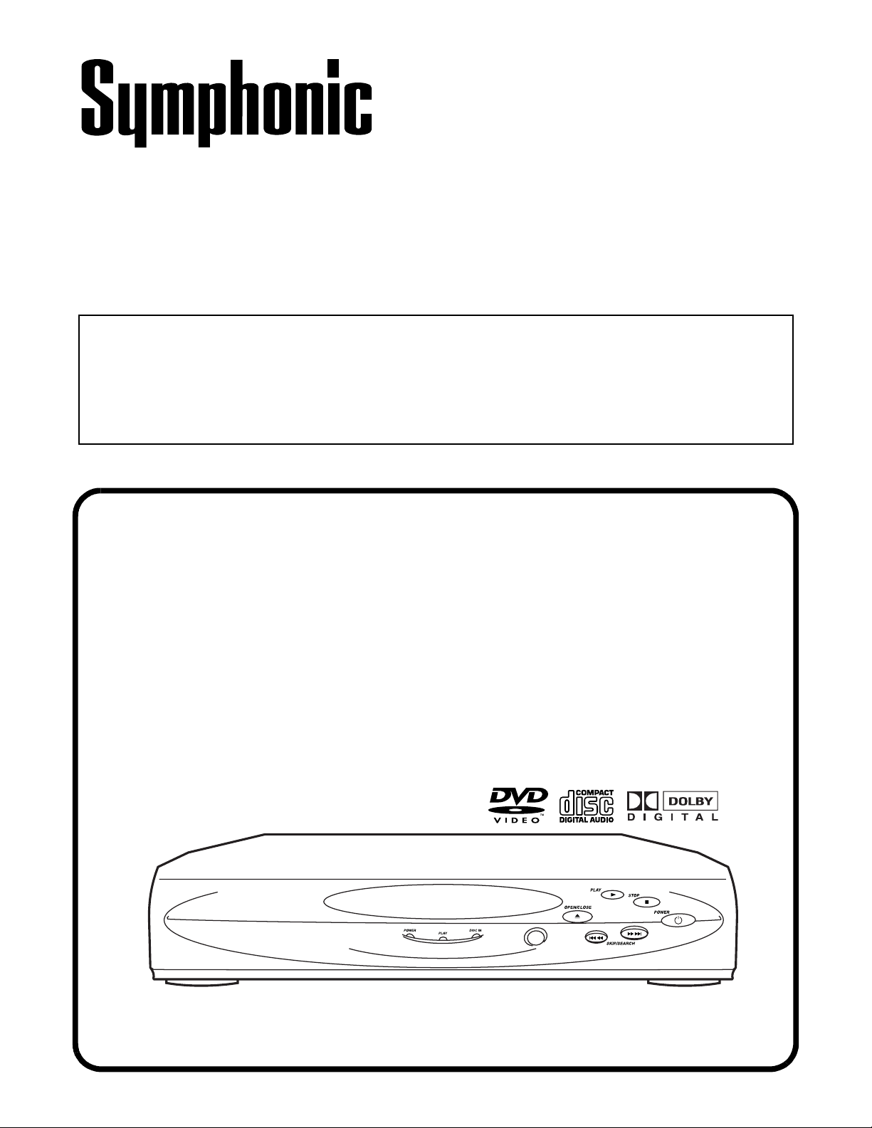
Page 1
SERVICE MANUAL
This service manual supplement (SD300D) contains only
the difference from the original model.
For all other data, see the original service manual for
DVL100D.
DVD PLAYER
SD300D
Page 2

IMPORTANT SAFETY NOTICE
Proper service and repair is important to the safe, reliable operation of all
Funai Equipment. The service procedures recommended by Funai and
described in this service manual are effective methods of performing
service operations. Some of these service special tools should be used
when and as recommended.
It is important to note that this service manual contains various CAUTIONS
and NOTICES which should be carefully read in order to minimize the risk of
personal injury to service personnel. The possibility exists that improper
service methods may damage the equipment. It also is important to
understand that these CAUTIONS and NOTICES ARE NOT EXHAUSTIVE.
Funai could not possibly know, evaluate and advice the service trade of all
conceivable ways in which service might be done or of the possible
hazardous consequences of each way. Consequently, Funai has not
undertaken any such broad evaluation. Accordingly, a servicer who uses a
service procedure or tool which is not recommended by Funai must first
use all precautions thoroughly so that neither his safety nor the safe
operation of the equipment will be jeopardized by the service method
selected.
TABLE OF CONTENTS
OPERATING CONTROLS AND FUNCTIONS . . . . . . . . . . . . . . . . . . . . . . . . . . . . . . . . . . . . . . . . . . . . . . . . 1-1-1
CABINET DISASSEMBLY INSTRUCTIONS . . . . . . . . . . . . . . . . . . . . . . . . . . . . . . . . . . . . . . . . . . . . . . . . . . 1-2-1
BLOCK DIAGRAMS. . . . . . . . . . . . . . . . . . . . . . . . . . . . . . . . . . . . . . . . . . . . . . . . . . . . . . . . . . . . . . . . . . . . . 1-3-1
SCHEMATIC DIAGRAMS / CBA’S AND TEST POINTS . . . . . . . . . . . . . . . . . . . . . . . . . . . . . . . . . . . . . . . . . 1-4-1
LEAD IDENTIFICATIONS . . . . . . . . . . . . . . . . . . . . . . . . . . . . . . . . . . . . . . . . . . . . . . . . . . . . . . . . . . . . . . . . 1-5-1
EXPLODED VIEWS . . . . . . . . . . . . . . . . . . . . . . . . . . . . . . . . . . . . . . . . . . . . . . . . . . . . . . . . . . . . . . . . . . . . . 1-6-1
DIFFERENT PARTS FROM ORIGINAL MODEL (DVL100) . . . . . . . . . . . . . . . . . . . . . . . . . . . . . . . . . . . . . . 1-7-1
Manufactured under license from Dolby Laboratories. "Dolby"
and the double-D symbol are trademarks of Dolby Laboratories.
Page 3
y
g
h
h
KLL
g
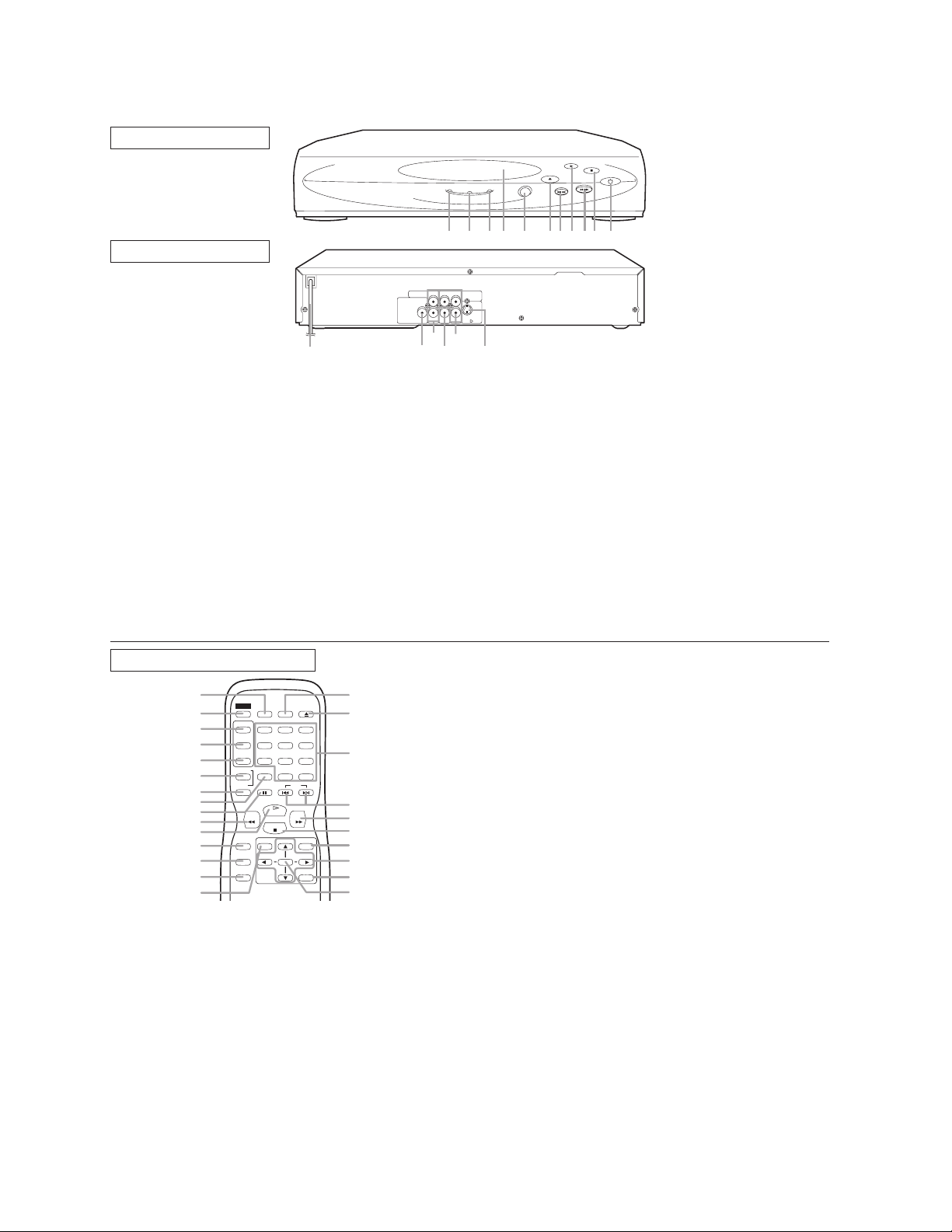
OPERATING CONTROLS AND FUNCTIONS
FRONT PANEL
POWER D ISC IN
PLAY
OPEN/CLOSE
PLAY
STOP
POWER
SKIP/SEARCH
REAR VIEW
1. POWER
to switch the player to ON or OFF
2. STOP
to stop playback
3. SKIP G / SEARCH
goes to next chapter or track during playback; press and
hold for 1.5 seconds for a forward search
4. PLAY
to start or resume disc playback
5. SKIP H / SEARCH
goes to previous chapter or track during playback; press
and hold for 1.5 seconds for a reverse search
6. OPEN/CLOSE
to open/close the disc tray
7. Remote Sensor window
8. Disc tray
9. DISC IN indicator
light appears when a disc is in the DVD player
10. PLAY indicator
y
REMOTE CONTROL
1
2
3
4
5
6
7
8
9
10
11
12
13
14
15
1. DISPLAY
to access or remove the display screen during DVD or
Audio CD playback
2. POWER
switch DVD player ON or OFF
3. AUDIO
to choose audio languages or sound modes
4. SUBTITLE
subtitle language DVD selector
5. ANGLE
select DVD camera angle
6. REPEAT
repeat chapter, track, title, all.
7. REPEAT A-B
repeat a specific segment
8. CLEAR
to reset the setting
9. PAUSE
pause playback temporarily / frame-by-frame playback
POWER
AUDIO
TITLE
ANGLE
REPEAT
SETUP
MODE
ZOOM
DISPLAY
SUB
CLEAR
TITLE
12
g
h
OPEN/
SEARCH
CLOSE
MODE
123
456
789
0 +10
SKIPPAUSEA-B
PLAY
FWDREV
STOP
MENU
ENTER
RETURN
[Fig. 1]
[Fig. 2]
AUDIO OUT
DIGITAL AUDIO OUT
PCM / BITSTREAM
VIDEO
OUT
131415 17
YCr
16
16 357891011 4 2
COMPONENT
VIDEO OUT
S-VIDEO OUT
CbLRCOAXIAL
11. POWER indicator
lights when the power is on
12. MAIN (AC Power Cord)
connect to a standard AC outlet
13. COAXIAL (Digital audio out)
connect to AUDIO inputs of a digital (coaxial) audio
equipment
14. AUDIO OUT (Left/Right)
connect to AUDIO inputs of an amplifier, receiver or
stereo system
15. VIDEO OUT
connect to the Video Input of a TV.
16. COMPONENT VIDEO OUT
connect to a TV with Component video in jacks.
17. S-VIDEO OUT
connect to a TV with S-Video inputs
Caution: Do not touch the inner pins of the jacks on the
rear panel. Electrostatic discharge may cause permanent
damage to the player.
10. REV
h
to view DVD picture in fast reverse motion
25
24
11. PLAY
to start a DVD disc playback
12. SETUP
to access or remove the DVD setup menu
13. MODE
23
to set up programmed or random playback (Audio CD)
to set the black level and virtual surround during DVD
playback
22
21
20
19
18
17
16
[Fig. 3]
14. ZOOM
enlarge DVD video image
15. TITLE
to display title menu of a disc
16. ENTER
acknowledge menu selection
17. RETURN
to return previous or remove setup menu
18. Arrow (sB
K
)
select an item in the menu
19. MENU
to display the menu of the DVD disc
20. STOP
to stop a DVD disc playback
21. FWD
g
to view DVD picture in fast forward motion
22. SKIP H,G
to skip chapter/tracks
23. 0-9 Number buttons
select numbered items in a menu
+10
use this button to enter number 10 and above
24. OPEN/CLOSE
to open/close the disc tray
25. SEARCH MODE
to locate a desired point
1-1-1 E5760IB
Page 4
CABINET DISASSEMBLY INSTRUCTIONS
1. Disassembly Flowchart
This flowchart indicates the disassembly steps to gain
access to item(s) to be serviced. When reassembling,
follow the steps in reverse order. Bend, route, and
dress the cables as they were originally.
[1] Top Cover
[2] Front Assembly
[3] DVD Mecha
[5] DVD Main CBA Unit[4] AV CBA
[7] Main CBA Holder[6] Rear Panel
2. Disassembly Method
REMOVAL
ID/
LOC.
No.
[1] Top Cover D1 5(S-1) -
[2]
[3]
[4] AV CBA D5
[5]
[6]
[7]
PART
Front
Assembly
DVD
Mecha
DVD Main
CBA Unit
Rear
Panel
Main CBA
Holder
REMOVE/*UNHOOK/
Fig.
UNLOCK/RELEASE/
No.
UNPLUG/DESOLDER
*2(L-1), Tray Panel,
D2
*2(L-2), *5(L-3)
D3,D43(S-2), *CN201,
*CN301
4(S-3), 3(S-4),
*CN1001, *CN1601
D5 2(S-5) -
D6 3(S-6) -
D6 (S-7) -
Note
1-1
1-2
1-3
1-4
1-5
1-6
2
2-1
2-2
2-3
3
-
(1): Identification (location) No. of parts in the figures
(2): Name of the part
(3): Figure Number for reference
(4): Identification of parts to be removed, unhooked,
unlocked, released, unplugged, unclamped, or
desoldered.
P=Spring, L=Locking Tab, S=Screw,
CN=Connector
*=Unhook, Unlock, Release, Unplug, or Desolder
e.g. 2(S-2) = two Screws (S-2),
2(L-2) = two Locking Tabs (L-2)
(5): Refer to “Reference Notes.”
Reference Notes
CAUTION 1: Locking Tabs (L-1), (L-2) and (L-3) are
fragile. Be careful not to break them.
1-1. Connect the wall plug to an AC outlet and press
the OPEN/CLOSE button to open the Tray.
1-2. Remove the Tray Panel by releasing two Locking
Tabs (L-1).
1-3. Press the OPEN/CLOSE button again to close
the Tray.
1-4. Press the POWER button to turn the power off.
1-5. Unplug an AC cord.
1-6. Release two Locking Tabs (L-2). Then, release
five Locking Tabs (L-3) (to do this, first release
two Locking Tabs (A) at the side, and then three
Locking Tabs (B) at the bottom.)
CAUTION 2: Electrostatic breakdown of the laser
diode in the optical system block may occur as a
potential difference caused by electrostatic charge
accumulated on cloth, human body etc, during
unpacking or repair work.
To avoid damage of pickup follow next procedures.
2-1. Slide out the pickup unit as shown in Fig. D4.
2-2. Short the three short lands of FPC cable with sol-
der before removing the FFC cable (CN201) from
it. If you disconnect the FFC cable (CN201), the
laser diode of pickup will be destroyed. (Fig. D4)
2-3. Disconnect Connector (CN301). Remove three
Screws (S-2) and lift the DVD Mecha. (Fig. D3)
CAUTION 3: When reassembling, confirm the FFC
cable (CN201) is connected completely. Then remove
the solder from the three short lands of FPC cable.
(Fig. D4)
↓
(1)
↓
(2)
↓
(3)
↓
(4)
↓
(5)
1-2-1 E5760DC
Page 5
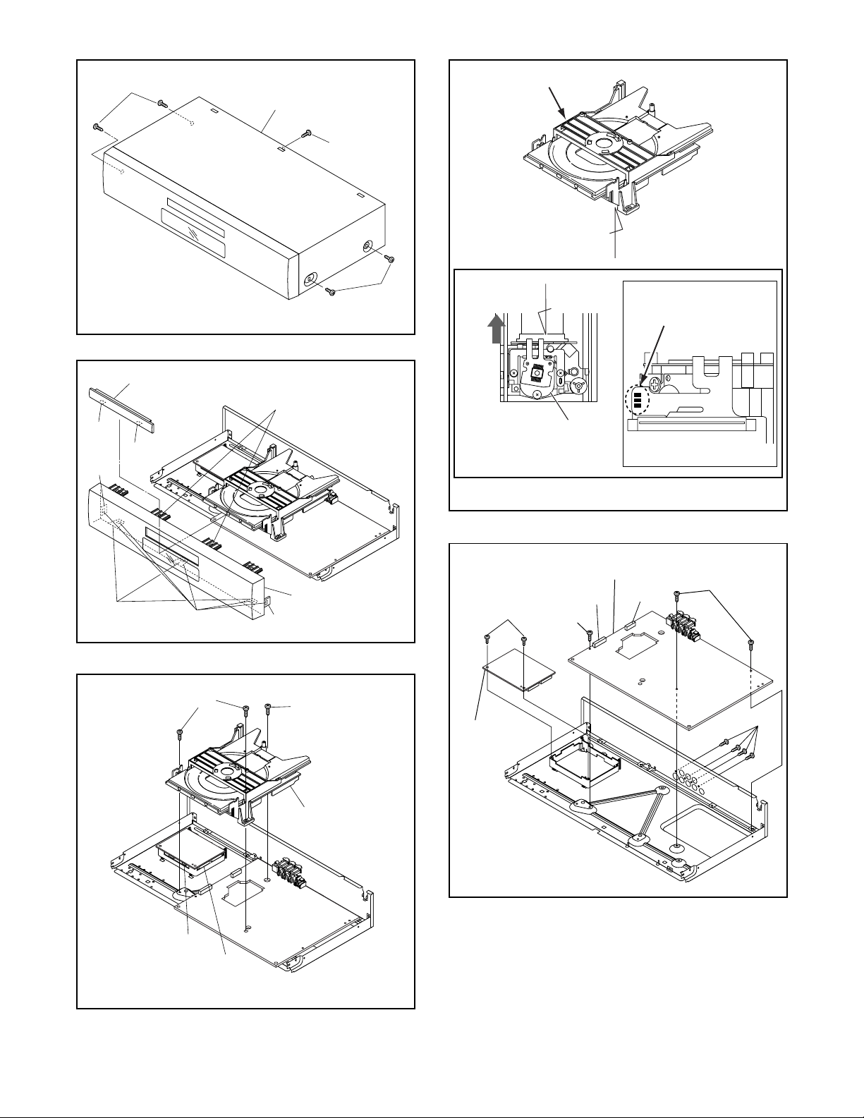
)
(S-1)
4
DVD Mecha
[1] Top Cover
(S-1)
A
(L-1)
(A)
(B)
Tray Panel
(L-1)
(L-3)
(L-2)
[2] Front Assembly
(A)
(S-1
Fig. D1
Fig. D2
Slide
B
Pickup Unit
View for A
(S-5)
[4] AV CBA
CN1001
(S-4)
Short the three short
lands by soldering
View for B
CN1601
Fig. D
(S-4)
(S-2)
CN301
CN201
(S-2)
[3] DVD Mecha
Fig. D3
[5] DVD Main
CBA Unit
(S-3)
Fig. D5
1-2-2 E5760DC
Page 6
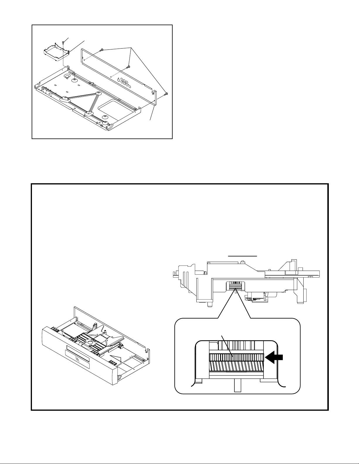
(S-8)
[7] Holder
(S-7)
[6] Rear Panel
Fig. D6
HOW TO MANUAL EJECT
1. Remove the Top Case.
2. Rotate the roulette in the direction of the arrow as
shown below.
View for A
Rotate this roulette in
the direction of the arrow
A
1-2-3 E5760DC
Page 7
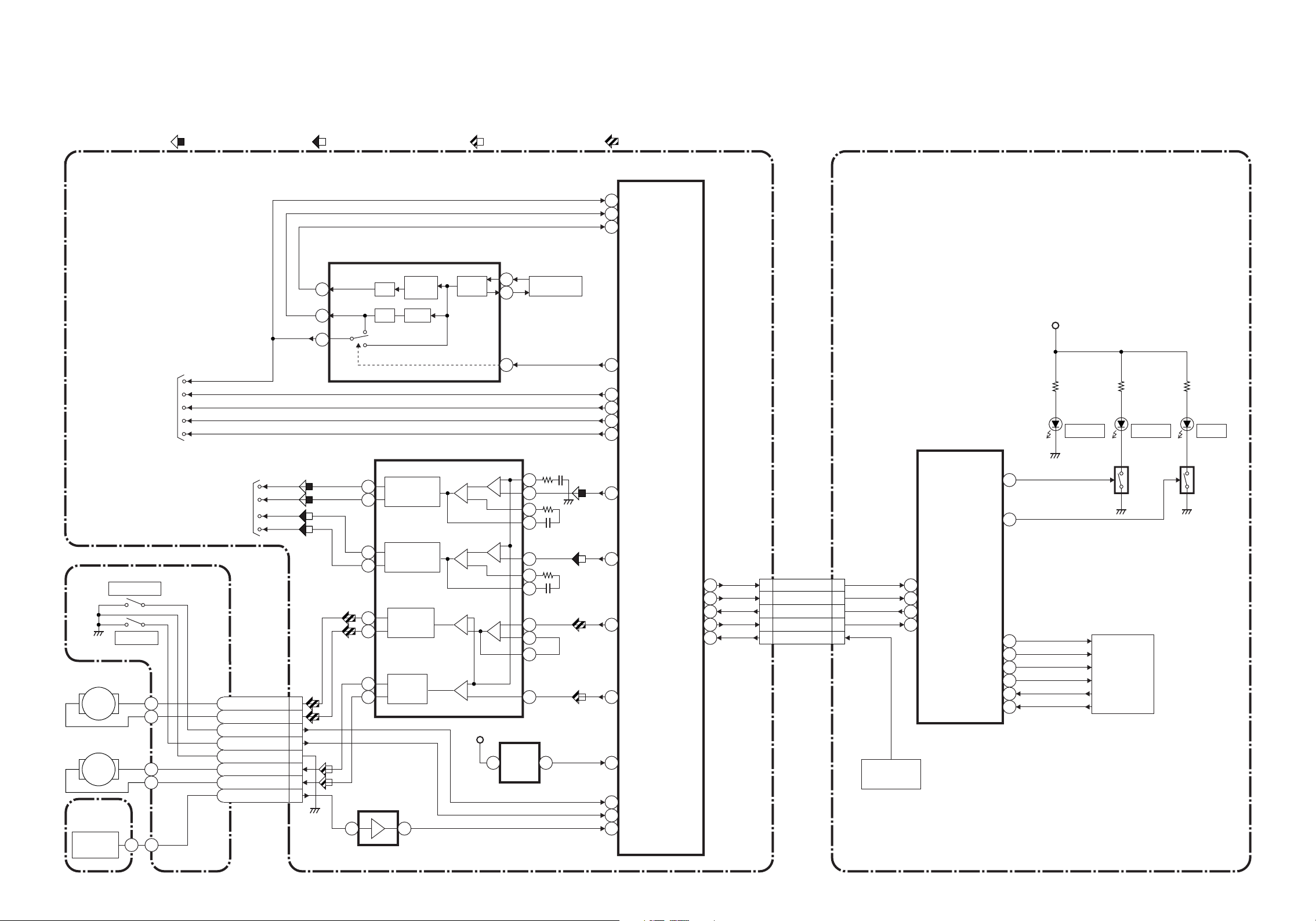
System Control/Servo Block Diagram
BLOCK DIAGRAMS
TO VIDEO/ AUDIO
BLOCK DIAGRAM
FOCUS SERVO SIGNAL TRACKING SERVO SIGNAL
IC451
(CLOCK GENERATOR)
3
15
10
PCM-SCLK
A-MUTE
ADAC-MD
ADAC-MC
ADAC-ML
MULTI
1/4
PLL
1/4
PLL2
IC301
(SERVO DRIVE)
SLED SERVO SIGNAL SPINDLE SERVO SIGNAL
IC101
(MICRO CONTROLLER)
EXT CLOCK
172
CLK33M
BE CLOCK
170
X451
X'TAL
OSC
7
8
14
36.864MHz
OSC
1792FSEL
95
A-MUTE
ADAC-MD
51
50 ADAC-MC
96 ADAC-ML
IC2001
(FRONT PANEL CONTROL)
+5V
D2003
POWER
D2001
DISC IN
D2002
PLAY
SPINDLE
MOTOR
M
SLED
MOTOR
M
FG CBA
FG
SENSOR
TRAY-OUT
TRAY-IN
TO DIGITAL SIGNAL
PROCESS BLOCK
DIAGRAM
DRIVE CBA
FS(+)
FS(-)
TS(+)
TS(-)
CN301
3SP(+)
4SP(-)
5TRAY-OUT
6TRAY-IN
7GND
8SL(-)
9SL(+)
1FG-IN
FOCUS
15
ACTUATOR
DRIVE
16
TRACKING
14
ACTUATOR
DRIVE
13
SPINDLE
12
MOTOR
DRIVE
11
SLED
17
MOTOR
DRIVE
18
IC202
(OP AMP)
12 14
KEY-1
KEY-2
KEY-3
KEY-4
K2
K1
18DISC IN LED
17
7
8
9
10
4
3
-
+
-
+
-
+
-
+3.3V
27
+
-+
26
25
24
+
-
1
2
3
4
+
-
5
6
23
IC461
RESET
5 4
152
FOCUS DRIVE
TRACKING
150
DRIVE
SPDL71
SLD70
RESET68
TRAY-OUT
97
TRAY-IN
60
FG-IN
66
FP-STB
FP-DOUT
FP-CLK
REMOTE
59
54FP-DIN
55
53
61
CN401 CN1001
FP-STB 16
16
FP-DIN 18
18
FP-DOUT 20
20
FP-CLK 21
21
REMOTE 22
22
RM2001
REMOTE
SENSOR
2
FP-STB
28
FP-DIN
27
FP-DOUT
1
FP-CLK
PLAY LED
DVD MAIN CBA UNIT AV CBA
KEY
MATRIX
Q2001
Q2003
1-3-1
1-3-2
E5760BLS
Page 8

SCHEMATIC DIAGRAMS / CBA’S AND TEST POINTS
Standard Notes
WARNING
Many electrical and mechanical parts in this chassis
have special characteristics. These characteristics
often pass unnoticed and the protection afforded by
them cannot necessarily be obtained by using replacement components rated for higher voltage, wattage,
etc. Replacement parts that have these special safety
characteristics are identified in this manual and its
supplements; electrical components having such features are identified by the mark " # " in the schematic
diagram and the parts list. Before replacing any of
these components, read the parts list in this manual
carefully. The use of substitute replacement parts that
do not have the same safety characteristics as specified in the parts list may create shock, fire, or other
hazards.
Notes:
1. Do not use the part number shown on these drawings for ordering. The correct part number is
shown in the parts list, and may be slightly different
or amended since these drawings were prepared.
2. All resistance values are indicated in ohms
3
(K=10
3. Resistor wattages are 1/4W or 1/6W unless otherwise specified.
4. All capacitance values are indicated in µF
(P=10
5. All voltages are DC voltages unless otherwise
specified.
, M=106).
-6
µF).
1-4-1 SC_FN1
Page 9

LIST OF CAUTION, NOTES, AND SYMBOLS USED IN THE SCHEMATIC DIAGRAMS ON THE FOLLOWING
PAG ES :
1. CAUTION:
FOR CONTINUED PROTECTION AGAINST FIRE HAZARD, REPLACE ONLY WITH THE
SAME TYPE FUSE.
F
A V
ATTENTION: POUR UNE PROTECTION CONTINUE LES RISQES D'INCELE N'UTILISER QUE
DES FUSIBLE DE MÊME TYPE.
RISK OF FIRE-REPLACE FUSE AS MARKED.
This symbol means fast operating fuse.
Ce symbole represente un fusible a fusion rapide.
2. CAUTION:
Fixed Voltage (or Auto voltage selectable) power supply circuit is used in this unit.
If Main Fuse (F1001) is blown, first check to see that all components in the power supply circuit are not defective
before you connect the AC plug to the AC power supply. Otherwise it may cause some components in the
power supply circuit to fail.
3. Note:
(1) Do not use the part number shown on the drawings for ordering. The correct part number is shown in the parts
list, and may be slightly different or amended since the drawings were prepared.
(2) To maintain original function and reliability of repaired units, use only original replacement parts which are
listed with their part numbers in the parts list section of the service manual.
4. Wire Connectors
(1) Prefix symbol "CN" means "connector" (can disconnect and reconnect).
(2) Prefix symbol "CL" means "wire-solder holes of the PCB" (wire is soldered directly).
5. Voltage indications for PLAY and STOP mode on the schematics are as shown below:
5.0
2
3
5.0
(2.5)
Indicates that the voltage
is not consistent here.
PLAY mode
STOP mode
1
(Unit: Volt)
The same voltage for
both PLAY & STOP modes
6. How to read converged lines
1-D3
Distinction Area
3
AREA D3
Line Number
(1 to 3 digits)
2
AREA B1
Examples:
1. "1-D3" means that line number "1" goes to area "D3".
1
1-D3
2. "1-B1" means that line number "1" goes to area "B1".
ABCD
7. Test Point Information
: Indicates a test point with a jumper wire across a hole in the PCB.
: Used to indicate a test point with a component lead on foil side.
1-B1
: Used to indicate a test point with no test pin.
: Used to indicate a test point with a test pin.
1-4-2 SC_FN2
Page 10

AV 1/3 Schematic Diagram
AV 1/3
Ref No. Position
IC1001 B-1
IC1002 D-4
IC1006 C-1
Q1001 B-3
Q1002 D-3
Q1003 B-2
Q1004 D-3
Q1005 D-2
Q1006 D-1
Q1011 D-1
Q1015 D-2
Q1016 E-2
CN1001 F-4
ICS
TRANSISTORS
CONNECTOR
CAUTION !
Fixed voltage ( or Auto voltage selectable ) power supply circuit is used in this unit.
If Main Fuse (F001) is blown, check to see that all components in the power supply
circuit are not defective before you connect the AC plug to the AC power supply.
Otherwise it may cause some components in the power supply circuit to fail.
F
A V
CAUTION
FOR CONTINUED PROTECTION AGAINST FIRE HAZARD,
REPLACE ONLY WITH THE SAME TYPE FUSE.
ATTENTION : POUR UNE PROTECTION CONTINUE LES RISQES
D'INCELE N'UTILISER QUE DES FUSIBLE DE MÊME TYPE.
RISK OF FIRE-REPLACE FUSE AS MARKED.
"This symbol means fast operating fuse."
"Ce symbole reprèsente un fusible à fusion rapide."
NOTE :
The voltage for parts in hot circuit is measured
using hot GND as a common terminal.
A4
A3
B4
B3
C4
C3
D4
D3
E4
E3
F4
F3
A2
A1
B2
B1
1-4-3 1-4-4
C2
C1
D2
D1
E2
E1
F2
F1
E5760SCAV1
Page 11

AV 2/3 Schematic Diagram
AV 2/3
Ref No. Position
IC1201 H-1
IC1402 I-3
Q1201 J-1
Q1202 J-1
Q1203 I-2
Q1204 I-1
Q1351 J-4
Q1352 H-2
CN1601 G-3
ICS
TRANSISTORS
CONNECTOR
VIDEO SIGNAL
DATA(AUDIO)
AUDIO SIGNAL
G4
G3
H4
H3
I4
I3
J4
J3
K4
K3
L4
L3
G2
G1
1-4-5
H2
H1
I2
I1
J2
J1
K2
K1
1-4-6
L2
L1
E5760SCAV2
Page 12

AV 3/3 Schematic Diagram
AV 3/3
Ref No. Posit ion
IC2001 O-3
Q2001 O-3
Q2003 P-3
IC
TRANSISTORS
M4
M3
N4
N3
O4
O3
P4
P3
Q4
Q3
M2
M1
N2
N1
O2
O1
P2
P1
Q2
Q1
1-4-7 1-4-8
E5760SCAV3
Page 13

AV CBA Top View
CAUTION !
Fixed voltage ( or Auto voltage selectable ) power supply circuit is used in this unit.
If Main Fuse (F001) is blown, check to see that all components in the power supply
circuit are not defective before you connect the AC plug to the AC power supply.
Otherwise it may cause some components in the power supply circuit to fail.
CAUTION
F
A V
FOR CONTINUED PROTECTION AGAINST FIRE HAZARD,
REPLACE ONLY WITH THE SAME TYPE FUSE.
ATTENTION : POUR UNE PROTECTION CONTINUE LES RISQES
D'INCELE N'UTILISER QUE DES FUSIBLE DE MÊME TYPE.
RISK OF FIRE-REPLACE FUSE AS MARKED.
"This symbol means fast operating fuse."
"Ce symbole reprèsente un fusible à fusion rapide."
NOTE :
The voltage for parts in hot circuit is measured
using hot GND as a common terminal.
1-4-9
1-4-10
BE5701F01014A
Page 14

AV CBA Bottom View
AV CBA
Ref No. Position
IC1001 C-2
IC1002 B-2
IC1006 C-2
IC1201 D-3
IC1402 E-5
IC2001 A-4
Q1001 C-1
Q1002 B-2
Q1003 D-1
Q1004 B-2
Q1011 A-1
Q1016 B-1
Q1201 E-3
Q1202 E-3
Q1203 E-3
Q1204 E-3
Q1351 E-2
Q1352 D-2
Q2001 A-3
Q2003 A-4
CN1001 B-5
CN1601 D-5
ICS
TRANSISTORS
CONNECTORS
WF1
PIN 5 OF
CN1601
WF2
PIN 7 OF
CN1601
WF3
PIN 21 OF
IC1402
WF4
PIN 11 OF
CN1601
WF5
PIN 13 OF
CN1601
WF6
PIN 16 OF
CN1601
CAUTION !
Fixed voltage ( or Auto voltage selectable ) power supply circuit is used in this unit.
If Main Fuse (F001) is blown, check to see that all components in the power supply
circuit are not defective before you connect the AC plug to the AC power supply.
Otherwise it may cause some components in the power supply circuit to fail.
CAUTION
F
A V
FOR CONTINUED PROTECTION AGAINST FIRE HAZARD,
REPLACE ONLY WITH THE SAME TYPE FUSE.
ATTENTION : POUR UNE PROTECTION CONTINUE LES RISQES
D'INCELE N'UTILISER QUE DES FUSIBLE DE MÊME TYPE.
RISK OF FIRE-REPLACE FUSE AS MARKED.
"This symbol means fast operating fuse."
"Ce symbole reprèsente un fusible à fusion rapide."
NOTE :
The voltage for parts in hot circuit is measured
using hot GND as a common terminal.
1-4-11
1-4-12
BE5701F01014A
Page 15

E C B
2SA1015-Y (TPE2)
KTA1266 (Y)
KTC3198 (Y)
2SC2120-Y(TPE2)
KTC3203(Y)
LEAD IDENTIFICATIONS
2SK3374
2SC2785 (H)
KTC3199 (GR)
KTA1267 (Y)
KRC101M
BA1L3M-T
S D G
E C B
NJM4558D
KIA4558P
8 5
1 4
PQ070XF01SZ
MM1622XJBE
24
1
13
12
PT6313-S-TP
28
1
LTV-817(B,C)-F
KIA431-AT
15
14
K A R
1234
1: Vin
2: Vo
3: GND
4: Vc
A
K
C
E
Note:
A: Anode
K: Cathode
E: Emitter
C: Collector
B: Base
R: Reference
G: Gate
D: Drain
S: Source
1-5-1 E5760LE
Page 16

Cabinet
See Electrical Parts List
for parts with this mark.
Some Ref. Numbers are
not in sequence.
2L105
2L101
EXPLODED VIEWS
2L011
2L011
A16
2L021
A2
2L021
2L021
2L011
1B1
DVD Main
CBA Unit
2B3
W1001
2L031
W1601
AV CBA
A17
JK1401
2L031
2L071
JK1404
JK1202
2L031
2L071
F1001
AC1001
2L041
A21
A22
2L071
A1X
A23
A13
A15
A13
1-6-1 E5760EX
Page 17

DIFFERENT PARTS FROM ORIGINAL MODEL (DVL100)
PRODUCT SAFETY NOTE: Products marked with a
# have special characteristics important to safety.
Before replacing any of these components, read carefully the product safety notice in this service manual.
Don't degrade the safety of the product through
improper servicing.
NOTES:
1. Parts that are not as signed part numbers (---------)
are not available.
2. Tolerance of Capacitors and Resistors are noted
with the following symbols.
C.....±0.25% D.....±0.5% F.....±1%
G.....±2% J......±5% K.....±10%
M.....±20% N.....±30% Z.....+80/-20%
Ref. No. Description Part No.
Mechanical Parts
A1X FRONT ASSEMBLY E5760UD 0VM203943
A2 TRAY PANEL E5760UD 0VM203874
A15 MAIN CHASSIS E5760UD 0VM101209
A16 TOP COVER E5626UD 0VM305489
A17 REAR PANEL E5760UD 0VM203857
A21 LABEL, MODEL NO. E5760UD ---------A22 LABEL, BAR CODE E5760UD ---------A23 LABEL, TELEPHONE NUMBER
2B3 HOLDER, MAIN PCB E5700UD 0VM305832B
2B24 Not used
2L011 SCREW, C-TIGHT M3X5 BIND HEAD +GBKC3050
2L082 Not used
S1 GIF T BOX CARTON E5760UD 0VM306367
S2 STYROFOAM E5720UD 0VM101249
S4 UNIT, BAG V4010PA 0VM406453B
X1 REMOTE CONTROL UNIT DVD 0842
X10# OWNER'S MANUAL E5760UD 0VMN03738
X36 RETURN STOP SHEET HD400UD 0VM414373
Electrical Parts
C1001# MET ALLIZED FILM CAP . 0.01µ F/ 275V
# METALLIZED FILM CAP . 0.01µF /250V
# METALLIZED FILM CAP . 0.01µF /250V KCT2E103DC011
C1003 ELECTROLYTIC CAP. 2.2µF /250V M orCA2E2R2S6009
C1004 ELECTROLYTIC CAP. 82µF/200V M orCA2D820S6014
H5720UD
VCDVR040 or
REMOTE CONTROL UNIT DVD 0842
VCDVR040
DVD MAIN CBA UNIT N79F1GUP
AV CBA 0VSA14300
K or
M or
ELECTROLYTIC CAP. 2.2µF/250V
M(105°C)
ELECTROLYTIC CAP. 82µF/200V M CA2D820NC002
----------
NA603UD
NA653UD
CT2E103HJE05
CT2E103MS037
CE2EMASTH2R2
Ref. No. Description Part No.
C1005 CERAMIC CAP. CH J 56pF/500V CCD2JJPCH560
C1006# SAFETY CAP. 2200pF/250V or CCD2EMA0E222
# SAFETY CAP. 2200pF/250V or CCG2EMA0F222
# SAFETY CAP. 2200pF/125V CCG2BMA0E222
C1007 ELECTROLYTIC CAP. 1000µF/6.3V M CE0KMASDL102
C1009 ELECTROLYTIC CAP. 2200µF/6.3V M CE0KMASTL222
C1010 CERAMI C CAP.(AX) CH J 560pF/50V CA1J561TU008
C1013 FILM CAP.(P) 0.0033µF/50V J or CMA1JJS 00332
FILM CAP.(P) 0.0033µF/50V J CA1J332MS029
C1014 ELECTOLYTIC CAP. 1000µF/6. 3V
C1017 CERAMI C CAP.(AX) Y M 0.01µF/16V CCA1CMT0Y103
C1018 ELECTROLYTIC CAP. 100µF/6.3V M CE0KMASDL101
C1021 CHIP CERAMIC CAP. B K 0.01µF/50V CHD1JK30B103
C1022 CHIP CERAMIC CAP. B K 0.01µF/50V CHD1JK30B103
C1029 CERAMI C CAP.(AX) X K 2200pF/16V CCA1CKT0X222
C1034 ELECTROLYTIC CAP. 100µF/6.3V M CE0KMASDL101
C1035 ELEC TROLYTIC CAP. 470µF/16V M CE1CMASDL471
C1036 CHIP CERAMIC CAP. B K 0.01µF/50V CHD1JK30B103
C1037 CHIP CERAMIC CAP. F Z 0.1µF/50V CHD1JZ30F 104
C1038 ELECTROLYTIC CAP. 470µF/6.3V M CE0KMASDL471
C1039 CHIP CERAMIC CAP. F Z 0.1µF/50V CHD1JZ30F 104
C1047 FILM CAP.(P) 0.01µF/50V J or CMA1JJS00103
C1048 ELEC TROLYTIC CAP. 220µF/16V M CE1CMASDL221
C1201 ELEC TROLYTIC CAP. 10µF/16V M CE1CMASDL100
C1202 ELEC TROLYTIC CAP. 10µF/16V M CE1CMASDL100
C1205 CHIP CERAMIC CAP. CH J 220pF/
C1206 CHIP CERAMIC CAP. CH J 220pF/
C1207 CHIP CERAMIC CAP. CH J 47pF/50V CHD1JJ3CH470
C1208 CHIP CERAMIC CAP. CH J 47pF/50V CHD1JJ3CH470
C1221 ELEC TROLYTIC CAP. 10µF/16V M CE1CMASDL100
C1222 ELEC TROLYTIC CAP. 10µF/16V M CE1CMASDL100
C1223 CHIP CERAMIC CAP. CH J 1000pF/
C1224 CHIP CERAMIC CAP. CH J 1000pF/
C1245 CHIP CERAMIC CAP. F Z 0.1µF/50V CHD1JZ30F 104
C1246 CHIP CERAMIC CAP. F Z 0.1µF/50V CHD1JZ30F 104
C1247 ELECTROLYTIC CAP. 470µF/6.3V M CE0KMASDL471
C1249 ELEC TROLYTIC CAP. 47µF/16V M CE1CMASDL470
C1351 CHIP CERAMIC CAP. B K 0.1µF/25V CHD1EK30B104
C1352 ELECTROLYTIC CAP. 47µF/6.3V M CE0KMASDL470
C1354 CHIP CERAMIC CAP. CH J 100pF/
C1358 CHIP CERAMIC CAP. CH D 9pF/50V CHD1JD3CH9R0
C1394 ELECTROLYTIC CAP. 47µF/6.3V M CE0KMASDL470
C1395 ELECTROLYTIC CAP. 470µF/6.3V M CE0KMASDL471
C1402 ELECTROLYTIC CAP. 470µF/6.3V M CE0KMASDL471
C1421 CHIP CERAMIC CAP. B K 0.01µF/50V CHD1JK30B103
C1422 CHIP CERAMIC CAP. B K 0.1µF/25V CHD1EK30B104
C1441 CHIP CERAMIC CAP. B K 0.33µF/10V CHD1AK30B334
C1442 ELECTROLYTIC CAP. 470µF/6.3V M CE0KMASDL471
M(105°C) or
ELECTOLYTIC CAP. 1000µF /6.3V
M(105°C)
FILM CAP.(P) 0.01µF/50V J CA1J103MS029
50V
50V
50V
50V
50V
CA0K102S6026
CE0KMASDH102
CHD1JJ3CH221
CHD1JJ3CH221
CHD1JJ3CH102
CHD1JJ3CH102
CHD1JJ3CH101
1-7-1 E5760PL
Page 18

Ref. No. Description Part No.
C1461 ELECTROLYTIC CAP. 1µF/50V M CE1JMASDL010
C1462 ELECTROLYTIC CAP. 470µF/6.3V M CE0KMASDL471
C1481 ELECTROLYTIC CAP. 1µF/50V M CE1JMASDL010
C1482 ELECTROLYTIC CAP. 470µF/6.3V M CE0KMASDL471
C1522 ELECTROLYTIC CAP. 10µF/16V M CE1CMASDL100
C1524 ELECTROLYTIC CAP. 100µF/6.3V M CE0KMASDL101
C1531 CHIP CERAMIC CAP. B K 0.01µF/50V CHD1JK30B103
C1532 ELECTROLYTIC CAP. 22µF/6.3V M CE0KMASDL220
C1533 CHIP CERAMIC CAP. F Z 0.1µF/50V CHD1JZ30F104
C2004 CHIP CERAMIC CAP. F Z 0.1µF/50V CHD1JZ30F104
C2011 CHIP CERAMIC CAP. F Z 0.1µF/50V CHD1JZ30F104
C2012 ELECTROLYTIC CAP. 100µF/6.3V M CE0KMASDL101
C2013 CHIP CERAMIC CAP. CH J 1000pF/
CN1001 22P FFC AV PCB TO MAIN WX1E5700-007
CN1601 16P FFC WX1E5700-008
D1001 RECTIFIER DIODE 1N4005 NDQZ001N4005
D1002 RECTIFIER DIODE 1N4005 NDQZ001N4005
D1004 RECTIFIER DIODE 1N4005 NDQZ001N4005
D1005 RECTIFIER DIODE 1N4005 NDQZ001N4005
D1006 SCHOTTKY BARRIER DIODE SB140 orNDQZ000SB140
D1008 SCHOTTKY BARRIER DIODE SB140 orNDQZ000SB140
D1011 RECTIFIER DIODE BA157 or NDQZ000BA157
D1012 SWITCHING DIODE 1N4148M or NDTZ01N4148M
D1016 RECTIFIER DIODE BA157 or NDQZ000BA157
D1018 SWITCHING DIODE 1N4148M or NDTZ01N4148M
D1024 SWITCHING DIODE 1N4148M or NDTZ01N4148M
D1030 RECTIFIER DIODE FR202 or NDQZ000FR202
D1046 ZENER DIODE DZ-5.6BSCT265 or NDTC0DZ5R6BS
D1047 ZENER DIODE DZ-5.1BSBT 265 or NDTB0DZ5R1BS
D1048 ZENER DIODE DZ-15BSAT265 or NDTA00DZ15BS
D1051 ZENER DIODE DZ-6.2BSBT 265 or NDTB0DZ6R2BS
D1053 PCB JUMPER D0.6-P10.0 JW10.0T
D1054 PCB JUMPER D0.6-P10.0 JW10.0T
D1058 SCHOTTKY BARRIER DIODE SB140 orNDQZ000SB140
D1301 ZENER DIODE DZ-5.6BSBT 265 or NDTB0DZ5R6BS
D2001 LED(GREEN) 204-10GD/S957 NPQZ10GDS957
D2002 LED(GREEN) 204-10GD/S957 NPQZ10GDS957
D2003 LED(RED) 204HD/E NPQZ00204HDE
50V
SCHOTTKY BARRIER DIODE
ERA81-004
SCHOTTKY BARRIER DIODE
ERA81-004
FAST RECOVERY DIODE ERA18-04 QD PZ 0ERA 1804
SWITCHING DIODE 1SS133(T-77) QDTZ001SS133
FAST RECOVERY DIODE ERA18-04 QD PZ 0ERA 1804
SWITCHING DIODE 1SS133(T-77) QDTZ001SS133
SWITCHING DIODE 1SS133(T-77) QDTZ001SS133
FAST RECOVERY DIODE ERB3201L3
ZENER DIODE MTZJT-775.6C QDTC0MTZJ5R6
ZENER DIODE MTZJT-775.1B QDTB0MTZJ5R1
ZENER DIODE MTZJT-7715A QDTA00MTZJ15
ZENER DIODE MTZJT-776.2B QDTB0MTZJ6R2
SCHOTTKY BARRIER DIODE
ERA81-004
ZENER DIODE MTZJT-775.6B QDTB0MTZJ5R6
CHD1JJ3CH102
QDPZERA81004
QDPZERA81004
QDQZ0ERB3201
QDPZERA81004
Ref. No. Description Part No.
D2005 SWITCHING DIODE 1N4148M or NDTZ01N4148M
SWITCHING DIODE 1SS133(T-77) QDTZ001SS133
D2006 SWITCHING DIODE 1N4148M or NDTZ01N4148M
SWITCHING DIODE 1SS133(T-77) QDTZ001SS133
D2007 SWITCHING DIODE 1N4148M or NDTZ01N4148M
SWITCHING DIODE 1SS133(T-77) QDTZ001SS133
D2008 SWITCHING DIODE 1N4148M or NDTZ01N4148M
SWITCHING DIODE 1SS133(T-77) QDTZ001SS133
D2010 PCB JUM PE R D0.6-P 5.0 JW5.0T
IC1001#PHOTOCOUPLER LTV-817B-F or NPEB0LTV817F
# PH OTOCOUP LER LTV-817C-F NPEC0LTV817F
IC1002 VOLTAG E REG ULATOR
IC1006 IC KIA431-AT NSZLA0TJY001
IC1201 IC:OP AMP KIA4558P or NSZBA0SJY004
IC1402 DRIVER FOR DVD MM1622XJB E QSZBA0TMM085
IC2001 FL DRIVER IC PT6313-S-TP NSZBA0TG2006
L1001# LINE FILTER 20MH SA-00911 LLBG00ZSA003
L1007 CHOKE COIL 22µH-K LLBD00PKV006
L1008 PCB JUMPER D0.6-P5.0 JW5.0T
L1009 CHOKE COIL 22µH-K LLBD00PKV006
L1011 BEAD CORE B16 RH 3.5X3X1.3 XL03003XM002
L1043 BEAD CORE B16 RH 4X3X2 XL03003XM001
L1060 BEAD CORE B16 RH 3.5X3X1.3 XL03003XM002
L1350 INDUCTOR 100µH-K-26T LLAXKATTU101
L1351 INDUCTOR 0.47µH-K-26T LLAXKATTUR47
L1401 CHIP INDUCTOR BK1608HM121-T LLBC003TU051
L1421 CHIP INDUCTOR BK1608HM121-T LLBC003TU051
L1441 CHIP INDUCTOR BK1608HM121-T LLBC003TU051
L1442 CHIP INDUCTOR BK1608HM121-T LLBC003TU051
L1461 CHIP INDUCTOR BK1608HM121-T LLBC003TU051
L1481 CHIP INDUCTOR BK1608HM121-T LLBC003TU051
L1521 CHOKE COIL 22µH-K LLBD00PKV006
L1522 CHIP BEAD MMZ1608R102CT XL06001TE002
L2001 PCB JUMPER D0.6-P5.0 JW5.0T
L2002 INDUCTOR 100µH-K-26T LLAXKATTU101
L2003 PCB JUMPER D0.6-P5.0 JW5.0T
Q1001# FET 2SK3374 QFWZ02SK3374
Q1002 TRANSISTOR KTA1267(Y) NQSY0KTA1267
Q1003 TRANSISTOR KTC3199(GR) or NQS10KTC3199
Q1004 TRANSISTOR KTC3198(Y) NQSY0KTC3198
Q1011 TRANSISTOR KTC3203(Y) or NQSY0KTC3203
Q1016 TRANSISTOR KTC3199(GR) or NQS10KTC3199
Q1201 TRANSISTOR KTC3199(GR) or NQS10KTC3199
Q1202 TRANSISTOR KTC3199(GR) or NQS10KTC3199
Q1203 TRANSISTOR KTA1266(Y) or NQSY0KT A1266
Q1204 TRANSISTOR KTA1266(Y) or NQSY0KT A1266
Q1351 TRANSISTOR KTC3199(GR) or NQS10KTC3199
PQ070XF01SZ
IC:OP AMP NJM4558D QSZBA0SJR006
TRANSISTOR 2SC2785(H) QQSH02SC2785
TRANSISTOR 2SC2120-Y(TPE2) QQSY02SC2120
TRANSISTOR 2SC2785(H) QQSH02SC2785
TRANSISTOR 2SC2785(H) QQSH02SC2785
TRANSISTOR 2SC2785(H) QQSH02SC2785
TRANSISTOR 2SA1015-Y(TPE2) QQSY02SA1015
TRANSISTOR 2SA1015-Y(TPE2) QQSY02SA1015
TRANSISTOR 2SC2785(H) QQSH02SC2785
QSZBA0SSH026
1-7-2 E5760PL
Page 19

Ref. No. Description Part No.
Q1352 TRANSISTOR KTC3199(GR) or NQS10KTC3199
TRANSISTOR 2SC2785(H) QQSH02SC2785
Q2001 RES. BUILT-IN TRANSISTOR
Q2003 RES. BUILT-IN TRANSISTOR
R1004 METAL OXIDE FILM RES. 2W J 82k Ω orRN02823ZU001
R1005 CARBON RES. 1/4W J 2.7M Ω RCX4JATZ0275
R1006 CARBON RES. 1/4W J 2.7M Ω RCX4JATZ0275
R1008 CARBON RES. 1/4W J 1k Ω RCX4JATZ0102
R1010 CARBON RES. 1/6W J 15k Ω or RCX6JATZ0153
R1011 METAL OXIDE FILM RES. 1W J 1.2 Ω orRN011R2ZU001
R1015 CARBON RES. 1/4W J 560 Ω RCX4JATZ0561
R1016 CARBON RES. 1/6W J 22k Ω or RCX6JATZ0223
R1017 CHIP RES.(1608) 1/10W J 5.6k Ω RRXAJR5Z0562
R1019 CHIP RES.(1608) 1/16W F 820 Ω or RRXGFR5Z 0821
R1020 CHIP RES.(1608) 1/10W J 2.7k Ω RRXAJR5Z0272
R1021 CHIP RES.(1608) 1/10W J 5.6k Ω RRXAJR5Z0562
R1022 CHIP RES.(1608) 1/10W J 820 Ω RRXAJR5Z0821
R1023 CHIP RES.(1608) 1/16W F 2.4k Ω or RRXGFR5Z0242
R1025 CHIP RES.(1608) 1/10W J 10k Ω RRXAJR5Z0103
R1029 CARBON RES. 1/6W J 470k Ω or RCX6JATZ0474
R1032 CARBON RES. 1/4W J 3.3k Ω RCX4JATZ0332
R1035 CARBON RES. 1/4W J 1k Ω RCX4JATZ0102
R1043 METAL OXIDE FILM RES. 1W J 2.7 Ω orRN012R7ZU001
R1044 CHIP RES.(1608) 1/10W J 100k Ω RRXAJR5Z0104
R1059 CHIP RES.(1608) 1/10W J 10k Ω RRXAJR5Z0103
R1067 CHIP RES.(1608) 1/10W J 1k Ω RRXAJR5Z0102
R1068 CARBON RES. 1/4W J 1k Ω RCX4JATZ0102
R1069 CARBON RES. 1/6W J 470 Ω or RCX6JATZ0471
R1073 METAL OXIDE FILM RES. 2W J 22 Ω orRN02220ZU001
R1074 RECTIFIER DIODE 1N4005 NDQZ001N4005
R1075 CHIP RES.(1608) 1/10W J 2.7k Ω RRXAJR5Z0272
R1076 CHIP RES.(1608) 1/10W J 10k Ω RRXAJR5Z0103
R1079 CARBON RES. 1/4W J 0.47 Ω RCX4JATZ0R47
R1080 CHIP RES.(1608) 1/10W J 22k Ω RRXAJR5Z0223
R1081 CHIP REG. 1/16W F 100 Ω or RRXGFR5Z0101
R1086 CHIP RES.(1608) 1/10W 0 Ω RRXAZR5Z0000
R1091 CHIP RES.(1608) 1/10W 0 Ω RRXAZR5Z0000
R1203 CHIP RES.(1608) 1/10W 0 Ω RRXAZR5Z0000
R1204 CHIP RES.(1608) 1/10W 0 Ω RRXAZR5Z0000
KRC101M or
RES. BUILT-IN TRANSISTOR
BA1L3M-T
KRC101M or
RES. BUILT-IN TRANSISTOR
BA1L3M-T
METAL OXIDE FILM RES. 2W J 82k Ω RN02823KE009
CARBON RES. 1/4W J 15k Ω RCX4JATZ0153
METAL OXIDE FILM RES. 1W J 1.2 Ω RN011R2KE009
CARBON RES. 1/4W J 22k Ω RCX4JATZ0223
CHIP RES. 1/10W F 820 Ω RRXAFR5Z8200
CHIP RES.(1608) 1/10W F 2.4k Ω RRXAFR5Z2401
CARBON RES. 1/4W J 470k Ω RCX4JATZ0474
METAL OXIDE FILM RES. 1W J 2.7 Ω RN012R7KE009
CARBON RES. 1/4W J 470 Ω RCX4JATZ0471
METAL OXIDE FILM RES. 2W J 22 Ω RN02220KE009
CHIP RES. 1/10W F 100 Ω RRXAFR5Z1000
NQSZ0KRC101M
QQSZ00BA1L3M
NQSZ0KRC101M
QQSZ00BA1L3M
Ref. No. Description Part No.
R1205 CHIP RES.(1608) 1/16W F 20k Ω or RRXGFR5Z0203
CHIP RES.(1608) 1/10W F 20k Ω RRXAFR5Z2002
R1206 CHIP RES.(1608) 1/16W F 20k Ω or RRXGFR5Z0203
CHIP RES.(1608) 1/10W F 20k Ω RRXAFR5Z2002
R1207 CHIP RES.(1608) 1/10W J 8.2k Ω RRXAJR5Z0822
R1208 CHIP RES.(1608) 1/10W J 8.2k Ω RRXAJR5Z0822
R1209 CHIP RES. 1/16W F 30k Ω or RRXGFR5Z0303
CHIP RES.(1608) 1/10W F 30k Ω RRXAFR5Z3002
R1210 CHIP RES. 1/16W F 30k Ω or RRXGFR5Z0303
CHIP RES.(1608) 1/10W F 30k Ω RRXAFR5Z3002
R1211 CHIP RES.(1608) 1/10W 0 Ω RRXAZR5Z0000
R1212 CHIP RES.(1608) 1/10W 0 Ω RRXAZR5Z0000
R1221 CHIP RES.(1608) 1/10W J 100k Ω RRXAJR5Z0104
R1222 CHIP RES.(1608) 1/10W J 100k Ω RRXAJR5Z0104
R1223 CHIP RES.(1608) 1/10W J 470 Ω RRXAJR5Z0471
R1224 CHIP RES.(1608) 1/10W J 470 Ω RRXAJR5Z0471
R1225 CHIP RES.(1608) 1/10W J 1k Ω RRXAJR5Z0102
R1226 CHIP RES.(1608) 1/10W J 1k Ω RRXAJR5Z0102
R1227 CHIP RES.(1608) 1/10W J 220 Ω RRXAJR5Z0221
R1228 CHIP RES.(1608) 1/10W J 220 Ω RRXAJR5Z0221
R1233 CHIP RES.(1608) 1/10W 0 Ω RRXAZR5Z0000
R1235 CHIP RES.(1608) 1/10W J 2.2k Ω RRXAJR5Z0222
R1236 CHIP RES.(1608) 1/10W J 2.2k Ω RRXAJR5Z0222
R1237 CHIP RES.(1608) 1/10W J 2.2k Ω RRXAJR5Z0222
R1238 CHIP RES.(1608) 1/10W J 2.2k Ω RRXAJR5Z0222
R1239 CHIP RES.(1608) 1/10W J 100k Ω RRXAJR5Z0104
R1240 CHIP RES.(1608) 1/10W J 100k Ω RRXAJR5Z0104
R1245 CHIP RES.(1608) 1/10W J 10 Ω RRXAJR5Z0100
R1351 CHIP RES.(1608) 1/10W J 1.8k Ω RRXAJR5Z0182
R1352 CHIP RES.(1608) 1/10W J 2.2k Ω RRXAJR5Z0222
R1353 CHIP RES.(1608) 1/10W J 2.2k Ω RRXAJR5Z0222
R1354 CHIP RES.(1608) 1/10W J 220 Ω RRXAJR5Z0221
R1355 CHIP RES.(1608) 1/10W J 75 Ω RRXAJR5Z0750
R1356 CHIP RES.(1608) 1/10W J 100k Ω RRXAJR5Z0104
R1392 CHIP RES.(1608) 1/10W J 1k Ω RRXAJR5Z0102
R1396 CHIP RES.(1608) 1/10W J 470 Ω RRXAJR5Z0471
R1397 CHIP RES.(1608) 1/10W J 470 Ω RRXAJR5Z0471
R1402 CHIP RES.(1608) 1/10W J 75 Ω RRXAJR5Z0750
R1421 CHIP RES. 1/16W F 75 Ω or RRXGFR5Z0750
CHIP RES.(1608) 1/10W F 75 Ω RRXAFR5Z75R0
R1422 CHIP RES.(1608) 1/10W J 75 Ω RRXAJR5Z0750
R1441 CHIP RES. 1/16W F 75 Ω or RRXGFR5Z0750
CHIP RES.(1608) 1/10W F 75 Ω RRXAFR5Z75R0
R1442 CHIP RES.(1608) 1/10W J 75 Ω RRXAJR5Z0750
R1443 CHIP RES.(1608) 1/10W J 75 Ω RRXAJR5Z0750
R1461 CHIP RES(1608) 1/16W F 36 Ω or RRXGFR5Z0360
CHIP RES.(1608) 1/10W F 36 Ω RRXAFR5Z36R0
R1462 CHIP RES.(1608) 1/10W J 75 Ω RRXAJR5Z0750
R1481 CHIP RES(1608) 1/16W F 36 Ω or RRXGFR5Z0360
CHIP RES.(1608) 1/10W F 36 Ω RRXAFR5Z36R0
R1482 CHIP RES.(1608) 1/10W J 75 Ω RRXAJR5Z0750
R1522 CHIP BEAD MMZ1608Y121CT XL06001 TE004
R1523 CHIP BEAD MMZ1608Y121CT XL06001 TE004
R1524 CHIP INDUCTOR BK1608HS121-T LLC121NTU017
R1525 CHIP INDUCTOR BK1608HS121-T LLC121NTU017
R1613 CHIP RES.(1608) 1/10W J 2.2k Ω RRXAJR5Z0222
R2001 CARBON RES. 1/4W J 220 Ω RCX4JATZ0221
1-7-3 E5760PL
Page 20

Ref. No. Description Part No.
R2002 CARBON RES. 1/4W J 220 Ω RCX4JATZ0221
R2003 CARBON RES. 1/4W J 220 Ω RCX4JATZ0221
R2011 CHIP RES.(1608) 1/10W 0 Ω RRXAZR5Z0000
R2012 CHIP RES.(1608) 1/10W 0 Ω RRXAZR5Z0000
R2015 CHIP RES.(1608) 1/10W J 100k Ω RRXAJR5Z0104
R2016 CHIP RES.(1608) 1/10W J 10k Ω RRXAJR5Z0103
R2017 CHIP RES.(1608) 1/10W J 10k Ω RRXAJR5Z0103
R2026 CHIP RES.(1608) 1/10W J 6.8k Ω RRXAJR5Z0682
R2028 CHIP RES.(1608) 1/10W J 10k Ω RRXAJR5Z0103
R2031 CHIP RES.(1608) 1/10W J 22k Ω RRXAJR5Z0223
R2042 CHIP RES.(1608) 1/10W J 10k Ω RRXAJR5Z0103
R2044 CHIP RES.(1608) 1/10W 0 Ω RRXAZR5Z0000
R2045 CHIP RES.(1608) 1/10W 0 Ω RRXAZR5Z0000
R2046 CHIP RES.(1608) 1/10W 0 Ω RRXAZR5Z0000
R2048 CHIP RES.(1608) 1/10W J 10k Ω RRXAJR5Z0103
R2049 CHIP RES.(1608) 1/10W J 10k Ω RRXAJR5Z0103
R2053 CARBON RES. 1/6W J 10 Ω or RCX6JATZ0100
CARBON RES. 1/4W J 10 Ω RCX4JATZ0100
R2054 CHIP RES.(1608) 1/10W J 1k Ω RRXAJR5Z0102
R2055 CHIP RES.(1608) 1/10W J 1k Ω RRXAJR5Z0102
R2056 CHIP RES.(1608) 1/10W J 1k Ω RRXAJR5Z0102
SW2002 TACT SWITCH KSM0614B or SST0101HH013
T ACT SWITCH SKQSAF001A SST0101AL041
SW2003 TACT SWITCH KSM0614B or SST0101HH013
T ACT SWITCH SKQSAF001A SST0101AL041
SW2005 TACT SWITCH KSM0614B or SST0101HH013
T ACT SWITCH SKQSAF001A SST0101AL041
SW2006 TACT SWITCH KSM0614B or SST0101HH013
T ACT SWITCH SKQSAF001A SST0101AL041
SW2007 TACT SWITCH KSM0614B or SST0101HH013
T ACT SWITCH SKQSAF001A SST0101AL041
SW2008 TACT SWITCH KSM0614B or SST0101HH013
T ACT SWITCH SKQSAF001A SST0101AL041
A22 LABEL, BAR CODE HB400UD or 0VM 412678
LABEL, BAR CODE E5760UD 0VM415472
AC1001#AC CORD A0A0280-007 or WAC0172LTE04
# AC CORD PB8K9F9110A-057 WAC0172LW008
F1001# FUSE 1A/250V or PAGA20CW3102
# FUSE 1A/250V PAGG20CAG102
FH1001 FUSE HOLDER MSF-015 XH01Z00LY001
FH1002 FUSE HOLDER MSF-015 XH01Z00LY001
J2576 CERAMIC CAP.(AX) B K 1000pF/50V CCA1JKT 0B102
JK1202 RCA JACK(BLACK) MSP-251V-01 NI orJXRL010LY070
RCA JACK(BLACK) AV1-28A-1 JXR L010RP024
JK1401 S TYPE JACK MDC-050V-2.4 JXEL040LY001
JK1404 RCA JACK MSP-246V34-65NI-FELF orJXRL060LY082
RCA JACK MSD-246V-65NI/PBSN JXRL060LY069
RM2001 REMOTE RECEIVER MIM-93M9DKF orUSESJRSUNT03
REMOTE RECEIVER PIC-37042LU USESJRSKK033
SA1001#SURGE ABSORBER PVR-10D471KB orNVQZ10D471KB
# SURGE ABSORBER CNR-10D471K NVQZR10D471K
T1001# PULSE TRANS CSA-SW0215B LTT00CPSA132
1-7-4 E5760PL
Page 21

SD300D
Printed in Japan
2003-07-07 HO
E5760UD
 Loading...