

Page 1
SUPPLEMENT
SERVICE MANUAL
This service manual shows only the differences between
the model EWD70V5SK and the original model EWD70V5.
All other information is described in the service manual
of the model EWD70V5.
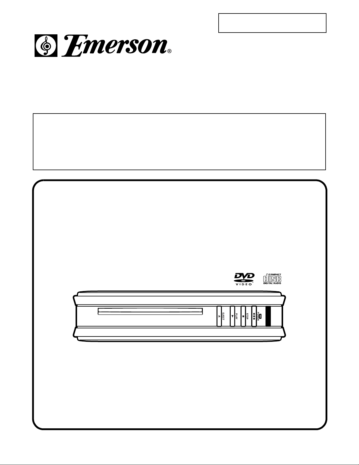
DVD PLAYER
EWD70V5SK
TABLE OF CONTENTS
Cabinet Disassembly Instructions . . . . . . . . . . . . . . . . . . . . . . . . . . . . . . . . . . . . . . . . . . . . . . . . . . 1-1-1
Block Diagrams . . . . . . . . . . . . . . . . . . . . . . . . . . . . . . . . . . . . . . . . . . . . . . . . . . . . . . . . . . . . . . . . 1-2-1
Schematic Diagrams / CBA’s and Test Points . . . . . . . . . . . . . . . . . . . . . . . . . . . . . . . . . . . . . . . . . 1-3-1
Wiring Diagram. . . . . . . . . . . . . . . . . . . . . . . . . . . . . . . . . . . . . . . . . . . . . . . . . . . . . . . . . . . . . . . . . 1-4-1
Packing Exploded View . . . . . . . . . . . . . . . . . . . . . . . . . . . . . . . . . . . . . . . . . . . . . . . . . . . . . . . . . . 1-5-1
Different parts from the original model (EWD70V5) . . . . . . . . . . . . . . . . . . . . . . . . . . . . . . . . . . . . . 1-6-1
Page 2
CABINET DISASSEMBLY INSTRUCTIONS
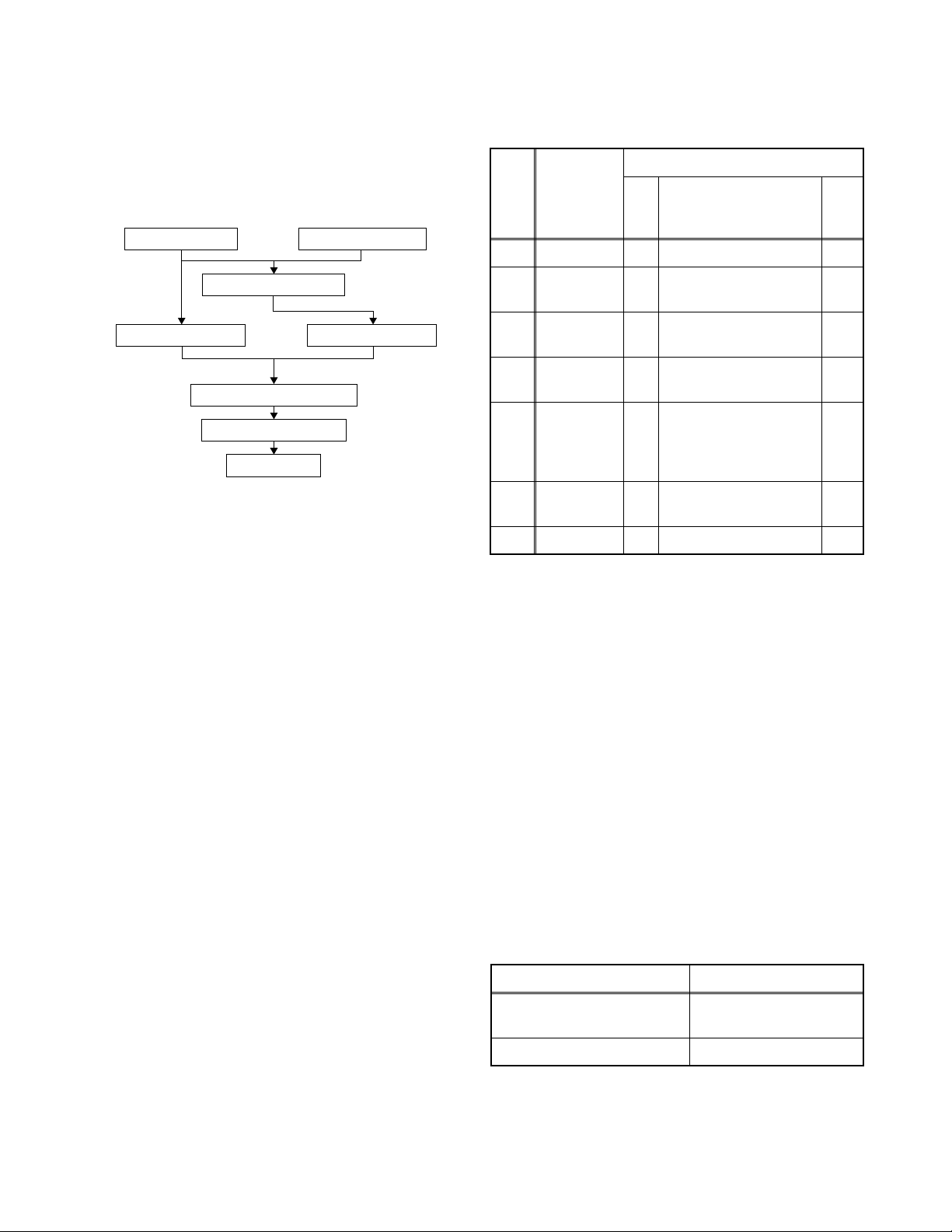
1. Disassembly Flowchart
This flowchart indicates the disassembly steps to gain
access to item(s) to be serviced. When reassembling,
follow the steps in reverse order. Bend, route, and
dress the cables as they were originally.
[1] Top Cover [2] Bottom Cover
[3] Front Assembly
[4] Reinforce Plate [5] Front Bracket
[6] DVD Main CBA Unit
[7] DVD Mechanism
[8] AV CBA
2. Disassembly Method
ID/
Loc.
No.
[1] Top Cover D1 2(S-1) ---
[2]
[3]
[4]
[5]
[6]
[7] AV CBA D4 (S-6), 4(S-7), *3(L-2) ---
↓
(1)
Part
Bottom
Cover
Front
Assembly
Reinforce
Plate
DVD Main
CBA Unit
DVD
Mechanism
↓
(2)
Fig.
No.
D1 2(S-2) ---
D2 *6(L-1) ---
D2 2(S-3) ---
(S-4A), (S-4B),
*CN201, *CN301,
D3
*CN401, *CN601,
*CN801
D3 4(S-5) 2
↓
(3)
Removal
Remove/*Unhook/
Unlock/Release/
Unplug/Desolder
↓
(4)
Note
1
↓
(5)
Note:
(1) Identification (location) No. of parts in the figures
(2) Name of the part
(3) Figure Number for reference
(4) Identification of parts to be removed, unhooked,
unlocked, released, unplugged, unclamped, or
desoldered.
P = Spring, L = Locking Tab, S = Screw,
CN = Connector
* = Unhook, Unlock, Release, Unplug, or Desolder
e.g. 2(S-2) = two Screws (S-2),
2(L-2) = two Locking Tabs (L-2)
(5) Refer to “Reference Notes.”
About tightening screws
When tightening screws, tighten them with the
following torque.
Screws Torque
(S-1), (S-2), (S-3),
(S-4A), (S-5), (S-6), (S-7)
(S-4B) 0.38 ± 0.04 N·m
0.45 ± 0.05 N·m
1-1-1 E61S5DC
Page 3
Reference Notes
1. CAUTION 1: Electrostatic breakdown of the laser
diode in the optical system block may occur as a
potential difference caused by electrostatic charge
accumulated on cloth, human body etc., during
unpacking or repair work.
To avoid damage of pickup follow next procedures.
1) Short the three short lands of FPC cable with
solder before removing the FFC cable (CN201)
from it. If you disconnect the FFC cable
(CN201), the laser diode of pickup will be
destroyed. (Fig. D3)
2) Disconnect Connectors (CN301), (CN401),
(CN601) and (CN801). Remove two Screws
(S-4A) and (S-4B) and lift the DVD Main CBA
Unit. (Fig. D3)
2. CAUTION 2: When reassembling, confirm the
FFC cable (CN201) is connected completely. Then
remove the solder from the three short lands of
FPC cable. (Fig. D3)
3. How to eject a disc in emergency
Press and hold [EJECT] on the unit for more than
5 seconds.
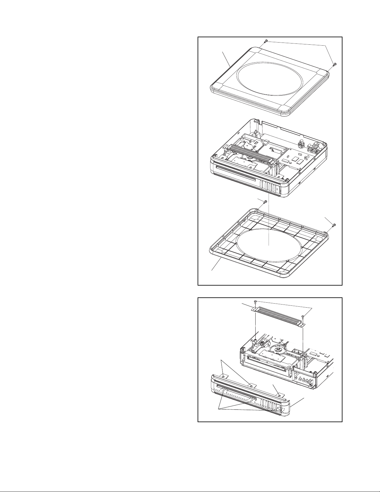
[1] Top Cover
(S-1)
(S-2)
[2] Bottom Cover
[4] Reinforce
Plate
(L-1)
(S-2)
Fig. D1
(S-3)
(L-1)
[3] Front
Assembly
(L-1)
Fig. D2
1-1-2 E61S5DC
Page 4
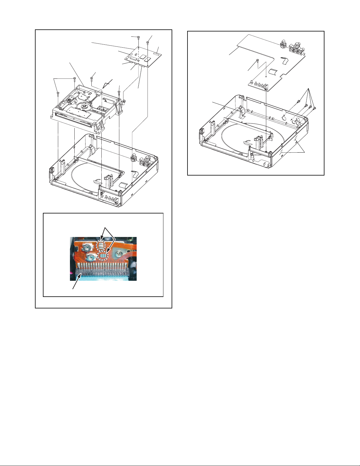
[5] DVD Main
CBA Unit
[6] DVD Mechanism
(S-5)
CN201
(S-5)
(S-4B)
CN301
A
(S-5)
CN801
CN401
(S-4A)
CN601
[7] AV CBA
(S-6)
(S-7)
(L-2)
(L-2)
Fig. D4
Short the three short lands by soldering.
(Either of two places.)
Connector
View for A
Fig. D3
1-1-3 E61S5DC
Page 5

3. How to Eject Manually
< Method 1 >
1. Remove the Bottom Cover.
2. Turn the unit over.
3. Insert the shaft less than a diameter of 3 mm (e.g. screwdriver) straightly into the opening as shown.
4. Turn the shaft along with the opening clockwise.
5. Repeat steps 3 and 4 until the tray will open.
6. Pull the tray slowly manually.
View for B
Rear
Turn the shaft along with
the opening clockwise.
Shaft
(e.g. screwdriver)
Opening
B
Front
Fig. D5-1
1-1-4 E61S5DC
Page 6

< Method 2 >
1. Remove the Bottom Cover.
2. Turn the unit over.
3. Turn the gear A in the direction of the arrow below until the tray will open.
4. Pull the tray slowly manually.
View for B
Gear A
Rear
B
Front
Fig. D5-2
1-1-5 E61S5DC
Page 7

When a disc cannot be ejected by method 1, follow the procedure below and remove the Chassis Cover.
< Method 3 >
1. Remove the Top Cover, the Front Assembly, and
the Reinforce Plate.
2. To remove the Chassis Cover, remove 4 Screws A
as shown in Fig. D6.
3. Remove a disc.
Screws A
Screws A
Chassis
Cover
Disc
Fig. D6
Reassembly note of the Chassis Cover:
1. Insert the pin A on the Chassis Cover into the hole
A on the Main Chassis as shown in Fig. D7.
Chassis Cover
Pin A
Hole A
Main Chassis
2. Tighten 4 Screws A as shown in Fig. D6.
Fig. D7
1-1-6 E61S5DC
Page 8

SCHEMATIC DIAGRAMS / CBA’S AND TEST POINTS
Standard Notes
WARNING
Many electrical and mechanical parts in this chassis
have special characteristics. These characteristics
often pass unnoticed and the protection afforded by
them cannot necessarily be obtained by using
replacement components rated for higher voltage,
wattage, etc. Replacement parts that have these
special safety characteristics are identified in this
manual and its supplements; electrical components
having such features are identified by the mark “#” in
the schematic diagram and the parts list. Before
replacing any of these components, read the parts list
in this manual carefully. The use of substitute
replacement parts that do not have the same safety
characteristics as specified in the parts list may create
shock, fire, or other hazards.
Notes:
1. Do not use the part number shown on these
drawings for ordering. The correct part number is
shown in the parts list, and may be slightly
different or amended since these drawings were
prepared.
2. All resistance values are indicated in ohms
(K = 10
3. Resistor wattages are 1/4W or 1/6W unless
otherwise specified.
4. All capacitance values are indicated in µF
(P = 10
5. All voltages are DC voltages unless otherwise
specified.
3
, M = 106).
-6
µF).
1-3-1 E6N_SC
Page 9

LIST OF CAUTION, NOTES, AND SYMBOLS USED IN THE SCHEMATIC DIAGRAMS ON
THE FOLLOWING PAGES:
1. CAUTION:
FOR CONTINUED PROTECTION AGAINST FIRE HAZARD, REPLACE ONLY WITH THE
F
A V
SAME TYPE FUSE.
ATTENTION: POUR UNE PROTECTION CONTINUE LES RISQES D'INCELE N'UTILISER
QUE DES FUSIBLE DE MÊME TYPE.
RISK OF FIRE-REPLACE FUSE AS MARKED.
This symbol means fast operating fuse.
Ce symbole represente un fusible a fusion rapide.
2. CAUTION:
Fixed Voltage (or Auto voltage selectable) power supply circuit is used in this unit.
If Main Fuse (F1001) is blown, first check to see that all components in the power supply circuit are not
defective before you connect the AC plug to the AC power supply. Otherwise it may cause some components
in the power supply circuit to fail.
3. Note:
1. Do not use the part number shown on the drawings for ordering. The correct part number is shown in the
parts list, and may be slightly different or amended since the drawings were prepared.
2. To maintain original function and reliability of repaired units, use only original replacement parts which are
listed with their part numbers in the parts list section of the service manual.
4. Voltage indications for PLAY and STOP mode on the schematics are as shown below:
2
1
(Unit: Volt)
The same voltage for
both PLAY & STOP modes
5.0
3
5.0
(2.5)
Indicates that the voltage
is not consistent here.
PLAY mode
STOP mode
5. How to read converged lines
1-D3
Distinction Area
Line Number
(1 to 3 digits)
Examples:
1. "1-D3" means that line number "1" goes to the line number
"1" of the area "D3".
2. "1-B1" means that line number "1" goes to the line number
"1" of the area "B1".
3
AREA D3
2
1
ABCD
AREA B1
1-D3
1-B1
6. Test Point Information
: Indicates a test point with a jumper wire across a hole in the PCB.
: Used to indicate a test point with a component lead on foil side.
: Used to indicate a test point with no test pin.
: Used to indicate a test point with a test pin.
1-3-2 E6N_SC
Page 10

PACKING EXPLODED VIEWS
X-5
X-7
X-4
X-3 X-2
X-6
X-1
X-8
S-11
S-2
S-2
S-2
CELLOPHANE TAPE
SET
S-4
X-13
S-1
A-7
1-5-1 E61S5CEX
Page 11

Different parts from the original model (EWD70V5)
Ref. No. Description Part No.
MECHANICAL PARTS
A-2# CHASSIS(WITH SPEAKER) E61S5UD 1VM220721
A-5 MODEL NO LABEL E61S5UD ---------A-8 HOLDER EAS(H9410UD) MAKER NO.EM150DR 0VM415877
S-1 GIFT BOX CARTON E61S5UD 1VM320997
S-2 SIDE PAD E61S0UD 1VM120080C
S-11 SPEACER BOX E61S5UD 1VM320998
X-3# OWNERS MANUAL E61S5UD 1VMN20876
X-13 SPEAKER UNIT ANM5061S5-FA01 USPUSPKHYE05
ELECTRICAL PARTS
AV CBA 1VSA11839
C1050 Not Used
C1354 Not Used
C1361 Not Used
D1030 RECTIFIER DIODE FR202-B/P NDQZ000FR202
L1007 CHOKE COIL 47µH LLBD00PKV022
L1008 PCB JUMPER D0.6-P5.0 JW5.0T
L1009 CHOKE COIL 47µH LLBD00PKV022
L1421 CHIP RES.(1608) 1/10W 0 Ω RRXAZR5Z0000
L1442 CHIP RES.(1608) 1/10W 0 Ω RRXAZR5Z0000
L2031 PCB JUMPER D0.6-P5.0 JW5.0T
Q1004 TRANSISTOR KTC3199-Y-AT/P NQSYKTC3199P
R1023 CHIP RES.(1608) 1/16W F 2.2k Ω RRXGFR5Z0222
R1076 CHIP RES. 1/16W F 1k Ω RRXGFR5Z0102
R1077 METAL OXIDE FILM RES. 2W J 10 Ω RN02100ZU001
R1095 Not Used
R1223 CHIP RES.(1608) 1/10W J 220 Ω RRXAJR5Z0221
R1224 CHIP RES.(1608) 1/10W J 220 Ω RRXAJR5Z0221
R1229 CHIP RES.(1608) 1/10W J 220 Ω RRXAJR5Z0221
R1230 CHIP RES.(1608) 1/10W J 220 Ω RRXAJR5Z0221
R1403 CHIP RES. 1/16W F 160 Ω RRXGFR5Z0161
R1423 CHIP RES. 1/16W F 160 Ω RRXGFR5Z0161
JK1201 PIN JACK 2P MSD-242V-01 NI FE LF JXRL020LY123
JK1203 PHONE JACK MSJ-20000B AG JXSL020LY003
1-6-1 E61S5PL
Page 12

EWD70V5SK
E61S5UD
2005-06-03
 Loading...