

Page 1
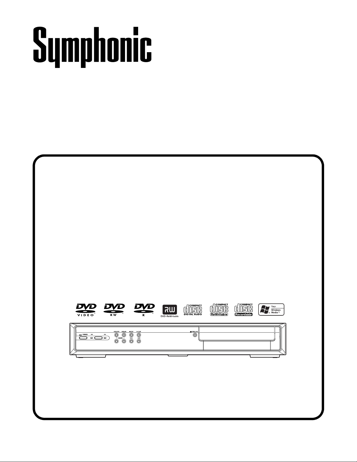
SERVICE MANUAL
DVR(HDD) with DVD Player
CSHP80G
Page 2

IMPORTANT SAFETY NOTICE
Proper service and repair is important to the safe, reliable operation of all
Funai Equipment. The service procedures recommended by Funai and
described in this service manual are effective methods of performing
service operations. Some of these service special tools should be used
when and as recommended.
It is important to note that this service manual contains various CAUTIONS
and NOTICES which should be carefully read in order to minimize the risk
of personal injury to service personnel. The possibility exists that improper
service methods may damage the equipment. It also is important to
understand that these CAUTIONS and NOTICES ARE NOT EXHAUSTIVE.
Funai could not possibly know, evaluate and advice the service trade of all
conceivable ways in which service might be done or of the possible
hazardous consequences of each way. Consequently, Funai has not
undertaken any such broad evaluation. Accordingly, a servicer who uses a
service procedure or tool which is not recommended by Funai must first
use all precautions thoroughly so that neither his safety nor the safe
operation of the equipment will be jeopardized by the service method
selected.
TABLE OF CONTENTS
Specifications . . . . . . . . . . . . . . . . . . . . . . . . . . . . . . . . . . . . . . . . . . . . . . . . . . . . . . . . . . . . . . . . . . . . . . . . . . 1-1-1
Laser Beam Safety Precautions . . . . . . . . . . . . . . . . . . . . . . . . . . . . . . . . . . . . . . . . . . . . . . . . . . . . . . . . . . . . 1-2-1
Important Safety Precautions . . . . . . . . . . . . . . . . . . . . . . . . . . . . . . . . . . . . . . . . . . . . . . . . . . . . . . . . . . . . . . 1-3-1
Standard Notes for Servicing . . . . . . . . . . . . . . . . . . . . . . . . . . . . . . . . . . . . . . . . . . . . . . . . . . . . . . . . . . . . . . 1-4-1
Handling Precautions for HDD . . . . . . . . . . . . . . . . . . . . . . . . . . . . . . . . . . . . . . . . . . . . . . . . . . . . . . . . . . . . . 1-5-1
Cabinet Disassembly Instructions. . . . . . . . . . . . . . . . . . . . . . . . . . . . . . . . . . . . . . . . . . . . . . . . . . . . . . . . . . .1-6-1
How to Self-Check and Initialize the DVR with DVD Player . . . . . . . . . . . . . . . . . . . . . . . . . . . . . . . . . . . . . . . 1-7-1
Firmware Renewal Mode . . . . . . . . . . . . . . . . . . . . . . . . . . . . . . . . . . . . . . . . . . . . . . . . . . . . . . . . . . . . . . . . . 1-8-1
Function Indicator Symbols. . . . . . . . . . . . . . . . . . . . . . . . . . . . . . . . . . . . . . . . . . . . . . . . . . . . . . . . . . . . . . . .1-9-1
Block Diagrams . . . . . . . . . . . . . . . . . . . . . . . . . . . . . . . . . . . . . . . . . . . . . . . . . . . . . . . . . . . . . . . . . . . . . . . . 1-10-1
Schematic Diagrams / CBA’s and Test Points. . . . . . . . . . . . . . . . . . . . . . . . . . . . . . . . . . . . . . . . . . . . . . . . . 1-11-1
Waveforms . . . . . . . . . . . . . . . . . . . . . . . . . . . . . . . . . . . . . . . . . . . . . . . . . . . . . . . . . . . . . . . . . . . . . . . . . . . 1-12-1
Wiring Diagram . . . . . . . . . . . . . . . . . . . . . . . . . . . . . . . . . . . . . . . . . . . . . . . . . . . . . . . . . . . . . . . . . . . . . . . . 1-13-1
System Control Timing Charts . . . . . . . . . . . . . . . . . . . . . . . . . . . . . . . . . . . . . . . . . . . . . . . . . . . . . . . . . . . . 1-14-1
IC Pin Function Descriptions. . . . . . . . . . . . . . . . . . . . . . . . . . . . . . . . . . . . . . . . . . . . . . . . . . . . . . . . . . . . . . 1-15-1
Lead Identifications . . . . . . . . . . . . . . . . . . . . . . . . . . . . . . . . . . . . . . . . . . . . . . . . . . . . . . . . . . . . . . . . . . . . . 1-16-1
Exploded Views. . . . . . . . . . . . . . . . . . . . . . . . . . . . . . . . . . . . . . . . . . . . . . . . . . . . . . . . . . . . . . . . . . . . . . . . 1-17-1
Mechanical Parts List . . . . . . . . . . . . . . . . . . . . . . . . . . . . . . . . . . . . . . . . . . . . . . . . . . . . . . . . . . . . . . . . . . .1-18-1
Electrical Parts List . . . . . . . . . . . . . . . . . . . . . . . . . . . . . . . . . . . . . . . . . . . . . . . . . . . . . . . . . . . . . . . . . . . . . 1-19-1
Manufactured under license from Dolby Laboratories.
“Dolby” and the double-D symbol are trademarks of Dolby Laboratories.
Page 3

SPECIFICATIONS
ITEM
General
DVR Internal 3.5 inch HDD 80 GB
Power consumption 30W (standby: 2.5W)
Recording
Video recording format
Sampling frequency
Compression format
Audio recording format
Sampling frequency
Compression format
Tuner
Receivable channels
VHF
UHF
CATV
Input/Output
Video input
Input level
Jacks
S-Video input
Y (Iuminance) - Input level
C (color) - Input level
Jacks
Audio input
During audio input
Jacks
Component video output
Output level
Jacks
Video output
Output level
Jacks
S-Video output
Y (Iuminance) - Output level
C (color) - Output level
Jack
Audio output
During audio output
Jacks
Digital audio output
Output level
Jack
VHF/UHF antenna
input/output terminal VHF/UHF set 75Ω
13.5MHz
MPEG
48kHz
Dolby Digital
2-13ch
14-69ch
C1-C125ch
Input 1 (rear)
1 Vp-p (75Ω)
RCA jack
Input 1 (rear)
1 Vp-p (75Ω)
286 mVp-p (75Ω)
4 pin mini DIN
Input 1 (rear)
2V rms (47kΩ)
RCA jacks
Y: 1.0 Vp-p (75Ω), P
RCA jacks
1 Vp-p (75Ω)
RCA jack
1 Vp-p (75Ω)
286 mVp-p (75Ω)
4 pin mini DIN
Output 1,2 L/R
2V rms (47kΩ)
RCA jacks
500 mVp-p (75Ω)
RCA jack
B/CB, PR/CR: 0.7 Vp-p (75Ω)
NOTES:
1. All Items are measured without pre-emphasis unless otherwise specified.
2. Power supply: AC120 V 60 Hz
3 Ambient temperature: 5
°C ~ 40 °C
1-1-1 E41A1SP
Page 4
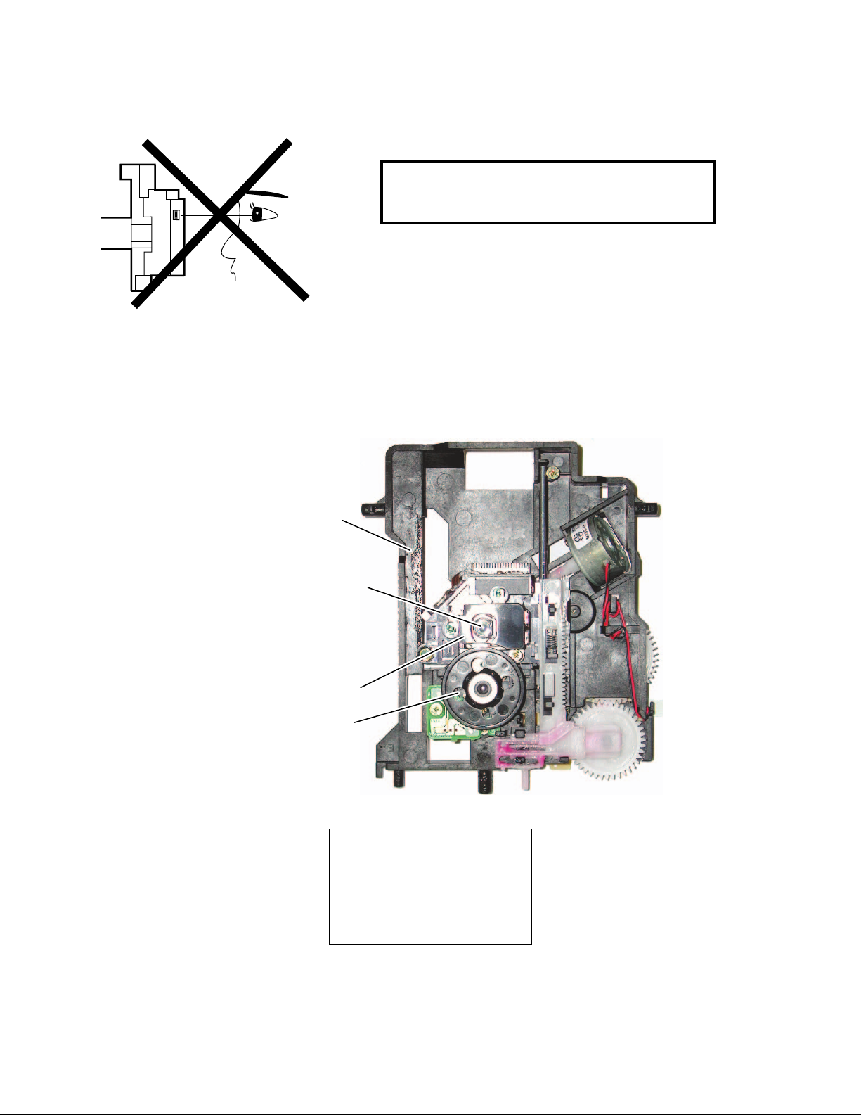
LASER BEAM SAFETY PRECAUTIONS
This DVD player uses a pickup that emits a laser beam.
Do not look directly at the laser beam coming
from the pickup or allow it to strike against your
skin.
The laser beam is emitted from the location shown in the figure. When checking the laser diode, be sure to keep
your eyes at least 30 cm away from the pickup lens when the diode is turned on. Do not look directly at the laser
beam.
CAUTION: Use of controls and adjustments, or doing procedures other than those specified herein, may result in
hazardous radiation exposure.
Drive Mechanism
Assembly
Laser Beam Radiation
Laser Pickup
Turntable
LASER RADIATION
WHEN OPEN. DO NOT
CAUTION
STARE INTO BEAM.
Location: Top of DVD mechanism.
1-2-1 E6NLSP
Page 5

IMPORTANT SAFETY PRECAUTIONS
Product Safety Notice
Some electrical and mechanical parts have special
safety-related characteristics which are often not
evident from visual inspection, nor can the protection
they give necessarily be obtained by replacing them
with components rated for higher voltage, wattage,
etc. Parts that have special safety characteristics are
identified by a # on schematics and in parts lists. Use
of a substitute replacement that does not have the
same safety characteristics as the recommended
replacement part might create shock, fire, and/or other
hazards. The Product’s Safety is under review
continuously and new instructions are issued
whenever appropriate. Prior to shipment from the
factory, our products are carefully inspected to confirm
with the recognized product safety and electrical
codes of the countries in which they are to be sold.
However, in order to maintain such compliance, it is
equally important to implement the following
precautions when a set is being serviced.
Precautions during Servicing
A. Parts identified by the # symbol are critical for
safety. Replace only with part number specified.
B. In addition to safety, other parts and assemblies
are specified for conformance with regulations
applying to spurious radiation. These must also be
replaced only with specified replacements.
Examples: RF converters, RF cables, noise
blocking capacitors, and noise blocking filters, etc.
C. Use specified internal wiring. Note especially:
1) Wires covered with PVC tubing
2) Double insulated wires
3) High voltage leads
D. Use specified insulating materials for hazardous
live parts. Note especially:
1) Insulation tape
2) PVC tubing
3) Spacers
4) Insulators for transistors
E. When replacing AC primary side components
(transformers, power cord, etc.), wrap ends of
wires securely about the terminals before
soldering.
F. Observe that the wires do not contact heat
producing parts (heat sinks, oxide metal film
resistors, fusible resistors, etc.).
G. Check that replaced wires do not contact sharp
edges or pointed parts.
H. When a power cord has been replaced, check that
5 - 6 kg of force in any direction will not loosen it.
I. Also check areas surrounding repaired locations.
J. Be careful that foreign objects (screws, solder
droplets, etc.) do not remain inside the set.
K. Crimp type wire connector
The power transformer uses crimp type
connectors which connect the power cord and the
primary side of the transformer. When replacing
the transformer, follow these steps carefully and
precisely to prevent shock hazards.
Replacement procedure
1) Remove the old connector by cutting the wires
at a point close to the connector.
Important: Do not re-use a connector.
(Discard it.)
2) Strip about 15 mm of the insulation from the
ends of the wires. If the wires are stranded,
twist the strands to avoid frayed conductors.
3) Align the lengths of the wires to be connected.
Insert the wires fully into the connector.
4) Use a crimping tool to crimp the metal sleeve at
its center. Be sure to crimp fully to the complete
closure of the tool.
L. When connecting or disconnecting the internal
connectors, first, disconnect the AC plug from the
AC outlet.
1-3-1 DVDN_ISP
Page 6
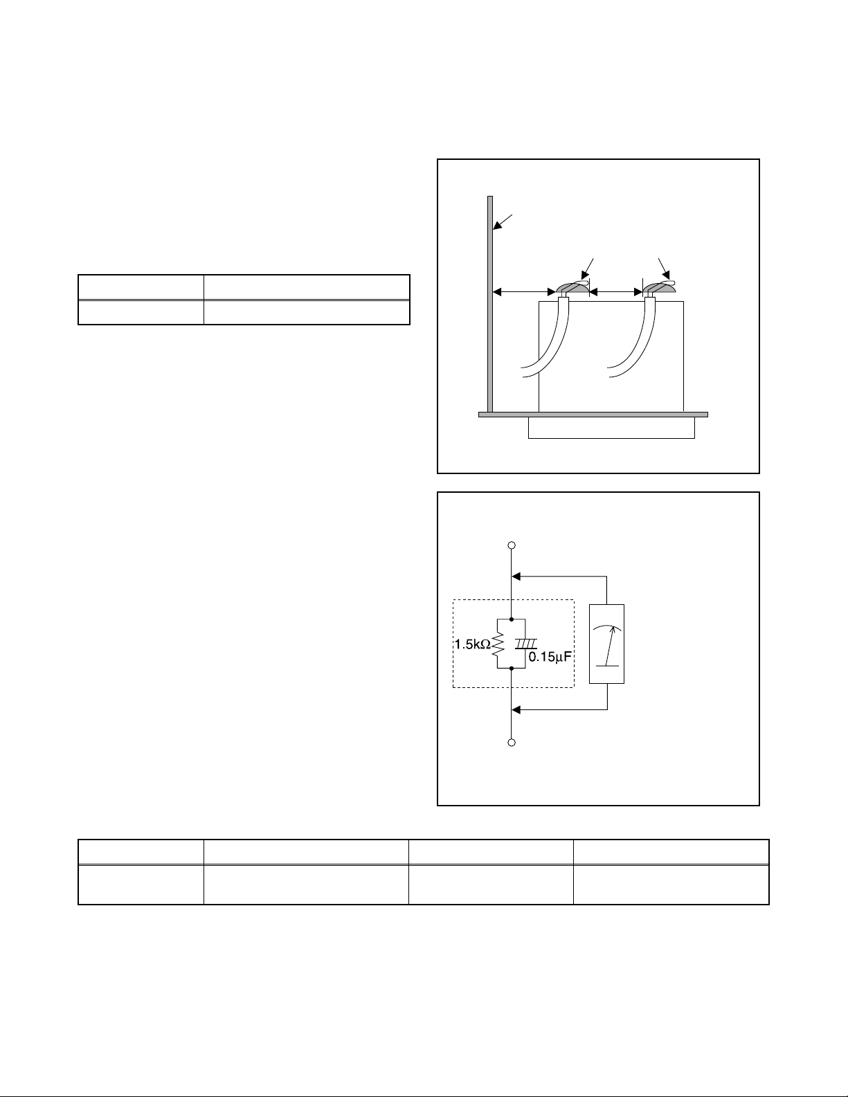
Safety Check after Servicing
Examine the area surrounding the repaired location for damage or deterioration. Observe that screws, parts, and
wires have been returned to their original positions. Afterwards, do the following tests and confirm the specified
values to verify compliance with safety standards.
1. Clearance Distance
When replacing primary circuit components, confirm
specified clearance distance (d) and (d’) between
soldered terminals, and between terminals and
surrounding metallic parts. (See Fig. 1)
Table 1: Ratings for selected area
Chassis or Secondary Conductor
Primary Circuit
AC Line Voltage Clearance Distance (d), (d’)
120 V ≥ 3.2 mm (0.126 inches)
Note: This table is unofficial and for reference only. Be
sure to confirm the precise values.
2. Leakage Current Test
Confirm the specified (or lower) leakage current
between B (earth ground, power cord plug prongs) and
externally exposed accessible parts (RF terminals,
antenna terminals, video and audio input and output
terminals, microphone jacks, earphone jacks, etc.) is
lower than or equal to the specified value in the table
below.
Measuring Method (Power ON):
Insert load Z between B (earth ground, power cord plug
prongs) and exposed accessible parts. Use an AC
voltmeter to measure across the terminals of load Z.
See Fig. 2 and the following table.
d' d
Fig. 1
Exposed Accessible Part
Z
AC Voltmeter
(High Impedance)
Earth Ground
B
Power Cord Plug Prongs
Table 2: Leakage current ratings for selected areas
AC Line Voltage Load Z Leakage Current (i) Earth Ground (B) to:
120 V
Note: This table is unofficial and for reference only. Be sure to confirm the precise values.
0.15 µF CAP. & 1.5 kΩ RES.
Connected in parallel
i ≤ 0.5 mA Peak Exposed accessible parts
1-3-2 DVDN_ISP
Fig. 2
Page 7
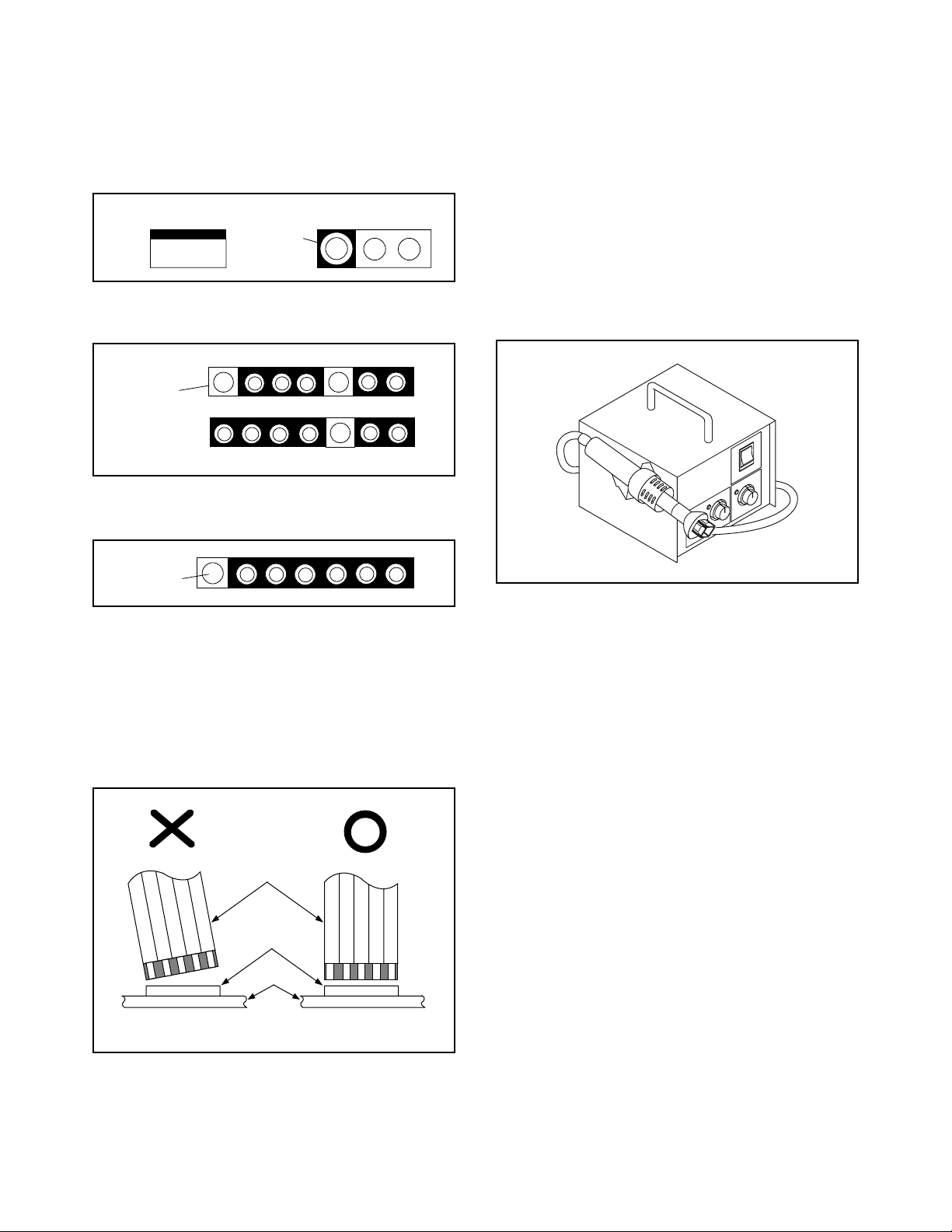
STANDARD NOTES FOR SERVICING
Circuit Board Indications
1. The output pin of the 3 pin Regulator ICs is
indicated as shown.
Top View
Out
2. For other ICs, pin 1 and every fifth pin are
indicated as shown.
Pin 1
3. The 1st pin of every male connector is indicated as
shown.
Pin 1
Input
In
Bottom View
5
10
Pb (Lead) Free Solder
When soldering, be sure to use the Pb free solder.
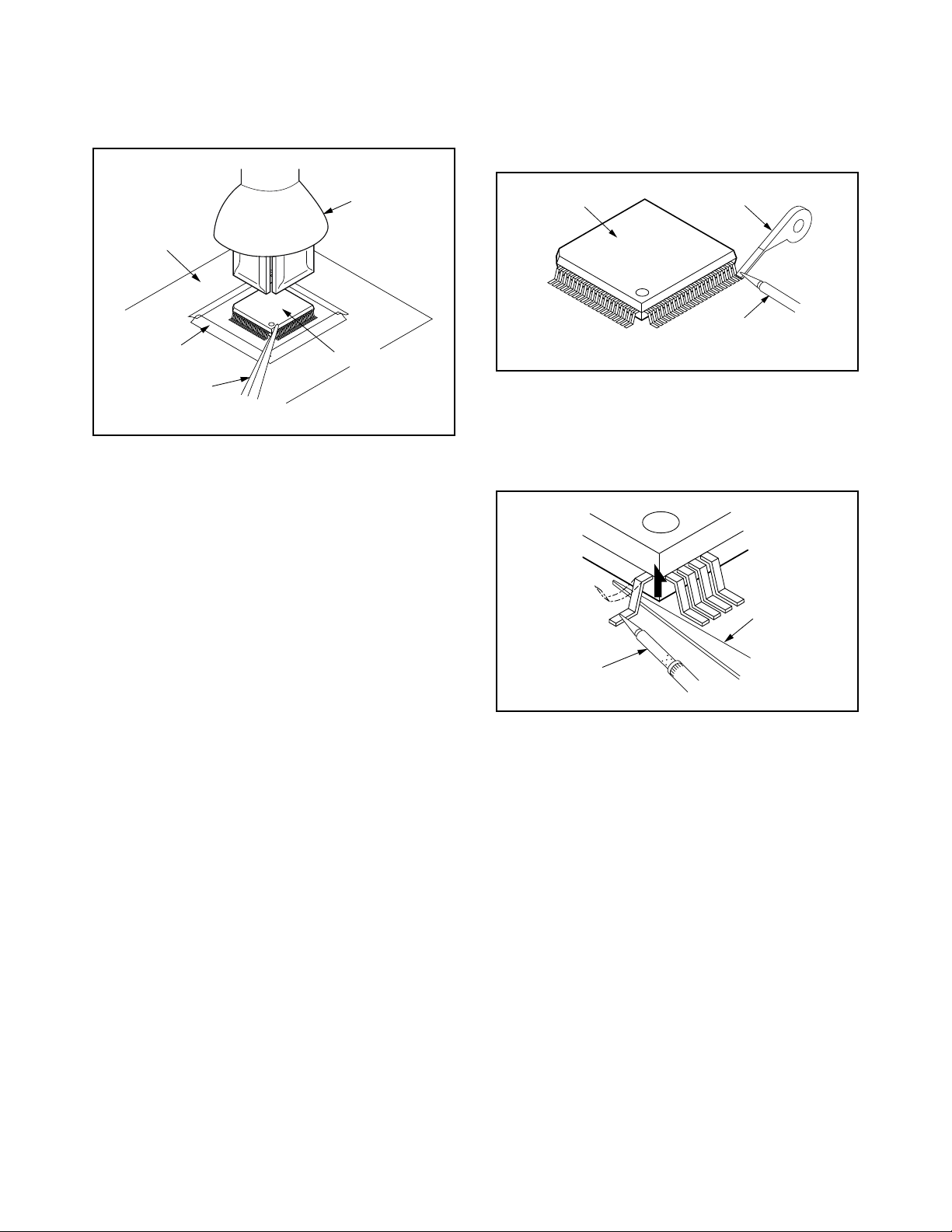
How to Remove / Install Flat Pack-IC
1. Removal
With Hot-Air Flat Pack-IC Desoldering Machine:
1. Prepare the hot-air flat pack-IC desoldering
machine, then apply hot air to the Flat Pack-IC
(about 5 to 6 seconds). (Fig. S-1-1)
Fig. S-1-1
Instructions for Connectors
1. When you connect or disconnect the FFC (Flexible
Foil Connector) cable, be sure to first disconnect
the AC cord.
2. FFC (Flexible Foil Connector) cable should be
inserted parallel into the connector, not at an
angle.
FFC Cable
Connector
CBA
* Be careful to avoid a short circuit.
2. Remove the flat pack-IC with tweezers while
applying the hot air.
3. Bottom of the flat pack-IC is fixed with glue to the
CBA; when removing entire flat pack-IC, first apply
soldering iron to center of the flat pack-IC and heat
up. Then remove (glue will be melted). (Fig. S-1-6)
4. Release the flat pack-IC from the CBA using
tweezers. (Fig. S-1-6)
CAUTION:
1. The Flat Pack-IC shape may differ by models. Use
an appropriate hot-air flat pack-IC desoldering
machine, whose shape matches that of the Flat
Pack-IC.
2. Do not supply hot air to the chip parts around the
flat pack-IC for over 6 seconds because damage
to the chip parts may occur. Put masking tape
around the flat pack-IC to protect other parts from
damage. (Fig. S-1-2)
1-4-1 DVDN_SN
Page 8
3. The flat pack-IC on the CBA is affixed with glue, so
be careful not to break or damage the foil of each
pin or the solder lands under the IC when
removing it.
With Soldering Iron:
1. Using desoldering braid, remove the solder from
all pins of the flat pack-IC. When you use solder
flux which is applied to all pins of the flat pack-IC,
you can remove it easily. (Fig. S-1-3)
CBA
Masking
Tape
Tweezers
Hot-air
Flat Pack-IC
Desoldering
Machine
Flat Pack-IC
Fig. S-1-2
Flat Pack-IC
Desoldering Braid
Soldering Iron
Fig. S-1-3
2. Lift each lead of the flat pack-IC upward one by
one, using a sharp pin or wire to which solder will
not adhere (iron wire). When heating the pins, use
a fine tip soldering iron or a hot air desoldering
machine. (Fig. S-1-4)
Sharp
Pin
Fine Tip
Soldering Iron
3. Bottom of the flat pack-IC is fixed with glue to the
CBA; when removing entire flat pack-IC, first apply
soldering iron to center of the flat pack-IC and heat
up. Then remove (glue will be melted). (Fig. S-1-6)
4. Release the flat pack-IC from the CBA using
tweezers. (Fig. S-1-6)
Fig. S-1-4
1-4-2 DVDN_SN
Page 9
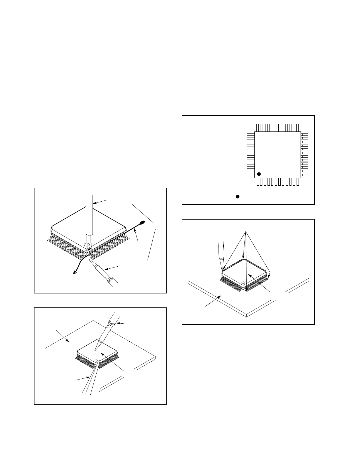
With Iron Wire:
1. Using desoldering braid, remove the solder from
all pins of the flat pack-IC. When you use solder
flux which is applied to all pins of the flat pack-IC,
you can remove it easily. (Fig. S-1-3)
2. Affix the wire to a workbench or solid mounting
point, as shown in Fig. S-1-5.
3. While heating the pins using a fine tip soldering
iron or hot air blower, pull up the wire as the solder
melts so as to lift the IC leads from the CBA
contact pads as shown in Fig. S-1-5.
4. Bottom of the flat pack-IC is fixed with glue to the
CBA; when removing entire flat pack-IC, first apply
soldering iron to center of the flat pack-IC and heat
up. Then remove (glue will be melted). (Fig. S-1-6)
5. Release the flat pack-IC from the CBA using
tweezers. (Fig. S-1-6)
Note: When using a soldering iron, care must be
taken to ensure that the flat pack-IC is not
being held by glue. When the flat pack-IC is
removed from the CBA, handle it gently
because it may be damaged if force is applied.
Hot Air Blower
2. Installation
1. Using desoldering braid, remove the solder from
the foil of each pin of the flat pack-IC on the CBA
so you can install a replacement flat pack-IC more
easily.
2. The “● ” mark on the flat pack-IC indicates pin 1.
(See Fig. S-1-7.) Be sure this mark matches the 1
on the PCB when positioning for installation. Then
presolder the four corners of the flat pack-IC. (See
Fig. S-1-8.)
3. Solder all pins of the flat pack-IC. Be sure that
none of the pins have solder bridges.
Example :
Pin 1 of the Flat Pack-IC
is indicated by a " " mark.
Fig. S-1-7
To Solid
Mounting Point
CBA
Tweezers
Iron Wire
Soldering Iron
Fig. S-1-5
Fine Tip
Soldering Iron
Flat Pack-IC
or
Presolder
Flat Pack-IC
CBA
Fig. S-1-8
Fig. S-1-6
1-4-3 DVDN_SN
Page 10
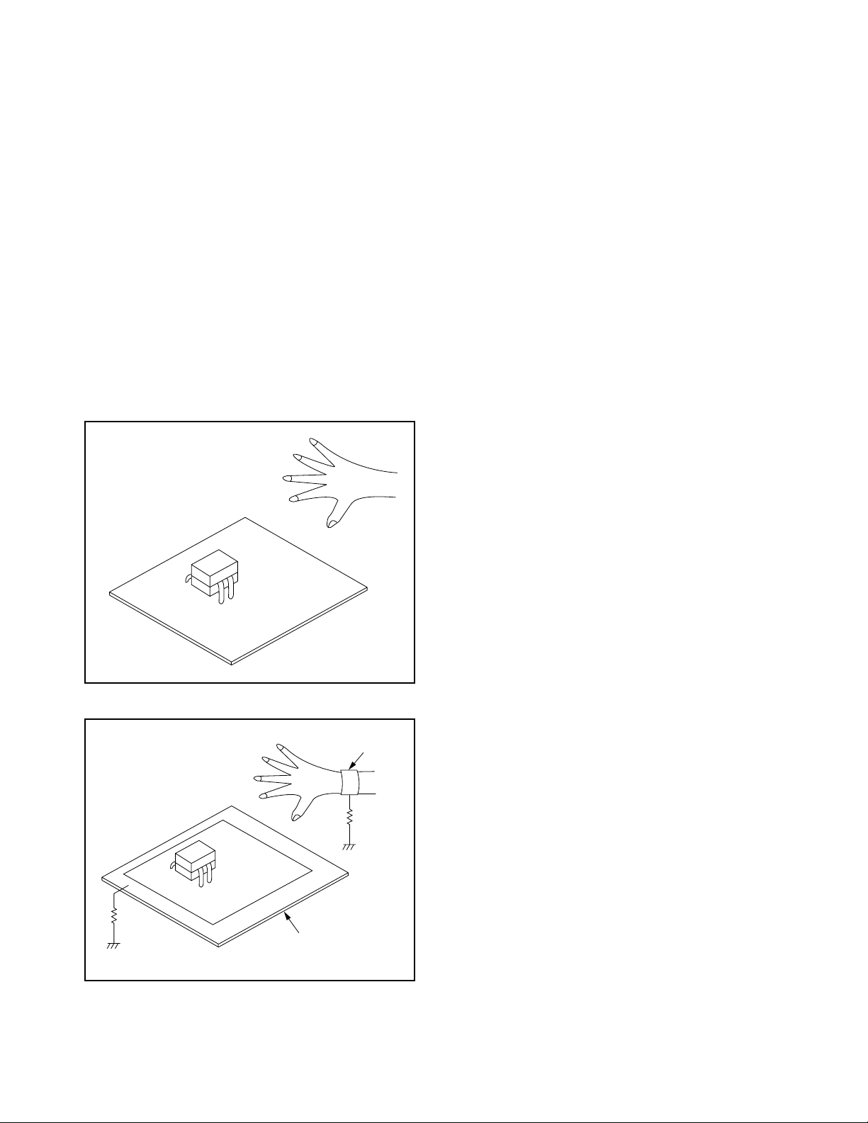
Instructions for Handling Semiconductors
Electrostatic breakdown of the semi-conductors may
occur due to a potential difference caused by
electrostatic charge during unpacking or repair work.
1. Ground for Human Body
Be sure to wear a grounding band (1 MΩ) that is
properly grounded to remove any static electricity that
may be charged on the body.
2. Ground for Workbench
Be sure to place a conductive sheet or copper plate
with proper grounding (1 MΩ) on the workbench or
other surface, where the semi-conductors are to be
placed. Because the static electricity charge on
clothing will not escape through the body grounding
band, be careful to avoid contacting semi-conductors
with your clothing.
<Incorrect>
<Correct>
1MΩ
CBA
Grounding Band
1MΩ
CBA
Conductive Sheet or
Copper Plate
1-4-4 DVDN_SN
Page 11
HANDLING PRECAUTIONS FOR HDD
CAUTION:
1. SHOCK
a. Exposing HDD to shock may be the biggest
damaging factor. Please note that HDD is easily
damaged even if dropped from any height. Be sure
to place HDD on a shock-absorbent mat. Also, be
careful when transporting HDD.
b. Be careful not to subject HDD to any shock when
tightening screws for HDD replacement.
(Tighten screws manually, not with an electric
driver.)
2. MOISTURE
a. Moisture may also be a damaging factor. HDD is
semiclosed style. Sudden changes in ambient
temperature may cause moisture to form. Monitor
temperature and do not allow moisture to form on
the media surface. Also, when opening HDD
package, do so only after package is at ambient
temperature.
b. After replacing HDD, leave it to reach room
temperature (about 2 hours) for preventing dew
internal condensation, and then work necessary
task such as operation check.
4. OTHERS
a. Be careful so as not to do the followings.
Otherwise, HDD might be damaged.
- DO NOT disassemble HDD.
- When handling HDD, be sure to hold both sides
securely.
b. HDD should be stored, packed in the protective
bag, in suitable surroundings (i.e., no extreme
changes in temperature to avoid condensation).
c. When transporting HDD, be sure to use the
exclusive packing case (the replacement HDD
carton).
d. Do not stack HDDs.
e. Do not place vertically because HDD is unstable
and easy to fall.
3. STATIC ELECTRICITY
a. After removing HDD or taking replacement HDD
out of the protective bag (the replacement HDD is
packed in a protective bag), place HDD on a
conductive surface. A grounding band should be
worn when handling.
Grounding Band
Both the conductive surface and grounding band
should be grounded.
b. Make sure that HDD is placed on main unit
completely and then let go of it, when assembling.
c. Do not put HDD on a packing bag. (for preventing
electrostatic damage)
1-5-1 DHDN_SN
Page 12
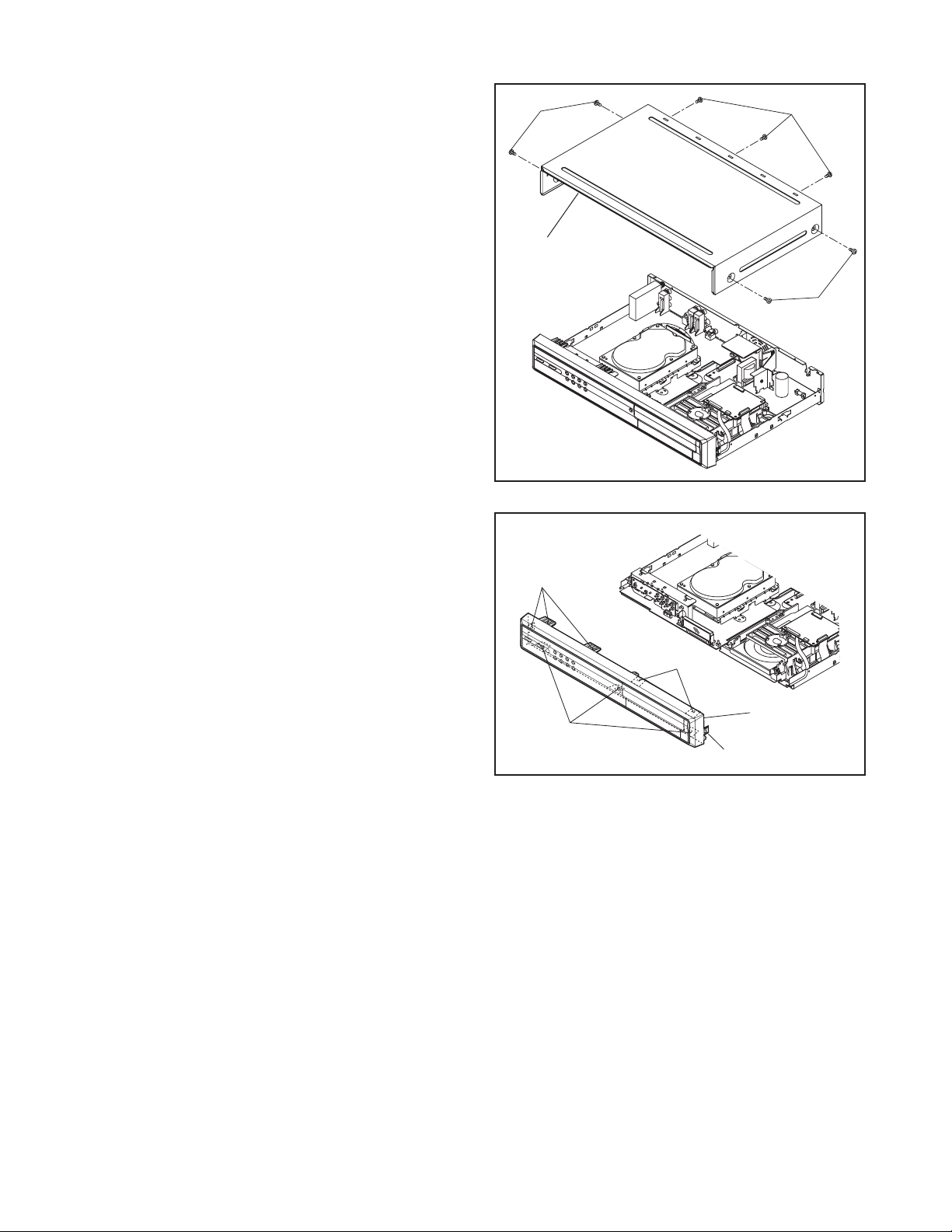
CABINET DISASSEMBLY INSTRUCTIONS
1. Disassembly Flowchart
This flowchart indicates the disassembly steps to gain
access to item(s) to be serviced. When reassembling,
follow the steps in reverse order. Bend, route, and
dress the cables as they were originally.
[1] Top Cover
[15] SW CBA
[16] PCB
Holder
[9] DVD
Main CBA
Unit
[10] DVD
Mechanism
[2] Front
Assembly
[3] HDD
Assembly
[4] DVD
Mechanism &
DVD Main
CBA
[11] Rear
Panel Unit
[12] Fan
Holder
[13] Fan Motor
[14] Rear
Panel
[17] AV CBA
[18] Junction
CBA
[5] HDD Main
CBA Unit
[6] HDD
Bracket
[7] HDD Unit
[8] ATA CBA
ID/
LOC.
No.
[6]
PA RT
HDD
Bracket
REMOVE/*UNHOOK/
Fig.
UNLOCK/RELEASE/
No.
UNPLUG/DESOLDER
Note
D4 4(S-5) ---
[7] HDD Unit D4 ---------- 2
[8] ATA CBA D4 *CN3001, *CN3002 ---
REMOVAL
[9]
[10]
[11]
DVD Main
CBA Unit
DVD
Mechanism
Rear Panel
Unit
2(S-6), *CN201,
D5
*CN301, Earth Plate
D5 ---------- ---
6(S-7), 4(S-8),
D6
*CN1052
[12] Fan Holder D7 2(S-9) --[13] Fan Motor D7 ---------- --[14] Rear Panel D7 ---------- --[15] SW CBA D8 2(S-10), *CN1503 ---
PCB
[16]
Holder
D8 2(S-11) ---
[17] AV CBA D9 3(S-12), *CN2001 ---
Junction
[18]
CBA
D9 *Desolder ---
Power
[19]
Supply
D9 4(S-13) ---
CBA
3
4
---
[19] Power
Supply CBA
2. Disassembly Method
ID/
LOC.
No.
PAR T
Fig.
No.
[1] Top Cover D1 7(S-1) ---
Front
[2]
[3]
Assembly
HDD
Assembly
D2 *6(L-1), *3(L-2) 1
D3
DVD
Mechanism
[4]
& DVD
D3
Main CBA
HDD Main
[5]
CBA Unit
D4 4(S-4), *CN601 ---
REMOVAL
REMOVE/*UNHOOK/
UNLOCK/RELEASE/
UNPLUG/DESOLDER
4(S-2), *CN501,
*CN601, *CN1071
4(S-3), *CN401,
*CN601
Note
---
---
↓
(1)
↓
(2)
↓
(3)
↓
(4)
(5)
Note:
(1): Identification (location) No. of parts in the figures
(2): Name of the part
(3): Figure Number for reference
(4): Identification of parts to be removed, unhooked,
unlocked, released, unplugged, unclamped, or
desoldered.
P=Spring, L=Locking Tab, S=Screw,
CN=Connector
*=Unhook, Unlock, Release, Unplug, or Desolder
e.g. 6(S-1) = six Screws (S-1),
5(L-1) = five Locking Tabs (L-1)
(5): Refer to “Reference Notes.”
↓
1-6-1 E41A1DC
Page 13
Reference Notes
1. Locking Tabs (L-1) and (L-2) are fragile. Be careful
not to break them.
1-1. Release four Locking Tabs (L-1).
1-2. Release three Locking Tabs (L-2) and
remove the Front Assembly.
2. Whenever you have replaced the HDD unit,
initialize the HDD unit. To initialize the HDD unit,
perform the following.
2-1. To put the DVR with DVD Player into the HDD
mode, press the [DVR] button on the remote
control unit.
2-2. To put the DVR with DVD Player into the self-
check mode, after pressing [ANGLE] button,
press the [3], [6], and [9] buttons on the
remote control in that order within three
seconds.
2-3. Press [ENTER] button. The DVR with DVD
Player is initialized and the power is turned
off automatically after two seconds.
3. CAUTION: Electrostatic breakdown of the laser
diode in the optical system block may occur as a
potential difference caused by electrostatic charge
accumulated on cloth, human body etc., during
unpacking or repair work.
To avoid damage of pickup follow next procedures.
3-1. Short the three short lands of FPC cable with
solder before removing the FFC cable
(CN201) from it. If you disconnect the FFC
cable (CN201), the laser diode of pickup will
be destroyed. (Fig. D5)
3-2. Disconnect Connectors (CN301). Remove
two Screws (S-6) with the Earth Plate and
remove the DVD Main CBA Unit. (Fig. D5)
4. CAUTION: When reassembling, confirm the FFC
cable (CN201) is connected completely. Then
remove the solder from the three short lands of
FPC cable. (Fig. D5)
(S-1)
[1] Top Cover
(L-1)
(L-2)
(L-1)
[2] Front
Assembly
(L-1)
(S-1)
(S-1)
Fig. D1
Fig. D2
1-6-2 E41A1DC
Page 14
[3] HDD Assembly
(S-2)
CN601
CN501
CN1071
(S-2)
[7] HDD Unit
[4] DVD Mechanism &
DVD Main CBA
(S-3)
CN401
(S-3)
[8] ATA CBA
CN601
(S-3)
Fig. D3
CN3001
[9] DVD Main CBA Unit
[10] DVD Mechanism
CN301
Short the three short lands by soldering.
(Either of two places.)
FPC Cable
View for A
(S-6)
CN201
(S-6)
Earth Plate
A
(S-5)
(S-4)
CN3002
[6] HDD Bracket
(S-5)
[5] HDD Main CBA Unit
(S-4)
Fig. D4
[11] Rear Panel Unit
CN1052
Fig. D5
(S-8)
(S-7)
(S-8)
(S-8)
Fig. D6
1-6-3 E41A1DC
Page 15
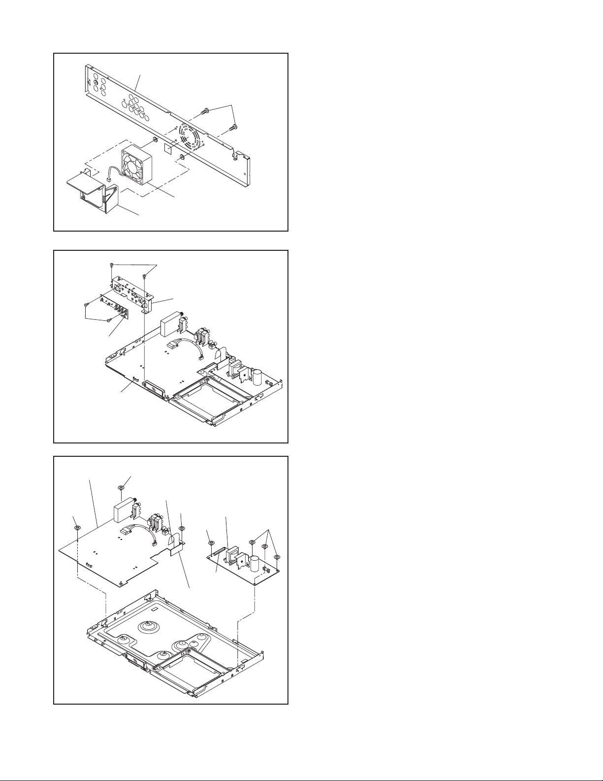
[14] Rear Panel
[13] Fan Motor
(S-9)
(S-10)
[15] SW CBA
CN1503
[17] AV CBA
(S-12)
[12] Fan Holder
(S-11)
[16] PCB Holder
(S-12)
Desolder
(S-12)
[19] Power
Supply CBA
(S-13)
Fig. D7
Fig. D8
(S-13)
CN2001
[18] Junction
CBA
Fig. D9
1-6-4 E41A1DC
Page 16
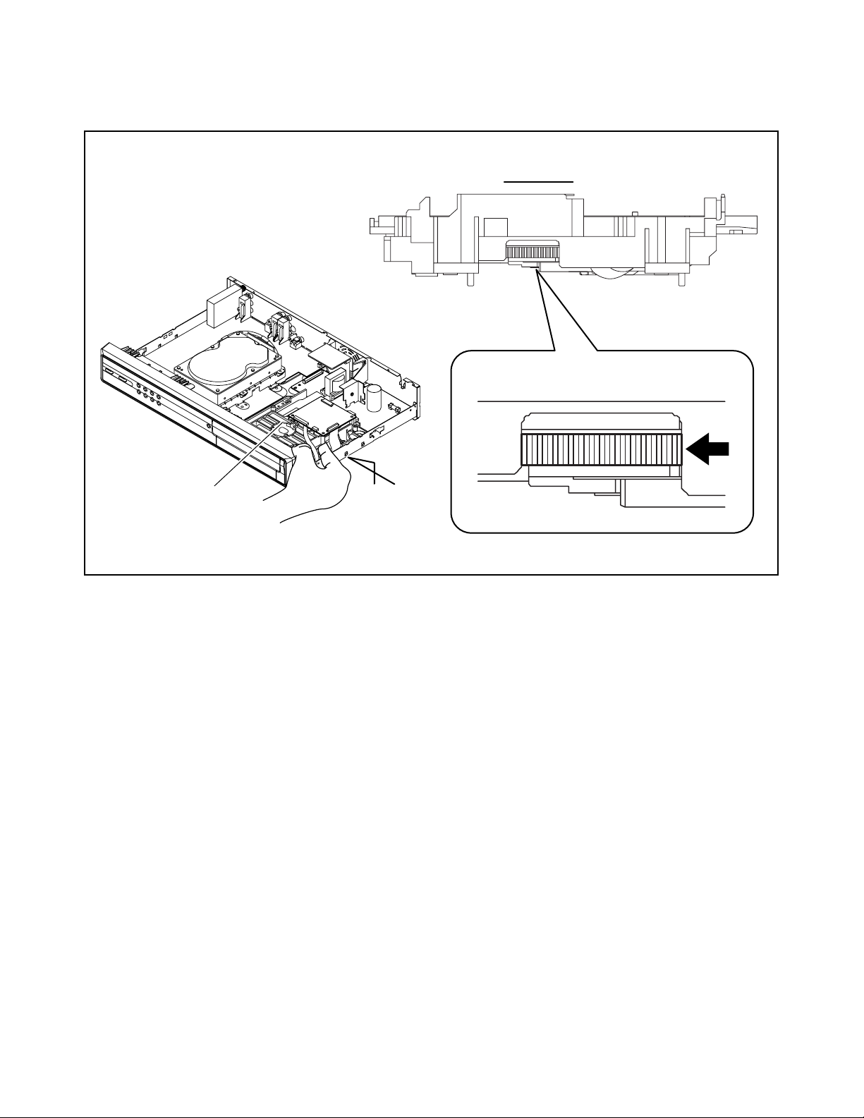
3. How to Eject Manually
1. Remove the Top Cover.
2. Rotate the gear in the direction of the arrow manually as shown below.
View for A
Rotate this roulette in
the direction of the arrow
DVD Mechanism
A
1-6-5 E41A1DC
Page 17
HOW TO SELF-CHECK AND INITIALIZE THE DVR with DVD Player
1. Turn on the DVR with DVD Player recorder.
2. To put the DVR with DVD Player recorder into the HDD mode, press [DVR] on the remote control unit.
3. To put the DVR with DVD Player recorder into the self-check mode, after pressing [ANGLE] button, press the
[3], [6], and [9] buttons on the remote control in that order within three seconds.
Fig. a appears on the screen and all LEDs light.
"
" differs depending on the models.
*******
Self-Analysys and Report
*1
*2
HDD CONNECT STATUS :
HDD POWER ON HOURS :
*3
*4
BE Ver. :
Sub Micon Ver. :
G6*******Q1U
NFQ2B**D1
Fig. a: Self-Check Mode Screen
Table 1: Description of Fig. a
INDICATION DESCRIPTION
HDD CONNECT STATUS (*1) Connecting Condition of HDD
Value of HDD power on hours obtained from S.M.A.R.T. command. (If not obtainable,
HDD POWER ON HOURS (*2)
value of HDD power on hours is “0”.)
Value in parentheses is the factory setting value. (If no setting, the value is “0”.)
BE Ver. (*3) B/E version
Sub Micon Ver. (*4) Sub micro controller version
4. Upon the self-check completion, Fig. b appears on the screen.
"
" differs depending on the models.
*******
Self-Analysys and Report
*5
HDD CONNECT STATUS : OK
HDD POWER ON HOURS : 100(40)
BE Ver. :
Sub Micon Ver. :
*6
*7
FACTORY DEFAULT :
POWER OFF :
G6*******Q1U
NFQ2B**D1
ENTER
POWER
Fig. b: Screen of Finishing Self-Check Mode
Table 2: Indication of HDD self-check (*5)
INDICATION DESCRIPTION
OK Connection of HDD is normal.
NOT FOUND HDD drive cannot be found.
CABLE ERROR FFC cable between the ATA CBA and the HDD drive is not connected correctly.
1-7-1 E41A1INT
Page 18
Table 3: Available button in self-check mode
BUTTON DESCRIPTION
ENTER (*6) Initialize (only when the self-check mode is complete)
POWER (*7) Turn the power off (when the self-check mode is complete)
OTHER Not available
5. When the self-check mode is complete, press [POWER] button to turn the power off.
When initializing the DVR with DVD Player recorder, press [ENTER] button. Fig. c appears on the screen.
After two seconds, the power is turned off automatically.
"
" differs depending on the models.
*******
Self-Analysys and Report
HDD CONNECT STATUS : OK
HDD POWER ON HOURS : 100(40)
BE Ver. :
Sub Micon Ver. :
FACTORY DEFAULT : *8WRITING
G6*******Q1U
NFQ2B**D1
Fig. c: Initialize Mode Screen
Table 4: Description of *8 in Fig. c
INDICATION DESCRIPTION
ENTER Initialization preparation is complete.
WRITING Initializing
OK Initializing is finished normally.
NOTE: When initializing, “Current Clock”, “Setup Changing Item”, “Channel Setup”, “Area Setup”, “Program” and
“HDD Contents” are initialized.
1-7-2 E41A1INT
Page 19
<DVD Section>
FIRMWARE RENEWAL MODE
1. Turn the power on and remove the disc on the tray.
2. To put the unit into version up mode, press [DVD],
[9], [8], [7], [6], and [SEARCH] buttons on the
remote control unit in this order. The tray will open
automatically.
Fig. a appears on the screen and Fig. b appears
on the VFD.
"
" differ depending on the models.
*******
F/W Version Up Mode Model No : *******
Please insert a DISC
for F/W Version Up.
VERSION : *.**
EXIT: POWER
Fig. a Version Up Mode Screen
Fig. b VFD in Version Up Mode
The unit can also enter the version up mode with
the tray open. In this case, Fig. a will be shown on
the screen while the tray is open.
3. Load the disc for version up.
4. The unit enters the F/W version up mode
automatically. Fig. c appears on the screen and
Fig. d appears on the VFD. If you enter the F/W for
different models, “Disc Error” will appear on the
screen, then the tray will open automatically.
"
" differ depending on the models.
*******
(*1)
F/W Version Up Mode Model No : *******
VERSION : ************.ab6
Reading...
VERSION : *.**
No. Appearance State
1 Reading... Sending files into the memory
2 Erasing... Erasing previous version data
3 Programming... Writing new version data
5. After programming is finished, the tray opens
automatically. Fig. e appears on the screen and
the checksum in (*2) of Fig. e appears on the VFD
(Fig. f).
"
" differ depending on the models.
*******
(*2)
F/W Version Up Mode
VERSION : ************.ab6
Completed
SUM : 7ABC
Model No : *******
VERSION : *.**
Fig. e Completed Program Mode Screen
Fig. f VFD upon Finishing the Programming Mode (Example)
At this time, no button is available.
6. Remove the disc on the tray.
7. Unplug the AC cord from the AC outlet. Then plug
it again.
8. Turn the power on by pressing the [POWER]
button and the tray will close.
9. Press [DVD], [1], [2], [3], [4], and [DISPLAY]
buttons on the remote control unit in that order.
Fig. g appears on the screen.
"
" differ depending on the models.
*******
Fig. c Programming Mode Screen
Fig. d VFD in Programming Mode (Example)
The appearance shown in (*1) of Fig. c is
described as follows:
MODEL : *******
Version
Region
: *.**
: *
EXIT: POWEREEPROM CLEAR : CLEAR
Fig. g
1-8-1 E41A1FW
Page 20
10. Press [CLEAR] button on the remote control unit.
Flash Write tab
Fig. h appears on the screen.
"
" differ depending on the models.
*******
MODEL : *******
Version
Region
: *.**
: *
EXIT: POWEREEPROM CLEAR : CLEAR
Fig. h
EEPROM CLEAR : OK
<HDD Section>
When “OK” appears on the screen, the factory
default will be set. Then the firmware renewal
mode is complete.
11. To exit this mode, press [POWER] button.
1. Items necessary to use G6 Serial Firm
Up Software:
G6_SerialFwUp_Ver002.EXE
Save the above file into the local folder.
2. To change to the maintenance mode of
the DVR with DVD Player:
1. Connect the DVR with DVD Player and a PC in
serial.
2. Change the DVR with DVD Player to maintenance
mode.
3. Using the [CHANNEL] up/down buttons on the
remote control, select “4:SERIAL UPDATE” and
press [ENTER] on the remote control.
4. When “Please Press Enter Key” is displayed,
press [ENTER] on the remote control.
5. When the progress bar is displayed, the change is
complete on the DVR with DVD Player.
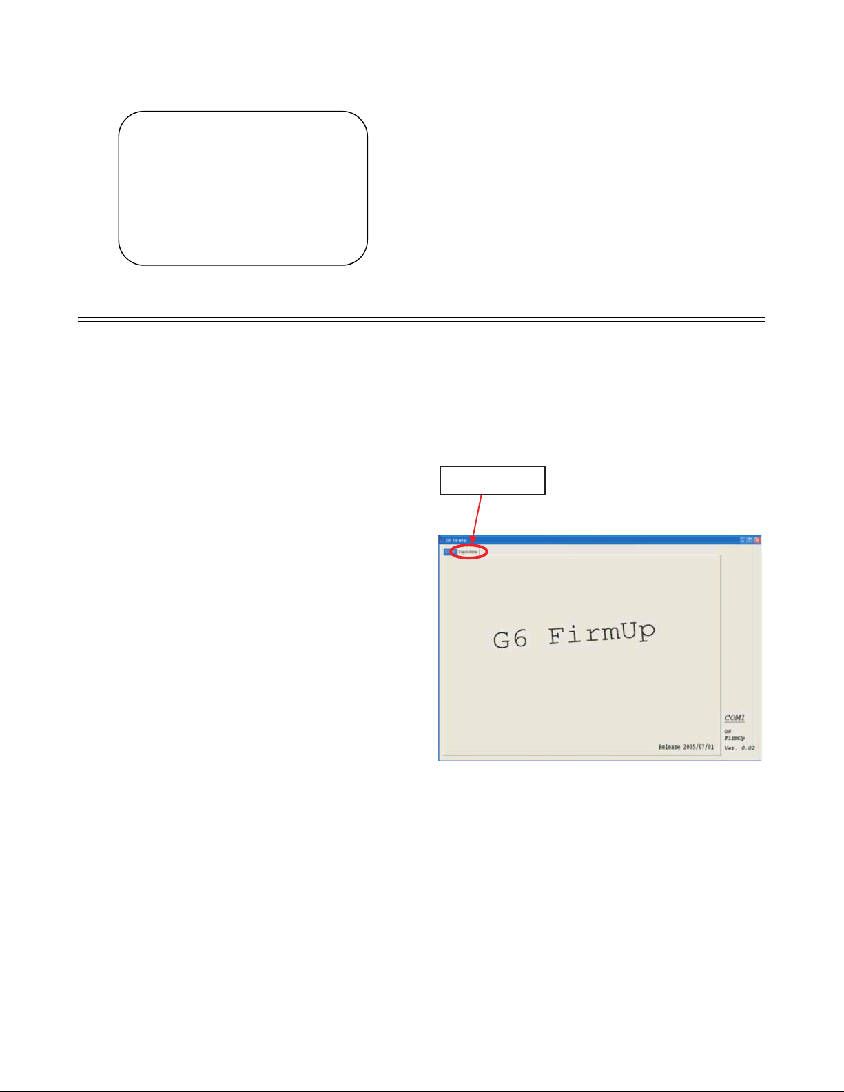
3. To start up the G6 Serial Firm Up
Software:
Com 1 has been selected as the default for the G6
Serial Firm Up Software.
Flash Write tab
Fig. i
1-8-2 E41A1FW
Page 21

4. The progression of the Overwriting
Flash Open button
Flash Write button
process
1. Select the Flash Write tab (See Fig. i), and press
the “File Open” button.
Flash Open button
Flash Write button
Fig. l
4. On completion of the data transfer, the end of data
transfer message “END” will be displayed and the
G6 Serial Firm Up Software can be safely closed.
The data transfer will take approximately 7
minutes.
5. After completion of the data transfer, the DVR with
DVD Player will begin the erase and over writing
process. This process will take approximately 2.5
minutes.
6. When the progress bar of the DVR with DVD
Player turns fully yellow and “STATUS:OK” is
displayed, the overwriting process is complete and
the power can be turned off.
2. When the “File Open” button is pressed, a file
selection screen (as shown below) will appear.
Select the “BIN file” to use for overwriting.
3. After the file selection is complete, press the
“Flash Write” button. File compression and
CHECKSUM will be carried out. The “START”
message will appear. Press the “OK” button to
begin the data transfer.
Fig. j
Fig. k
* When the G6 Serial Firm Up Software is run, the
following may occur but should not be considered a
problem:
1. When a file is selected, the dialog does not
reappear on the screen.
2. The data transfer progress display stops.
1-8-3 E41A1FW
Page 22

FUNCTION INDICATOR SYMBOLS
Note: If an error occurs, a message with the error number appears on the screen.
Recording Error
02-50
Error message
Error No.
Message Error No. Error Description Error Example
Recording
error
System error
03-50
03-56 General error
03-57 Device error
02-50
02-52 Format failure
02-54
02-57 Fan lock
02-59 HDD hang-up
Recording error
caused by media
error
Erasing error (all
titles)
Abnormal HDD
mount
This code is output when recording error caused by media error
occurs, e.g.,stopping recording during attempting to record on a
scratched disc.
This code is output when a number of errors occur:
Ex.1) When Outplay list creation fails.
Ex.2) When the system can’t take the title information which should
be written on the disc.
Ex3) When starting to copy, recording is paused and restarted but,
after the recording pause, recording start fails.
This code is output when an HDD operation error occurs (HDD
recording error), while copying at high speed or constant speed.
This code is output when an error occurs erasing entire VR playlist,
HDD playlist or HDD originals.
This code is output when HDD formatting occurs in maintenance
mode.
This code is output when a [PLAY], [STOP], [REC], [MENU] or [LIST]
button is pressed while HDD is not functional.
This code is output when fan locking (over 30 seconds) is detected.
After the error message is displayed, the power turns off.
This code is output when HDD hang-up event occurs. After the error
message is displayed, the power turns off.
1-9-1 E41A1FIS
Page 23

BLOCK DIAGRAMS
System Control Block Diagram
VFD
BLOCK DIAGRAM
FL2302
TO DVD SYSTEM
CONTROL/SERVO
FAN
TO VIDEO
BLOCK DIAGRAM
TO AUDI O
BLOCK DIAGRAM
IC1502
IC1501
(SUB MICRO CONTROLLER)
EV+3.3V
Q1501
RESET
1 2
14
RESET
PWR-SW
522332
30
P-DOWN
REG-CONT
LOW-POW
EV+5V
Q1502
C1501
(BACKUP CAPACITOR)
7
VCC
VIDEO-SW2
VIDEO-SW1
42
41
FP-DIN
DVD-PLAY
REMOTE-DVD
15
16
REMOTE
DVD-PLAY
VIDEO-SW3
43
FP-CLK
FP-STB
FP-DOUT
(VFD DRIVER)
IC2301
X OUT
X IN
9
8
23
1G
DOUT
DIN
27
28
485049
FL-SDA
XC OUT
12
GRID
~
~
XC IN
11
17
7G
CLK
STB
1
2
FL-SCL
FL-STB
7
a
RE2301
27
REMOTE
SYS-RESET
221918
SEGMENT
~
16
14
~
i
h
SENSOR
REMOTE
SUB-RXD
SUB-TXD
+1.5V-CONT
25
FAN+12V
FAN CONTROL
Q1053, Q1054
53
FAN-CONT1
FAN2FAN-LOCK
1
CN1052
FAN CONTROL
Q1051, Q1052
54
FAN-CONT2
3
FAN-LOCK
AVSEL
AVSEL
HDD-AUDIO-MUTE
37HDD-AUDIO-MUTE
44AVSEL
AUDIO-SW1
AUDIO-SW2
AUDIO-MUTE
38
403933
AUDIO-SW1
AUDIO-SW2
AUDIO-MUTE
SCL
SDA
SCL
SDA
TU1701(TUNER UNIT)
11
12
34
SCL
SDA
KEY-1
KEY-2
DVD-LED
HDD-LED
POWER-LED
1
2
585960
PWR-SW
REG-CONT
TO POWER SUPPLY
BLOCK DIAGRAM
AV CBA
8MHz
RESONATOR
32.768KHz
X1502
X'TAL
IC601
(MAIN MICRO CONTROLLER)
CN1101
26 26SYS-RESET
CN601
A2
SYS-RESET
22 22+1.5V-CONT
25 25SUB-RXD
23 23SUB-TXD
X802
N20
M20
SUB-TXD
SUB-RXD
1-10-1
27MHz
X'TAL
M1
CLK 27 IN
N1
IC501
CLK 27 OUT
EV+2.4VP-ON+1.5V
+1.5V
REGULATOR
HDD MAIN CBA UNIT
EV+5V
D4003
D4002
D4001
CN1503CN4001
POWER-LED
66KEY-1
11DVD-LED
22HDD-LED
33
DVD
Q4003
HDD
Q4002
POWER
Q4001
77KEY-1
KEY SWITCH
KEY SWITCH
SW CBA
E41A1BLS
X1501
LOW-POW
VIDEO-SW1
VIDEO-SW2
VIDEO-SW3
TO VIDEO
BLOCK DIAGRAM
Page 24

DVD System Control/Servo Block Diagram
TO SYSTEM CONTROL
BLOCK DIAGRAM
IC101
(MICRO CONTROLLER)
DVD-AUDIO-MUTE
88
FP-DIN
FP-CLK
FP-STB
FP-DOUT
CN1401
21
22 FP-DOUT
CN401
61
FP-DOUT
TRACKING
RESET73
FOCUS DRIVE
FD-OFST
148
146
DRIVE
TD-OFST
147
139
19
19 FP-CLK1825 DVD-PLAY
20 FP-DIN
59
60
FP-DIN
FP-CLK
SPDL
76
REMOTE-DVD
22
REMOTE-DVD
21 FP-STB2023
82
67
FP-STB
REMOTE-DVD
DVD-PLAY
24
65
DVD-PLAY
SLD
75
SP-ROT
143
81 SL-AMP
AV CBA
TRAY-IN
66
VREF
RESET
IC462
1 3
RESET
IC461
2 1
(SERVO DRIVE)
P-ON+3.3V P-ON+3.3V
1 NOTE:
Either IC461 or IC462 is used for DVD MAIN CBA UNIT.
DVD-AUDIO-MUTE
TO DVD DIGITAL
SIGNAL PROCESS
BLOCK DIAGRAM
IC301
27
-
+
+
FOCUS
ACTUATOR
15
FS(+)
26
-
FS(-)
TO DVD DIGITAL
25
DRIVE
16
TS(+)
SIGNAL PROCESS
24
TS(-)
BLOCK DIAGRAM
-
+
-
+
TRACKING
ACTUATOR
14
DRIVE
13
312
-
+
-
+
SPINDLE
MOTOR
DRIVE
12
11
1
7
14
645
23
IC202
(OP AMP)
3
-
+
6
2
5
13
12
DVD MAIN CBA UNIT
EV+3.3V(D)
SLED
MOTOR
DRIVE
17
18
3SP(+)
4SP(-)
5TRAY-IN
6GND
7SL(-)
CN301
8SL(+)
DRIVE CBA
TRAY-IN
SPINDLE
MOTOR
M
SLED
MOTOR
M
1-10-2
E41A1BLDS
Page 25

HDD Digital Signal Process Block Diagram
TO VIDEO
BLOCK DIAGRAM
DVD-C
HDD-Y
VIDEO-CVBS
HDD-SPDIF
HDD-AUDIO(L)
HDD-AUDIO(R)
151416
L-CHAOBCK
R-CH
HDD-AUDIO-MUTE
MUTE
TO AUDIO
BLOCK DIAGRAM
AUDIO D/A
CONVERTER
AUDIO(L)-IN
AUDIO(R)-IN
1
2
R-CH
L-CH
AUDIO A/D
CONVERTER
REC VIDEO SIGNAL PB VIDEO SIGNAL REC AUDIO SIGNAL PB AUDIO SIGNAL
IC601 (MPEG2 AV CODEC)
J18
D/A
VIDEO
ENCODER
VIDEO
I/F
K18
D/A
W17
VIDEO
DECODER
BACK-END
DIGITAL
SIGNAL
IC901 (AUDIO D/A CONVERTER)
E20
PROCESS
768
AO D ATA
T20
N19
AOSCK
M19
5
AOSCK
U20
4
AOMD
AOMC
V4W4V3
3
2
AOMS
AUDIO
IC902 (AUDIO A/D CONVERTER)
101112
AILRCK
AIBCK
AIDATA
H20
G20
F20
P19
I/F
15
AISCK
FLASH MEMORY
IC604 (FLASH MEMORY)
DDR SDRAM
IC602,IC603 (DDR SDRAM)
HDD MAIN CBA UNIT
CN603CN3001CN3002
ATA CBA
HARD DISK
DRIVE
1-10-3
E41A1BLHD
Page 26

DVD Digital Signal Process Block Diagram
TO
AUDIO
BLOCK
DIAGRAM
AUDIO SIGNAL
DVD-Y
DATA(VIDEO/AUDIO) SIGNAL VIDEO SIGNAL
DATA
RAM
INST.
IC601
(AUDIO D/A CONVERTER)
ROM
DVD-AUDIO(L)
DVD-AUDIO(R)
151416
L-CH
R-CH
4
575686
ADAC-MD
DATA
RAM
DVD-AUDIO-MUTE
MUTE
3
2
ADAC-ML
ADAC-MC
INST.
ROM
AUDIO D/A
CONVERTER
768
5
170
163
PCM-SCLK
171
169
AUDIO
I/F
DVD-SPDIF
177
SERIAL
GENERAL
I/O
INTERRUPT
149
Y
D/A
CONTROLLER
TIMER
TO
DVD-C
158
C
D/A
WATCH DOG
TIMER
VIDEO
BLOCK
DVD-Cr/Pr
152
Cr/Pr
D/A
NTSC/PAL
ENCODER
VIDEO
I/F
REMOTE
CONTROL
DIAGRAM
DVD-Cb/Pb
151
Cb/Pb
D/A
DVD-CVBS
156
CVBS
D/A
32BIT CPU
DATA
INST
RAM
RAM
IC103 (FLASH ROM)
1
~
9
FLASH
~
162548
FADR (0-19)
ROM
~
293638
FDQ (0-15)
~
45
DSP
DECODER
SDRAM ADDRESS(0-11)
~
217
238
SDRAM ADDRESS(0-11)
~~
222629
IC503 (SDRAM) IC101 (MICRO CONTROLLER)
EXTERNAL
MEMORY
I/F
1
2
35
SDRAM
I/O
PROCESSOR
STREAM
I/F
DECODER
I/F
ECC
SDRAM DATA(0-15)
~~
18
252
SDRAM DATA(0-15)
~~
134253
256
114
115
116
DMA
DVD/CD
RF
117
132
CN201
C16
FORMATTER
SIGNAL
PROCESS
131
D18
CIRCUIT
134
133
A17
B15
DETECTOR
UMAC
BCU
129
E14
130
F12
CD/DVD 19
CPU
I/F
READ
MEMORY
32BIT
INST.
ROM
126
AMP
Q253,Q254
CN201
CD-LD 10
CPU
DATA
RAM
124
125
Q251,Q252
AMP
DVD-LD 8
PD-MONI 7
123
6
5
9
GND(LD)
GND(CD-PD)
GND(DVD-PD)
CPU
I/F
WATCH DOG
TIMER
TIMER
INTERRUPT
CONTROLLER
BCU
1 3
CD DVD
DEBUG
23~51
192~212
CD/DVD
83
TO DVD SYSTEM
CONTROL/SERVO
BLOCK DIAGRAM
6
IC201
(SW)
4
FS
TS
FS(+)
CN201
FS(+) 2
FS(-)
FS(-) 3
TS(+)
TS(+) 1
TS(-)
DVD MAIN CBA UNIT
TS(-) 4
PICK-UP
1-10-4
E41A1BLDD
Page 27

Video Block Diagram
JK2202
S-VIDEO
OUT
C
2
1
3 4
Y
REC VIDEO SIGNAL PB VIDEO SIGNAL
5
6
7
DRIVER
DRIVER
2dB
AMP
2dB
AMP
2dB
AMP
LPF DRIVER
LPF
JK2201
WF3
VIDEO-OUT
C1430
VIDEO-Y
JK2203
13
2dB
AMP
LPF DRIVER
OUT
2dB
REAR
VIDEO-Cb/Pb
OUT
VIDEO-Cr/Pr
11
10
AMP
2dB
AMP
LPF DRIVER
LPF DRIVER
OUT
JK2106
MUTE
VIDEO-IN1
8
TUNER
VIDEO
12
VIDEO OUT
TU1701 (TUNER UNIT)
18
TO SYSTEM CONTROL
BLOCK DIAGRAM
4dB
AMP
IC1402 (VIDEO DRIVER)
3
)
3
OUTPUT SELECT
IC1403
(
1
4
WF2
WF1
CN1101
33HDD-Y
CN601
4dB
AMP
1
13
12
11
55HDD-C
17 17VIDEO-CVBS
SW
CTL
IC1401 (VIDEO DRIVER)
9 10
4dB
AMP
3
WF6
4dB
AMP
6
CN1601
CN601
86DVD-Y
4dB
AMP
8
64DVD-Cb/Pb
42DVD-Cr/Pr
31DVD-CVBS
Q1460
10 8DVD-C
AVSEL
TO SYSTEM
CONTROL
BLOCK
DIAGRAM
WF7 WF8
(VIDEO INPUT SELECT)
IC1301
BUFFER
Q1304,
Q1305
LPF
19
CONTROL
LOGIC
VIDEO-SW1
VIDEO-SW2
VIDEO-SW3
24
22 23
AV CBA
HDD-Y
HDD-C
TO HDD
DIGITAL
VIDEO-CVBS
SIGNAL
PROCESS
BLOCK
DIAGRAM
HDD MAIN CBA UNIT
DVD -Y
TO DVD
DVD-Cb/Pb
DVD-Cr/Pr
DIGITAL
SIGNAL
DVD-CVBS
DVD -C
PROCESS
BLOCK
1-10-5
DVD MAIN CBA UNIT
DIAGRAM
E41A1BLV
Page 28

Audio Block Diagram
AUDIO(L)
-OUT1
JK2201
JK2206
REC AUDIO SIGNAL PB AUDIO SIGNAL
DIGITAL
AUDIO OUT
(COAXIAL)
AUDIO(R)
-OUT1
REAR
JK2205
AUDIO(L)
-OUT2
AUDIO(R)
-OUT2
JK2106
AUDIO(L)
-IN1
AUDIO(R)
-IN1
)
(TUNER UNIT)
SIF OUT
TU1701
15
21
SCL
TO SYSTEM CONTROL
BLOCK DIAGRAM
SDA
BUFFER
Q1120
)
4
OUTPUT SELECT
IC1107
(
OP AMP
IC1101
6
3
OUTPUT SELECT
IC1106
MUTE-ONDRIVE
Q1103 Q1101
7
)
OP
AMP
(
6
)
3
13
(
114
12
11
SW
CTL
OP
1
2
Q1102
AMP
MUTE-ON
Q1105
9 10
AUDIO-MUTE
HDD-AUDIO-MUTE
AVSEL
TO
SYSTEM CONTROL
BLOCK DIAGRAM
L-CH
MTS/SAP AUDIO
(
SIGNAL PROCESS
IC1701
11
IN1
TU
(L-CH)
(AUDIO INPUT SELECT)
IC1104
)
OP AMP
(
IC1102
)
OP AMP
(
IC1103
13
2
OP
1
2
OP
1
MTS/SAP
AUDIO
SIGNAL
PROCESS
R-CH
30
29
15
AMP
AMP
24 27
(R-CH)
IN1
4
2
AV CBA
Q1111
OP
OP
3
6
7
6
7
TU
AMP
AMP
SW CTL
9 10
Q1112
AUDIO-SW2
AUDIO-SW1
TO SYSTEM CONTROL
BLOCK DIAGRAM
WF5
WF4
CN1101
HDD-AUDIO(L)
11HDD-SPDIF
13 13
CN601
HDD-SPDIF
HDD-AUDIO(L)
TO HDD
HDD-AUDIO(R)
HDD-AUDIO-MUTE
AUDIO(L)-IN
AUDIO(R)-IN
99
77
11 11
15 15
HDD-AUDIO(R)
HDD-AUDIO-MUTE
AUDIO(L)-IN
AUDIO(R)-IN
DIGITAL
SIGNAL
PROCESS
BLOCK
DIAGRAM
HDD MAIN CBA UNIT
WF10
1-10-6
WF9
CN601 CN1601
TO DVD
DVD-AUDIO(L)
DVD-SPDIF
13 11
18 16
DVD-SPDIF
DVD-AUDIO(L)
DVD-AUDIO(R)
DIGITAL
SIGNAL
PROCESS
DVD-AUDIO(R)
15 13
BLOCK
DIAGRAM
DVD MAIN CBA UNIT
E41A1BLA
Page 29

Power Supply Block Diagram
)
TO HDD
MAIN CBA
UNIT CN501
()
2~4 EV+2.4V
CN1051
+1.2V REG
IC1012
IC1601
NOTE:
The voltage for parts in hot circuit is measured using
hot GND as a common terminal.
P-ON+3.3V
7~8 P-ON+2.5V
12~14
+2.5V REG
IC1011
TO DVD
MAIN CBA
UNIT CN401
(
CN1401
+3.3V REG
1,2 EV+1.2V
3~6 P-ON+3.3V
Q1011
7 P-ON+5V
8,9 EV+10.5V
45617321098567
CN1001
45617321098567
-FL
P-ON+5V
SW+5V
Q1042
F1F2EV+32V
TUNER+5V
VIDEO+5V
CN1002
CN1004
P-ON+10V
Q1041
+10V REG
EV+5V
FAN+12V
EV+3.3V
SW+3.3V
Q1037
+5V REG
Q1031,Q1036
REG
IC1037
SHUNT
TO SYSTEM
CONTROL
BLOCK
REG-CONT
LOW-POW
REGULATOR
Q1032
DIAGRAM
PWR-SW
Q1034
HARD
1 HDD+12V
CN1071
DISK
DRIVE
4 HDD+5V
SW+5V
Q1071
Q1072
"Ce symbole reprèsente un fusible à fusion rapide."
"This symbol means fast operating fuse."
CAUTION !
For continued protection against fire hazard,
replace only with the same type fuse.
ATTENTION : Pour une protection continue les risqes
d'Incele n'utiliser que des fusible de même type.
Risk of fire-replace fuse as marked.
F
A V
T2001
16
3
BRIDGE
RECTIFIER
D2101 - D2104
LINE
FILTER
L2001
JUNCTION
17 17P-ON+12V
8
CBA
REG
IC2204
SHUNT
REGULATOR
Q2203
SW+12V
Q2209
Q2221
9
10
1
4
IC2101
ERROR
7
VOLTAGE DET
IC2201
ERROR
VOLTAGE DET
2
REG
3
CN1005
11LOW-POW
77REG-VCC
55EV+5V
66EV+5V
13
Q2101
33F1
22F2
18 18FAN+12V
19 19EV+2.4V
20 20EV+38V
15 15PWR-SW2
16 16P-ON+12V
12
11
44-FL
CN2001 CN1003
15
14
5
POWER SUPPLY CBA AV CBA
Q2102
F
F2001
1.6A 250V
A V
HOT CIRCUIT. BE CAREFUL.
CAUTION !
Fixed voltage (or Auto voltage selectable) power supply circuit is used in this unit.
If Main Fuse (F2001) is blown , check to see that all components in the power supply
circuit are not defective before you connect the AC plug to the AC power supply.
Otherwise it may cause some components in the power supply circuit to fail.
AC2001
1-10-7
HOT
COLD
E41A1BLP
Page 30

SCHEMATIC DIAGRAMS / CBA’S AND TEST POINTS
Standard Notes
WARNING
Many electrical and mechanical parts in this chassis
have special characteristics. These characteristics
often pass unnoticed and the protection afforded by
them cannot necessarily be obtained by using
replacement components rated for higher voltage,
wattage, etc. Replacement parts that have these
special safety characteristics are identified in this
manual and its supplements; electrical components
having such features are identified by the mark “#” in
the schematic diagram and the parts list. Before
replacing any of these components, read the parts list
in this manual carefully. The use of substitute
replacement parts that do not have the same safety
characteristics as specified in the parts list may create
shock, fire, or other hazards.
Notes:
1. Do not use the part number shown on these
drawings for ordering. The correct part number is
shown in the parts list, and may be slightly
different or amended since these drawings were
prepared.
2. All resistance values are indicated in ohms
(K = 10
3. Resistor wattages are 1/4W or 1/6W unless
otherwise specified.
4. All capacitance values are indicated in µF
(P = 10
5. All voltages are DC voltages unless otherwise
specified.
3
, M = 106).
-6
µF).
1-11-1 G6N_SC
Page 31

LIST OF CAUTION, NOTES, AND SYMBOLS USED IN THE SCHEMATIC DIAGRAMS ON
THE FOLLOWING PAGES:
1. CAUTION:
FOR CONTINUED PROTECTION AGAINST FIRE HAZARD, REPLACE ONLY WITH THE
F
A V
SAME TYPE FUSE.
ATTENTION: POUR UNE PROTECTION CONTINUE LES RISQES D'INCELE N'UTILISER
QUE DES FUSIBLE DE MÊME TYPE.
RISK OF FIRE-REPLACE FUSE AS MARKED.
This symbol means fast operating fuse.
Ce symbole represente un fusible a fusion rapide.
2. CAUTION:
Fixed Voltage (or Auto voltage selectable) power supply circuit is used in this unit.
If Main Fuse (F2001) is blown, first check to see that all components in the power supply circuit are not
defective before you connect the AC plug to the AC power supply. Otherwise it may cause some components
in the power supply circuit to fail.
3. Note:
1. Do not use the part number shown on the drawings for ordering. The correct part number is shown in the
parts list, and may be slightly different or amended since the drawings were prepared.
2. To maintain original function and reliability of repaired units, use only original replacement parts which are
listed with their part numbers in the parts list section of the service manual.
4. Mode: SP/REC
5. Voltage indications for PLAY and REC modes on the schematics are as shown below:
< DVD/HDD Section >
5.0
The same voltage for
both PLAY & STOP modes
5.0
(2.5)
PLAY mode
STOP mode
231
Indicates that the voltage
is not consistent here.
Unit: Volts
6. How to read converged lines
1-D3
Distinction Area
Line Number
(1 to 3 digits)
3
1-B1
AREA D3
2
AREA B1
Examples:
1. "1-D3" means that line number "1" goes to the line number
"1" of the area "D3".
1
1-D3
2. "1-B1" means that line number "1" goes to the line number
"1" of the area "B1".
ABCD
7. Test Point Information
: Indicates a test point with a jumper wire across a hole in the PCB.
: Used to indicate a test point with a component lead on foil side.
: Used to indicate a test point with no test pin.
: Used to indicate a test point with a test pin.
1-11-2 G6N_SC
Page 32

AV 1/5 Schematic Diagram
*1 NOTE
IC1502
R3112N191A-TR-FA
/BU4219G-TR
PST3619NR
Group A Group B
C1509 0.015 0.1
These components (IC1502, C1509)
can be used in any models.
However, you cannot mix components under
Group A with the ones under Group B.
You can choose either Group. The difference
between Group A and Group B is shown below.
1-11-3
E41A1SCAV1
Page 33

AV 2/5 Schematic Diagram
1-11-4
E41A1SCAV2
Page 34

AV 3/5 Schematic Diagram
1-11-5
E41A1SCAV3
Page 35

AV 4/5 Schematic Diagram
1-11-6
E41A1SCAV4
Page 36

AV 5/5 Schematic Diagram
C
TIME
SHIFT
7G 6G 5G 4G 3G 2G 1G
a
b
c
d
e
f
g
c
d
e
ff
g
c
d
e
f
g
c
d
e
f
g
c
d
e
f
g
c
d
e
f
g
hh h
d
f
h
i
a
b
c
d
e
g
a
b
a
b
a
b
a
b
a
b
FL2302 MATRIX CHART
CD
P-SCAN
DVD
PM
DVR
VCR
DB
R
W
7G
PM
h
6G
TIME
SHIFT
5G 4G 3G 2G 1G
P-SCAN
h
c
DB
C
a
d
g
ef
b
h
f
d
CD
VCR
DVR
DVD
R
W
1-11-7
E41A1SCAV5
Page 37

Power Supply & Junction Schematic Diagram
CAUTION !
Fixed voltage (or Auto voltage selectable) power supply circuit is used in this unit.
If Main Fuse (F2001) is blown , check to see that all components in the power supply
circuit are not defective before you connect the AC plug to the AC power supply.
Otherwise it may cause some components in the power supply circuit to fail.
F
A V
CAUTION !
For continued protection against fire hazard,
replace only with the same type fuse.
ATTENTION : Pour une protection continue les risqes
d'Incele n'utiliser que des fusible de même type.
Risk of fire-replace fuse as marked.
"This symbol means fast operating fuse."
"Ce symbole reprèsente un fusible à fusion rapide."
NOTE:
The voltage for parts in hot circuit is measured using
hot GND as a common terminal.
1-11-8
E41A1SCP
Page 38

SW Schematic Diagram
ATA Schematic Diagram
1-11-9
E41A1SCSW
E41A1SCAT
Page 39

DVD Main 1/3 Schematic Diagram
1 NOTE:
Either IC461 or IC462 is used for DVD MAIN CBA UNIT.
1-11-10
E41A1SCD1
Page 40

DVD Main 2/3 Schematic Diagram
1-11-11
E41A1SCD2
Page 41

DVD Main 3/3 Schematic Diagram
1-11-12
E41A1SCD3
Page 42

HDD Main 1/3 Schematic Diagram
NOTE:
1. The order of pins shown in this diagram is different from that of actual IC601.
2. IC601 is divided into six and shown as IC601 (1/6) ~ IC601 (6/6) in this HDD Main Schematic Diagram Section.
1-11-13
E41A1SCH1
Page 43

HDD Main 2/3 Schematic Diagram
NOTE:
1. The order of pins shown in this diagram is different from that of actual IC601.
2. IC601 is divided into six and shown as IC601 (1/6) ~ IC601 (6/6) in this HDD Main Schematic Diagram Section.
1-11-14
E41A1SCH2
Page 44

HDD Main 3/3 Schematic Diagram
NOTE:
1. The order of pins shown in this diagram is different from that of actual IC601.
2. IC601 is divided into six and shown as IC601 (1/6) ~ IC601 (6/6) in this HDD Main Schematic Diagram Section.
1-11-15
E41A1SCH3
Page 45

AV CBA Top View
1-11-16
BE41A0F01011A
Page 46

AV CBA Bottom View
WF4
PIN 13 OF
CN1101
WF2
PIN5 OF
CN1101
WF3
C1430
PLUS LEAD
WF8
PIN 1 OF
CN1601
WF6
PIN 6 OF
CN1601
WF7
PIN 8 OF
CN1601
WF9
PIN 11 OF
CN1601
WF1
PIN 3 OF
CN1101
WF5
PIN 1 OF
CN1101
WF10
PIN 16 OF
CN1601
1-11-17
BE41A0F01011A
Page 47

Power Supply CBA Top View
NOTE:
The voltage for parts in hot circuit is measured using
hot GND as a common terminal.
F
A V
CAUTION !
For continued protection against fire hazard,
replace only with the same type fuse.
ATTENTION : Pour une protection continue les risqes
d'Incele n'utiliser que des fusible de même type.
Risk of fire-replace fuse as marked.
"This symbol means fast operating fuse."
"Ce symbole reprèsente un fusible à fusion rapide."
CAUTION !
Fixed voltage (or Auto voltage selectable) power supply circuit is used in this unit.
If Main Fuse (F2001) is blown , check to see that all components in the power supply
circuit are not defective before you connect the AC plug to the AC power supply.
Otherwise it may cause some components in the power supply circuit to fail.
Because a hot chassis ground is present in the power
supply circut, an isolation transformer must be used.
Also, in order to have the ability to increase the input
slowly, when troubleshooting this type power supply
circuit, a variable isolation transformer is required.
1-11-18
BE4200F01022
Page 48

Power Supply CBA Bottom View
NOTE:
The voltage for parts in hot circuit is measured using
hot GND as a common terminal.
F
A V
CAUTION !
For continued protection against fire hazard,
replace only with the same type fuse.
ATTENTION : Pour une protection continue les risqes
d'Incele n'utiliser que des fusible de même type.
Risk of fire-replace fuse as marked.
"This symbol means fast operating fuse."
"Ce symbole reprèsente un fusible à fusion rapide."
CAUTION !
Fixed voltage (or Auto voltage selectable) power supply circuit is used in this unit.
If Main Fuse (F2001) is blown , check to see that all components in the power supply
circuit are not defective before you connect the AC plug to the AC power supply.
Otherwise it may cause some components in the power supply circuit to fail.
Because a hot chassis ground is present in the power
supply circut, an isolation transformer must be used.
Also, in order to have the ability to increase the input
slowly, when troubleshooting this type power supply
circuit, a variable isolation transformer is required.
1-11-19
BE4200F01022
Page 49

SW CBA Top View
ATA CBA Top View ATA CBA Bottom View
SW CBA Bottom View
Junction CBA
Top View
BE4340F01032
Junction CBA
Bottom View
BE41A0F01011B
1-11-20
BE41A0F01011C
Page 50

WF1
Pin 3 of CN1101
WAVEFORMS
NOTE:
Input: COLOR BAR SIGNAL (WITH 1KHz AUDIO SIGNAL)
WF5
Pin 1 of CN1101
WF9
Pin 11 of CN1601
HDD-Y 0.2V 20µs
WF2
Pin 5 of CN1101
HDD-C 0.2V 20µs
WF3
C1430 PLUS LEAD
HDD-SPDIF 1V 0.1µs
Pin 6 of CN1601
WF7
Pin 8 of CN1601
DVD-AUDIO(L) 0.5V 0.5ms
WF10WF6
Pin 16 of CN1601
20µs0.2VDVD-Y
DVD-SPDIF 1V 0.1µs
VIDEO-CVBS 0.5V 20µs
WF4
Pin 13 of CN1101
HDD-AUDIO(L) 1V 0.5ms
DVD-C 0.2V 20µs
WF8
Pin 1 of CN1601
VIDEO-CVBS 0.5V 20µs
1-12-1
G6NWF
Page 51

4
5
DVD MECHANISM
19
20
CN201
CD/DVD
P-ON+5V
CN601CN1601
GND 75
GND 53
DVD-CVBS 31
DVD-Cb/Pb 64
DVD-Cr/Pr 42
AUDIO(R)
-IN1
AUDIO(L)
-IN1
REAR
VIDEO
-IN1
AV CBA
DETECTOR
17D18
A
GND 97
DVD-Y 86
VIDEO
AUDIO(R)
-OUT1
VIDEO
AUDIO(L)
-OUT1
VIDEO
OUT
S-VIDEO
OUT
236
11
DVD-C 108
GND 119
-Cr/Pr
OUT
-Cb/Pb
OUT
VIDEO-Y
OUT
7
9
11F12
13E14B15C16
GND
VREF
1412
GND 1210
DVD-AUDIO(L) 1311
NU
AUDIO(R)
-OUT2
AUDIO(L)
-OUT2
DIGITAL
AUDIO OUT
WIRING DIAGRAM
SPINDLE
MOTOR
PICK UP
M M
SLED
MOTOR
DVD MAIN
CBA UNIT
P-ON+5V 87
EV+10V 98
EV+10V 109
GND 1110
P-ON+3.3V 76
10
111213141516171819
9
CN1004
10
JW9,
JW10
10
GND8GND9GND
CN1002
GND 1211
123456789
GND1GND2GND
9
10
CD-LD
GND(LD)
DVD-AUDIO(R) 1513
AUDIO+5V 1614
FS TS
4
5
6
7
8
DVD-LD
PD-MONI
GND(DVD-PD)
AUDIO+5V 1715
DVD-SPDIF 1816
CN2001
LOW-POW1F22F13-FL4EV+5V5EV+5V6REG-VCC7GND8GND9GND10GND11GND12GND13SAFETY214PWR-SW215P-ON+12V16P-ON+12V17FAN+12V18EV+2.4V19EV+38V
123456789
1
CN1003
JW7,
JW8
1
CN1001 CN1005
LOW-POW
1
2
FS(-)3TS(-)
TS(+)
FS(+)
GND(CD-PD)
CN401CN1401
EV+1.2V 21
EV+1.2V 32
P-ON+3.3V 54
P-ON+3.3V 43
2345678
3
4
6
F22F1
-FL
EV+5V5EV+5V
P-ON+3.3V 65
7
REG-VCC
GND 1312
3
CN301
GND 1413
GND 1514
4
5
SAFETY2
PWR-SW2
7
8
GND6SL(-)
SL(+)
GND 1615
GND 1716
FP-CLK 1918
DVD-POWER 1817
7
8
FAN+12V
P-ON+12V6P-ON+12V
TRAY-IN
3
4
5
SP(-)
SP(+)
TRAY-IN
FP-STB 2120
FP-DOUT 2221
FP-DIN 2019
POWER SUPPLY
CBA
20
20
JUNCTION
CBA
10
9
10
EV+38V
EV+2.4V
DRIVE CBA
REMOTE-DVD 2322
PWRCON 2423
DVD-PLAY 2524
AC CORD
SW CBA
CN4001
FAN
FAN 1
CN1052
2
FAN-LOCK
DVD-LED1HDD-LED2POWER-LED3GND4EV+5V5KEY-16KEY-2
1
2
CN1503
DVD-LED
HDD-LED
3
4
5
GND
EV+5V
POWER-LED
7
7
KEY-16KEY-2
CN1051
GND 11
CN501
1212
GND 55
EV+2.4V 33
EV+2.4V 44
EV+2.4V 22
P-ON+2.5V 77
GND 66
HDD MAIN
P-ON+2.5V 88
P-ON+2.5V 99
GND 1010
CBA UNIT
P-ON+3.3V 1313
GND 1111
P-ON+3.3V
P-ON+3.3V 1414
GND 1515
NRESET1
GND2
HDD84
HDD73
1245678
CN3001 CN603CN3002
1245678
GND 1616
GND 1717
HDD65
HDD96
CN1101
HDD-SPDIF 11
GND 22
GND 44
HDD-C 55
HDD-Y 33
GND 66
CN601
HDD57
HDD108
HDD49
HDD1110
HDD311
HDD1212
HDD213
HDD1314
HDD115
HDD1416
HDD017
9
1011121314151617183192021222324252627282930313233343536373839
9
1011121314151617183192021222324252627282930313233343536373839
AUDIO(R)-IN 77
HDD1518
ATA
GND 88
GND19
CBA
HARD
AUDIO(L)-IN 99
NU20
DISK
1111
GND 1010
HDD-AUDIO(R)
DMARQ21
DRIVE
1313
1515
1717
GND 1212
HDD-AUDIO(L)
GND 1414
HDD-AUDIO-MUTE
AUDIO+5V 1616
GND 1818
VIDEO-CVBS
GND22
NIOWR23
GND24
NIORD25
GND26
IORDY27
NU28
NDMACK29
2323
2525
GND 2020
RXD1 2121
+1.5V-CONT 2222
SUB-TXD
TXD1 2424
SUB-RXD
NU 1919
GND30
INTRQ31
NU32
SYS-RESET 2626
DA133
NPDIGA34
DA035
DA236
NCS1FX37
NCS3FX38
1-13-1
CN1071
GND 2
GND 3
HDD+5V 4
HDD+12V 1
NDASP39
GND40
40
40
E41A1WI
Page 52

SYSTEM CONTROL TIMING CHARTS
Tray Close ~ Play / Play ~ Tray Open
Tray IN
(TL221)
Sled Drive
(TP303)
Disc Drive
(TP301)
Focus Drive
(TP304)
Tracking Drive
(TP302)
3.3V
0V
1.65V
0V
1.65V
0V
1.65V
0V
1.65V
Tr ay
Close
Disc
Rotation
Play
Disc
Stop
Tr ay
Open
0V
1-14-1 E6NTI
Page 53

IC PIN FUNCTION DESCRIPTIONS
IC1501 (SUB MICROCONTROLLER)
Pin
IN/
No.
OUT
1 IN KEY-1 Front Button Detection 1
2 IN KEY-2 Front Button Detection 2
3 IN FAN-LOCK Fan Failure Detection
4 IN AFT Tuner AFT Power Supply
5 - NU Not Used
6 - EV+3.3V A/D Converter Power Supply
7-VDD Vdd
8 OUT XOUT Clock Output
9 IN XIN Clock Input
10 - GND GND
11 IN XCIN Sub Clock Input
12 OUT XCOUT Sub Clock Output
13 - GND GND
14 IN RESET Reset Signal
15 OUT REMOTE
16 OUT DVD-PLAY DVD Block Control
17 - NU Not Used
18 OUT SUB-TXD B/E Interface
19 IN SUB-RXD B/E Interface
20 - NU Not Used
21 - NU Not Used
22 OUT
23 OUT
24 OUT
25 OUT
26 - NU Not Used
27 IN REMOTE Remote Control Sensor
28 - NU Not Used
29 - NU Not Used
30 IN P-DOWN Power Failure Detection
31 IN USA/JPN
32 OUT LOW-POW Power Consumption Control
IN/
33
OUT
Signal
Name
Output Terminal of Control
DVD by Remote Control
Code
SYSRESET
REGCONT
VIDEOMUTE
+1.5VCONT
SDA IIC BUS Control Data
B/E System Reset
Regulator Control Signal
Video Mute Signal
Main Power Supply Control
USA/JPN Mode Setting,
“L”=JPN/“H”=USA
Function
Pin
IN/
No.
OUT
34 OUT SCL IIC BUS Control Clock
35 - NU Not Used
36 - NU Not Used
37 OUT
38 OUT
39 OUT
40 OUT
41 OUT
42 OUT
43 OUT
44 OUT AVSEL AV Output Mode Contorl
45 - NU Not Used
46 IN PWRCON
47 OUT
48 OUT FL-SDA VFD Control
49 OUT FL-STB VFD Control
50 OUT FL-SCL VFD Control
51 - NU Not Used
52 OUT PWR-SW
53 OUT
54 OUT
55 OUT HDD VFD Control
56 OUT HDD-REC
57 OUT TREC VFD Control
58 OUT DVD-LED
59 OUT HDD-LED
60 OUT
61 - GND GND
Signal
Name
HDDAUDIOMUTE
AUDIOMUTE
AUDIOSW2
AUDIOSW1
VIDEOSW1
VIDEOSW2
VIDEOSW3
DVDPOWER
FANCONT1
FANCONT2
POWERLED
Function
HDD Audio Mute
HDD/DVD Audio Mute
Audio SW Control
Audio SW Control
Video SW Control
Video SW Control
Video SW Control
Monitoring DVD PWRCON
Signal
DVD Power Control Signal
HDD/DVD Power Supply
Control
Fan Rotation Control 1
Fan Rotation Control 2
HDD-REC-LED Output
Signal Control
DVD-LED Output Signal
Control
HDD-LED Output Signal
Control
POWER-LED Output Signal
Control
1-15-1 E41A1PIN
Page 54

Pin
IN/
No.
OUT
62 IN SAFETY1
63 IN SAFETY2
64 IN SAFETY3
Signal
Name
Function
Power Supply Failure
Detection 1
Power Supply Failure
Detection 2
Power Supply Failure
Detection 3
IC2301 (FRONT PANEL CONTROL)
Pin
IN/
No.
OUT
1 IN CLK Clock Input
2 IN STB Serial Interface Strobe
3-K1 Not Used
4 - NU Not Used
5- VSS GND
6 - VDD Power Supply
7OUT a
8OUT b
9OUT c
10 OUT d
11 OUT e
12 IN f
13 IN g
14 OUT h
15 - VEE Pull Down Level
16 OUT i Segment Output
17
18 6G
19 5G
OUT
20 4G
21 3G
22 2G
23 1G
24 - VDD Power Supply
25 - VSS GND
26 IN OSC Oscillator Input
27 Out DOUT Serial Data Output
28 IN DIN Serial Data Input
Signal
7G
Name
Function
Segment Output
Grid Output
1-15-2 E41A1PIN
Page 55

LEAD IDENTIFICATIONS
KRC103M-AT/P
KTA1267Y-AT/P
KTC3199-(GR,BL)-AT/P
E C B
PQ070XF01SZH
GDS
S2Y52
E C B
PT6313-S-TP(L)
28
1
2SA1015-GR(TE2 F T)
2SC2120-(Y)(TE2 F T)
KTC3203-Y-AT/P
KTC3198-GR-AT/P
15
1
2
14
KTC2026-Y/P
BCE
PS2561A-1(W)
1: Anode
4
2: Cathode
3
3: Emitter
4: Collector
RC4580IP
UTC4558
8 5
1 4
2SK3561
GDS
MM1636XWRE
8
1
5
4
E C B
MM1637XVBE
16
1
MN101C77AFG
48
49
64
1
MM1697AJBE
KIA431-AT/P
NC7SB3157P6X
654
KRC102S-RTK/P
C
AN5832SA-E1V
9
24
13
1: R
2: A
123
BE
3: K
123
8
1
33
32
12
BU4219G-TR
R3112N191A-TR-FA
PST3619NR
54
CD4052BNSR
16
9
A: Anode
K: Cathode
Note:
E: Emitter
C: Collector
B: Base
R: Reference
S: Source
17
123
1
8
G: Gate
16
D: Drain
1-16-1 E41A1LE
Page 56

Cabinet
EXPLODED VIEWS
2B7
JW5
2L041
2B1
2L072
2L041
HDD Main CBA Unit
2B4
2L042
2B6
2L071
2L071
2L042
1B3
2L041
ATA CBA
2L042
2L051
2L011
A3
L0-9
DVD Main CBA Unit
2B50
2L051
1B1
Power Supply CBA
2L042
2L011
AC2001
2L011
2L061
2B5
2L042
2L041
A1X
SW CBA
AV CBA
A11
Junction CBA
A2
2L056
A5
2L056
2L056
2B31
FM1001
A5
2B33
2B3
2L011
A12
2B32
2L021
2B33
2L042
2L021
2L011
2L011
A4
A10
A7
1-17-1 E41A1CEX
Page 57

Packing
S2
X2
X1
S2
X5
X10
X3
S3
X20
X4
S10
S1
A7
1-17-2 E41A1PEX
Page 58

MECHANICAL PARTS LIST
PRODUCT SAFETY NOTE: Products marked with a
# have special characteristics important to safety.
Before replacing any of these components, read
carefully the product safety notice in this service
manual. Don't degrade the safety of the product
through improper servicing.
NOTE: Parts that are not assigned part numbers
(---------) are not available.
Ref. No. Description Part No.
A1X FRONT ASSEMBLY E41A1CD 1VM222377
A2 CHASSIS E4200UD 1VM120233
A3 TOP COVER E4200UD 1VM120234
A4 REAR PANEL E41A1CD 1VM222415
A5 FOOT K7010UA 0VM403657A
A7 LABEL BAR CODE HB400UD ---------A10 LABEL (C2) E6700UD NEW ---------A11 LABEL TELEPHONE NO.(SYMPHONIC)
A12 MANUFACTURE LABEL ---------1B1 DVD MECHA E6160(FG LESS) ROHS
1B3 HARD DISK DRIVE HDS728080PLAT20 UHDD809HT001
2B1 HDD BRACKET E4100UD 1VM220761
2B3 FAN HOLDER E4200UD 1VM321120
2B4 PCB HOLDER E4200UD 1VM321121
2B7 TAPE HIMELON(HDD) E4340UD 1VM422058
2B31 RODER PEDESTAL E4100UD 1VM220987
2B32 FAN SPACER E41A0UD 1VM424127
2B33 RUBBER WASHER E41A0UD 1VM424128
2B50 M-PCB EARTH PLATE(G6) E41A0UD 1VM424221
2L011 SCREW C-TIGHT M3X5 BIND HEAD + GBCC3050
2L021 SCREW B-TIGHT M3X8 BIND HEAD+ GBHB3080
2L041 SCREW S-TIGHT M3X6 BIND HEAD+ GBJS3060
2L042 SCREW S-TIGHT M3X6 WASHER HEAD+ GCJS3060
2L051 SCREW P-TIGHT M3*12 BIND+ GBJP3120
2L056 SCREW S-TIGHT M3X8 BIND HEAD+ GBJS3080
2L071 INCH SCREW 3.4X5 + SAC3T050
2L072 SCREW S-TIGHT M3X6 BIND HEAD+ GBJS3060
FM1001 DC FAN MOTOR 2410RL-04W-S20-C01 MMEZR12NM005
JW5 WIRE ASSEMBLY FFC 40P/25MM/PITCH
L0-9 SCREW P-TIGHT M3X8 BIND HEAD+ GBJP3080
E9411UD
N79F0JVM
0.5MM
PACKING
S1 GIFTBOX CARTON E41A1CD 1VM322891
S2 STYROFOAM E4210JD 1VM221622
S3 SET BAG E7708UA 0DM400731D
S10 LABEL EAS L0951UB ----------
ACCESSORIES
X1 REMOTE CONTROL UNIT NB310UD NB310UD
X2 DRY BATTERY R6P/2S XB0M451T0001
X3 RF CABLE 2.5C-2V WPZ0901TM002
X4 ACCESSORY BAG E5700UD 0VM415576
X5 AV CORD WPZ0102TM015 WPZ0102TM015
X10 BAG REMOCON N9430UD(90*250) 0VM411198
X20# OWNERS MANUAL E41A1CD 1VMN22701
----------
N7PF0JVM
WX1E41A0-105
20060317 1-18-1 E41A1CA
Page 59

ELECTRICAL PARTS LIST
PRODUCT SAFETY NOTE: Products marked with a
# have special characteristics important to safety.
Before replacing any of these components, read
carefully the product safety notice in this service
manual. Don't degrade the safety of the product
through improper servicing.
NOTES:
1. Parts that are not assigned part numbers (---------)
are not available.
2. Tolerance of Capacitors and Resistors are noted
with the following symbols.
C.....±0.25% D.....±0.5% F.....±1%
G.....±2% J......±5% K.....±10%
M.....±20% N.....±30% Z.....+80/-20%
DVD MAIN CBA UNIT
Ref. No. Description Part No.
DVD MAIN CBA UNIT N7PFTJUP
HDD MAIN CBA UNIT
Ref. No. Description Part No.
HDD MAIN CBA UNIT 1VSA12717
AV ASSEMBLY
Ref. No. Description Part No.
AV ASSEMBLY
Consists of the following:
AV CBA (AV PCB A)
SW CBA (AV PCB B)
JUNCTION CBA (AV PCB C)
AV CBA
Ref. No. Description Part No.
AV CBA (AV PCB A)
Consists of the following:
CAPACITORS
C1015 ELECTROLYTIC CAP. 100µF/6.3V M CE0KMASDL101
C1016 ELECTROLYTIC CAP. 100µF/6.3V M CE0KMASDL101
C1017 CHIP CERAMIC CAP.(1608) F Z 0.1µF/50V CHD1JZ30F104
C1018 CHIP CERAMIC CAP.(1608) F Z 0.1µF/50V CHD1JZ30F104
C1031 CHIP CERAMIC CAP.(1608) B K 0.01µF/50V CHD1JK30B103
C1032 CHIP CERAMIC CAP.(1608) B K 0.01µF/50V CHD1JK30B103
C1033 ELECTROLYTIC CAP. 100µF/6.3V M H7 CE0KMASSL101
C1034 CHIP CERAMIC CAP.(1608) B K 0.01µF/50V CHD1JK30B103
C1035 ELECTROLYTIC CAP. 470µF/6.3V M CE0KMASDL471
C1041 ELECTROLYTIC CAP. 470µF/16V M CE1CMASDL471
C1042 ELECTROLYTIC CAP. 47µF/16V M CE1CMASDL470
C1043 ELECTROLYTIC CAP. 100µF/6.3V M CE0KMASDL101
C1044 ELECTROLYTIC CAP. 470µF/6.3V M CE0KMASDL471
C1050 CHIP CERAMIC CAP.(1608) B K 0.1µF/25V CHD1EK30B104
C1051 CHIP CERAMIC CAP.(1608) B K 0.1µF/25V CHD1EK30B104
C1052 ELECTROLYTIC CAP. 100µF/16V M CE1CMASDL101
1VSA12398
----------
----------
----------
----------
Ref. No. Description Part No.
C1071 ELECTROLYTIC CAP. 1000µF/6.3V M CE0KMASDL102
C1072 ELECTROLYTIC CAP. 1000µF/6.3V M CE0KMASDL102
C1074 ELECTROLYTIC CAP. 100µF/6.3V M CE0KMASDL101
C1075 CHIP CERAMIC CAP.(1608) F Z 0.1µF/50V CHD1JZ30F104
C1076 ELECTROLYTIC CAP. 100µF/6.3V M CE0KMASDL101
C1081 CHIP CERAMIC CAP.(1608) F Z 0.1µF/50V CHD1JZ30F104
C1082 ELECTROLYTIC CAP. 100µF/6.3V M CE0KMASDL101
C1101 ELECTROLYTIC CAP. 10µF/16V M CE1CMASDL100
C1102 ELECTROLYTIC CAP. 10µF/16V M CE1CMASDL100
C1103 ELECTROLYTIC CAP. 10µF/16V M CE1CMASDL100
C1104 ELECTROLYTIC CAP. 10µF/16V M H7 CE1CMASSL100
C1105 CHIP CERAMIC CAP.(1608) CH J 270pF/50V CHD1JJ3CH271
C1106 CHIP CERAMIC CAP.(1608) CH J 270pF/50V CHD1JJ3CH271
C1107 CHIP CERAMIC CAP.(1608) CH J 33pF/50V CHD1JJ3CH330
C1108 CHIP CERAMIC CAP.(1608) CH J 33pF/50V CHD1JJ3CH330
C1121 ELECTROLYTIC CAP. 10µF/16V M CE1CMASDL100
C1122 ELECTROLYTIC CAP. 10µF/16V M CE1CMASDL100
C1130 ELECTROLYTIC CAP. 470µF/6.3V M CE0KMASDL471
C1132 ELECTROLYTIC CAP. 47µF/16V M CE1CMASDL470
C1133 CHIP CERAMIC CAP.(1608) F Z 0.1µF/50V CHD1JZ30F104
C1134 CHIP CERAMIC CAP.(1608) F Z 0.1µF/50V CHD1JZ30F104
C1140 CHIP CERAMIC CAP.(1608) F Z 0.1µF/50V CHD1JZ30F104
C1150 ELECTROLYTIC CAP. 100µF/16V M CE1CMASDL101
C1151 CHIP CERAMIC CAP.(1608) CH J 33pF/50V CHD1JJ3CH330
C1152 CHIP CERAMIC CAP.(1608) CH J 33pF/50V CHD1JJ3CH330
C1153 ELECTROLYTIC CAP. 10µF/16V M CE1CMASDL100
C1154 ELECTROLYTIC CAP. 10µF/16V M CE1CMASDL100
C1157 ELECTROLYTIC CAP. 10µF/16V M CE1CMASDL100
C1158 ELECTROLYTIC CAP. 10µF/16V M CE1CMASDL100
C1159 CHIP CERAMIC CAP.(1608) F Z 0.1µF/50V CHD1JZ30F104
C1160 ELECTROLYTIC CAP. 220µF/16V M CE1CMASDL221
C1161 ELECTROLYTIC CAP. 470µF/6.3V M CE0KMASDL471
C1162 CHIP CERAMIC CAP.(1608) F Z 0.1µF/50V CHD1JZ30F104
C1163 CHIP CERAMIC CAP.(1608) F Z 0.1µF/50V CHD1JZ30F104
C1175 ELECTROLYTIC CAP. 10µF/16V M CE1CMASDL100
C1176 ELECTROLYTIC CAP. 10µF/16V M CE1CMASDL100
C1191 ELECTROLYTIC CAP. 470µF/6.3V M CE0KMASDL471
C1210 CHIP CERAMIC CAP. CH J 15pF/50V CHD1JJ3CH150
C1212 CHIP CERAMIC CAP.(1608) F Z 0.1µF/50V CHD1JZ30F104
C1214 ELECTROLYTIC CAP. 47µF/6.3V M CE0KMASDL470
C1303 CHIP CERAMIC CAP.(1608) F Z 0.1µF/50V CHD1JZ30F104
C1313 CHIP CERAMIC CAP.(1608) B K 0.01µF/50V CHD1JK30B103
C1314 ELECTROLYTIC CAP. 22µF/16V M CE1CMASDL220
C1315 ELECTROLYTIC CAP. 100µF/6.3V M CE0KMASDL101
C1316 CHIP CERAMIC CAP.(1608) F Z 0.1µF/50V CHD1JZ30F104
C1334 CHIP CERAMIC CAP.(1608) F Z 0.1µF/50V CHD1JZ30F104
C1338 CHIP CERAMIC CAP.(1608) CH J 33pF/50V CHD1JJ3CH330
C1407 ELECTROLYTIC CAP. 1µF/50V M CE1JMASDL1R0
C1408 ELECTROLYTIC CAP. 1µF/50V M CE1JMASDL1R0
C1409 ELECTROLYTIC CAP. 1µF/50V M CE1JMASDL1R0
C1417 CHIP CERAMIC CAP.(1608) F Z 0.1µF/50V CHD1JZ30F104
C1421 ELECTROLYTIC CAP. 1000µF/6.3V M CE0KMASDL102
C1422 ELECTROLYTIC CAP. 1000µF/6.3V M CE0KMASDL102
C1423 ELECTROLYTIC CAP. 470µF/6.3V M CE0KMASDL471
C1424 ELECTROLYTIC CAP. 470µF/6.3V M CE0KMASDL471
C1430 ELECTROLYTIC CAP. 470µF/6.3V M CE0KMASDL471
C1431 ELECTROLYTIC CAP. 1µF/50V M CE1JMASDL1R0
C1432 CHIP CERAMIC CAP.(1608) B K 0.01µF/50V CHD1JK30B103
C1433 CHIP CERAMIC CAP.(1608) B K 0.01µF/50V CHD1JK30B103
C1434 CHIP CERAMIC CAP.(1608) B K 0.33µF/10V CHD1AK30B334
20060317 1-19-1 E41A1EL
Page 60

Ref. No. Description Part No.
C1435 CHIP CERAMIC CAP.(1608) B K 0.01µF/50V CHD1JK30B103
C1436 CHIP CERAMIC CAP.(1608) B K 0.33µF/10V CHD1AK30B334
C1460 CHIP CERAMIC CAP.(1608) F Z 0.1µF/50V CHD1JZ30F104
C1470 CHIP CERAMIC CAP.(1608) F Z 0.1µF/50V CHD1JZ30F104
C1471 CHIP CERAMIC CAP.(1608) B K 0.01µF/50V CHD1JK30B103
C1472 ELECTROLYTIC CAP. 22µF/16V M CE1CMASDL220
C1480 CHIP CERAMIC CAP.(1608) F Z 0.1µF/50V CHD1JZ30F104
C1481 CHIP CERAMIC CAP.(1608) F Z 0.1µF/50V CHD1JZ30F104
C1482 CHIP CERAMIC CAP.(1608) B K 0.01µF/50V CHD1JK30B103
C1483 ELECTROLYTIC CAP. 22µF/16V M CE1CMASDL220
C1490 ELECTROLYTIC CAP. 100µF/6.3V M CE0KMASDL101
C1501 ELECTROLYTIC CAP. 1000µF/6.3V M CE0KMASDL102
C1502 CHIP CERAMIC CAP.(1608) F Z 0.1µF/50V CHD1JZ30F104
C1503 CHIP CERAMIC CAP.(1608) F Z 0.1µF/50V CHD1JZ30F104
C1506 CHIP CERAMIC CAP.(1608) CH J 22pF/50V CHD1JJ3CH220
C1507 CHIP CERAMIC CAP. CH J 18pF/50V CHD1JJ3CH180
C1508 CHIP CERAMIC CAP.(1608) F Z 0.1µF/50V CHD1JZ30F104
If C1509 is 0.015µF, then IC1502 is BU4219G-TR or R3112N191A-TR-FA.
C1509 CHIP CERAMIC CAP.(1608) B K 0.015µF/50V CHD1JK30B153
IC1502 VOLTAGE DETECT R3112N191A-TR-FA or QSZBA0TRC021
RESET IC BU4219G-TR QSZBA0TRM090
If C1509 is 0.1µF, then IC1502 is PST3619NR.
C1509 CHIP CERAMIC CAP.(1608) B K 0.1µF/25V CHD1EK30B104
IC1502 SYSTEM RESET IC PST3619NR QSZBA0TMM151
C1510 CHIP CERAMIC CAP.(1608) CH J 1000pF/50V CHD1JJ3CH102
C1513 CHIP CERAMIC CAP.(1608) CH J 100pF/50V CHD1JJ3CH101
C1516 CHIP CERAMIC CAP.(1608) CH J 100pF/50V CHD1JJ3CH101
C1518 CHIP CERAMIC CAP.(1608) B K 1000pF/50V CHD1JK30B102
C1519 CHIP CERAMIC CAP.(1608) B K 1000pF/50V CHD1JK30B102
C1520 CHIP CERAMIC CAP.(1608) CH J 100pF/50V CHD1JJ3CH101
C1521 CHIP CERAMIC CAP.(1608) CH J 100pF/50V CHD1JJ3CH101
C1524 CHIP CERAMIC CAP.(1608) CH J 100pF/50V CHD1JJ3CH101
C1525 CHIP CERAMIC CAP.(1608) CH J 100pF/50V CHD1JJ3CH101
C1601 CHIP CERAMIC CAP.(1608) F Z 0.1µF/50V CHD1JZ30F104
C1602 CHIP CERAMIC CAP.(1608) B K 0.1µF/25V CHD1EK30B104
C1603 CHIP CERAMIC CAP. F Z 1µF/10V CHD1AZ30F105
C1604 ELECTROLYTIC CAP. 470µF/6.3V M CE0KMASDL471
C1701 ELECTROLYTIC CAP. 1000µF/6.3V M CE0KMASDL102
C1702 CHIP CERAMIC CAP.(1608) F Z 0.1µF/50V CHD1JZ30F104
C1703 ELECTROLYTIC CAP. 100µF/6.3V M CE0KMASDL101
C1704 CHIP CERAMIC CAP.(1608) CH J 47pF/50V CHD1JJ3CH470
C1706 CHIP CERAMIC CAP.(1608) B K 0.033µF/50V CHD1JK30B333
C1708 ELECTROLYTIC CAP. 1µF/50V M CE1JMASDL1R0
C1709 CHIP CERAMIC CAP.(1608) F Z 0.1µF/50V CHD1JZ30F104
C1712 CHIP CERAMIC CAP.(1608) CH J 1000pF/50V CHD1JJ3CH102
C1713 CHIP CERAMIC CAP.(1608) B K 0.1µF/25V CHD1EK30B104
C1714 CHIP CERAMIC CAP.(1608) B K 0.1µF/25V CHD1EK30B104
C1715 ELECTROLYTIC CAP. 0.33µF/50V M CE1JMASDLR33
C1716 CHIP CERAMIC CAP.(1608) F Z 0.1µF/50V CHD1JZ30F104
C1718 ELECTROLYTIC CAP. 4.7µF/50V M CE1JMASDL4R7
C1719 ELECTROLYTIC CAP. 2.2µF/50V M CE1JMASDL2R2
C1720 ELECTROLYTIC CAP. 2.2µF/50V M CE1JMASDL2R2
C1721 ELECTROLYTIC CAP. 2.2µF/50V M CE1JMASDL2R2
C1722 ELECTROLYTIC CAP. 1µF/50V M CE1JMASDL1R0
C1723 ELECTROLYTIC CAP. 1µF/50V M CE1JMASDL1R0
C1724 ELECTROLYTIC CAP. 10µF/16V M CE1CMASDL100
C1725 ELECTROLYTIC CAP. 3.3µF/50V M CE1JMASDL3R3
C1726 ELECTROLYTIC CAP. 3.3µF/50V M CE1JMASDL3R3
C1727 CHIP CERAMIC CAP.(1608) F Z 0.1µF/50V CHD1JZ30F104
C1728 CHIP CERAMIC CAP.(1608) B K 0.022µF/50V CHD1JK30B223
C1729 ELECTROLYTIC CAP. 2.2µF/50V M CE1JMASDL2R2
C1730 CHIP CERAMIC CAP.(1608) B K 0.033µF/50V CHD1JK30B333
C1731 CHIP CERAMIC CAP.(1608) B K 0.1µF/25V CHD1EK30B104
Ref. No. Description Part No.
C1732 CHIP CERAMIC CAP.(1608) F Z 0.1µF/50V CHD1JZ30F104
C1788 PCB JUMPER D0.6-P5.0 JW5.0T
C2301 CHIP CERAMIC CAP.(1608) CH J 100pF/50V CHD1JJ3CH101
C2302 CHIP CERAMIC CAP.(1608) F Z 0.1µF/50V CHD1JZ30F104
C2303 ELECTROLYTIC CAP. 100µF/6.3V M CE0KMASDL101
C2304 ELECTROLYTIC CAP. 100µF/6.3V M CE0KMASDL101
C2305 CHIP CERAMIC CAP.(1608) F Z 0.1µF/50V CHD1JZ30F104
C2306 CHIP CERAMIC CAP.(1608) F Z 0.1µF/50V CHD1JZ30F104
C2307 CHIP CERAMIC CAP.(1608) F Z 0.1µF/50V CHD1JZ30F104
C2308 ELECTROLYTIC CAP. 3.3µF/50V M CE1JMASDL3R3
C2309 ELECTROLYTIC CAP. 3.3µF/50V M CE1JMASDL3R3
C2310 ELECTROLYTIC CAP. 3.3µF/50V M CE1JMASDL3R3
CONNECTORS
CN1051 WIRE ASSEMBLY FFC 17P/85MM/PITCH 1MM WX1E41A0-002
CN1052 PH CONNECTOR TOP 2P B2B-PH-K-S
CN1071 WIRE ASSEMBLY PW TO HDD 4PIN / 110L WX1E4200-006
CN1101 WIRE ASSEMBLY FFC 26P/85MM/PITCH 1MM WX1E41A0-001
CN1401 WIRE ASSEMBLY FFC 24P/185MM/PITCH
CN1502 PH CONNECTOR (WHITE) TOP 4P B4B-PH-K-
CN1503 242 SERIES CONNECTOR 224202107W1 J322C07TG001
CN1601 WIRE ASSEMBLY FFC 16P/185MM/PITCH
(LF)(SN)
1MM
S(LF)
1MM
J3PHC02JG029
WX1E41A0-004
J3PHC04JG017
WX1E41A0-003
DIODES
D1011 RECTIFIER DIODE 1N4005 NDQZ001N4005
D1012 SWITCHING DIODE 1N4148M NDTZ01N4148M
D1013 SWITCHING DIODE 1N4148M NDTZ01N4148M
D1015 SWITCHING DIODE 1SS400 QD1Z001SS400
D1016 SWITCHING DIODE 1SS400 QD1Z001SS400
D1031 ZENER DIODE DZ-5.1BSBT265 NDTB0DZ5R1BS
D1032 SWITCHING DIODE 1N4148M NDTZ01N4148M
D1033 SWITCHING DIODE 1N4148M NDTZ01N4148M
D1035 SCHOTTKY BARRIER DIODE SB140 NDQZ000SB140
D1036 ZENER DIODE DZ-6.8BSBT265 NDTB0DZ6R8BS
D1037 SWITCHING DIODE 1SS400 QD1Z001SS400
D1040 SWITCHING DIODE 1N4148M NDTZ01N4148M
D1041 ZENER DIODE DZ-11BSBT265 NDTB00DZ11BS
D1042 SWITCHING DIODE 1SS400 QD1Z001SS400
D1043 SWITCHING DIODE 1SS400 QD1Z001SS400
D1051 SWITCHING DIODE 1SS400 QD1Z001SS400
D1052 SWITCHING DIODE 1N4148M NDTZ01N4148M
D1053 SWITCHING DIODE 1N4148M NDTZ01N4148M
D1054 SWITCHING DIODE 1N4148M NDTZ01N4148M
D1055 SWITCHING DIODE 1N4148M NDTZ01N4148M
D1056 ZENER DIODE DZ-6.2BSBT265 NDTB0DZ6R2BS
D1057 SCHOTTKY BARRIER DIODE SB140 NDQZ000SB140
D1068 SWITCHING DIODE 1SS400 QD1Z001SS400
D1069 PCB JUMPER D0.6-P5.0 JW5.0T
D1070 PCB JUMPER D0.6-P5.0 JW5.0T
D1071 SWITCHING DIODE 1N4148M NDTZ01N4148M
D1072 SWITCHING DIODE 1SS400 QD1Z001SS400
D1073 SWITCHING DIODE 1SS400 QD1Z001SS400
D1074 SWITCHING DIODE 1N4148M NDTZ01N4148M
D1102 ZENER DIODE DZ-5.6BSBT265 NDTB0DZ5R6BS
D1502 ZENER DIODE DZ-3.0BSBT265 NDTB0DZ3R0BS
D1701 ZENER DIODE DZ-33BSBT265 NDTB00DZ33BS
ICS
IC1011 VOLTAGE REGULATOR PQ070XF01SZH QSZBA0SSH054
IC1012 VOLTAGE REGULATOR PQ070XF01SZH QSZBA0SSH054
IC1037 IC SHUNT REGULATOR KIA431-AT/P NSZBA0TJY036
IC1101 IC OP AMP UTC4558 NSZBA0S2H001
IC1102 IC OP AMP UTC4558 NSZBA0S2H001
20060317 1-19-2 E41A1EL
Page 61

Ref. No. Description Part No.
IC1103 IC OP AMP RC4580IP NSZBA0STY173
IC1104 IC SWITCHING CD4052BNSR NSZBA0TTY091
IC1106 IC SWITCHING CD4052BNSR NSZBA0TTY091
IC1107 1CIRCUIT ANALOG SWITCH NC7SB3157P6X NSZBA0TF3063
IC1301 VIDEO SWITCH MM1697AJBE QSZBA0TMM150
IC1401 DRIVER FOR DVD MM1637XVBE QSZBA0TMM102
IC1402 DRIVER FOR DVD MM1636XWRE QSZBA0TMM108
IC1403 IC SWITCHING CD4052BNSR NSZBA0TTY091
IC1501 IC(8BIT MICRO-COMPUTER) MN101C77AFG QSZAA0RMS046
If IC1502 is BU4219G-TR or R3112N191A-TR-FA, then C1509 is 0.015µF.
IC1502 VOLTAGE DETECT R3112N191A-TR-FA or QSZBA0TRC021
RESET IC BU4219G-TR QSZBA0TRM090
C1509 CHIP CERAMIC CAP.(1608) B K 0.015µF/50V CHD1JK30B153
If IC1502 is PST3619NR, then C1509 is 0.1µF.
IC1502 SYSTEM RESET IC PST3619NR QSZBA0TMM151
C1509 CHIP CERAMIC CAP.(1608) B K 0.1µF/25V CHD1EK30B104
IC1601 REGULATOR IC(1.2V) PQ012GN01ZPH QSZBA0TSH077
IC1701 IC MTS DECORDER AN5832SA-E1V QSZBA0TMS003
IC2301 VFD DRIVER/CONTROLLER IC PT6313-S-
TP(L)
NSZBA0TG2007
COILS
L1041 POWER INDUCTORS TWKBNP-180K LLC180KKV007
L1042 RADIAL TYPE CHOKE COIL CW68-470K-
L1043 PCB JUMPER D0.6-P5.0 JW5.0T
L1044 PCB JUMPER D0.6-P5.0 JW5.0T
L1045 RADIAL TYPE CHOKE COIL CW68-470K-
L1053 CHOKE COIL 22µH-K LLBD00PKV021
L1054 CHOKE COIL 22µH-K LLBD00PKV021
L1071 CHOKE COIL 22µH-K LLBD00PKV021
L1101 INDUCTOR(0.47µH K) LAP02TAR47K LLAXKATTUR47
L1102 INDUCTOR(100µH K) LAP02TA101K LLAXKATTU101
L1103 RADIAL TYPE CHOKE COIL CW68-470K-
L1301 PCB JUMPER D0.6-P5.0 JW5.0T
L1490 PCB JUMPER D0.6-P5.0 JW5.0T
L1701 CHOKE COIL 22µH-K LLBD00PKV021
L1704 PCB JUMPER D0.6-P5.0 JW5.0T
L2301 INDUCTOR(100µH K) LAP02TA101K LLAXKATTU101
841040NP
841040NP
841040NP
LLBD00PKV023
LLBD00PKV023
LLBD00PKV023
TRANSISTORS
Q1011 NPN TRANSISTOR KRC103M-AT/P NQSZKRC103MP
Q1031 TRANSISTOR 2SA1015-GR(TE2 F T) QQS12SA1015F
Q1032 TRANSISTOR KTC3199-GR-AT/P NQS4KTC3199P
Q1034 NPN TRANSISTOR KRC103M-AT/P NQSZKRC103MP
Q1036 TRANSISTOR(PB FREE) KTC2026-Y/P NQEYKTC2026P
Q1037 TRANSISTOR KTC3199-GR-AT/P NQS4KTC3199P
Q1041 TRANSISTOR KTC3198-GR-AT/P NQS4KTC3198P
Q1042 TRANSISTOR KTC3203-Y-AT/P NQSYKTC3203P
Q1051 TRANSISTOR KTA1267-Y-AT/P NQSYKTA1267P
Q1052 NPN TRANSISTOR KRC103M-AT/P NQSZKRC103MP
Q1053 TRANSISTOR KTA1267-Y-AT/P NQSYKTA1267P
Q1054 NPN TRANSISTOR KRC103M-AT/P NQSZKRC103MP
Q1055 NPN TRANSISTOR KRC103M-AT/P NQSZKRC103MP
Q1056 NPN TRANSISTOR KRC103M-AT/P NQSZKRC103MP
Q1057 NPN TRANSISTOR KRC103M-AT/P NQSZKRC103MP
Q1071 TRANSISTOR S2Y52(FUNAI Q H) QQWZ00S2Y52Q
Q1072 TRANSISTOR KTC3203-Y-AT/P NQSYKTC3203P
Q1101 TRANSISTOR KTC3199-GR-AT/P NQS4KTC3199P
Q1102 TRANSISTOR KTC3199-GR-AT/P NQS4KTC3199P
Q1103 TRANSISTOR KTA1267-Y-AT/P NQSYKTA1267P
Q1104 TRANSISTOR KTC3198-GR-AT/P NQS4KTC3198P
Q1105 TRANSISTOR KTC3199-GR-AT/P NQS4KTC3199P
Q1111 TRANSISTOR KTC3199-GR-AT/P NQS4KTC3199P
Ref. No. Description Part No.
Q1112 TRANSISTOR KTC3199-GR-AT/P NQS4KTC3199P
Q1120 TRANSISTOR KTC3199-GR-AT/P NQS4KTC3199P
Q1304 TRANSISTOR KTC3199-GR-AT/P NQS4KTC3199P
Q1305 TRANSISTOR KTA1267-Y-AT/P NQSYKTA1267P
Q1460 TRANSISTOR KTC3199-GR-AT/P NQS4KTC3199P
Q1501 TRANSISTOR KTA1267-Y-AT/P NQSYKTA1267P
Q1502 TRANSISTOR KTC3199-GR-AT/P NQS4KTC3199P
RESISTORS
R1011 PCB JUMPER D0.6-P5.0 JW5.0T
R1012 CHIP RES. 1/10W J 2.7k Ω RRXAJR5Z0272
R1013 CHIP RES. 1/10W J 2.2k Ω RRXAJR5Z0222
R1014 CHIP RES. 1/10W J 2.2k Ω RRXAJR5Z0222
R1015 CHIP RES. 1/10W F 10k Ω RRXAFR5H1002
R1016 CHIP RES. 1/10W F 10k Ω RRXAFR5H1002
R1017 CHIP RES. 1/10W F 15k Ω RRXAFR5H1502
R1018 CHIP RES. 1/10W F 10k Ω RRXAFR5H1002
R1019 CHIP RES. 1/10W F 1.8k Ω RRXAFR5H1801
R1020 CHIP RES. 1/10W F 120 Ω RRXAFR5H1200
R1021 CHIP RES. 1/10W J 330 Ω RRXAJR5Z0331
R1022 CHIP RES. 1/10W J 4.7k Ω RRXAJR5Z0472
R1024 CARBON RES. 1/4W J 6.8 Ω RCX4JATZ06R8
R1026 PCB JUMPER D0.6-P5.0 JW5.0T
R1029 PCB JUMPER D0.6-P5.0 JW5.0T
R1030 PCB JUMPER D0.6-P5.0 JW5.0T
R1035 CHIP RES. 1/10W J 5.6k Ω RRXAJR5Z0562
R1036 CHIP RES. 1/10W J 4.7k Ω RRXAJR5Z0472
R1037 CHIP RES. 1/10W J 220k Ω RRXAJR5Z0224
R1038 CARBON RES. 1/4W J 2k Ω RCX4JATZ0202
R1039 CARBON RES. 1/4W J 47k Ω RCX4JATZ0473
R1040 CHIP RES.(1608) 1/10W 0 Ω RRXAZR5Z0000
R1041 CARBON RES. 1/4W J 470 Ω RCX4JATZ0471
R1042 PCB JUMPER D0.6-P5.0 JW5.0T
R1043 CHIP RES. 1/10W J 330 Ω RRXAJR5Z0331
R1044 CHIP RES. 1/10W F 100 Ω RRXAFR5H1000
R1045 CHIP RES. 1/10W F 1.5k Ω RRXAFR5H1501
R1046 CHIP RES. 1/10W F 4.7k Ω RRXAFR5H4701
R1047 CHIP RES. 1/10W J 220 Ω RRXAJR5Z0221
R1048 CARBON RES. RD1/2S101JTA RCX2JATZ0101
R1049 CHIP RES. 1/10W J 6.8k Ω RRXAJR5Z0682
R1051 CHIP RES. 1/10W J 47k Ω RRXAJR5Z0473
R1052 CHIP RES. 1/10W J 47k Ω RRXAJR5Z0473
R1053 CHIP RES. 1/10W J 5.6k Ω RRXAJR5Z0562
R1054 CHIP RES. 1/10W J 5.6k Ω RRXAJR5Z0562
R1055 CARBON RES. 1/4W J 12 Ω RCX4JATZ0120
R1056 METAL OXIDE FILM RES. 2W J 100 Ω RN02101ZU001
R1057 CARBON RES. 1/4W J 10 Ω RCX4JATZ0100
R1058 CHIP RES. 1/10W J 47k Ω RRXAJR5Z0473
R1060 CHIP RES.(1608) 1/10W 0 Ω RRXAZR5Z0000
R1062 CARBON RES. 1/4W J 220 Ω RCX4JATZ0221
R1071 CHIP RES. 1/10W J 4.7k Ω RRXAJR5Z0472
R1072 METAL OXIDE FILM RES. 2W J 82 Ω RN02820ZU001
R1073 CHIP RES. 1/10W J 4.7k Ω RRXAJR5Z0472
R1101 CHIP RES. 1/10W F 8.2k Ω RRXAFR5H8201
R1102 CHIP RES. 1/10W F 8.2k Ω RRXAFR5H8201
R1105 CHIP RES. 1/10W F 8.2k Ω RRXAFR5H8201
R1106 CHIP RES. 1/10W F 8.2k Ω RRXAFR5H8201
R1107 CHIP RES. 1/10W J 13k Ω RRXAJR5Z0133
R1108 CHIP RES. 1/10W F 13k Ω RRXAFR5H1302
R1109 CHIP RES. 1/10W F 13k Ω RRXAFR5H1302
R1110 CHIP RES. 1/10W J 13k Ω RRXAJR5Z0133
R1121 CHIP RES. 1/10W J 100k Ω RRXAJR5Z0104
R1122 CHIP RES. 1/10W J 100k Ω RRXAJR5Z0104
20060317 1-19-3 E41A1EL
Page 62

Ref. No. Description Part No.
R1123 CHIP RES. 1/10W J 470 Ω RRXAJR5Z0471
R1124 CHIP RES. 1/10W J 470 Ω RRXAJR5Z0471
R1125 CHIP RES. 1/10W J 1k Ω RRXAJR5Z0102
R1126 CHIP RES. 1/10W J 1k Ω RRXAJR5Z0102
R1127 CHIP RES. 1/10W J 220 Ω RRXAJR5Z0221
R1128 CHIP RES. 1/10W J 220 Ω RRXAJR5Z0221
R1129 CHIP RES. 1/10W J 2.2k Ω RRXAJR5Z0222
R1131 CHIP RES. 1/10W J 1k Ω RRXAJR5Z0102
R1134 CHIP RES. 1/10W J 470 Ω RRXAJR5Z0471
R1135 CHIP RES. 1/10W J 470 Ω RRXAJR5Z0471
R1136 CHIP RES. 1/10W J 2.2k Ω RRXAJR5Z0222
R1137 CHIP RES. 1/10W J 2.2k Ω RRXAJR5Z0222
R1140 CHIP RES. 1/10W J 100k Ω RRXAJR5Z0104
R1141 CHIP RES. 1/10W J 220 Ω RRXAJR5Z0221
R1142 CHIP RES. 1/10W J 220 Ω RRXAJR5Z0221
R1150 CARBON RES. 1/4W J 27 Ω RCX4JATZ0270
R1151 CHIP RES. 1/10W F 33.0k Ω RRXAFR5H3302
R1152 CHIP RES. 1/10W F 33.0k Ω RRXAFR5H3302
R1155 CHIP RES. 1/10W F 10k Ω RRXAFR5H1002
R1156 CHIP RES. 1/10W F 10k Ω RRXAFR5H1002
R1157 CHIP RES. 1/10W J 6.8k Ω RRXAJR5Z0682
R1158 CHIP RES. 1/10W J 6.8k Ω RRXAJR5Z0682
R1159 CHIP RES. 1/10W F 10k Ω RRXAFR5H1002
R1160 CHIP RES. 1/10W F 10k Ω RRXAFR5H1002
R1161 CHIP RES. 1/10W F 560 k Ω RRXAFR5H5603
R1162 CHIP RES. 1/10W F 560 k Ω RRXAFR5H5603
R1163 CHIP RES. 1/10W J 330 Ω RRXAJR5Z0331
R1164 CHIP RES. 1/10W J 1k Ω RRXAJR5Z0102
R1173 CHIP RES. 1/10W J 180k Ω RRXAJR5Z0184
R1174 CHIP RES. 1/10W J 180k Ω RRXAJR5Z0184
R1191 CHIP RES. 1/10W J 10k Ω RRXAJR5Z0103
R1192 CHIP RES. 1/10W J 10k Ω RRXAJR5Z0103
R1193 CHIP RES. 1/10W J 2.2k Ω RRXAJR5Z0222
R1194 CHIP RES. 1/10W J 2.2k Ω RRXAJR5Z0222
R1195 CHIP RES. 1/10W F 68k Ω RRXAFR5H6802
R1196 CHIP RES. 1/10W F 68k Ω RRXAFR5H6802
R1199 CHIP RES. 1/10W F 62k Ω RRXAFR5H6202
R1200 CHIP RES. 1/10W F 62k Ω RRXAFR5H6202
R1201 CHIP RES. 1/10W J 18k Ω RRXAJR5Z0183
R1202 CHIP RES. 1/10W J 18k Ω RRXAJR5Z0183
R1205 CHIP RES. 1/10W J 18k Ω RRXAJR5Z0183
R1206 CHIP RES. 1/10W J 18k Ω RRXAJR5Z0183
R1207 CHIP RES. 1/10W J 1k Ω RRXAJR5Z0102
R1211 CHIP RES. 1/10W J 2.2k Ω RRXAJR5Z0222
R1212 CHIP RES. 1/10W J 1.8k Ω RRXAJR5Z0182
R1213 CHIP RES. 1/10W J 2.2k Ω RRXAJR5Z0222
R1214 CHIP RES. 1/10W J 75 Ω RRXAJR5Z0750
R1215 CHIP RES. 1/10W J 220 Ω RRXAJR5Z0221
R1217 CHIP RES. 1/10W J 100k Ω RRXAJR5Z0104
R1304 CHIP RES. 1/10W J 75 Ω RRXAJR5Z0750
R1328 CHIP RES. 1/10W J 470 Ω RRXAJR5Z0471
R1329 CHIP RES. 1/10W J 1k Ω RRXAJR5Z0102
R1330 CHIP RES. 1/10W J 820 Ω RRXAJR5Z0821
R1332 CHIP RES. 1/10W J 910 Ω RRXAJR5Z0911
R1407 CHIP RES. 1/10W F 160 Ω RRXAFR5H1600
R1408 CHIP RES.(1608) 1/10W F 75 Ω RRXAFR5H0750
R1409 CHIP RES.(1608) 1/10W F 75 Ω RRXAFR5H0750
R1420 CHIP RES. 1/10W J 75 Ω RRXAJR5Z0750
R1421 CHIP RES. 1/10W J 75 Ω RRXAJR5Z0750
R1422 CHIP RES. 1/10W J 75 Ω RRXAJR5Z0750
R1423 CHIP RES. 1/10W J 75 Ω RRXAJR5Z0750
R1424 CHIP RES. 1/10W J 75 Ω RRXAJR5Z0750
R1430 CHIP RES. 1/10W J 75 Ω RRXAJR5Z0750
Ref. No. Description Part No.
R1431 CHIP RES. 1/10W F 200 Ω RRXAFR5H2000
R1432 CHIP RES.(1608) 1/10W F 240 Ω RRXAFR5H0241
R1433 CHIP RES. 1/10W F 160 Ω RRXAFR5H1600
R1434 CHIP RES. 1/10W F 180 Ω RRXAFR5H1800
R1435 CHIP RES. 1/10W J 6.8k Ω RRXAJR5Z0682
R1436 CHIP RES. 1/10W J 1.8k Ω RRXAJR5Z0182
R1460 CHIP RES. 1/10W J 2.2k Ω RRXAJR5Z0222
R1461 CHIP RES. 1/10W J 2.2k Ω RRXAJR5Z0222
R1501 CHIP RES. 1/10W J 3.3k Ω RRXAJR5Z0332
R1502 CHIP RES. 1/10W J 3.3k Ω RRXAJR5Z0332
R1505 CHIP RES. 1/10W J 820k Ω RRXAJR5Z0824
R1506 CHIP RES. 1/10W J 470k Ω RRXAJR5Z0474
R1507 CHIP RES. 1/10W J 470 Ω RRXAJR5Z0471
R1508 CHIP RES.(1608) 1/10W 0 Ω RRXAZR5Z0000
R1511 CHIP RES. 1/10W J 47k Ω RRXAJR5Z0473
R1512 CHIP RES.(1608) 1/10W 0 Ω RRXAZR5Z0000
R1513 CHIP RES. 1/10W J 100 Ω RRXAJR5Z0101
R1515 CHIP RES. 1/10W J 100 Ω RRXAJR5Z0101
R1516 CHIP RES. 1/10W J 47k Ω RRXAJR5Z0473
R1519 CHIP RES. 1/10W J 100 Ω RRXAJR5Z0101
R1520 CHIP RES. 1/10W J 47k Ω RRXAJR5Z0473
R1525 CHIP RES. 1/10W J 220 Ω RRXAJR5Z0221
R1526 CHIP RES.(1608) 1/10W 0 Ω RRXAZR5Z0000
R1527 CHIP RES. 1/10W J 220 Ω RRXAJR5Z0221
R1529 CHIP RES. 1/10W J 1k Ω RRXAJR5Z0102
R1533 CHIP RES. 1/10W J 10k Ω RRXAJR5Z0103
R1534 CHIP RES. 1/10W J 22k Ω RRXAJR5Z0223
R1535 CHIP RES. 1/10W J 47k Ω RRXAJR5Z0473
R1536 CHIP RES. 1/10W J 4.7k Ω RRXAJR5Z0472
R1537 CHIP RES. 1/10W J 120 Ω RRXAJR5Z0121
R1538 CHIP RES. 1/10W J 4.7k Ω RRXAJR5Z0472
R1539 CHIP RES. 1/10W J 220 Ω RRXAJR5Z0221
R1541 CHIP RES. 1/10W J 6.8k Ω RRXAJR5Z0682
R1542 CHIP RES. 1/10W J 100 Ω RRXAJR5Z0101
R1545 CHIP RES. 1/10W J 5.6k Ω RRXAJR5Z0562
R1546 CHIP RES. 1/10W J 4.7k Ω RRXAJR5Z0472
R1547 CHIP RES. 1/10W J 4.7k Ω RRXAJR5Z0472
R1552 CHIP RES. 1/10W J 10k Ω RRXAJR5Z0103
R1555 CHIP RES. 1/10W J 100 Ω RRXAJR5Z0101
R1556 CHIP RES. 1/10W J 100 Ω RRXAJR5Z0101
R1557 CHIP RES. 1/10W J 100 Ω RRXAJR5Z0101
R1558 CHIP RES. 1/10W J 1k Ω RRXAJR5Z0102
R1559 CHIP RES. 1/10W J 2.2k Ω RRXAJR5Z0222
R1563 CARBON RES. 1/4W J 1k Ω RCX4JATZ0102
R1581 CHIP RES. 1/10W J 10k Ω RRXAJR5Z0103
R1583 CHIP RES. 1/10W J 10k Ω RRXAJR5Z0103
R1585 CHIP RES. 1/10W J 1k Ω RRXAJR5Z0102
R1586 CARBON RES. 1/4W J 1k Ω RCX4JATZ0102
R1587 CARBON RES. 1/4W J 1k Ω RCX4JATZ0102
R1588 CARBON RES. 1/4W J 1k Ω RCX4JATZ0102
R1590 CHIP RES. 1/10W J 100 Ω RRXAJR5Z0101
R1594 CHIP RES. 1/10W J 1k Ω RRXAJR5Z0102
R1595 CHIP RES. 1/10W J 1k Ω RRXAJR5Z0102
R1596 CHIP RES. 1/10W J 1k Ω RRXAJR5Z0102
R1600 CHIP RES. 1/10W J 22k Ω RRXAJR5Z0223
R1604 CHIP RES. 1/10W J 1k Ω RRXAJR5Z0102
R1605 CARBON RES. 1/4W J 330 Ω RCX4JATZ0331
R1606 CARBON RES. 1/4W J 1k Ω RCX4JATZ0102
R1607 CHIP RES. 1/10W J 300 Ω RRXAJR5Z0301
R1705 CHIP RES. 1/10W J 220 Ω RRXAJR5Z0221
R1710 CHIP RES. 1/10W J 100 Ω RRXAJR5Z0101
R1711 CHIP RES. 1/10W J 100 Ω RRXAJR5Z0101
R1712 CHIP RES. 1/10W J 3.3k Ω RRXAJR5Z0332
20060317 1-19-4 E41A1EL
Page 63

Ref. No. Description Part No.
R1713 CHIP RES. 1/10W J 180k Ω RRXAJR5Z0184
R2301 CHIP RES. 1/10W J 4.7k Ω RRXAJR5Z0472
R2302 CHIP RES. 1/10W J 6.8k Ω RRXAJR5Z0682
R2303 CHIP RES. 1/10W J 1k Ω RRXAJR5Z0102
R2304 CHIP RES. 1/10W J 1k Ω RRXAJR5Z0102
R2305 CHIP RES. 1/10W J 1k Ω RRXAJR5Z0102
R2306 CHIP RES. 1/10W J 10k Ω RRXAJR5Z0103
R2307 CHIP RES. 1/10W J 68k Ω RRXAJR5Z0683
R2310 CARBON RES. 1/4W J 10k Ω RCX4JATZ0103
R2311 CARBON RES. 1/4W J 1k Ω RCX4JATZ0102
R2312 CARBON RES. 1/4W J 1k Ω RCX4JATZ0102
SW1502 TACT SWITCH KSM0614B SST0101HH013
2B6 FL HOLDER E6700UD 1VM320515A
FL2302 FL 7-BT-308NY TVFD1C0FT054
JK2106 RCA JACK 3PIN MSD-243V-07 NI FE LF JXRL030LY124
JK2201 RCA JACK 3PIN MSD-243V-07 NI FE LF JXRL030LY124
JK2202 S TYPE JACK MDC-050V-2.4 LF(B110 JXEL040LY003
JK2203 RCA JACK 3PIN MSD-243V-18 NI FE LF JXRL030LY132
JK2205 PIN JACK 2P MSD-242V-01 NI FE LF JXRL020LY123
JK2206 RCA JACK(BLACK) MSP-251V-01 NI FE LF JXRL010LY125
JP1095 PCB JUMPER D0.6-P7.5 JW7.5T
JP1201 PCB JUMPER D0.6-P5.0 JW5.0T
JP1402 PCB JUMPER D0.6-P5.0 JW5.0T
JP1404 PCB JUMPER D0.6-P5.0 JW5.0T
JP1407 PCB JUMPER D0.6-P5.0 JW5.0T
JP1410 PCB JUMPER D0.6-P6.0 JW6.0T
RE2301 REMOTE RECEIVER MIM-93M6DKF USESJRSUNT01
TU1701 TUNER UNIT VJ025AF UTUNNTUSP029
X1501 CERAMIC RESONETOR CSTLS8M00G56-B0 FY0805PMR002
X1502 XTAL 32.768kHz(+10/-20PPM FXC323LLN001
Ref. No. Description Part No.
R4016 CHIP RES. 1/10W J 300 Ω RRXAJR5Z0301
R4017 CHIP RES. 1/10W J 300 Ω RRXAJR5Z0301
R4019 CHIP RES. 1/10W J 300 Ω RRXAJR5Z0301
R4020 CHIP RES. 1/10W J 300 Ω RRXAJR5Z0301
SWITCHES
SW4001 TACT SWITCH KSM0614B SST0101HH013
SW4002 TACT SWITCH KSM0614B SST0101HH013
SW4003 TACT SWITCH KSM0614B SST0101HH013
SW4005 TACT SWITCH KSM0614B SST0101HH013
SW4007 TACT SWITCH KSM0614B SST0101HH013
SW4008 TACT SWITCH KSM0614B SST0101HH013
SW4009 TACT SWITCH KSM0614B SST0101HH013
SW4010 TACT SWITCH KSM0614B SST0101HH013
SW4011 TACT SWITCH KSM0614B SST0101HH013
SW4012 TACT SWITCH KSM0614B SST0101HH013
JUNCTION CBA
Ref. No. Description Part No.
JUNCTION CBA (AV PCB C)
Consists of the following:
----------
CONNECTOR
CN1005 242 SERIES CONNECTOR TUC-P20X-B1 WHT STJCTUB20TG002
MISCELLANEOUS
JW7 WIRE ASSEMBLY AV TO PW 5PIN / 88L WX1E4200-007
JW8 WIRE ASSEMBLY AV TO PW 5PIN / 88L WX1E4200-007
JW9 WIRE ASSEMBLY AV TO PW 5PIN / 88L WX1E4200-007
JW10 WIRE ASSEMBLY AV TO PW 5PIN / 88L WX1E4200-007
POWER SUPPLY CBA
SW CBA
Ref. No. Description Part No.
SW CBA (AV PCB B)
Consists of the following:
CAPACITOR
C4003 CHIP RES. 1/10W J 620 Ω RRXAJR5Z0621
CONNECTOR
CN4001 242 SERIES CONNECTOR TUC-P07X-B1 WHT STJCTUB07TG002
DIODES
D4001 LED(RED) 204HD/E NPQZ00204HDE
D4002 LED(GREEN) 204-10GD/S957 NPQZ10GDS957
D4003 LED(GREEN) 204-10GD/S957 NPQZ10GDS957
TRANSISTORS
Q4001 TRANSISTOR KRC102S-RTK/P NQ1ZKRC102SP
Q4002 TRANSISTOR KRC102S-RTK/P NQ1ZKRC102SP
Q4003 TRANSISTOR KRC102S-RTK/P NQ1ZKRC102SP
RESISTORS
R4001 CHIP RES. 1/10W J 360 Ω RRXAJR5Z0361
R4002 CHIP RES. 1/10W J 620 Ω RRXAJR5Z0621
R4003 CHIP RES. 1/10W J 1k Ω RRXAJR5Z0102
R4004 CHIP RES. 1/10W J 2.2k Ω RRXAJR5Z0222
R4006 CHIP RES. 1/10W J 360 Ω RRXAJR5Z0361
R4007 CHIP RES. 1/10W J 620 Ω RRXAJR5Z0621
R4008 CHIP RES. 1/10W J 1k Ω RRXAJR5Z0102
R4009 CHIP RES. 1/10W J 2.2k Ω RRXAJR5Z0222
R4010 CHIP RES. 1/10W J 4.7k Ω RRXAJR5Z0472
R4012 CHIP RES. 1/10W J 300 Ω RRXAJR5Z0301
R4013 CHIP RES. 1/10W J 300 Ω RRXAJR5Z0301
R4014 CHIP RES. 1/10W J 300 Ω RRXAJR5Z0301
----------
Ref. No. Description Part No.
POWER SUPPLY CBA
Consists of the following:
1VSA12649
CAPACITORS
C2001# LINE ACROSS CAP. 0.1µF/275V CT2E104DC016
C2002# SAFETY CAP. 3300pF/250V CCD2EMA0E332
C2101 CERAMIC CAP. F Z 0.01µF/500V CCD2JZP0F103
C2102 CERAMIC CAP. F Z 0.01µF/500V CCD2JZP0F103
C2103 ELECTROLYTIC CAP. 470µF/200V CA2D4710J002
C2109 CERAMIC CAP. HR 1000pF/2KV CCD3DKP0R102
C2112 FILM CAP.(P) 0.082µF/50V J CA1J823MS029
C2113 FILM CAP.(P) 0.01µF/50V J CA1J103MS029
C2114 PCB JUMPER D0.6-P5.0 JW5.0T
C2115 PCB JUMPER D0.6-P5.0 JW5.0T
C2121 FILM CAP.(P) 0.0068µF/50V J CA1J682MS029
C2201 ELECTROLYTIC CAP. 22µF/50V M CE1JMASDL220
C2202 ELECTROLYTIC CAP. 47µF/50V M CE1JMASDL470
C2203 ELECTROLYTIC CAP. 3300µF/6.3V SL CE0KMZADL332
C2204 ELECTROLYTIC CAP. 2200µF/25V SL CE1EMZADL222
C2205 ELECTROLYTIC CAP 3300µF/10V SL CE1AMZADL332
C2206 ELECTROLYTIC CAP. 10µF/50V M CE1JMASDL100
C2207 ELECTROLYTIC CAP. 100µF/16V M CE1CMASDL101
C2210 ELECTROLYTIC CAP. 470µF/16V M CE1CMASDL471
C2212 ELECTROLYTIC CAP. 47µF/16V M CE1CMASDL470
C2214 ELECTROLYTIC CAP. 10µF/50V M CE1JMASDL100
C2216 ELECTROLYTIC CAP 3300µF/10V SL CE1AMZADL332
C2217 ELECTROLYTIC CAP. 2200µF/10V SL CE1AMZADL222
C2226 FILM CAP.(P) 0.0068µF/50V J CA1J682MS029
C2235 CHIP CERAMIC CAP.(1608) B K 0.01µF/50V CHD1JK30B103
C2238 CHIP CERAMIC CAP.(1608) B K 0.01µF/50V CHD1JK30B103
20060317 1-19-5 E41A1EL
Page 64

Ref. No. Description Part No.
CONNECTOR
CN2001 242 SERIES CONNECTOR 224202120W1 J322C20TG001
DIODES
D2101 DIODE 1N5397-B NDLZ001N5397
D2102 DIODE 1N5397-B NDLZ001N5397
D2103 DIODE 1N5397-B NDLZ001N5397
D2104 DIODE 1N5397-B NDLZ001N5397
D2107 ZENER DIODE DZ-22BSBT265 NDTB00DZ22BS
D2108 ZENER DIODE DZ-33BSBT265 NDTB00DZ33BS
D2109 SWITCHING DIODE 1N4148M NDTZ01N4148M
D2110 SWITCHING DIODE 1N4148M NDTZ01N4148M
D2111 ZENER DIODE DZ-33BSBT265 NDTB00DZ33BS
D2112 ZENER DIODE DZ-5.6BSBT265 NDTB0DZ5R6BS
D2113 SWITCHING DIODE 1N4148M NDTZ01N4148M
D2201 RECTIFIER DIODE BA157 NDQZ000BA157
D2202 RECTIFIER DIODE BA157 NDQZ000BA157
D2203 SCHOTTKY BARRIER DIODE SB340 NDQZ000SB340
D2204 SCHOTTKY BARRIER DIODE SB390 NDQZ000SB390
D2205 SCHOTTKY BARRIER DIODE SB390 NDQZ000SB390
D2206 SCHOTTKY BARRIER DIODE SB340 NDQZ000SB340
D2207 SCHOTTKY BARRIER DIODE SB340 NDQZ000SB340
D2208 RECTIFIER DIODE BA157 NDQZ000BA157
D2209 SCHOTTKY BARRIER DIODE SB140 NDQZ000SB140
D2210 RECTIFIER DIODE BA157 NDQZ000BA157
D2212 ZENER DIODE DZ-16BSBT265 NDTB00DZ16BS
D2213 ZENER DIODE DZ-6.8BSBT265 NDTB0DZ6R8BS
D2215 ZENER DIODE DZ-20BSBT265 NDTB00DZ20BS
D2216 SWITCHING DIODE 1N4148M NDTZ01N4148M
D2217 SWITCHING DIODE 1N4148M NDTZ01N4148M
D2218 ZENER DIODE DZ-39BSBT265 NDTB00DZ39BS
D2219 SWITCHING DIODE 1SS400 QD1Z001SS400
D2224 SWITCHING DIODE 1SS400 QD1Z001SS400
D2225 SWITCHING DIODE 1N4148M NDTZ01N4148M
D2226 SWITCHING DIODE 1N4148M NDTZ01N4148M
ICS
IC2101# PHOTOCOUPLER PS2561A-1(W) QPEWPS2561A1
IC2201 IC SHUNT REGULATOR KIA431-AT/P NSZBA0TJY036
IC2204 IC SHUNT REGULATOR KIA431-AT/P NSZBA0TJY036
COILS
L2001# LINE FILTER TLF14CB 183 0R5 LLBG00ZTU019
L2104 BEAD INDUCTORS FBR07HA121TB-00 LLBF00ZTU021
L2201 BEAD INDUCTORS FBR07HA121TB-00 LLBF00ZTU021
L2202 PCB JUMPER D0.6-P5.0 JW5.0T
TRANSISTORS
Q2101# MOS FET 2SK3561 QFWZ02SK3561
Q2102 TRANSISTOR 2SC2120-Y(TE2 F T) QQSY2SC2120F
Q2203 TRANSISTOR(PB FREE) KTC2026-Y/P NQEYKTC2026P
Q2209 TRANSISTOR KTC3199-GR-AT/P NQS4KTC3199P
Q2221 TRANSISTOR 2SA1015-GR(TE2 F T) QQS12SA1015F
RESISTORS
R2001# GLASS GLAZE RES. 1/2W J 3.3M Ω RXX2JZLZ0335
R2101 CEMENT RESISTOR 5W J 1.2 Ω H 10MM RW051R2PAK10
R2103 CARBON RES. 1/4W J 750k Ω RCX4JATZ0754
R2104 CARBON RES. 1/4W J 750k Ω RCX4JATZ0754
R2105 CARBON RES. 1/4W J 750k Ω RCX4JATZ0754
R2106 CARBON RES. 1/4W J 750k Ω RCX4JATZ0754
R2108 METAL OXIDE FILM RES. 2W J 0.68 Ω RN02R68ZU001
R2109 CARBON RES. 1/6W J 150 Ω RCX6JATZ0151
R2113 CARBON RES. 1/6W J 220 Ω RCX6JATZ0221
R2114 CARBON RES. 1/6W J 220 Ω RCX6JATZ0221
R2115 CARBON RES. 1/4W J 470 Ω RCX4JATZ0471
R2116 CARBON RES. 1/6W J 820 Ω RCX6JATZ0821
Ref. No. Description Part No.
R2117 CARBON RES. 1/6W J 2.2k Ω RCX6JATZ0222
R2118 PCB JUMPER D0.6-P5.0 JW5.0T
R2119 CARBON RES. 1/6W J 180 Ω RCX6JATZ0181
R2120 PCB JUMPER D0.6-P5.0 JW5.0T
R2213 CHIP RES. 1/10W J 15k Ω RRXAJR5Z0153
R2217 METAL OXIDE FILM RES. 3W J 1.0k Ω RN03102ZU001
R2218 CARBON RES. 1/4W J 1k Ω RCX4JATZ0102
R2219 CARBON RES. 1/4W J 1k Ω RCX4JATZ0102
R2225 CHIP RES. 1/10W J 39k Ω RRXAJR5Z0393
R2226 CHIP RES.(1608) RLC16KR470J RRX8R47KE001
R2227 CHIP RES.(1608) 1/10W 0 Ω RRXAZR5Z0000
R2228 CHIP RES. 1/10W J 2.2k Ω RRXAJR5Z0222
R2229 CHIP RES. 1/10W F 200 Ω RRXAFR5H2000
R2230 CHIP RES. 1/10W F 1.0k Ω RRXAFR5H1001
R2231 CHIP RES.(1608) 1/10W 0 Ω RRXAZR5Z0000
R2232 CHIP RES. 1/10W F 1.0k Ω RRXAFR5H1001
R2233 CHIP RES. 1/10W J 390 Ω RRXAJR5Z0391
R2234 CHIP RES. 1/10W J 680 Ω RRXAJR5Z0681
R2235 CHIP RES. 1/10W F 2k Ω RRXAFR5H2001
R2236 CARBON RES. 1/4W J 1.1k Ω RCX4JATZ0112
R2237 CARBON RES. 1/4W J 1.1k Ω RCX4JATZ0112
R2238 CARBON RES. 1/4W J 1.1k Ω RCX4JATZ0112
R2239 CHIP RES. 1/10W J 10k Ω RRXAJR5Z0103
R2240 CHIP RES. 1/10W J 100k Ω RRXAJR5Z0104
R2241 CARBON RES. 1/4W J 1.1k Ω RCX4JATZ0112
R2242 CHIP RES.(1608) 1/10W 0 Ω RRXAZR5Z0000
R2248 CHIP RES. 1/10W J 33k Ω RRXAJR5Z0333
R2251 CHIP RES. 1/10W J 470k Ω RRXAJR5Z0474
R2252 CHIP RES. 1/10W J 10k Ω RRXAJR5Z0103
R2271 CHIP RES.(1608) 1/10W 0 Ω RRXAZR5Z0000
R2272 CHIP RES. 1/10W J 10 Ω RRXAJR5Z0100
R2273 CARBON RES. 1/4W J 3.6k Ω RCX4JATZ0362
R2274 CHIP RES. 1/10W J 22k Ω RRXAJR5Z0223
R2279 CHIP RES. 1/10W J 4.7k Ω RRXAJR5Z0472
R2280 CHIP RES. 1/10W J 18k Ω RRXAJR5Z0183
R2281 CHIP RES.(1608) 1/10W 0 Ω RRXAZR5Z0000
R2282 CHIP RES. 1/10W J 220k Ω RRXAJR5Z0224
R2283 CHIP RES. 1/10W J 47k Ω RRXAJR5Z0473
MISCELLANEOUS
2B5 POWER HEATSINK E4340UD 1VM422057
2L061 SCREW S-TIGHT M3X8 BIND HEAD+ GBJS3080
AC2001# AC CORD PB8B2F9110A-055 WAC0162LW004
F2001# FUSE (1.6A/250V) SIC 1.6A 250V (ROHS) PEG20C0W3001
FH2101 FUSE HOLDER MSF-015 LF (B110) XH01Z00LY002
FH2102 FUSE HOLDER MSF-015 LF (B110) XH01Z00LY002
T2001 SWITCHING TRANS 6703 LTT3PC0KT001
ATA C BA
Ref. No. Description Part No.
ATA C BA
Consists of the following:
CONNECTORS
CN3001 IDC SOCKET 40PIN VT YKF43-0025 JCYKC40JC002
CN3002 FPC/FFC CONNECTOR(40PIN) FH12-40S-
0.5SH(89)
1VSA12418
JCFHD40HQ007
20060317 1-19-6 E41A1EL
Page 65

CSHP80G
E41A1CD
2006-4-14
 Loading...