

Page 1
SUPPLEMENT
SERVICE MANUAL
This service manual shows only the differences between
the model DVR90VE and the original model EWR20V4.
All other information is described in the service manual
of the model EWR20V4.
DVD RECORDER &
VIDEO CASSETTE RECORDER
DVR90VE
OPEN/CLOSE
PLAYREWPOWER F.FWD STOP/EJECT
VCR
RECORD
CHANNEL
DUBBING
OUTPUT SELECT
VCR DVD
STOP PLAY
RECORD
DVD
S-VIDEO VIDEO L - AUDIO - R
Page 2

IMPORTANT SAFETY NOTICE
Proper service and repair is important to the safe, reliable operation of all
Funai Equipment. The service procedures recommended by Funai and
described in this service manual are effective met hods of performing service
operations. Some of these service special tools should be used when and as
recommended.
It is important to note that this service manual contains various CAUTIONS
and NOTICES which should be carefully read in or der to minimize the risk of
personal injury to service personnel. The possibility exists that improper service methods may damage the equipment. It also is important to understand
that these CA UTIONS and NOTICES ARE NO T EXHAUS TIVE. Funai could not
possibly kno w, ev aluate and advice the service trade of all conceiv able ways
in which service might be done or of the possible hazardous consequences
of each way . Consequently , Funai has not undertaken an y such broad evaluation. Accordingly, a servicer who uses a service procedure or tool which is
not recommended by Funai m ust first use all precautions thor oughly so that
neither his safety nor the safe operation of the equipment will be jeopardized
by the service method selected.
TABLE OF CONTENTS
Block Diagrams. . . . . . . . . . . . . . . . . . . . . . . . . . . . . . . . . . . . . . . . . . . . . . . . . . . . . . . . . . . . . . . . . . . . . . . . 1-1-1
Schematic Diagrams / CBA’s and Test Points. . . . . . . . . . . . . . . . . . . . . . . . . . . . . . . . . . . . . . . . . . . . . . . . . 1-2-1
Wiring Diagram < VCR Section > . . . . . . . . . . . . . . . . . . . . . . . . . . . . . . . . . . . . . . . . . . . . . . . . . . . . . . . . . . 1-3-1
Wiring Diagram < DVD Section > . . . . . . . . . . . . . . . . . . . . . . . . . . . . . . . . . . . . . . . . . . . . . . . . . . . . . . . . . . 1-3-2
Different parts from original model (EWR20V4) . . . . . . . . . . . . . . . . . . . . . . . . . . . . . . . . . . . . . . . . . . . . . . . 1-4-1
Manufactured under license from Dolby Laboratories. "Dolby" and
the double-D symbol are trademarks of Dolby Laboratories.
Page 3
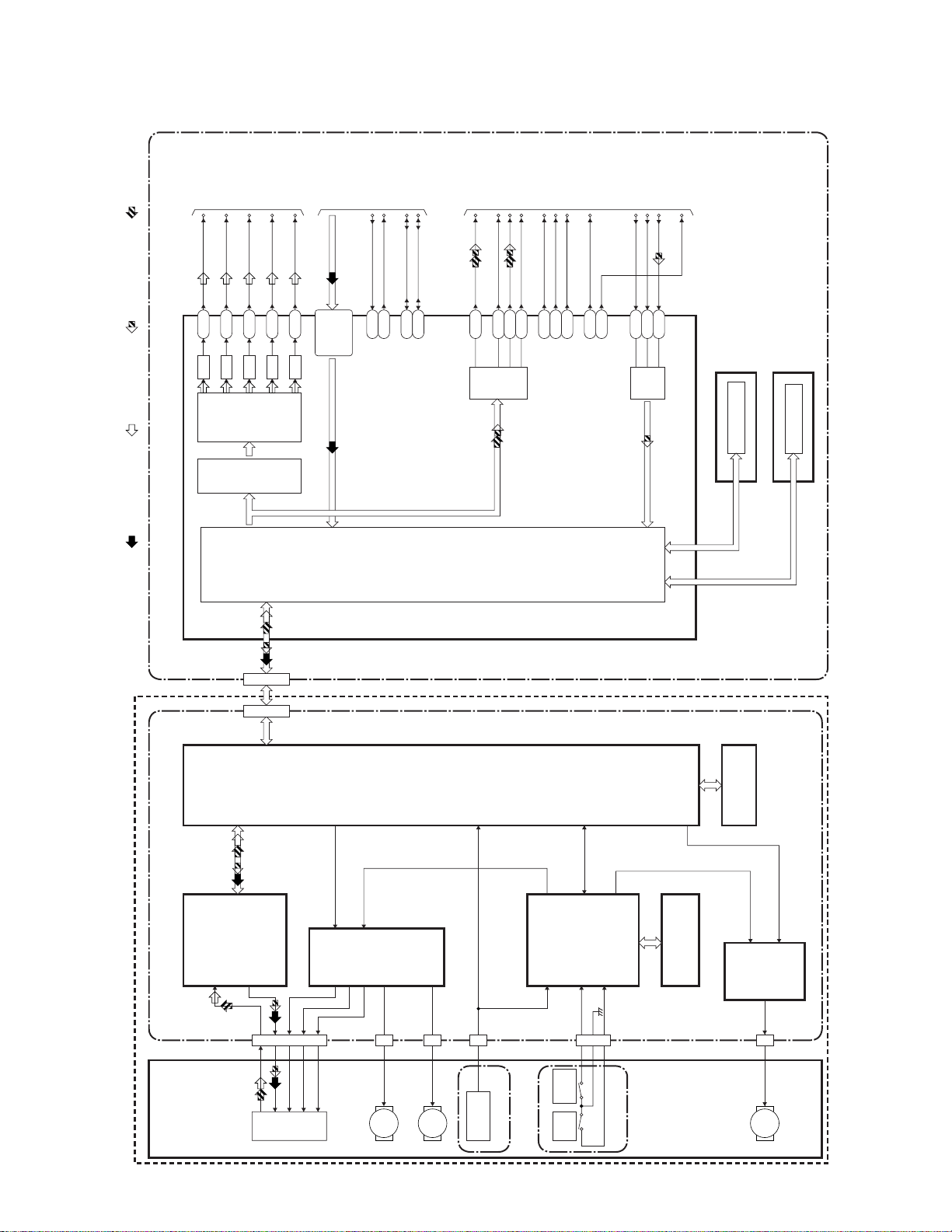
Digital Signal Process Block Diagram
TO VIDEO
INPUT SELECT
AD22,AF24
AC21,AB18,
BLOCK DIAGRAM
S-CLK
IC9-RESET
E25
AD21
S-CLK
IC9-RESET
SCL
Y4
SCL
SDA
AD2
SDA
SPDIF
VIDEO-Y(I)
AC12
Y(I)
D/A
TO VIDEO
OUTPUT SELECT
VIDEO-C
VIDEO-Y(I/P)
AE12
AC13
Y
C
D/A
D/A
VIDEO
ENCODER
BLOCK DIAGRAM
VIDEO-Cb
AD12
Cb
D/A
VIDEO-Cr
AE13
Cr
D/A
VID(0-7)
AC19,AE22,
AE23,AC20,
AB23
BCK
AUDIO
DATA
AD25
I/F
AC25
LRCK
AB22
MD
H24
MD
MC
J22
MC
ML
J23
ML
TO AUDIO
INPUT/OUTPUT
SELECT
BLOCK DIAGRAM
SCK
AB19
AC23
SCK
SYSCLK
LRCK
AB20
BCK
AB21
AUDIO
DATA
SYSCLK
DVD BE MAIN CBA UNITDVD FE MAIN CBA UNIT
AD24
I/F
FLASH MEMORY
DDR SDRAM
REC VIDEO SIGNAL PB VIDEO SIGNAL REC AUDIO SIGNAL PB AUDIO SIGNAL
IC3 (MAIN MICRO CONTRLLER)IC5301
VIDEO
I/F
CN1CN5301
BACK-END
DIGITAL
SIGNAL
FRONT-END
PROCESS
DIGITAL
SIGNAL
PROCESS
IC6 (FLASH MEMORY)
IC5401
IC1,IC2 (DDR SDRAM)
SDRAM
DVD MECHA
DVD MECHA & FE ASSEMBLY
IC5202
RF/
ERROR AMP
CN5101
TILT
PICK
IC5501
TRACKING
-UP
FOCUS
MOTOR
DRIVER
CN5603B
SLED
MOTOR
M
CN5502B
LOADING
MOTOR
FLASH
MEMORY
FRONT-END
MICRO
CN5602B
TRAY
CLOSE
TRAY
OPEN
CONTROLLER
LOADER CBA
IC5704
IC5503
MOTOR
CN5501
SPINDLE
MOTOR
DRIVER
M
E9410BLD
IC5703
CN5603
M
FE
ENCODER
ENCODER CBA
1-1-1
Page 4
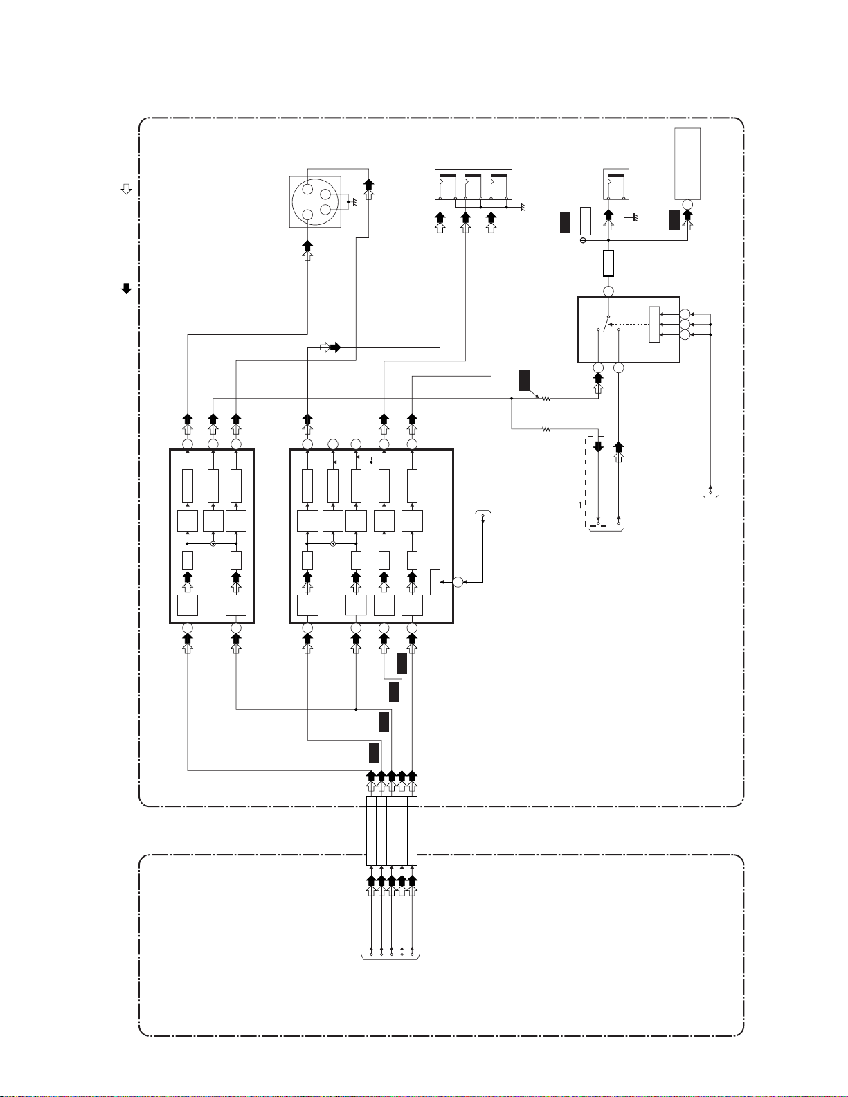
Video Output Select Block Diagram
JK1401
S-VIDEO
OUT
VIDEO-Y
OUT
VIDEO-Cb
OUT
VIDEO-Cr
OUT
COMPOSITE
VIDEO OUT
REC VIDEO SIGNAL PB VIDEO SIGNAL
IC1404 (VIDEO DRIVER)
5
2dB
AMP
LPF DRIVER
4dB
AMP
3
6
DRIVER
8dB
AMP
-6dB
7
2dB
AMP
LPF DRIVER
4dB
AMP
1
2
1
3 4
YC
15
14
13
DRIVER
2dB
AMP
8dB
AMP
2dB
AMP
-6dB
LPF DRIVER
4dB
AMP
IC1405 (VIDEO DRIVER)
3
LPF DRIVER
4dB
AMP
1
11
2dB
AMP
LPF DRIVER
4dB
AMP
6
10
DRIVER
2dB
AMP
LPF
4dB
AMP
8
JK1403
MUTE
TO SUB SYSTEM
V-MUTE
5
CONTROL
BLOCK DIAGRAM
WF6
WF1
IC1406
R1402
R1410
(OUTPUT SELECT)
JK751
TP751
V-OUT
BUFFER
Q391
2151
DVD-VIDEO(DUB)
PB/EE-VIDEO
(DVD VCR DUBBING)
TO VIDEO
BLOCK DIAGRAM
VIDEO-IN
TU900 (TUNER UNIT)
6
WF12
109 11
SW CTL
OUTPUT-SELECT
TO SERVO/SYSTEM CONTROL
BLOCK DIAGRAM
WF4
CN201
11VIDEO-Y(I)
CN7
VIDEO-Y(I/P)
VIDEO-Y(I)
WF8
WF7
WF5
14
VIDEO-Y(I/P)
14
16 16VIDEO-C
12 12VIDEO-Cb
10 10VIDEO-Cr
VIDEO-C
VIDEO-Cb
VIDEO-Cr
TO DIGITAL SIGNAL
PROCESS BLOCK
DIAGRAM
1-1-2
DVD BE MAIN CBA UNIT MAIN CBA
E9410BLVOS
Page 5

SCHEMATIC DIAGRAMS / CBA’S AND TEST POINTS
Standard Notes
WARNING
Many electrical and m echanical parts in this chassis
have special characteristics. These characteristics
often pass unnoticed and the protection afforded by
them cannot necessarily be obtained by using replacement components rated for higher voltage, wattage,
etc. Replacement par ts that have these specia l safety
characteristics are identified in this manual and its
supplements; electr ical components having such features are identified by the mark " # " in the schematic
diagram and the parts list. Before replacing any of
these components, read the par ts list in this manual
carefully. The use of substi tute replac ement par t s that
do not have the same safety characteristics as specified in the parts list may create shock, fire, or other
hazards.
Notes:
1. Do not use the part number shown on these drawings for ordering. The correct part number is shown
in the parts list, and may be slightly different or
amended since these drawings were prepared.
2. All resistance values are indicated in ohms
3
(K=10
3. Resistor wattages are 1/4W or 1/6W unl ess otherwise specified.
4. All capacitance values are indicated in µF
(P=10
5. All voltages are DC voltages unless otherwise
specified.
, M=106).
-6
µF).
1-2-1 W1-SC
Page 6

LIST OF CAUTION, NOTE S, AND SYMBOLS USED IN THE SCHEMATIC DIAGRAMS ON THE FOLLOWING
PAGES:
1. CAUTION:
FOR CONTINUED PROTECTION AGAINST FIRE HAZARD, REPLACE ONLY WITH THE SAME
F
A V
TYPE FUSE.
ATTENTION: POUR UNE PROTECTION CONTINUE LES RISQES D'INCELE N'UTILISER QUE
DES FUSIBLE DE MEMO TYPE.
RISK OF FIRE-REPLACE FUSE AS MARKED.
This symbol means fast operating fuse.
Ce symbole represente un fusible a fusion rapide.
2. CAUTION:
Fixed Voltage (or Auto voltage selectable) power supply circuit is used in this unit.
If Main Fuse (F1001) is blown, first check to see that all components in the power supply circuit are not defective
before you connect the AC plug to the AC power supply. O therwise it may cause some components in the
power supply circuit to fail.
3. Note:
(1) Do not use the part number shown on the drawings for ordering. The correct part number is shown in the parts
list, and may be slightly different or amended since the drawings were prepared.
(2) To maintain original function and reliability of repaired units, use only original replacement par ts which are
listed with their part numbers in the parts list section of the service manual.
4. Mode: SP/REC
5. Voltage indications for PLAY and REC modes on the schematics are as shown below:
< DVD Section >
5.0
The same voltage for
both PLAY & STOP modes
5.0
(2.5)
PLAY mode
STOP mode
231
Indicates that the voltage
is not consistent here.
The same voltage for
both PLAY, REC & DVD
modes
< VCR Section >
231
5.0
5.0
(2.5)
< >
Indicates that the voltage
is not consistent here.
PLAY mode
REC mode
DVD mode
6. How to read converged lines
1-D3
Distinction Area
3
AREA D3
Line Number
(1 to 3 digits)
2
AREA B1
Examples:
1. "1-D3" means that line number "1" goes to area "D3".
1
1-D3
2. "1-B1" means that line number "1" goes to area "B1".
ABCD
7. Test Point Information
: Indicates a test point with a jumper wire across a hole in the PCB.
: Used to indicate a test point with a component lead on foil side.
Unit: Volts
1-B1
: Used to indicate a test point with no test pin.
: Used to indicate a test point with a test pin.
1-2-2 SC_09
Page 7

Main 3/8 Schematic Diagram < VCR Section >
MAIN 3/8
Ref No. P os ition
IC301 O-2
Q301 Q-3
Q302 Q-4
Q303 Q-4
Q421 N-1
Q422 N-1
Q425 N-1
Q426 N-1
CN253 M-4
TP301 P-1
TP302 O-4
CONNECTOR
TEST PO I NTS
IC
TRANSISTORS
REC VIDEO SIGNAL
REC AUDIO SIGNAL
PB VIDEO SIGNAL
PB AUDIO SIGNAL
M4
M3
N4
N3
O4 P4 Q4 R4
O3
P3
Q3
R3
M2
M1
N2
N1
1-2-3
O2
O1
P2
P1
Q2
Q1
1-2-4
R2
R1
E9410SCM3
Page 8

Main 6/8 Schematic Diagram < VCR Section >
MAIN 6/8
Ref No. Pos ition
IC800 EE-2
IC801 GG-2
IC802 GG-1
IC803 HH-1
IC805 EE-3
IC900 FF-3
Q200 GG-1
Q201 GG-1
Q800 FF-2
Q801 FF-3
CN201 II-2
CN1609 DD-1
CONNECTORS
TRANSISTORS
ICS
REC VIDEO SIGNAL
REC AUDIO SIGNAL
PB VIDEO SIGNAL
PB AUDIO SIGNAL
DD4
DD3
EE4
EE3
FF4 GG4 HH4
FF3
GG3
HH3
II4
II3
DD2
DD1
1-2-5
EE2
EE1
FF2
FF1
GG2
GG1
HH2
HH1
II2
II1
1-2-6 E9410SCM6
Page 9

Main 7/8 Schematic Diagram < VCR Section >
MAIN 7/8
Ref No. Pos ition
IC804 KK-1
IC1404 LL-4
IC1405 LL-4
IC1406 LL-2
Q391 MM-2
Q802 JJ-2
Q804 LL-1
Q805 LL-1
Q806 LL-1
Q1351 MM-1
TP751 OO-4
TP753 NN-4
TP754 NN-4
TEST PO I NTS
TRANSISTORS
ICS
REC VIDEO SIGNAL
REC AUDIO SIGNAL
REC Audio Signal (Digital)
PB VIDEO SIGNAL
PB AUDIO SIGNAL
PB Audio Signal (Digital)
JJ4
JJ3
KK4
KK3
LL4 MM4 NN4
LL3
MM3
NN3
OO4
OO3
JJ2
JJ1
KK2
KK1
1-2-7 1-2-8
LL2
LL1
MM2
MM1
NN2
NN1
OO2
OO1
E9410SCM7
Page 10

Power Supply Schematic Diagram < VCR Section >
POWER SUPPLY
Ref No. Pos ition
IC010 C-1
Q031 D-1
Q1001 C-3
Q1003 B-3
Q1008 B-2
CN1607 E-4
CN1610 E-3
CONNECTORS
IC
TRANSISTORS
CAUTION !
Fixed voltage ( or Auto voltage selectable ) power supply circuit is used in this unit.
If Main Fuse (F1001) is blown, check to see that all components in the power supply
circuit are not defective before you connect the AC plug to the AC power supply.
Otherwise it may cause some components in the power supply circuit to fail.
F
A V
CAUTION
FOR CONTINUED PROTECTION AGAINST FIRE HAZARD,
REPLACE ONLY WITH THE SAME TYPE FUSE.
ATTENTION : POUR UNE PROTECTION CONTINUE LES RISQES
D'INCELE N'UTILISER QUE DES FUSIBLE DE MÊME TYPE.
RISK OF FIRE-REPLACE FUSE AS MARKED.
"This symbol means fast operating fuse."
"Ce symbole reprèsente un fusible à fusion rapide."
NOTE :
The voltage for parts in hot circuit is measured using
hot GND as a common terminal.
A4
A3
B4
B3
C4
C3
D4
D3
E4
E3
F4
F3
A2
A1
1-2-9
B2
B1
C2
C1
D2
D1
E2
E1
F2
F1
1-2-10 E9410SCP
Page 11

DVD BE Main 1/4 Schematic Diagram < DVD Section >
DVD B E M AI N 1 /4
Ref No. Pos i ti on
IC3(1/6) D-3
IC9 B-4
IC12 B-2
IC13 D-1
IC17 C-4
Q16 D-4
Q17 D-4
Q18 E-4
Q19 B-4
Q20 A-4
Q21 E-2
CN7
F-4
ICS
CONNECTOR
TRANSI S TORS
Note:
1. The order of pins shown are different from that of IC3 itself.
2. IC3 is shown as IC3(1/6) through IC3(6/6) in DVD BE Main Schematic Diagram section.
REC Video+Audio Signal (Digital)
REC Video Signal (Digital)
REC Video Signal
REC Audio Signal (Digital)
REC Audio Signal
PB Video+Audio Signal (Digital)
PB Video Signal (Digital)
PB Video Signal
PB Audio Signal (Digital)
PB Audio Signal
A4
A3
B4
B3
C4
C3
D4
D3
E4
E3
F4
F3
A2
A1
B2
B1
1-2-11 1-2-12
C2
C1
D2
D1
E2
E1
F2
F1
E9410SCBM1
Page 12

DVD BE Main 2/4 Schematic Diagram < DVD Section >
DVD B E M AI N 2 /4
Ref No. Pos i ti on
IC3(2/6) G-3
IC3(3/6) J-3
IC7 I-2
CN3
L-4
ICS
CONNECTOR
Note:
1. The order of pins shown are different from that of IC3 itself.
2. IC3 is shown as IC3(1/6) through IC3(6/6) in DVD BE Main Schematic Diagram section.
G4
G3
H4
H3
I4
I3
J4
J3
K4
K3
L4
L3
G2
G1
1-2-13
H2
H1
I2
I1
J2
J1
K2
K1
L2
L1
1-2-14 E9410SCBM2
Page 13

WIRING DIAGRAM < VCR SECTION >
(
>
TO WIRING
DIAGRAM
TO DVD
BE MAIN
CBA UNIT
CN6
(W02)
1
2
3
<DVD SECTION
9
6
8
TO DVD
BE MAIN
CBA UNIT
CN7
9
12
10
10
(W01)
16
15
16
19
27
TO DVD FE
MAIN CBA
UNIT CN5801
(W005)
2GND
3GND
4P-ON+5V
28
1P-ON+10V
29
30
REAR
ANT-IN ANT-OUT
DIGITAL
AUDIO
AUDIO-L
OUT1
AUDIO-R
OUT1
VIDEO-
Cr OUT
VIDEO-
Cb OUT
VIDEO-Y
OUT
AUDIO-R
IN1
AUDIO-L
IN1
VIDEO
IN1
AUDIO-R
OUT2
AUDIO-L
OUT2
VIDEO
OUT
S-VIDEO
OUT
OUT
CN202
VI+2.5V 1
VI+2.5V 2
VI+2.5V 4
GND 5
P-ON+2.5V 6
P-ON+2.5V 7
RW-SDA
RW-SCLK
2
3
P-ON+2.5V 8
RW-VPP5RW-RESET
RW-BUSY
4
VI+2.5V 3
RW-OEX
1
CN200 (NO CONNECTION)
MAIN CBA
(BE9400F01011A)
GND 9
P-ON+3.3V 10
P-ON+3.3V 11
GND
BUP+5V
6
7
8
P-ON+3.3V 12
GND 13
GND 14
P-ON+5V 15
GND 16
GND 17
NO PART MOUNTED
FOR CN200
SPDIF 18
CN201
VIDEO-Y(I)
CN1608
CN1609
CN1608
CN1607
GND
SUB-SCLK
FID
SUB-TXD
RDY4SUB-RXD5SYS-RESET
GND13
AL+5V14
DVD+5V15
AL+12V(1)17
AL+12V(2)
AL+44V18
16
12467
33
5
1234567
23457
1
AL+44V
6
GND
GND
AL+5V
AL+12V
P-DOWN-L
SENSOR CBA
(BHB300F01014A,B)
VIDEO-Cb
GND
GND7VIDEO-Cr
NU
AL-30V9
GND10
GND12
GND11
8
9
8
101113
9
8
1234567
CN1611
9
8
1
NU
NU
CN1610
AL-24V
AL+2.35V
SENSOR CBA
(BHB300F01014A,B)
GND11VIDEO-Y(I/P)
AL+2.5V7
12
23457
GND
CN1616
W002
CN1615
Y-IN1
GND13VIDEO-C14GND
GND17C-IN118DVD-A-MUTE
GND5
EV+5V
F2
AL+3.3V4
GND6
F13
2
1
161718
14
15
8
9
9
8
6
F2
F2
F1
F2
GND
GND
AL+4V
FUNCTION CBA
(BH9600F01011C)
DVD-KEY-2
DVD-KEY-1
22
11
CN1614
W001
GND
33
CN1613
CN1605
1
W011
C-IN2
1
CN1609
AUDIO+5V
FAN
JACK CBA
2
3
Y-IN2
SDET-2(NU)
2
3
GND20AUDIO(R)21GND22AUDIO(L)23GND24A-OUT(L)25GND26A-OUT(R)
JUNCTION CBA
(BH9400F01021B)
POWER SUPPLY
CBA
(BH9400F01021A)
POWER SW CBA
(BH9400F01011B)
POWER-LED
POWER-KEY
GND
11
22
3 3
CN1604
CN1606
FAN+9.5V
GND
1
2
AC CORD
(BH9400F01011D)
5
8
4
6
7
GND
A(R)-IN2
V-IN2
A(L)-IN2
GND
5
8
4
6
7
S-VIDEO
FRONT
OUT
AUDIO
IN (L)
AUDIO
IN (R)
VIDEO
IN
S-VIDEO
IN
CN504
AE-H
1
AE-H/FE-H
A-COM
A-PB/REC
CTL(+)
23456
CTL(-)
FE-H
CN501
1
FE-H GND
2
CN502
CAPSTAN
MOTOR
C-FG
AL+12V(1)
P-ON+5V
1
23456
M
C-F/R
C-CONT
GND
CAPSTAN
MOTOR
GND
D-CONT
D-PFG
LM-FWD/REV
8
9
7
101112
AL+18V
AL+12V
CN253
V(L)-2
V(L)-1
V(R)-1
V-COM
1234567
V-COM
V(R)-2
Hi-Fi-A(R)
Hi-Fi-COM
Hi-Fi-A(L)
8
9
M
SENSOR
M
DRUM
MOTOR
VIDEO
(R)1
HEAD
VIDEO
(L)1
HEAD
VIDEO
(L)2
HEAD
VIDEO
(R)2
HEAD
Hi-Fi
AUDIO
(R) HEAD
Hi-Fi
AUDIO
(L) HEAD
E9410WI
PG
CYLINDER
AUDIO
AC HEAD
ASSEMBLY
DECK ASSEMBLY)
HEAD
ERASE
HEAD
AUDIO
HEAD
CONTROL
FE HEAD
FULL
ERASE
HEAD
LOADING
MOTOR
ASSEMBLY
1-3-1
Page 14
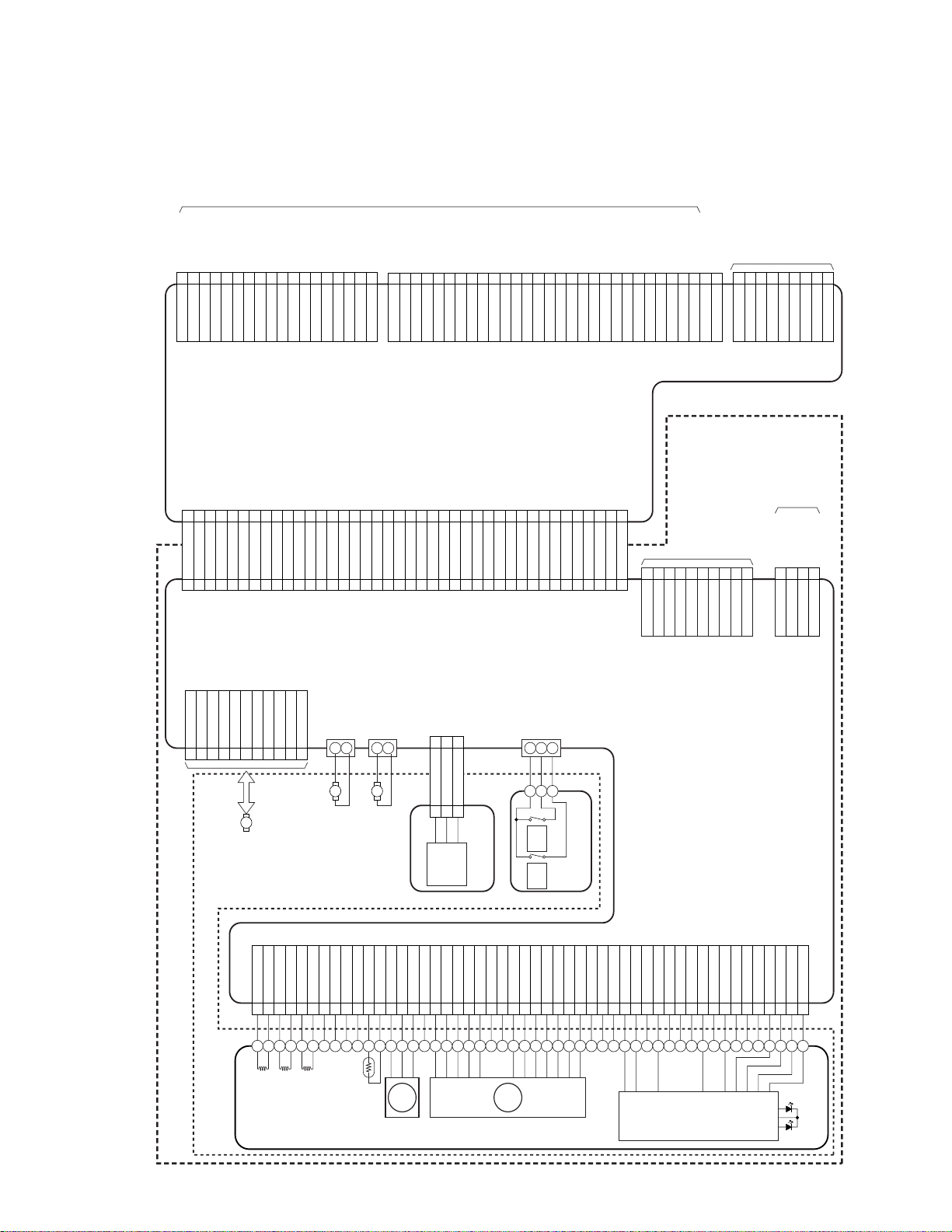
WIRING DIAGRAM < DVD SECTION >
>
TO WIRING
DIAGRAM
<VCR SECTION
CN6
CN5301 CN1
TO MAIN
CBA CN202
(W02)
VI+2.5V 1
VI+2.5V 2
VI+2.5V 4
GND 5
P-ON+2.5V 6
P-ON+2.5V 7
P-ON+2.5V 8
GND 9
P-ON+3.3V 10
P-ON+3.3V 11
P-ON+3.3V 12
GND 13
GND 14
P-ON+5V 15
VI+2.5V 3
GND 16
2
1
3
CN7
GND 17
SPDIF 18
VIDEO-Y(I)
GND
SUB-SCLK
FID
9
6
8
SUB-TXD
RDY4SUB-RXD5SYS-RESET
GND7VIDEO-Cr
9
10
10
GND
TO MAIN
CBA CN201
12
GND11VIDEO-Y(I/P)
VIDEO-Cb
(W01)
16
15
16
GND13VIDEO-C14GND
19
Y-IN1
GND17C-IN118DVD-A-MUTE
GND20AUDIO(R)21GND22AUDIO(L)23GND24A-OUT(L)25GND26A-OUT(R)
28
29
27
30
CN3
AUDIO+5V
(NO CONNECTION)
1
TMODE02JTDI3JTRST4JTMS5P-ON+3.3V6JTDO7GND8JTCK9SYS-RESET
DVD BE MAIN CBA UNIT
TO WIRING
DIAGRAM
<VCR SECTION>
2525
2222
(NO CONNECTION)
1P-ON+5V(4)
2RXD
3TXD
4SCK1
5/RST-S
6JL-CLK
7GND
8P-ON+3.3V(2)
GND
IORB
DIORB 2323
GND 2424
GND 2626
ORDY 2727
GND 2828
DMACKB 2929
GND 3030
INTRQ 3131
NU 3232
DA1 3333
PDIAG(NU) 3434
DA0 3535
DA2 3636
CS0B 3737
CS1B 3838
DASP(NU) 3939
RESETB 11
GND 22
DD8 44
DD6 55
DD9 66
DD5 77
DD10 88
DD4 99
DD11 1010
DD3 1111
DD12 1212
DD2 1313
DD13 1414
DD1 1515
DD14 1616
DD0 1717
DD15 1818
GND 1919
NU 2020
DD7 33
DMARQB 2121
GND 4040
CN5701
9SCISEL0
10SCISEL1
1P-ON+10V
CN5801
TO MAIN
CBA CN1604
(W005)
3GND
2GND
4P-ON+5V
DVD MECHA & FE ASSEMBLY
CN5501
W
1
2V3U4
DVD MECHA
VCC5HU+6HU-7HV+8HV-9HW+
M
SPINDLE
MOTOR
FCS(+) 4TRK(-)
TRK(+)
CN5101
1
3
2 FCS(-)
FOCUS
ACTUATOR
TRACKING
PICKUP UNIT
HW-11VH10
ACTUATOR
5 TILT(+)
TILT
6 TILT(-)
ACTUATOR
CN5502B
M
LOADING
MOTOR
GND
7
8NU
9NU
CN5603B
SLED
THERMO
10 NU
11
M
MOTOR
GND
FPD14FPD-SW
12
13
FPDIC
CN5603
GND 11
T-SCN2 22
T-SCN3 33
FFC6001
SLED
SENSOR
VC-PD18H19A20B21F22NU23NU24SW25RF(+)26RF(-)27E28C29D30G31GND32VCC233NU34IIN435IIN336NU37IIN138GND39NU40NU41XOUTEN442GND43XOUTEN344GND45NU46NU47OSCMOD48OSCEN49LDEN250LDEN1
VCC1
VC-FPD
15
17
16
PDIC
CN5602B
TRAY
ENCODER CBA
TRAY
OUT
IN
LOADER CBA
DVD FE MAIN CBA UNIT
DVD/CD
LASER
DIODE
DRIVE
CD-LDDVD-LD
1-3-2
E9410WID
Page 15

Different parts from original model (EWR20V4)
Ref. No. Description Part No.
Mechanical Parts
A1X FRONT ASSEMBLY E9410UD 0VM204564
A10# LABEL, RATING(U) E9410UD or --------# LABEL, RATING(D) E9410UD --------A14 LABEL, BAR CODE HB400UD or ---------
LABEL, BAR CODE E9410UD --------A18 LABEL, TELEPHONE NUMBER H5730UD(SYLVANIA) --------A34 FOOT H5100UD 0VM406940
2B19 Not Used
S1 GIFT BOX CARTON E94 10UD 0VM306790
X20# OWNER'S MANUAL E9410UD 0VMN04183
X22 Not Used
Electrical Parts
DVD BE MAIN CBA UNIT N7814FUP
MCV CBA 1VSA10150
C1403 CHIP CERAMIC CAP.(1608) B K 0.33µF/10V CHD1AK30B334
C1423 CHIP CERAMIC CAP.(1608) B K 0.01µF/50V CHD1JK30B103
C1443 ELECTROLYTIC CAP. 470µF/6.3V M or CE0KMASDL471
ELECTROLYTIC CAP. 470µF/6.3V M CE0KMASTL471
C1535 CHIP CERAMIC CAP.(1608) B K 0.01µF/50V CHD1JK30B103
C1536 ELECTROLYTIC CAP. 22µF/6.3V M H7 CE0KMAVSL220
C1537 CHIP CERAMIC CAP.(1608) F Z 0.1µF/25V CHD1EZ30F104
CN201 FMN CONNECTOR, TOP 30P 30FMN-BTRK JCFNG30JG002
D012 SCHOTTKY BARRIER DIODE SB390 or NDQZ000SB390
SCHOTTKY BARRIER DIODE SB360 NDQZ000SB360
IC1404 DRIVER FOR DVD MM1636XWRE QSZBA0TMM108
W01 Not Used
W04 FFC CABLE 30P FFC/P1.00/170 WX1E9400-014
1-4-1 E9410PL
Page 16

DVR90VE
E9410UD
2004-04-23
 Loading...