

Page 1

SERVICE MANUAL
DVD RECORDER
DVR900E
Page 2

IMPORTANT SAFETY NOTICE
Proper service and repair is important to the safe, reliable operation of all
Funai Equipment. The service procedures recommended by Funai and
described in this service manual are effective methods of performing
service operations. Some of these service special tools should be used
when and as recommended.
It is important to note that this service manual contains various CAUTIONS
and NOTICES which should be carefully read in order to minimize the risk of
personal injury to service personnel. The possibility exists that improper
service methods may damage the equipment. It also is important to
understand that these CAUTIONS and NOTICES ARE NOT EXHAUSTIVE.
Funai could not possibly know, evaluate and advice the service trade of all
conceivable ways in which service might be done or of the possible
hazardous consequences of each way. Consequently, Funai has not
undertaken any such broad evaluation. Accordingly, a servicer who uses a
service procedure or tool which is not recommended by Funai must first
use all precautions thoroughly so that neither his safety nor the safe
operation of the equipment will be jeopardized by the service method
selected.
TABLE OF CONTENTS
SPECIFICATIONS . . . . . . . . . . . . . . . . . . . . . . . . . . . . . . . . . . . . . . . . . . . . . . . . . . . . . . . . . . . . . . . . . . . . . . 1-1-1
LASER BEAM SAFETY PRECAUTIONS . . . . . . . . . . . . . . . . . . . . . . . . . . . . . . . . . . . . . . . . . . . . . . . . . . . . 1-2-1
IMPORTANT SAFETY PRECAUTIONS . . . . . . . . . . . . . . . . . . . . . . . . . . . . . . . . . . . . . . . . . . . . . . . . . . . . . 1-3-1
STANDARD NOTES FOR SERVICING . . . . . . . . . . . . . . . . . . . . . . . . . . . . . . . . . . . . . . . . . . . . . . . . . . . . . 1-4-1
OPERATING CONTROLS AND FUNCTIONS . . . . . . . . . . . . . . . . . . . . . . . . . . . . . . . . . . . . . . . . . . . . . . . . 1-5-1
CABINET DISASSEMBLY INSTRUCTIONS . . . . . . . . . . . . . . . . . . . . . . . . . . . . . . . . . . . . . . . . . . . . . . . . . . 1-6-1
HOW TO INITIALIZE THE DVD RECORDER . . . . . . . . . . . . . . . . . . . . . . . . . . . . . . . . . . . . . . . . . . . . . . . . . 1-6-4
BLOCK DIAGRAMS. . . . . . . . . . . . . . . . . . . . . . . . . . . . . . . . . . . . . . . . . . . . . . . . . . . . . . . . . . . . . . . . . . . . . 1-7-1
FUNCTION INDICATOR SYMBOLS . . . . . . . . . . . . . . . . . . . . . . . . . . . . . . . . . . . . . . . . . . . . . . . . . . . . . . . . 1-7-6
SCHEMATIC DIAGRAMS / CBA’S AND TEST POINTS . . . . . . . . . . . . . . . . . . . . . . . . . . . . . . . . . . . . . . . . . 1-8-1
WAVEFORMS . . . . . . . . . . . . . . . . . . . . . . . . . . . . . . . . . . . . . . . . . . . . . . . . . . . . . . . . . . . . . . . . . . . . . . . . . 1-9-1
WIRING DIAGRAM . . . . . . . . . . . . . . . . . . . . . . . . . . . . . . . . . . . . . . . . . . . . . . . . . . . . . . . . . . . . . . . . . . . . 1-10-1
FIRMWARE RENEWAL MODE . . . . . . . . . . . . . . . . . . . . . . . . . . . . . . . . . . . . . . . . . . . . . . . . . . . . . . . . . . . 1-11-1
SYSTEM CONTROL TIMING CHARTS . . . . . . . . . . . . . . . . . . . . . . . . . . . . . . . . . . . . . . . . . . . . . . . . . . . . 1-12-1
IC PIN FUNCTION DESCRIPTIONS. . . . . . . . . . . . . . . . . . . . . . . . . . . . . . . . . . . . . . . . . . . . . . . . . . . . . . . 1-13-1
LEAD IDENTIFICATIONS . . . . . . . . . . . . . . . . . . . . . . . . . . . . . . . . . . . . . . . . . . . . . . . . . . . . . . . . . . . . . . . 1-14-1
EXPLODED VIEWS . . . . . . . . . . . . . . . . . . . . . . . . . . . . . . . . . . . . . . . . . . . . . . . . . . . . . . . . . . . . . . . . . . . . 1-15-1
MECHANICAL PARTS LIST . . . . . . . . . . . . . . . . . . . . . . . . . . . . . . . . . . . . . . . . . . . . . . . . . . . . . . . . . . . . . 1-16-1
ELECTRICAL PARTS LIST . . . . . . . . . . . . . . . . . . . . . . . . . . . . . . . . . . . . . . . . . . . . . . . . . . . . . . . . . . . . . . 1-17-1
Manufactured under license from Dolby Laboratories. "Dolby"
and the double-D symbol are trademarks of Dolby Laboratories.
Page 3

SPECIFICATIONS
ITEM CONDITIONS UNIT NOMINAL LIMIT
1. VIDEO
1-1. Video Output 75 ohm load Vp-p 1.0
1-2. S-Video Output
Y (Luminance) 75 ohm load Vp-p 1.0
C (Chrominance) 75 ohm load Vp-p 0.286
1-3. Component Output
Y (Luminance) 75 ohm load Vp-p 1.0
Cb (Chrominance) 75 ohm load Vp-p 0.7
Cr (Chrominance) 75 ohm load Vp-p 0.7
2. AUDIO
2-1. Output Level Vrms 2.0
2-2. Frequency Response
DVD-VIDEO LPCM fs = 96 kHz kHz 0.004 - 44
fs = 48 kHz kHz 0.004 - 22
Audio CD fs = 44.1 kHz kHz 0.004 - 20
2-3. Signal/Noise Ratio
DVD-VIDEO LPCM dB 120
CD dB 120
REC & Playback Input: 2 Vrms, Rec Speed: XP dB 93
2-4. Dynamic Range
DVD-VIDEO LPCM dB 100
CD dB 98
REC & Playback Input: 2 Vrms, Rec Speed: XP dB 92
2-5. THD+N 1 kHz, 0 dB
DVD-VIDEO LPCM % 0.004
CD % 0.004
REC & Playback Input: 2 Vrms, Rec Speed: XP % 0.006
NOTES:
1. All Items are measured without pre-emphasis unless otherwise specified.
2. Power supply : AC120 V 60 Hz
3. Load imp. : 100 k ohm
4. Room ambient : 5
°C ~ 40 °C
1-1-1 E6500SP
Page 4

LASER BEAM SAFETY PRECAUTIONS
This DVD player uses a pickup that emits a laser beam.
Do not look directly at the laser beam coming
from the pickup or allow it to strike against
your skin.
The laser beam is emitted from the location shown in the figure. When checking the laser diode, be sure to keep
your eyes at least 30cm away from the pickup lens when the diode is turned on. Do not look directly at the laser
beam.
Caution: Use of controls and adjustments, or doing procedures other than those specified herein, may result in
hazardous radiation exposure.
Drive Mecha Assembly
Laser Beam Radiation
Laser Pickup
Turntable
Location: Inside Top of DVD mechanism.
1-2-1 E6_LASER
Page 5

IMPORTANT SAFETY PRECAUTIONS
Product Safety Notice
Some electrical and mechanical parts have special
safety-related characteristics which are often not evident from visual inspection, nor can the protection
they give necessarily be obtained by replacing them
with components rated for higher voltage, wattage,
etc. Parts that have special safety characteristics are
identified by a # on schematics and in parts lists. Use
of a substitute replacement that does not have the
same safety characteristics as the recommended
replacement part might create shock, fire, and/or other
hazards. The Product’s Safety is under review continuously and new instructions are issued whenever
appropriate. Prior to shipment from the factory, our
products are carefully inspected to confirm with the
recognized product safety and electrical codes of the
countries in which they are to be sold. However, in
order to maintain such compliance, it is equally important to implement the following precautions when a set
is being serviced.
Precautions during Servicing
A. Parts identified by the # symbol are critical for
safety. Replace only with part number specified.
B. In addition to safety, other parts and assemblies
are specified for conformance with regulations
applying to spurious radiation. These must also be
replaced only with specified replacements.
Examples: RF converters, RF cables, noise blocking capacitors, and noise blocking filters, etc.
C. Use specified internal wiring. Note especially:
1)Wires covered with PVC tubing
2)Double insulated wires
3)High voltage leads
D. Use specified insulating materials for hazardous
live parts. Note especially:
1)Insulation tape
2)PVC tubing
3)Spacers
4)Insulators for transistors
E. When replacing AC primary side components
(transformers, power cord, etc.), wrap ends of
wires securely about the terminals before soldering.
F. Observe that the wires do not contact heat produc-
ing parts (heatsinks, oxide metal film resistors, fusible resistors, etc.).
G. Check that replaced wires do not contact sharp
edges or pointed parts.
H. When a power cord has been replaced, check that
5 - 6 kg of force in any direction will not loosen it.
I. Also check areas surrounding repaired locations.
J. Be careful that foreign objects (screws, solder
droplets, etc.) do not remain inside the set.
K. Crimp type wire connector
The power transformer uses crimp type connectors
which connect the power cord and the primary side
of the transformer. When replacing the transformer,
follow these steps carefully and precisely to prevent shock hazards.
Replacement procedure
1)Remove the old connector by cutting the wires at a
point close to the connector.
Important: Do not re-use a connector. (Discard it.)
2)Strip about 15 mm of the insulation from the ends
of the wires. If the wires are stranded, twist the
strands to avoid frayed conductors.
3)Align the lengths of the wires to be connected.
Insert the wires fully into the connector.
4)Use a crimping tool to crimp the metal sleeve at its
center. Be sure to crimp fully to the complete closure of the tool.
L. When connecting or disconnecting the internal con-
nectors, first, disconnect the AC plug from the AC
outlet.
1-3-1 DVD_SFN1
Page 6

Safety Check after Servicing
Examine the area surrounding the repaired location for
damage or deterioration. Observe that screws, parts,
and wires have been returned to their original positions. Afterwards, do the following tests and confirm
the specified values to verify compliance with safety
standards.
1. Clearance Distance
When replacing primary circuit components, confirm
specified clearance distance (d) and (d’) between soldered terminals, and between terminals and surrounding metallic parts. (See Fig. 1)
Table 1: Ratings for selected area
AC Line Voltage Clearance Distance (d), (d’)
Chassis or Secondary Conductor
Primary Circuit Terminals
dd'
120 V
Note: This table is unofficial and for reference only.
Be sure to confirm the precise values.
2. Leakage Current Test
Confirm the specified (or lower) leakage current
between B (earth ground, power cord plug prongs)
and externally exposed accessible parts (RF terminals, antenna terminals, video and audio input and
output terminals, microphone jacks, earphone jacks,
etc.) is lower than or equal to the specified value in the
table below.
Measuring Method (Power ON) :
Insert load Z between B (earth ground, power cord
plug prongs) and exposed accessible parts. Use an
AC voltmeter to measure across the terminals of load
Z. See Fig. 2 and the following table.
Table 2: Leakage current ratings for selected areas
AC Line Voltage Load Z Leakage Current (i) Earth Ground (B) to:
120 V
≥ 3.2mm (0.126 inches)
0.15µF CAP. & 1.5kΩ RES.
Connected in parallel
Exposed Accessible Part
Z
1.5k
i≤0.5mA Peak Exposed accessible parts
0.15 F
Earth Ground
B
Power Cord Plug Prongs
AC Voltmeter
(High Impedance)
Fig. 1
Fig. 2
Note: This table is unofficial and for reference only. Be sure to confirm the precise values.
1-3-2 DVD_SFN1
Page 7

STANDARD NOTES FOR SERVICING
Circuit Board Indications
1. The output pin of the 3 pin Regulator ICs is indicated as shown.
Top View
Out
2. For other ICs, pin 1 and every fifth pin are indicated
as shown.
Pin 1
3. The 1st pin of every male connector is indicated as
shown.
Input
In
Bottom View
5
10
Pb (Lead) Free Solder
When soldering, be sure to use the Pb free solder.
How to Remove / Install Flat Pack-IC
1. Removal
With Hot-Air Flat Pack-IC Desoldering Machine:.
(1) Prepare the hot-air flat pack-IC desoldering
machine, then apply hot air to the Flat Pack-IC
(about 5 to 6 seconds). (Fig. S-1-1)
Pin 1
Instructions for Connectors
1. When you connect or disconnect the FFC (Flexible
Foil Connector) cable, be sure to first disconnect
the AC cord.
2. FFC (Flexible Foil Connector) cable should be
inserted parallel into the connector, not at an angle.
FFC Cable
Connector
CBA
* Be careful to avoid a short circuit.
Fig. S-1-1
(2) Remove the flat pack-IC with tweezers while apply-
ing the hot air.
(3) Bottom of the flat pack-IC is fixed with glue to the
CBA; when removing entire flat pack-IC, first apply
soldering iron to center of the flat pack-IC and heat
up. Then remove (glue will be melted). (Fig. S-1-6)
(4) Release the flat pack-IC from the CBA using twee-
zers. (Fig. S-1-6)
Caution:
1. The Flat Pack-IC shape may differ by models. Use
an appropriate hot-air flat pack-IC desoldering
machine, whose shape matches that of the Flat
Pack-IC.
2. Do not supply hot air to the chip parts around the
flat pack-IC for over 6 seconds because damage to
the chip parts may occur. Put masking tape around
the flat pack-IC to protect other parts from damage.
(Fig. S-1-2)
1-4-1 E6STA
Page 8

3. The flat pack-IC on the CBA is affixed with glue, so
be careful not to break or damage the foil of each
pin or the solder lands under the IC when removing
it.
With Soldering Iron:
(1) Using desoldering braid, remove the solder from all
pins of the flat pack-IC. When you use solder flux
which is applied to all pins of the flat pack-IC, you
can remove it easily. (Fig. S-1-3)
CBA
Masking
Tape
Tweezers
Hot-air
Flat Pack-IC
Desoldering
Machine
Flat Pack-IC
Fig. S-1-2
Flat Pack-IC
Desoldering Braid
Soldering Iron
Fig. S-1-3
(2) Lift each lead of the flat pack-IC upward one by
one, using a sharp pin or wire to which solder will
not adhere (iron wire). When heating the pins, use
a fine tip soldering iron or a hot air desoldering
machine. (Fig. S-1-4)
Sharp
Pin
Fine Tip
Soldering Iron
(3) Bottom of the flat pack-IC is fixed with glue to the
CBA; when removing entire flat pack-IC, first apply
soldering iron to center of the flat pack-IC and heat
up. Then remove (glue will be melted). (Fig. S-1-6)
(4) Release the flat pack-IC from the CBA using twee-
zers. (Fig. S-1-6)
Fig. S-1-4
1-4-2 E6STA
Page 9

With Iron Wire:
(1) Using desoldering braid, remove the solder from all
pins of the flat pack-IC. When you use solder flux
which is applied to all pins of the flat pack-IC, you
can remove it easily. (Fig. S-1-3)
(2) Affix the wire to a workbench or solid mounting
point, as shown in Fig. S-1-5.
(3) While heating the pins using a fine tip soldering
iron or hot air blower, pull up the wire as the solder
melts so as to lift the IC leads from the CBA contact
pads as shown in Fig. S-1-5.
(4) Bottom of the flat pack-IC is fixed with glue to the
CBA; when removing entire flat pack-IC, first apply
soldering iron to center of the flat pack-IC and heat
up. Then remove (glue will be melted). (Fig. S-1-6)
(5) Release the flat pack-IC from the CBA using twee-
zers. (Fig. S-1-6)
Note:
When using a soldering iron, care must be taken
to ensure that the flat pack-IC is not being held by
glue. When the flat pack-IC is removed from the
CBA, handle it gently because it may be damaged
if force is applied.
Hot Air Blower
2. Installation
(1) Using desoldering braid, remove the solder from
the foil of each pin of the flat pack-IC on the CBA so
you can install a replacement flat pack-IC more
easily.
(2) The “I” mark on the flat pack-IC indicates pin 1.
(See Fig. S-1-7.) Be sure this mark matches the 1
on the PCB when positioning for installation. Then
presolder the four corners of the flat pack-IC. (See
Fig. S-1-8.)
(3) Solder all pins of the flat pack-IC. Be sure that none
of the pins have solder bridges.
Example :
Pin 1 of the Flat Pack-IC
is indicated by a " " mark.
Fig. S-1-7
To Solid
Mounting Point
CBA
Tweezers
Iron Wire
Soldering Iron
Fig. S-1-5
Fine Tip
Soldering Iron
Flat Pack-IC
or
Presolder
Flat Pack-IC
CBA
Fig. S-1-8
Fig. S-1-6
1-4-3 E6STA
Page 10

Instructions for Handling
Semi-conductors
Electrostatic breakdown of the semi-conductors may
occur due to a potential difference caused by electrostatic charge during unpacking or repair work.
1. Ground for Human Body
Be sure to wear a grounding band (1MΩ) that is properly grounded to remove any static electricity that may
be charged on the body.
2. Ground for Workbench
(1) Be sure to place a conductive sheet or copper plate
with proper grounding (1MΩ) on the workbench or
other surface, where the semi-conductors are to be
placed. Because the static electricity charge on
clothing will not escape through the body grounding band, be careful to avoid contacting semi-conductors with your clothing.
<Incorrect>
<Correct>
1MΩ
CBA
Grounding Band
1MΩ
CBA
Conductive Sheet or
Copper Plate
1-4-4 E6STA
Page 11

OPERATING CONTROLS AND FUNCTIONS
1-5-1 E6502IB
Page 12

1-5-2 E6502IB
Page 13

CABINET DISASSEMBLY INSTRUCTIONS
1. Disassembly Flowchart
This flowchart indicates the disassembly steps to gain
access to item(s) to be serviced. When reassembling,
follow the steps in reverse order. Bend, route, and
dress the cables as they were originally.
[1] Top Cover
[2] Front Assembly
[4] DVD Mecha & FE Assembly
[5] DVD BE Main CBA Unit
[6] Holder D
[8] AV CBA
[9] FL CBA
[10] Jack CBA
[3] SW CBA
[7] DC Fan Motor
2. Disassembly Method
(1): Identification (location) No. of parts in the figures
(2): Name of the part
(3): Figure Number for reference
(4): Identification of parts to be removed, unhooked,
unlocked, released, unplugged, unclamped, or
desoldered.
P=Spring, L=Locking Tab, S=Screw,
CN=Connector, W=Washer
*=Unhook, Unlock, Release, Unplug, or Desolder
e.g. 2(S-2) = two Screws (S-2),
2(L-2) = two Locking Tabs (L-2)
(5): Refer to “Reference Notes.”
Reference Notes
CAUTION 1: Be sure to remove the Top Cover with lifting up by the right and left portion in the front as
shown in Fig. D1.
CAUTION 2: Locking Tabs (L-1) and (L-2) are fragile.
Be careful not to break them.
2-1. Release four Locking Tabs (L-1). Then, release
three Locking Tabs (L-2).
2-2. Disconnect Connector (CN4203), and remove
the Front Assembly.
ID/
LOC.
No.
[1] Top Cover D1 6(S-1) 1
[2]
[3] SW CBA D2 3(S-2) -
[4]
[5]
[6] Holder D D4 3(S-6) -
[7]
[8] AV CBA D5 5(S-7), 7(S-8), (W-1) -
PART
Front
Assembly
DVD
Mecha &
FE
Assembly
DVD BE
Main CBA
Unit
DC Fan
Motor
Fig.
No.
D2
D3
D4
D4
REMOVAL
REMOVE/*UNHOOK/
UNLOCK/RELEASE/
UNPLUG/DESOLDER
*4(L-1), *3(L-2),
*CN4203
2(S-3), 4(S-4), *CN1,
*CN2202, Fan Sheet
4(S-5), *CN6, *CN7,
BE Earth Spring
2(S-7), *CN2203,
Fan Holder
Note
2
2-1
2-2
-
-
-
[1] Top Cover
(S-1)
(S-1)
(S-1)
Fig. D1
[9] FL CBA D5 (S-9), desolder -
[10] Jack CBA D5 (S-10), desolder -
↓
(1)
↓
(2)
↓
(3)
↓
(4)
↓
(5)
1-6-1 E6500DC
Page 14

[3] SW CBA
(S-2)
(L-1)
CN4203
[5] DVD BE Main CBA Unit
(S-5)
(S-6)
CN7
CN6
(S-5)
BE Earth Spring
(S-6)
Fan Holder
[7] DC Fan Motor
(L-2)
(S-2)
(L-1)
(L-1)
[2] Front Assembly
(S-3)
(S-4)
[6] Holder D
(S-7)
CN2203
Fig. D2
Fig. D4
Fan Sheet
(S-4)
[4] DVD Mecha
& FE Assembly
CN1
CN2202
Fig. D3
1-6-2 E6500DC
Page 15

[10] Jack CBA
(S-7)
(S-10)
(S-9)
(S-7)
(W-1)
(S-7)
[8] AV CBA
Lead with
red stripe
[9] FL CBA
Desolder
HOW TO EJECT MANUALLY
1. Remove the Top Cover.
2. Remove the Front Assembly.
3. Push the lever to the direction of the arrow as shown
below.
Lead with
red stripe
(S-8)
Desolder
Fig. D5
View for A
Push the lever to the
direction of the arrow
A
Lever
1-6-3 E6500DC
Page 16

HOW TO INITIALIZE THE DVD RECORDER
To put the program back at the factory-default, initialize
the DVD recorder as the following procedure.
1. Turn the DVD recorder on.
2. Confirm that no disc is loaded or that the disc tray
is open. To put the DVD recorder into the Version
display mode, press [CM SKIP], [1], [2], and [3] buttons on the remote control in the order.
Fig. A appears on the screen.
Model Name :
Firmware Version
BE : R1F189000E
FE : NRS0051 MST031210
DEFAULT SETTING : ENTER
EXIT : RETURN
*1: "
*2: Firmware Version differ depending on the models,
and indication is one example.
" differ depending on the models.
*******
*******
Fig. A: Version Display Mode Screen
3. Press [ENTER] button, then the DVD recorder
starts initializing. When the initializing is completed,
the DVD recorder exits the Version display mode
and turns off the power automatically.
* To move into the Normal mode from the Version
display mode, press [RETURN] button on the
remote control instead of [ENTER] button.
* When [POWER] button is pressed before [ENTER]
button is pressed, the DVD recorder exits the Version display mode, then the power turns off.
1-6-4 E6500DC
Page 17

BLOCK DIAGRAMS
System Control Block Diagram
TO POWER SUPPLY
POW-SW
REG-CONT
646125
POW-SW
REG-COUT
BLOCK DIAGRAM
PWSW
PWSW
FID
42
FID
TO VIDEO
V-MUTE
SUB-SDA
39
V-MUTE
BLOCK DIAGRAM
SUB-SCL
TO AUDIO
BLOCK DIAGRAM
A-MUTE
AUDIO-SW1
AUDIO-SW2
4745465453
A-MUTE
AUDIO-SW1
AUDIO-SW2
SUB-SCL
SUB-SDA
SUB-SDA
SUB-SCL
X4201
23
X OUT
8MHz
RESONATOR
22
X IN
X4202
32.768KHz
X'TAL
21
20
XC IN
XC OUT
Q4261
IC4202
EV+5V
RESET
4 5
19
RESET
16
P-DOWN
Q4262
C4261
57
VCC
(BACKUP CAPACITOR)
FIP
FL2301
GRID
~
23
~
1G
(FIP DRIVER)
DIN
CLK
IC2301
1
28
CN2301CN2204
FL-SDA 55FL-SCL 6
6
9
10
FL-SCL
FL-SDA
17
7G
STB
2
FL-STB 7
7
8
FL-STB
RE2301
8
REMOTE
8
4
REMOTE
SEGMENT
~
7
~
a
SENSOR
REMOTE
FL CBA
16
14
i
h
KEY SWITCH
KEY SWITCH
SW CBA
KEY-1 2
KEY-2 3
2
3
CN4203 CN3001
1
2
KEY-1
KEY-2
AV CBA
IC4201
(SUB MICRO CONTROLLER)
IC3
(MAIN MICRO CONTROLLER)
SUB-RXD
SYS-RESET
4052515041
CN4401
SYS-RESET 6
SUB-RXD 5
6
5
CN7
Q16
F24
D22
SUB-RXD
SYS-RESET
SUB-TXD
SUB-SCLK
RDY
SUB-TXD 3
RDY 4
SUB-SCLK 1
3
4
1
Q17
F25
H22
G22
RDY
SUB-TXD
SUB-SCLK
IC7
(INVERTER)
27MHz CLK
27MHz CLK
N23
R23
1 6
3
27MHz
X'TAL
4
X3
DVD BE MAIN CBA
1-7-1
E6502BLS
Page 18

Digital Signal Process Block Diagram
TO VIDEO
BLOCK DIAGRAM
SCL
SDA
VIDEO-Y
AE12
Y
D/A
VIDEO-C
AC13
C
D/A
VIDEO
ENCODER
VIDEO-Cr
VIDEO-Cb
AD12
Cr
Cb
D/A
AE13
D/A
VID(0-7)
AD22,AF24
AC19,AE22,
AE23,AC20,
AC21,AB18,
S-CLK
IC9-RESET
E25
AD21
S-CLK
IC9-RESET
Y4
SCL
AD2
SDA
SPDIF
AB23
BCK
AUDIO
DATA
AD25
I/F
AC25
LRCK
AB22
MD
H24
MD
MC
J22
MC
TO AUDIO
BLOCK DIAGRAM
ML
SCK
LRCK
BCK
DATA
SYSCLK
DVD BE MAIN CBA UNIT
J23
ML
AC23
SCK
AB19
SYSCLK
AB20
AUDIO
AB21
I/F
AD24
FLASH MEMORY
DDR SDRAM
REC VIDEO SIGNAL PB VIDEO SIGNAL REC AUDIO SIGNAL PB AUDIO SIGNAL
IC3 (MAIN MICRO CONTRLLER)IC5301
VIDEO
I/F
CN1CN5301
BACK-END
DIGITAL
SIGNAL
FRONT-END
PROCESS
DIGITAL
SIGNAL
PROCESS
IC6 (FLASH MEMORY)
IC5401
IC1,IC2 (DDR SDRAM)
SDRAM
DVD FE MAIN CBA UNIT
DVD MECHA
DVD MECHA & FE ASSEMBLY
IC5202
RF/
ERROR AMP
CN5101
TILT
PICK
IC5501
TRACKING
-UP
FOCUS
MOTOR
DRIVER
CN5603B
SLED
MOTOR
M
CN5502B
LOADING
MOTOR
FLASH
MEMORY
FRONT-END
MICRO
CN5602B
TRAY
CLOSE
TRAY
OPEN
CONTROLLER
LOADER CBA
IC5704
IC5503
MOTOR
CN5501
SPINDLE
MOTOR
DRIVER
M
E6502BLD
IC5703
CN5603
M
FE
ENCODER
ENCODER CBA
1-7-2
Page 19

Video Block Diagram
JK4101
C
3 4
Y
S-VIDEO
OUT
2
1
COMPOSITE
JK4102
VIDEO OUT
JK4103
VIDEO-Y
OUT
VIDEO-Cb
OUT
VIDEO-Cr
OUT
JK4101
C
3 4
Y
S-VIDEO
IN1
2
1
JK4102
VIDEO IN1
TU4001
TU-VIDEO
17
JK4601
C
3 4
Y
S-VIDEO
IN2
2
1
JK4602
VIDEO IN2
JACK CBA
REC VIDEO SIGNAL PB VIDEO SIGNAL
13
2dB
AMP
LPF DRIVER
4dB
AMP
IC4401 (VIDEO DRIVER)
3
WF3
8dB
WF1
C4411
14
DRIVER
AMP
-6dB
WF2
15
2dB
AMP
LPF DRIVER
4dB
AMP
1
CN4401
712VIDEO-Y
CN601
2dB
4dB
WF4
12 14VIDEO-C
11
AMP
LPF DRIVER
AMP
6
88VIDEO-Cr
10 10VIDEO-Cb
16 16VIDEO-Y
10
DRIVER
2dB
AMP
LPF
4dB
AMP
8
18 18VIDEO-C
22FID
MUTE
WF5
Y-IN2
C-IN2
VIDEO-IN2
44
22
66
CN4101 CN4601
7
BUFFER
9
VIDEO1
VIDEO2
11
TU-VIDEO
131915
TO SYSTEM CONTROL
BLOCK DIAGRAM
FID
V-MUTE
5
Q4502
BUFFER
Y1
COMPOSITE
Y2
(VIDEO INPUT SELECT)
IC4163
BUFFER LPF
Q4505
1203
TO SYSTEM CONTROL
C1
C2
SERIAL
BUFFER LPF
BLOCK DIAGRAM
SUB-SCL
SUB-SDA
AV CBADVD BE MAIN CBA
22 23
I/F
VIDEO-Y
VIDEO-C
VIDEO-Cb
VIDEO-Cr
TO DIGITAL
1-7-3
SIGNAL
PROCESS
BLOCK
DIAGRAM
BUFFER LPF
Q19
Q20
1
MUX
AGCA/D
Y D ATA
PROCESS
FORMATTER
(VIDEO DECODER)
IC9
11-18
VID(0-7)
BUFFER LPF
2
C D ATA
PROCESS
Q18
249
V-SYNC
S-CLK
X1
RESET
8
IC9-RESET
14.31818MHz
X'TAL
5
6
PLL
SERIAL
I/F
21
22
SCL
SDA
E6502BLV
Page 20

Audio Block Diagram
DIGITAL
AUDIO OUT
AUDIO-L
OUT1
AUDIO-L
OUT2
AUDIO-R
OUT1
AUDIO-R
OUT2
AUDIO-L
IN1
AUDIO-R
IN1
AUDIO-L
IN2
AUDIO-R
IN2
REC AUDIO SIGNAL PB AUDIO SIGNAL
JK4301
Q4301
WF7
BUFFER
)
OP AMP
(
IC4421
JK4104
WF6
Q4425 Q4424
A-MUTE
TO
1
OP AMP
2
MUTE-ONDRIVE
SYSTEM CONTROL
BLOCK DIAGRAM
JK4105
Q4426
7
OP AMP
6
MUTE-ON
JK4104
JK4105
)
MTS/SAP AUDIO
(
SIGNAL PROCESS
IC4041
(L-CH)
(AUDIO INPUT SELECT)
IC4164
)
OP AMP
(
IC4166
)
OP AMP
(
IC4165
TU4001
MTS/SAP
AUDIO
L-CH
30
425
IN1TUIN2
3
2
OP
AMP
1
2
OP
AMP
1
SIF OUT
14
21
SIGNAL
PROCESS
R-CH
29
(R-CH)
SUB-SCL
24 27
111514
IN1TUIN2
13
6
OP
AMP
7
6
OP
AMP
7
TO SYSTEM CONTROL
SUB-SDA
BLOCK DIAGRAM
JK4602
AUDIO(L)-IN2
AUDIO(R)-IN2
88
10 10
CN4104 CN4601
9 10
SW CTL
Q4161
Q4162
AUDIO-SW2
AUDIO-SW1
AV CBA JACK CBA
18 18SPDIF
CN6 CN4502
SPDIF
AUDIO-OUT(L)
AUDIO-OUT(R)
25 25
27 27
CN7 CN4401
DVD-AUDIO-MUTE
DVD-AUDIO-IN(L)
DVD-AUDIO-IN(R)
19 19
23 23
21 21
L-CH
IC13 (AUDIO D/A CONVERTER)
BCK
1-7-4
7
8
R-CH
123
DATA
LRCKMDMC
TO DIGITAL
SIGNAL
11
MUTE
PROCESS
BLOCK
AUDIO D/A
CONVERTER
131416
DIAGRAM
TO SYSTEM CONTROL
BLOCK DIAGRAM
1
5
R-CH
L-CH
AUDIO A/D
CONVERTER
IC12 (AUDIO A/D CONVERTER)
131415
SCK15ML
LRCK
BCK
DATA
16
SYSCLK
DVD BE MAIN CBA
E6502BLA
Page 21

Power Supply Block Diagram
TO DVD BE
MAIN CBA
UNIT CN6
VI+2.5V
P-ON+2.5V
P-ON+3.3V15P-ON+5V
1-4
6-8
10-12
CN4502
REG
IC4502
1 2
The voltage for parts in hot circuit is measured using
hot GND as a common terminal.
NOTE :
4
REG
IC4503
1 2
EV+30V
4
Q4501
SW+12V
Q2204
P-ON+10V
P-ON +5V
EV+5V
SW+10V
TO
PWSW
POW-SW
Q2203
SYSTEM CONTROL
BLOCK DIAGRAM
REG-CONT
SW+5V
FAN
FAN+10.5V2GND
1
CN2203
Q2205
TO DVD FE
MAIN CBA
P-ON+10V2GND3GND4+5V
1
CN2202
UNIT CN5801
TO FL CBA
EV+5V2-FL3F14F 2
1
CN2204
CN2301
RECTIFIER
RECTIFIER
D2201
D2212
11
3
BRIDGE
LINE
1A 250V
12
RECTIFIER
FILTER
F
-REPLACE FUSE AS MARKED.
"Ce symbole reprèsente un fusible à fusion rapide."
"This symbol means fast operating fuse."
CAUTION
FOR CONTINUED PROTECTION AGAINST FIRE HAZARD,
REPLACE ONLY WITH THE SAME TYPE FUSE.
ATTENTION : POUR UNE PROTECTION CONTINUE LES RISQES
D'INCELE N'UTILISER QUE DES FUSIBLE DE MÊME TYPE.
RISK OF FIRE
F
A V
HOT CIRCUIT. BE CAREFUL.
T2001
D2101-D2104
L2101
F2101
RECTIFIER
D2207,D2209
13
A V
RECTIFIER
D2204
141615
5
D2206
Q2102
RECTIFIER
SW
SW
Q2101
CTL
RECTIFIER
D2203
17
18
RECTIFIER
D2214
19
20
8
7
IC2101
ERROR
VOLTAGE DET
SW
Q2207
4 1
2
3
AV CBA
SW
CTL
Q2103
HOT
CAUTION !
Fixed voltage ( or Auto voltage selectable ) power supply circuit is used in this unit.
If Main Fuse (F2101) is blown, check to see that all components in the power supply
circuit are not defective before you connect the AC plug to the AC power supply.
Otherwise it may cause some components in the power supply circuit to fail.
AC2101
AC CORD
1-7-5
E6502BLP
Page 22

FUNCTION INDICATOR SYMBOLS
Note: If an error occurs, a message with the error number appears on the screen.
Recording Error
Message Solution
Can not record on this disc.
This program is not allowed to
be recorded.
You cannot record on the
disc as Power Calibration
Area is full.
E35
Insert the recordable disc, and
ensure the disc status satisfies
the recording reguirements.
You cannot record copy
prohibited programs.
Error message
Error No.
Error
No.
1 An error occurs during data reading. -
There is no reply for 15 seconds in Test
2
Unit Ready.
Cannot write the data after trying to write
3
three times.
4 An error occurs with OPC. 5 During recovery in a record. -
An error occurs even if it do recovery of a
6
record three times.
7 An error occurs in a format. 8 It cannot start an encode. -
There is not NV_PCK/RDI_PCK in data
9
doing an encode.
10 An error occurs three times for 10 minutes. -
Encode Pause condition continued by
11
normal REC condition for 10 minutes.
Differ in an address and do not get
12
StreamID of RDI/VIDEO.
13 It is a reply that "ATAPI is not readable." -
Cannot write the data after recovering
14
SMALL VMGI.
Cannot write the data after DVD-R
15
Reverse Track.
16 An error occurs in Finalize Close. 17 An error occurs in Rec Stop Close. 18 An error occurs in PCA Full (DVD_R). 19 Safety Stop occurs during editing. 20 High Speed Disc. 2
21 The disc which is not formatted. 5
22 The disc that Disc Error occurred. 3
23 The -R Disc of VR Mode. 6
The disc except DVD-R/RW or
24
DVD-R finalized disc
25 During the Macrovision picture input. 11
26 During the CGMS picture input. 12
Error Description Priority
-
-
-
-
-
-
-
-
1
1-7-6 E6500FIS
Page 23

Message Solution
This program is not recordable
in Video mode.
This program is not allowed to
be recorded on this disc.
This disc is protected and not
recordable.
Disc is full.
(No area for new recording)
You cannot record more than
99 titles on one disc.
(The maximum is 99.)
You cannot record more than
999 chapters on one disc.
(The maximum is 999.)
You cannot record on this disc
as Control Information is full.
You cannot record on the disc
as Power Calibration Area is
full.
This disc is already finalized.
Error
No.
Set "DVD-RW Recording
Format" to "VR mode".
Insert a ver.1.1 CPRM
compatible DVD-RW disc.
Release the disc protect
setting in the Disc Setting
menu.
Insert the recordable disc with
enough recording space.
Delete unnecessary titles.
Delete unnecessary chapter
markers.
Delete unnecessary titles. 34
Insert a new disc. 35 PCA Full. (in REC start) 4
Release the finalizing for this
disc.
During the CGMS picture (possible a
27
record once) input. (Video Format Disc)
During the CGMS picture (possible a
record once) input. (Disc which there is not
28
for the correspondence to VR Format
CPRM)
29 Disc Protected Disc. 7
30 There is no it in a space field. 5
It is recorded a 99 title. (Video Format
31
Disc)
32 It is recorded a 99 title. (VR Format Disc) 8
There is 999 number of total chapter. (VR
33
Format Disc)
There is not a space to a record field of
control information.
36 It is done Finalize. (Video Format Disc) 6
Error Description Priority
12
12
7
9
10
1-7-7 E6500FIS
Page 24

SCHEMATIC DIAGRAMS / CBA’S AND TEST POINTS
Standard Notes
WARNING
Many electrical and mechanical parts in this chassis
have special characteristics. These characteristics
often pass unnoticed and the protection afforded by
them cannot necessarily be obtained by using replacement components rated for higher voltage, wattage,
etc. Replacement parts that have these special safety
characteristics are identified in this manual and its
supplements; electrical components having such features are identified by the mark " # " in the schematic
diagram and the parts list. Before replacing any of
these components, read the parts list in this manual
carefully. The use of substitute replacement parts that
do not have the same safety characteristics as specified in the parts list may create shock, fire, or other
hazards.
Notes:
1. Do not use the part number shown on these drawings for ordering. The correct part number is
shown in the parts list, and may be slightly different
or amended since these drawings were prepared.
2. All resistance values are indicated in ohms
3
(K=10
3. Resistor wattages are 1/4W or 1/6W unless otherwise specified.
4. All capacitance values are indicated in µF
(P=10
5. All voltages are DC voltages unless otherwise
specified.
, M=106).
-6
µF).
1-8-1 SC_FN1
Page 25

LIST OF CAUTION, NOTES, AND SYMBOLS USED IN THE SCHEMATIC DIAGRAMS ON THE FOLLOWING
PAG ES :
1. CAUTION:
FOR CONTINUED PROTECTION AGAINST FIRE HAZARD, REPLACE ONLY WITH THE
SAME TYPE FUSE.
F
A V
ATTENTION: POUR UNE PROTECTION CONTINUE LES RISQES D'INCELE N'UTILISER QUE
DES FUSIBLE DE MÊME TYPE.
RISK OF FIRE-REPLACE FUSE AS MARKED.
This symbol means fast operating fuse.
Ce symbole represente un fusible a fusion rapide.
2. CAUTION:
Fixed Voltage (or Auto voltage selectable) power supply circuit is used in this unit.
If Main Fuse (F2101) is blown, first check to see that all components in the power supply circuit are not defective
before you connect the AC plug to the AC power supply. Otherwise it may cause some components in the
power supply circuit to fail.
3. Note:
(1) Do not use the part number shown on the drawings for ordering. The correct part number is shown in the parts
list, and may be slightly different or amended since the drawings were prepared.
(2) To maintain original function and reliability of repaired units, use only original replacement parts which are
listed with their part numbers in the parts list section of the service manual.
4. Wire Connectors
(1) Prefix symbol "CN" means "connector" (can disconnect and reconnect).
(2) Prefix symbol "CL" means "wire-solder holes of the PCB" (wire is soldered directly).
5. Voltage indications for PLAY and REC mode on the schematics are as shown below:
2
1
(Unit: Volt)
The same voltage for
both PLAY & REC modes
5.0
3
5.0
(2.5)
Indicates that the voltage
is not consistent here.
PLAY mode
REC mode
6. How to read converged lines
1-D3
Distinction Area
3
AREA D3
Line Number
(1 to 3 digits)
2
Examples:
1. "1-D3" means that line number "1" goes to area "D3".
1
1-D3
2. "1-B1" means that line number "1" goes to area "B1".
ABCD
7. Test Point Information
: Indicates a test point with a jumper wire across a hole in the PCB.
: Used to indicate a test point with a component lead on foil side.
1-B1
AREA B1
: Used to indicate a test point with no test pin.
: Used to indicate a test point with a test pin.
1-8-2 E6500SC
Page 26
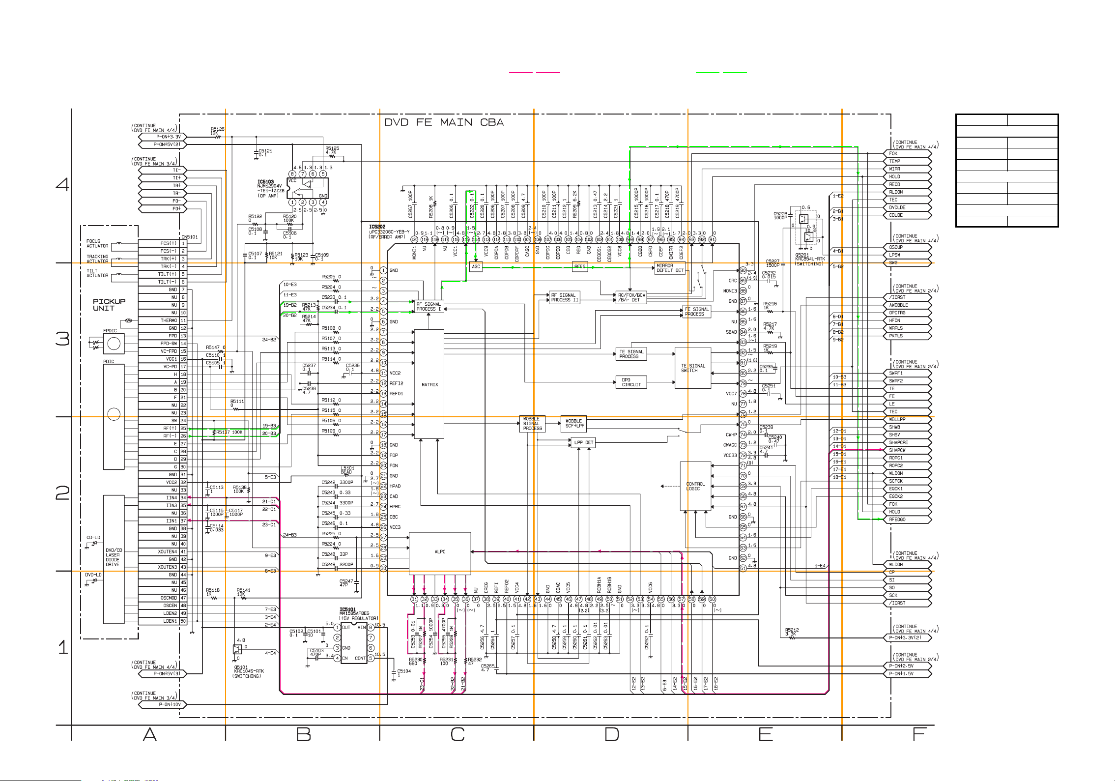
DVD FE Main 1/4 Schematic Diagram
DVD FE MAIN 1/4
Ref No. Position
IC5101 B-1
IC5103 B-4
IC5202 C-4
Q5101 B-1
Q5201 E-4
CN5101
A-4
CONNECTOR
ICS
TRANSISTORS
PB Video+Audio Signal (Digital)REC Video+Audio Signal (Digital)
A4
A3
B4
B3
C4
C3
D4
D3
E4
E3
F4
F3
A2
A1
B2
B1
1-8-3 1-8-4
C2
C1
D2
D1
E2
E1
F2
F1
E6502SCFM1
Page 27

DVD FE Main 2/4 Schematic Diagram
DVD FE MAIN 2/4
Ref No. Position
IC5301 H-4
IC5804 G-4
Q5301 K-1
Q5302 I-4
Q5802 G-4
CN5301
G-3
CONNECTOR
ICS
TRANSISTORS
PB Video+Audio Signal (Digital)REC Video+Audio Signal (Digital)
G4
G3
H4
H3
I4
I3
J4
J3
K4
K3
L4
L3
G2
G1
H2
H1
1-8-5 1-8-6
I2
I1
J2
J1
K2
K1
L2
L1
E6502SCFM2
Page 28

DVD FE Main 3/4 Schematic Diagram
DVD FE MAIN 3/4
Ref No. Position
IC5401 P-4
IC5501 P-3
IC5503 N-3
IC5601 N-3
IC5805 N-4
IC5806 N-3
CN5501 M-2
CN5502B R-1
CN5603 M-4
CN5603B R-1
CN5801
R-2
CONNECTORS
ICS
M4
M3
N4
N3
O4
O3
P4 Q4 R4
P3
Q3
R3
M2
M1
N2
N1
1-8-7 1-8-8
O2
O1
P2
P1
Q2
Q1
R2
R1
E6502SCFM3
Page 29

DVD FE Main 4/4 Schematic Diagram
DVD FE MAIN 4/4
Ref No. Position
IC5701 V-2
IC5703 U-2
IC5704 V-2
IC5705 V-4
IC5706 V-3
IC5707 W-2
CN5701 S-4
CN5602B
S-2
CONNECTORS
ICS
S4
S3
T4
T3
U4
U3
V4
V3
W4
W3
X4
X3
S2
S1
1-8-9
T2
T1
U2
U1
V2
V1
W2
W1
1-8-10
X2
X1
E6502SCFM4
Page 30

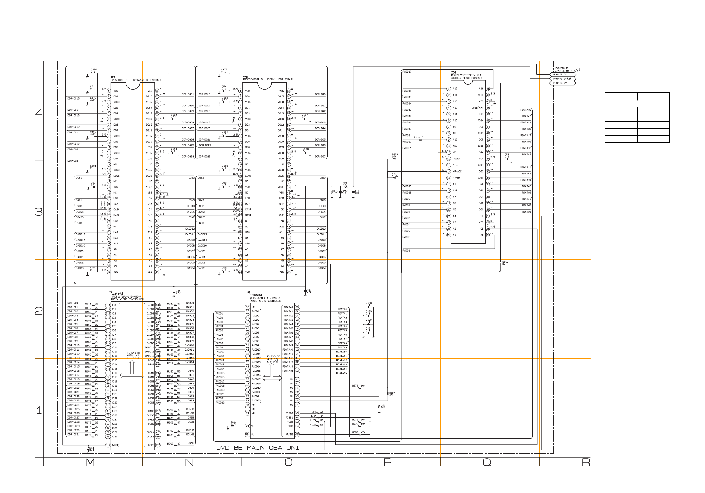
DVD BE Main 1/4 Schematic Diagram
DVD BE MAIN 1/4
Ref No. Position
IC3(1/6) D-3
IC9 B-4
IC12 B-2
IC13 D-1
IC17 C-4
Q16 D-4
Q17 D-4
Q18 E-4
Q19 B-4
Q20 A-4
Q21 E-2
CN7
F-4
ICS
CONNECTOR
TRANSISTORS
*1 Note:
1. The order of pins shown are different from that of IC3 itself.
2. IC3 is shown as IC3(1/6) through IC3(6/6) in DVD BE Main Schematic Diagram section.
REC Video+Audio Signal (Digital)
REC Video Signal (Digital)
REC Video Signal (Analog)
REC Audio Signal (Analog)
REC Audio Signal (Digital)
PB Video+Audio Signal (Digital)
PB Video Signal (Digital)
PB Video Signal
PB Audio Signal
PB Audio Signal (Digital)
A4
A3
B4
B3
C4
C3
D4
D3
E4
E3
F4
F3
A2
A1
B2
B1
1-8-11 1-8-12
C2
C1
D2
D1
E2
E1
F2
F1
E6502SCBM1
Page 31

DVD BE Main 2/4 Schematic Diagram
DVD BE MAIN 2/4
Ref No. Position
IC3(2/6) G-3
IC3(3/6) J-3
IC7 I-2
CN3
L-4
ICS
CONNECTOR
*1 Note:
1. The order of pins shown are different from that of IC3 itself.
2. IC3 is shown as IC3(1/6) through IC3(6/6) in DVD BE Main Schematic Diagram section.
G4
G3
H4
H3
I4
I3
J4
J3
K4
K3
L4
L3
G2
G1
1-8-13
H2
H1
I2
I1
J2
J1
K2
K1
1-8-14
L2
L1
E6502SCBM2
Page 32
DVD BE Main 3/4 Schematic Diagram
DVD BE MAIN 3/4
Ref No. Position
IC1 M-4
IC2 O-4
IC3(4/6) M-2
IC3(5/6) O-2
IC6
Q-4
ICS
*1 Note:
1. The order of pins shown are different from that of IC3 itself.
2. IC3 is shown as IC3(1/6) through IC3(6/6) in DVD BE Main Schematic Diagram section.
M4
M3
N4
N3
O4
O3
P4 Q4 R4
P3
Q3
R3
M2
M1
N2
N1
1-8-15 1-8-16
O2
O1
P2
P1
Q2
Q1
R2
R1
E6502SCBM3
Page 33

DVD BE Main 4/4 Schematic Diagram
DVD BE MAIN 4/4
Ref No. Position
IC3(6/6) V-4
IC19 S-2
CN1 X-4
CN6
S-2
ICS
CONNECTOR
*1 Note:
1. The order of pins shown are different from that of IC3 itself.
2. IC3 is shown as IC3(1/6) through IC3(6/6) in DVD BE Main Schematic Diagram section.
S4
S3
T4
T3
U4
U3
V4
V3
PB Video+Audio Signal (Digital)REC Video+Audio Signal (Digital)
W4
W3
X4
X3
S2
S1
1-8-17
T2
T1
U2
U1
V2
V1
W2
W1
1-8-18
X2
X1
E6502SCBM4
Page 34

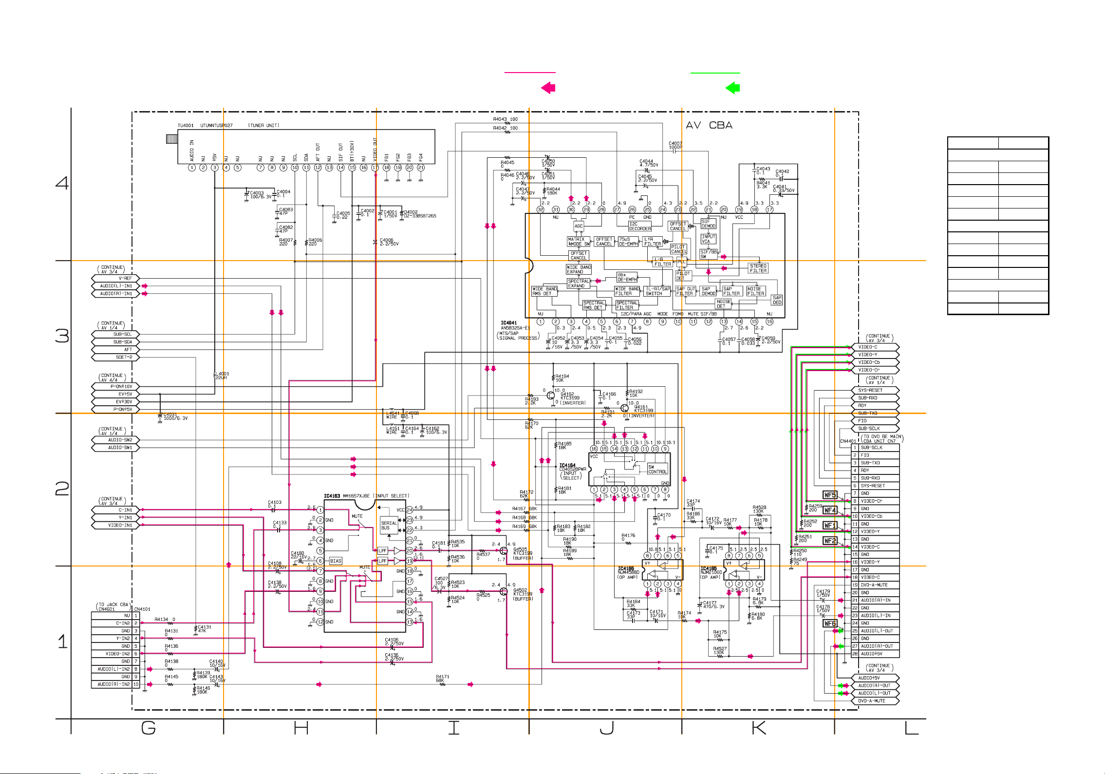
AV 1/4 Schematic Diagram
AV 1/4
Ref No. Position
IC4201
C-2
IC4202
E-2
Q4261
D-2
Q4262
E-1
CN2204 F-1
CN4202
F-2
CN4203 A-1
ICS
TRANSISTORS
CONNECTORS
A4
A3
B4
B3
C4
C3
D4
D3
E4
E3
F4
F3
A2
A1
B2
B1
1-8-19 1-8-20
C2
C1
D2
D1
E2
E1
F2
F1
E6502SCAV1
Page 35
AV 2/4 Schematic Diagram
AV 2/4
Ref No. Position
IC4041
J-3
IC4163
H-2
IC4164
J-2
IC4165
K-1
IC4166
J-1
Q4161
J-3
Q4162
J-3
Q4502
I-1
Q4505
I-2
CN4101 G-1
CN4401 L-2
ICS
TRANSISTORS
CONNECTOR
G4
G3
H4
H3
I4
I3
REC Video Signal (Analog)
REC Audio Signal (Analog)
J4
J3
PB Video Signal
PB Audio Signal
K4
K3
L4
L3
G2
G1
1-8-21
H2
H1
I2
I1
J2
J1
K2
K1
1-8-22
L2
L1
E6502SCAV2
Page 36

AV 3/4 Schematic Diagram
AV 3/4
Ref No. Position
IC4401
O-4
IC4421
N-2
Q4301
P-1
Q4424
P-2
Q4425
O-2
Q4426
P-2
Q4451 M-3
ICS
TRANSISTORS
REC Video Signal (Analog)
REC Audio Signal (Analog)
PB Video Signal
PB Audio Signal
M4
M3
N4 O4
N3
O3
REC Audio Signal (Digital)
P4 Q4 R4
P3
PB Audio Signal (Digital)
Q3
R3
M2
M1
N2
N1
1-8-23 1-8-24
O2
O1
P2
P1
Q2
Q1
R2
R1
E6502SCAV3
Page 37

AV 4/4 Schematic Diagram
AV 4/4
Ref No. Position
IC2101
T-1
IC4502
V-4
IC4503
V-3
Q2101
T-2
Q2102
T-3
Q2103
S-1
Q2203
V-3
Q2204
V-2
Q2205
V-2
Q2207
U-2
Q4501
W-2
CN2202
X-1
CN2203
X-1
CN4502 X-4
ICS
TRANSISTORS
CONNECTORS
F
A V
S4
S3
CAUTION
FOR CONTINUED PROTECTION AGAINST FIRE HAZARD,
REPLACE ONLY WITH THE SAME TYPE FUSE.
ATTENTION : POUR UNE PROTECTION CONTINUE LES RISQES
D'INCELE N'UTILISER QUE DES FUSIBLE DE MÊME TYPE.
RISK OF FIRE-REPLACE FUSE AS MARKED.
"This symbol means fast operating fuse."
"Ce symbole reprèsente un fusible à fusion rapide."
T4
T3
U4
U3
CAUTION !
Fixed voltage ( or Auto voltage selectable ) power supply circuit is used in this unit.
If Main Fuse (F2101) is blown, check to see that all components in the power supply
circuit are not defective before you connect the AC plug to the AC power supply.
Otherwise it may cause some components in the power supply circuit to fail.
NOTE :
The voltage for parts in hot circuit is measured using
hot GND as a common terminal.
V4
V3
REC Audio Signal (Digital)
W4
W3
PB Audio Signal (Digital)
X4
X3
S2
S1
1-8-25
T2
T1
U2
U1
V2
V1
W2
W1
1-8-26
X2
X1
E6502SCAV4
Page 38

FL Schematic Diagram
A3
B3
7G
REC
PM
REPEAT
FL2301 MATRIX CHART
7G 6G 5G 4G 3G 2G 1G
a
b
c
d
e
REC
f
PM
g
hh
6G
5G 4G 3G 2G 1G
VCD VCR
CD
T C
h
g
h
C3
DVD
c
a
d
g
b
SLP
ef
R
W
XP SP
LP EP
SEP
P.SCAN
D3
i
REPEAT
a
b
c
d
e
f
gg
CD
a
b
c
d
e
f
g
T
a
b
c
d
e
f
g
VCD VCR DVD
a
b
c
d
e
f
g
a
b
c
d
e
f
g
P.SCAN
C
XP
SP
LP
EP
SLP
SEP
W
R
A2
B2
C2
D2
FL
Ref No. Position
IC
IC2301
CONNECTOR
CN2301 A-1
C-2
A1
B1
1-8-27 1-8-28
C1
D1
E6502SCFL
Page 39
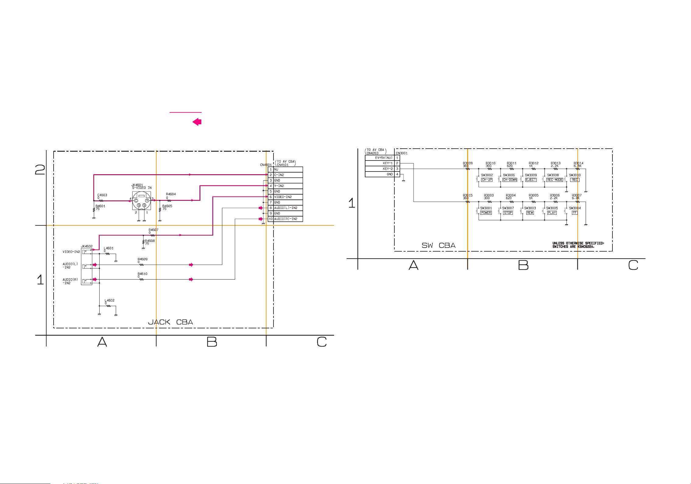
Jack Schematic Diagram
SW Schematic Diagram
REC Video Signal (Analog)
REC Audio Signal (Analog)
A2
A1
B2
B1
C2
C1
A1
B1 C1
E6502SCSW
1-8-29
E6502SCJK
1-8-30
Page 40

AV CBA Top View
CAUTION !
Fixed voltage ( or Auto voltage selectable ) power supply circuit is used in this unit.
If Main Fuse (F2101) is blown, check to see that all components in the power supply
circuit are not defective before you connect the AC plug to the AC power supply.
Otherwise it may cause some components in the power supply circuit to fail.
CAUTION
F
A V
FOR CONTINUED PROTECTION AGAINST FIRE HAZARD,
REPLACE ONLY WITH THE SAME TYPE FUSE.
ATTENTION : POUR UNE PROTECTION CONTINUE LES RISQES
D'INCELE N'UTILISER QUE DES FUSIBLE DE MÊME TYPE.
RISK OF FIRE-REPLACE FUSE AS MARKED.
"This symbol means fast operating fuse."
"Ce symbole reprèsente un fusible à fusion rapide."
NOTE :
The voltage for parts in hot circuit is measured
using hot GND as a common terminal.
1-8-31
1-8-32
BE6500F01023A
Page 41

AV CBA Bottom View
AV CBA
Ref No. Position
IC2101
B-2
IC4041
E-2
IC4163
E-2
IC4164
D-2
IC4165
D-2
IC4166
D-2
IC4201
E-3
IC4202
E-4
IC4401
E-2
IC4421
C-2
IC4502
D-3
IC4503
E-3
Q2101
A-2
Q2102
A-2
Q2103
A-2
Q2203
B-2
Q2204
B-2
Q2205
C-2
Q2207
B-1
Q4161
C-3
Q4162
C-3
Q4261
E-3
Q4262
E-3
Q4301
C-1
Q4424
D-1
Q4425
D-1
Q4426
C-1
Q4451
C-2
Q4501
C-2
Q4502
C-1
Q4505
E-1
CN2204
A-3
CN2202
B-3
CN2203
C-1
CN4101
E-4
CN4202
E-4
CN4203
F-3
CN4401
E-2
CN4502
D-3
ICS
TRANSISTORS
CONNECTORS
WF3
C4411
Plus lead
WF5
PIN 8 OF
CN4401
WF7
PIN 18 OF
CN4502
WF4
PIN 10 OF
CN4401
WF1
PIN 12 OF
CN4401
CAUTION !
Fixed voltage ( or Auto voltage selectable ) power supply circuit is used in this unit.
If Main Fuse (F2101) is blown, check to see that all components in the power supply
circuit are not defective before you connect the AC plug to the AC power supply.
Otherwise it may cause some components in the power supply circuit to fail.
CAUTION
F
A V
WF2
PIN 14 OF
CN4401
FOR CONTINUED PROTECTION AGAINST FIRE HAZARD,
REPLACE ONLY WITH THE SAME TYPE FUSE.
ATTENTION : POUR UNE PROTECTION CONTINUE LES RISQES
D'INCELE N'UTILISER QUE DES FUSIBLE DE MÊME TYPE.
RISK OF FIRE-REPLACE FUSE AS MARKED.
"This symbol means fast operating fuse."
"Ce symbole reprèsente un fusible à fusion rapide."
WF6
PIN 25 OF
CN4401
NOTE :
The voltage for parts in hot circuit is measured
using hot GND as a common terminal.
1-8-33
1-8-34
BE6500F01023A
Page 42

FL CBA Top View
Jack CBA Top View
FL CBA Bottom View
1-8-35
BE6500F01023D
Jack CBA Bottom View
BE6500F01023B
1-8-36
Page 43

SW CBA Top View
SW CBA Bottom View
1-8-37 1-8-38
BE6500F01023C
Page 44

WF1
Pin 12 of CN4401
WAVEFORMS
WF5
Pin 8 of CN4401
VIDEO-Y 0.2V 20µsec
WF2
Pin 14 of CN4401
VIDEO-C 0.2V 20
WF3
C4411 PLUS LEAD
VIDEO-Cr
WF6
Pin 25 of CN4401
µ
sec
A-OUT(L)
WF7
Pin 18 of CN4502
0.2V 20µsec
1V 0.1µsec
VIDEO-CVBS 0.5V 20
WF4
Pin 10 of CN4401
VIDEO-Cb
0.2V 20µsec
µ
µ
sec
SPDIF 1V 0.1
sec
NOTE:
Input: COLOR BAR SIGNAL
(WITH 1KHz AUDIO SIGNAL)
1-9-1
R1NWF
Page 45

WIRING DIAGRAM
FAN
AC CORD
REAR
CN2301
W11
EV+5V 11-FL 22F1 33F2 44FL-SDA 55FL-SCL 6
CN2204
DIGITAL
AUDIO OUT
AUDIO-R
OUT2
AUDIO-L
OUT2
AUDIO-R
OUT1
AUDIO-L
OUT1
AUDIO-R
IN
AUDIO-L
IN
VIDEO-Cr
OUT
VIDEO-Cb
OUT
VIDEO-Y
OUT
VIDEO
OUT
VIDEO
IN
S-VIDEO
OUT
S-VIDEO
IN
2GND
1FAN+10.5V
8BUP+5V
7GND
6RW-RESET
5RW-VPP
4RW-SDA
3RW-SCLK
2RW-BUSY
(NO CONNECTION)
1RW-OEX
FL CBA
(BE6500F01023D)
FL-STB 77REMOTE 88GND 9
6
AV CBA
(BE6500F01023A)
CN2203
CN4202
FRONT
9
CN4203
CN4401
CN4502
W10
2727
2525
W8
W7
AUDIO-L
IN2
AUDIO-R
S-VIDEO
IN
CN4601
NU 11C-IN2 22GND 33Y-IN2 44GND 55VIDEO-IN2 66GND 77AUDIO(L)-IN2 88GND 99AUDIO(R)-IN2 10
CN4101 W12
GND 44
KEY-2 33
KEY-1 22
EV+5V(NU) 11
CN3001
AUDIO+5V 2828
AUDIO(R)-OUT
GND 2626
AUDIO(L)-OUT
GND 2424
AUDIO(L)-IN 2323
GND 2222
AUDIO(R)-IN 2121
GND 2020
DVD-A-MUTE 1919
VIDEO-C 1818
GND 1717
VIDEO-Y 1616
GND 1515
VIDEO-C 1414
CN7
GND 1313
VIDEO-Y 1212
GND 1111
VIDEO-Cb 1010
GND 99
VIDEO-Cr 88
GND 77
SYS-RESET 66
SUB-RXD 55
RDY 44
SUB-TXD 33
FID 22
SUB-SCLK 11
IN2
(BE6500F01023B)
JACK CBA
CN2202
SW CBA
(BE6500F01023C)
CN3
DVD BE MAIN CBA UNIT
SPDIF 1818
GND 1717
GND 1616
P-ON+5V 1515
GND 1414
GND 1313
P-ON+3.3V 1212
P-ON+3.3V 1111
P-ON+3.3V 1010
GND 99
CN6
P-ON+2.5V 88
P-ON+2.5V 77
P-ON+2.5V 66
GND 55
VI+2.5V 44
VI+2.5V 33
VI+2.5V 22
VI+2.5V 11
VIDEO
IN2
(NO CONNECTION)
10
4 P-ON+5V
3 GND
2 GND
1 P-ON+10V
SYS-RESET
9
JTCK
8
GND
7
JTDO
6
P-ON+3.3V
5
JTMS
4
JTRST
3
(NO CONNECTION)
JTDI
2
TMODE0
1
2525
2222
CN1
10SCISEL1
9SCISEL0
8P-ON+3.3V(2)
7GND
6JL-CLK
5/RST-S
4SCK1
3TXD
2RXD
1P-ON+5V(4)
4P-ON+5V
3GND
2GND
1P-ON+10V
GND 4040
DASP(NU) 3939
CS1B 3838
CS0B 3737
DA2 3 636
DA0 3 535
PDIAG(NU) 3434
DA1 3 333
NU 3232
INTRQ 3131
GND 3030
DMACKB 2929
GND 2828
ORDY 2727
GND 2626
IORB
GND 2424
DIORB 2323
GND
DMARQB 2121
NU 2020
GND 1919
CN5301
DD15 1818
DD0 1717
DD14 1616
DD1 1515
DD13 1414
DD2 1313
DD12 1212
DD3 1111
DD11 1010
DD4 99
DD10 88
DD5 77
DD9 66
DD6 55
DD8 44
DD7 33
GND 22
RESETB 11
CN5701
CN5801
CN5101
DVD FE MAIN CBA UNIT
CN5501
LDEN1
LDEN2
OSCEN
OSCMOD
NU
NU
GND
XOUTEN3
GND
XOUTEN4
NU
NU
GND
IIN1
NU
IIN3
IIN4
NU
VCC2
GND
G
D
C
E
RF(-)
RF(+)
SW
NU
NU
F
B
A
H
VC-PD
VCC1
VC-FPD
FPD-SW
FPD
GND
THERMO
GND
TRK(-)
TRK(+)
FCS(+)
CN5602B
CN5603
CN5603B
CN5502B
VHHWHW+
HVHV+
HUHU+
VCC
U
V
W
9NU
8NU
7
6 TILT(-)
5 TILT(+)
4
3
2 FCS(-)
1
9
8
7
6
5
4
3
2
1
50
49
48
47
46
45
44
43
42
41
40
39
38
37
36
35
34
33
32
31
30
29
28
27
26
25
24
23
22
21
20
19
18
17
16
15
14
13
12
11
10 NU
T-SCN3 33
T-SCN2 22
GND 11
M
M
11
10
CD-LDDVD-LD
DVD/CD LASER DIODE DRIVE
PICKUP UNIT
PDIC
FPDIC
ACTUATOR
TILT
ACTUATOR
TRACKING
ACTUATOR
FOCUS
TRAY IN
LOADER
TRAY OUT
SLED
SENSOR
FFC6001
ENCODER
SLED
MOTOR
LOADING
MOTOR
M
SPINDLE
MOTOR
CBA
CBA
DVD MECHA
DVD MECHA & FE ASSEMBLY
1-10-1
E6502WI
Page 46

FIRMWARE RENEWAL MODE
1. Turn the power on and remove the disc on the tray.
2. To put the DVD recorder into version up mode,
press [CM SKIP], [6], [5], and [4] buttons on the
remote control unit in the order. The tray will open
automatically.
Fig. a appears on the screen and Fig. b appears on
the VFD.
Firm Update Mode
Please insert a Disc.
Fig. a Version Up Mode Screen
Fig. b VFD in Version Up Mode
ver. R1F0467S1E
3. Load the disc for version up.
Fig. c appears on the screen. The file on the top is
highlighted as the default.
When there is only one file to exist, Step 4 will start
automatically.
Firm Update Mode
UPDATE DISC
JPN
TEST
RIF0025S1E
RIF0035S1E
RIF0056S1E
RIF0078S1E
ver. R1F0467S1E
4. Select the firmware version using arrow buttons,
then press [ENTER].
Fig. d appears on the screen and Fig.E appears on
the VFD. The DVD recorder starts updating.
Firm Update Mode
R1F0525S1E
File Loading...
*1
Fig. d Programming Mode Screen
Fig. e VFD in Programming Mode (Example)
ver. R1F0467S1E
The appearance shown in *1 of Fig. d is described
as follows.
AppearanceNo. State
1
File Loading... Sending files into the memory.
Firmware
2
Updating...
Firm Update
Failure
Writing new version data.
Failed in updating.
5. After updating is finished, the tray opens automatically.
Fig. f appears on the screen and Fig. g appears on
the VFD.
Firm Update Mode
R1F0525S1E
ver. R1F0467S1E
Fig. c Update Disc Screen
B/E Firmware
Update End
Fig. f Completed Program Mode Screen
Fig. g VFD in Completed Program Mode
At this time, no buttons are available.
6. Press [POWER] button to turn the power off. Then
press it again.
1-11-1 E6500TEST
Page 47
Tray in
Tray in
Tray out
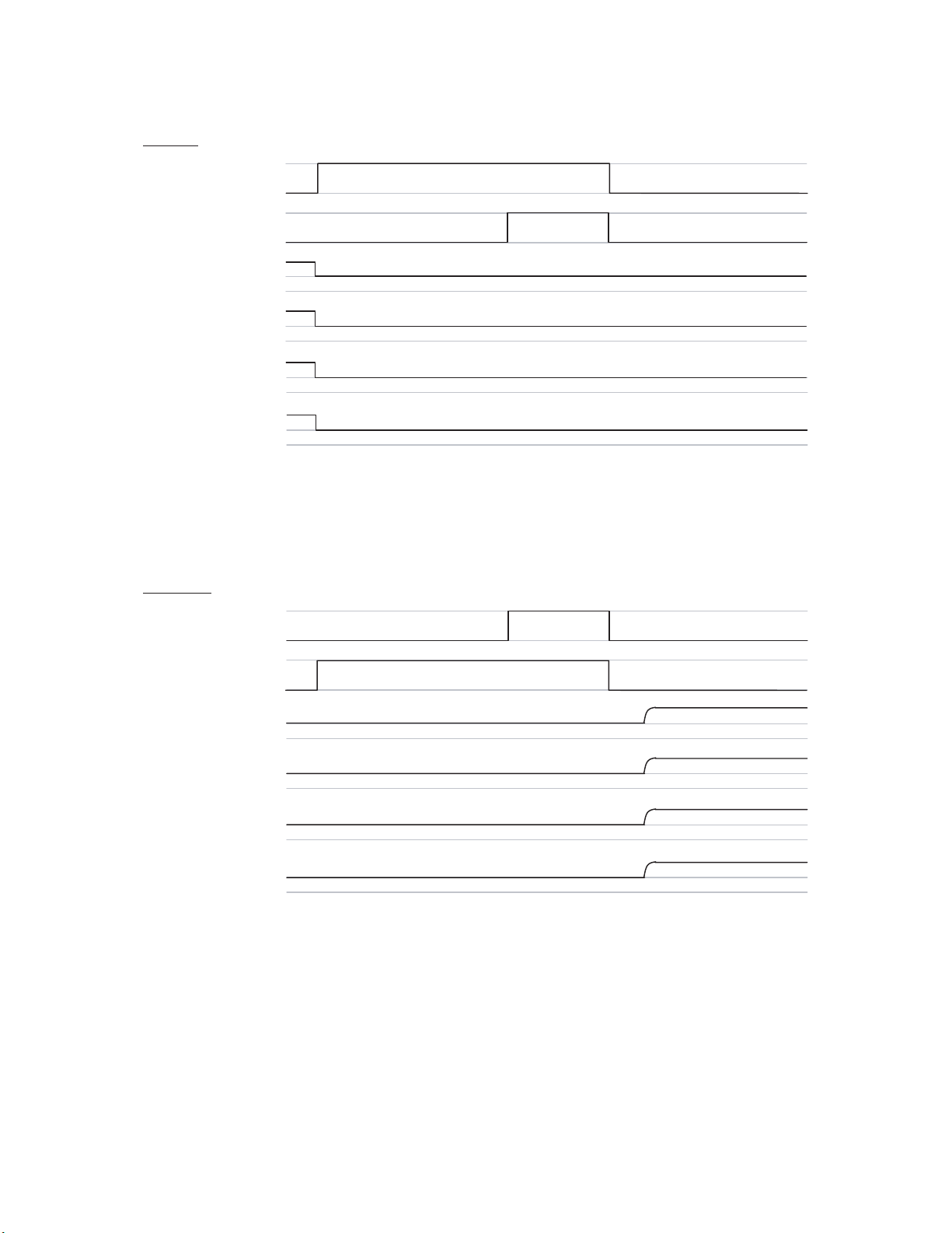
SYSTEM CONTROL TIMING CHARTS
5.0V
0V
5.0V
0V
Sled Drive
Disc Drive
Focus Drive
Tracking Drive
Tray out
Tray in
Tray out
Sled Drive
1.35V
0V
1.35V
0V
1.35V
0V
1.35V
0V
5.0V
0V
5.0V
0V
1.35V
0V
Disc Drive
Focus Drive
Tracking Drive
1.35V
0V
1.35V
0V
1.35V
0V
1-12-1 E6TI
Page 48

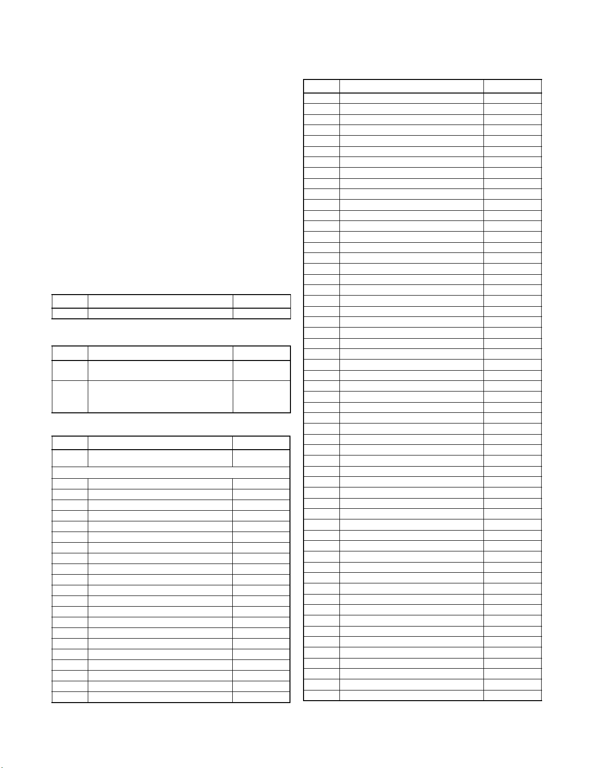
Spin up
Tray in
Tray out
5.0V
0V
5.0V
0V
Sled Drive
Disc Drive
Focus Drive
Tracking Drive
Playing
Tray in
Tray out
Sled Drive
1.35V
0V
1.35V
0V
1.35V
0V
1.35V
0V
5.0V
0V
5.0V
0V
1.35V
0V
Disc Drive
Focus Drive
Tracking Drive
1.35V
0V
1.35V
0V
1.35V
0V
1-12-2 E6TI
Page 49

IC PIN FUNCTION DESCRIPTIONS
IC4201 [ SUB MICRO CONTROLLER ]
Pin
No.
IN/
OUT
1
IN
2
IN
3-
4INREMOTE
5-
6-
7-
8 OUT FL-STB
9OUTFL-CLK
10 OUT FL-SDA
11 -
12 OUT RW-BUSY
13 IN RW-SCLK
Signal
Name
KEY-1 Key Data Input 1
KEY-2 Key Data Input 2
N.U. Not Used
N.U. Not Used
N.U. Not Used
N.U. Not Used
N.U. Not Used
Name Function
Remote Signal Input
Serial Interface Strobe
Serial Clock
Serial Data
For Flash Memory Writing
For Flash Memory Writing
Pin
No.
IN/
OUT
31 -
32 -
33 -
34 -
35 -
36 -
37 -
38 -
39 OUT V-MUTE
40 OUT
41 IN RDY
42 IN FID
Signal
Name
N.U. Not Used
N.U. Not Used
N.U. Not Used
N.U. Not Used
N.U. Not Used
N.U. Not Used
N.U. Not Used
N.U. Not Used
SYS-
RESET
Name Function
Video Mute Control Signal
System Reset Signal
Ready/Busy
communication Control
with Main Micro Controller
Video Presence Detector
Signal
14 -
IN/
15
OUT
16 IN P-DOWN
17 -
18 IN RW-VPP
19 IN RESET
20 IN XCIN
21 OUT XCOUT
22 IN XIN
23 OUT XOUT
24 - GND
25 OUT PWSW
26 -
27 -
28 -
29 -
30 -
N.U. Not Used
RW-SDA
N.U. Not Used
N.U. Not Used
N.U. Not Used
N.U. Not Used
N.U. Not Used
N.U. Not Used
For Flash Memory Writing
Power Voltage Down
Detector Signal
For Flash Memory Writing
Micro Controller Reset
Signal
Sub Clock Input
Sub Clock Output
Main Clock Input
Main Clock Output
Ground
Main Power Control Signal
43 -
44 -
45 OUT
46 OUT
47 OUT A-MUTE
48 -
49 IN RW-OEX
50 OUT SUB-SCLK
51 OUT SUB-TXD
52 IN SUB-RXD
53 OUT SUB-SCL
IN/
54
OUT
55 -
56 -
57 IN VCC
58 IN V-REF
N.U. Not Used
N.U. Not Used
AUDIO-
SW1
AUDIO-
SW2
N.U. Not Used
SUB-SDA
N.U. Not Used
N.U. Not Used
Audio Input Select Signal
Audio Input Select Signal
Audio Mute Control Signal
For Flash Memory Writing
Communication Clock with
Main Micro Controller
Transmission Data to Main
Micro Controller
Reception Data from Main
Micro Controller
Serial Clock
Serial Data
+5V Power Supply
Reference Voltage
1-13-1 E6502PIN
Page 50

Pin
No.
IN/
OUT
59 - AVSS
Signal
Name
Name Function
Ground
IC2301 [ PT6313-S-TP ]
Pin
No.
IN/
OUT
Signal
Name
Name Function
60 -
61 OUT
62 IN AFT
63 IN
64 IN POW-SW
N.U. Not Used
REG-
CONT
SDET-1
Power Regurator Control
Signal
Tuner Voltage Input Signal
Aspect Ratio Detector
Signal
Abnormal Voltage
Detection
1 IN CLK
2 IN STB
3 -
4 -
5 - VSS
6 - VDD
7 OUT a
8 OUT b
9 OUT c
10 OUT d
11 OUT e
12 IN f
13 IN g
14 OUT h
15 - VEE
16 OUT i
N.U. Not Used
N.U. Not Used
Serial Clock
Serial Interface Strobe
GND
Power Supply
Segment Output
Pull Down Level
Segment Output
17
18 6G
19 5G
OUT
20 4G
21 3G
22 2G
23 1G
24 - VDD
25 - VSS
26 IN OSC
27 -
28 IN DIN
7G
N.U. Not Used
Grid Output
Power Supply
GND
Oscillator Input
Serial Data Input
1-13-2 E6502PIN
Page 51

LEAD IDENTIFICATIONS
2SC2120-Y(TPE2)
KTC3203(Y)
E C B E C B
MM1657XJBE
24
1
13
12
NJM4558D
NJM2100D
8
1
5
4
2SC2785(H)
KTA1267(Y)
KTC3199(GR,BL)
PT6313-S-TP
SC16313
28
1
15
14
PQ070XF01SZ
1234
2SK3757(Q)
GDS
M38039MC-177HP
48
49
64
1
PST597INR
54
123
33
16
32
17
AN5832SA-E1
32
1
CD4052BPWR
MM1637XVBE
16
1
17
16
S2Y52
9
8
E C B
Note:
C
E
A: Anode
K: Cathode
E: Emitter
C: Collector
B: Base
R: Reference
G: Gate
D: Drain
S: Source
PS2561A-1(W)
PS2561A-1(Q)
A
K
1-14-1 E6502LE
Page 52

Cabinet
EXPLODED VIEWS
See Electrical Parts List
for parts with this mark.
Some Ref. Numbers are
not in sequence.
W10
2B9
DVD BE Main
CBA Unit
2L071
2B6
A1X
2L021
W8
2L081
W7
2L011
SW CBA
2L081
2L063
2L021
A2
2L021
2B7
AC2101
2L081
2L071
2L042
2B1
Jack CBA
2L082
2B4
2B4
2L042
A14
W12
2L031
A13
2B8
2L031
A5
W11
1B1
2B10
2L031
2L083
FL CBA
A4
F2101
AV CBA
2L022
2L012
A12
2L051
2L023
2L051
A3
FM1001
2B5
A5
1-15-1 E6502EX
Page 53

Packing
Some Ref. Numbers
are not in sequence.
X3
X10
S2
X1
X4
X2
X6
X5
S2
S3
2B12
Unit
A13
S1
1-15-2 E6502EX
Page 54

MECHANICAL PARTS LIST
PRODUCT SAFETY NOTE: Products marked with a #
have special characteristics important to safety. Before
replacing any of these components, read carefully the
product safety notice in this service manual. Don't
degrade the safety of the product through improper servicing.
NOTE:
Parts that are not assigned part numbers (---------) are
not available.
Ref. No. Description Part No.
A1X FRONT ASSEMBLY E6502CD 1VM220137
A2 TOP COVER 0VM101334
A3 REAR PANEL E6502CD 1VM220136
A4 CHASSIS 0VM101335
A5 FOOT 0VM416122
A12 MANUFACTURE LABEL ---------A13 LABEL, BAR CODE HB400UD ---------A14 LABEL (B) ---------1B1 DVD MECHA & FE ASSEMBLY N7810FUQ
2B1 HOLDER D 0VM306680
2B4 BE EARTH SPRING 0VM416236
2B5 FAN HOLDER E6500UD 0VM306843
2B7 FAN SHEET 0VM306869
2B8# CAUTION LABEL ---------2B9 CLOTH BE 0VM416495
2B10 WASHER 1VM420041
2B12 ANTITHEFT LABEL HA861CD ---------2L011 SCREW, B-TIGHT M3X8 BIND HEAD + GBKB3080
2L012 SCREW, B-TIGHT M3X8 BIND HEAD + GBKB3080
2L021 SCREW, S-TIGHT M3X8 BIND CROM GBCS3060
2L022 SCREW, S-TIGHT M3X8 BIND CROM GBCS3060
2L023 SCREW, S-TIGHT M3X8 BIND CROM GBCS3060
2L031 SCREW, S-TIGHT M3X10 BIND HEAD+ GBMS3100
2L042 SCREW, S-TIGHT M3X5 BIND HEAD+ GBMS3050
2L051 SCREW, P-TIGHT 3X10 BIND HEAD+ GBCP3100
2L063 SCREW, P-TIGHT M2.6X8 BIND HEAD+ GBMP9080
2L071 SCREW M3X6 BIND + –¡¦Š‹ SBM33060
2L081 SCREW, S-TIGHT M3X6 CUP HEAD+ GCMS3060
2L082 SCREW, S-TIGHT M3X6 CUP HEAD+ GCMS3060
2L083 SCREW, S-TIGHT M3X6 CUP HEAD+ GCMS3060
FM1001 DC FAN MOTOR D05U-12TS1 03(UX) MMEZR12NH001
PACKING
S1 SHIPPING CARTON E6502CD 1VM320292
S2 STYROFOAM E6500UD 0VM101341
S3 UNIT, BAG E5500UD 0VM411683
ACCESSORIES
X1 REMOTE CONTROL UNIT DVD 0842 VCZF01RR NB001UD
X2 DRY BATTERY R6P/2S or XB0M451T0001
DRY BATTERY ES-GR6M-C XB0M571GLP01
X3 AV CORD TSCKA-Y/RW100 or WPZ0102TM015
AV CORD RCA(M*2)TO RCA(M*2) WPZ0102LTE01
Ref. No. Description Part No.
X4 RF CABLE 2.5C-2V or WPZ0901TM002
RF CABLE DC95M95M001 WPZ0901CAB01
X5 ACCESSORY BAG E56A0UD 0VM413280
X6 QUICK GUIDE CANADA 1VMN20176
X10# OWNERS MANUAL E6502CD 1VMN20174
20040617 1-16-1 E6502CA
Page 55
ELECTRICAL PARTS LIST
PRODUCT SAFETY NOTE: Products marked with a #
have special characteristics important to safety. Before
replacing any of these components, read carefully the
product safety notice in this service manual. Don't
degrade the safety of the product through improper servicing.
NOTES:
1. Parts that are not assigned part numbers (---------)
are not available.
2. Tolerance of Capacitors and Resistors are noted
with the following symbols.
C.....±0.25% D.....±0.5% F.....±1%
G.....±2% J......±5% K.....±10%
M.....±20% N.....±30% Z.....+80/-20%
DVD BE MAIN CBA UNIT
Ref. No. Description Part No.
DVD BE MAIN CBA UNIT N78F0AUP
AV CBA ASSEMBLY
Ref. No. Description Part No.
AV CBA ASSEMBLY
Consists of the following:
AV CBA (SUB-A)
JACK CBA (SUB-B)
SW CBA (SUB-C)
FL CBA (SUB-D)
AV CBA
Ref. No. Description Part No.
AV CBA (SUB-A)
Consists of the followings
CAPACITORS
C2101# METALLIZED FILM CAP. 0.068µF/250V K or CT2E683DC011
# METALLIZED FILM CAP. 0.068µF/275V K CT2E683HJE06
C2102# SAFETY CAP. 2200pF/250V or CCG2EMA0F222
# SAFETY CAP. 2200pF/250V CCD2EMA0E222
C2103 ELECTROLYTIC CAPACIT0R 150µF/200V or CA2D151S6012
ALMINIUM ELECTROLYTIC CAP150µF/200V CA2D151NC088
C2104 CERAMIC CAP. B K 0.01µF/500V CCD2JKP0B103
C2105 CERAMIC CAP. B K 120pF/500V CCD2JKP0B121
C2107 CERAMIC CAP.(AX) B K 3300pF/50V CA1J332TU011
C2108 CERAMIC CAP.(AX) X K 5600pF/16V CCA1CKT0X562
C2110 ELECTROLYTIC CAP. 10µF/16V M or CE1CMASDL100
ELECTROLYTIC CAP. 10µF/16V M CE1CMASTL100
C2111 FILM CAP.(P) 0.022µF/50V J or CMA1JJS00223
FILM CAP.(P) 0.022µF/50V J CA1J223MS029
C2201 ELECTROLYTIC CAP. 10µF/50V M or CE1JMASDL100
ELECTROLYTIC CAP. 10µF/50V M CE1JMASTL100
C2202 CHIP CERAMIC CAP.(1608) F Z 0.1µF/50V or CHD1JZ30F104
CHIP CERAMIC CAP.(1608) F Z 0.1µF/25V CHD1EZ30F104
C2203 ELECTROLYTIC CAP. 3300µF/6.3V SL or CE0KMZADL332
ELECTROLYTIC CAP. 3300µF/6.3V M CE0KMZPTL332
C2204 ELECTROLYTIC CAP. 1000µF/6.3V M or CE0KMASDL102
0VSA14794
----------
----------
----------
----------
------------
Ref. No. Description Part No.
ELECTROLYTIC CAP. 1000µF/6.3V M CE0KMASTL102
C2205 CERAMIC CAP. B K 220pF/500V CCD2JKP0B221
C2206 ELECTROLYTIC CAP. 4700µF/6.3V SL or CE0KMZADL472
ELECTROLYTIC CAP. 4700µF/6.3V M CE0KMZPTL472
C2207 ELECTROLYTIC CAP. 1000µF/6.3V M or CE0KMASDL102
ELECTROLYTIC CAP. 1000µF/6.3V M CE0KMASTL102
C2208 ELECTROLYTIC CAP. 1000µF/16V M or CE1CMASDL102
ELECTROLYTIC CAP. 1000µF/16V M CE1CMASTL102
C2209 ELECTROLYTIC CAP. 470µF/16V M or CE1CMASDL471
ELECTROLYTIC CAP. 470µF/16V M CE1CMASTL471
C2210 ELECTROLYTIC CAP. 100µF/16V M or CE1CMASDL101
ELECTROLYTIC CAP. 100µF/16V M CE1CMASTL101
C2211 CHIP CERAMIC CAP.(1608) B K 0.01µF/50V CHD1JK30B103
C2212 CHIP CERAMIC CAP.(1608) B K 0.033µF/50V CHD1JK30B333
C2213 CERAMIC CAP. B K 470pF/500V CCD2JKP0B471
C2216 CHIP CERAMIC CAP.(1608) B K 0.01µF/50V CHD1JK30B103
C2217 CHIP CERAMIC CAP.(1608) B K 3300pF/50V CHD1JK30B332
C2219 ELECTROLYTIC CAP. 22µF/50V M or CE1JMASDL220
ELECTROLYTIC CAP. 22µF/50V M CE1JMASTL220
C2220 CERAMIC CAP. CH J 47pF/50V CCD1JJSCH470
C4001 ELECTROLYTIC CAP. 1µF/50V M or CE1JMASDL1R0
ELECTROLYTIC CAP. 1µF/50V M CE1JMASTL1R0
C4002 CHIP CERAMIC CAP.(1608) F Z 0.1µF/50V or CHD1JZ30F104
CHIP CERAMIC CAP.(1608) F Z 0.1µF/25V CHD1EZ30F104
C4003 ELECTROLYTIC CAP. 100µF/6.3V M or CE0KMASDL101
ELECTROLYTIC CAP. 100µF/6.3V M CE0KMASTL101
C4004 CHIP CERAMIC CAP.(1608) F Z 0.1µF/50V or CHD1JZ30F104
CHIP CERAMIC CAP.(1608) F Z 0.1µF/25V CHD1EZ30F104
C4005 CHIP CERAMIC CAP.(1608) B K 0.22µF/16V CHD1CK30B224
C4006 ELECTROLYTIC CAP. 2.2µF/50V M NP CP1JMASNC2R2
C4007 CHIP CERAMIC CAP.(1608) CH J 1000pF/50V CHD1JJ3CH102
C4041 ELECTROLYTIC CAP. 0.33µF/50V M or CE1JMASDLR33
ELECTROLYTIC CAP. 0.33µF/50V M CE1JMASTLR33
C4042 CHIP CERAMIC CAP.(1608) B K 0.1µF/25V CHD1EK30B104
C4043 CHIP CERAMIC CAP.(1608) B K 0.1µF/25V CHD1EK30B104
C4044 ELECTROLYTIC CAP. 4.7µF/50V M or CE1JMASDL4R7
ELECTROLYTIC CAP. 4.7µF/50V M CE1JMASTL4R7
C4045 ELECTROLYTIC CAP. 2.2µF/50V M or CE1JMASDL2R2
ELECTROLYTIC CAP. 2.2µF/50V M CE1JMASTL2R2
C4046 ELECTROLYTIC CAP. 2.2µF/50V M or CE1JMASDL2R2
ELECTROLYTIC CAP. 2.2µF/50V M CE1JMASTL2R2
C4047 ELECTROLYTIC CAP. 2.2µF/50V M or CE1JMASDL2R2
ELECTROLYTIC CAP. 2.2µF/50V M CE1JMASTL2R2
C4050 ELECTROLYTIC CAP. 1µF/50V M or CE1JMASDL1R0
ELECTROLYTIC CAP. 1µF/50V M CE1JMASTL1R0
C4051 ELECTROLYTIC CAP. 1µF/50V M or CE1JMASDL1R0
ELECTROLYTIC CAP. 1µF/50V M CE1JMASTL1R0
C4052 ELECTROLYTIC CAP. 10µF/16V M or CE1CMASDL100
ELECTROLYTIC CAP. 10µF/16V M CE1CMASTL100
C4053 ELECTROLYTIC CAP. 3.3µF/50V M or CE1JMASDL3R3
ELECTROLYTIC CAP. 3.3µF/50V M CE1JMASTL3R3
C4054 ELECTROLYTIC CAP. 3.3µF/50V M or CE1JMASDL3R3
ELECTROLYTIC CAP. 3.3µF/50V M CE1JMASTL3R3
C4055 CHIP CERAMIC CAP.(1608) F Z 0.1µF/50V or CHD1JZ30F104
CHIP CERAMIC CAP.(1608) F Z 0.1µF/25V CHD1EZ30F104
C4056 CHIP CERAMIC CAP.(1608) B K 0.022µF/50V CHD1JK30B223
C4057 CHIP CERAMIC CAP.(1608) B K 0.1µF/25V CHD1EK30B104
20040617 1-17-1 E6502EL
Page 56

Ref. No. Description Part No.
C4058 CHIP CERAMIC CAP.(1608) B K 0.033µF/50V CHD1JK30B333
C4059 ELECTROLYTIC CAP. 2.2µF/50V M or CE1JMASDL2R2
ELECTROLYTIC CAP. 2.2µF/50V M CE1JMASTL2R2
C4068 CHIP CERAMIC CAP.(1608) F Z 0.1µF/50V or CHD1JZ30F104
CHIP CERAMIC CAP.(1608) F Z 0.1µF/25V CHD1EZ30F104
C4082 CHIP CERAMIC CAP.(1608) CH J 47pF/50V CHD1JJ3CH470
C4083 CHIP CERAMIC CAP.(1608) CH J 47pF/50V CHD1JJ3CH470
C4101 CHIP RES.(1608) 1/10W 0 Ω RRXAZR5Z0000
C4102 CHIP RES.(1608) 1/10W J 47k Ω RRXAJR5Z0473
C4103 CHIP CERAMIC CAP.(1608) F Z 0.1µF/50V or CHD1JZ30F104
CHIP CERAMIC CAP.(1608) F Z 0.1µF/25V CHD1EZ30F104
C4106 ELECTROLYTIC CAP. 2.2µF/50V M or CE1JMASDL2R2
ELECTROLYTIC CAP. 2.2µF/50V M CE1JMASTL2R2
C4108 ELECTROLYTIC CAP. 2.2µF/50V M or CE1JMASDL2R2
ELECTROLYTIC CAP. 2.2µF/50V M CE1JMASTL2R2
C4111 ELECTROLYTIC CAP. 10µF/16V M or CE1CMASDL100
ELECTROLYTIC CAP. 10µF/16V M CE1CMASTL100
C4113 ELECTROLYTIC CAP. 10µF/16V M or CE1CMASDL100
ELECTROLYTIC CAP. 10µF/16V M CE1CMASTL100
C4131 CHIP RES.(1608) 1/10W J 47k Ω RRXAJR5Z0473
C4133 CHIP CERAMIC CAP.(1608) F Z 0.1µF/50V or CHD1JZ30F104
CHIP CERAMIC CAP.(1608) F Z 0.1µF/25V CHD1EZ30F104
C4136 ELECTROLYTIC CAP. 2.2µF/50V M or CE1JMASDL2R2
ELECTROLYTIC CAP. 2.2µF/50V M CE1JMASTL2R2
C4138 ELECTROLYTIC CAP. 2.2µF/50V M or CE1JMASDL2R2
ELECTROLYTIC CAP. 2.2µF/50V M CE1JMASTL2R2
C4140 ELECTROLYTIC CAP. 10µF/16V M or CE1CMASDL100
ELECTROLYTIC CAP. 10µF/16V M CE1CMASTL100
C4143 ELECTROLYTIC CAP. 10µF/16V M or CE1CMASDL100
ELECTROLYTIC CAP. 10µF/16V M CE1CMASTL100
C4162 ELECTROLYTIC CAP. 100µF/6.3V M or CE0KMASDL101
ELECTROLYTIC CAP. 100µF/6.3V M CE0KMASTL101
C4164 CHIP CERAMIC CAP.(1608) F Z 0.1µF/50V or CHD1JZ30F104
CHIP CERAMIC CAP.(1608) F Z 0.1µF/25V CHD1EZ30F104
C4166 CHIP CERAMIC CAP.(1608) F Z 0.1µF/50V or CHD1JZ30F104
CHIP CERAMIC CAP.(1608) F Z 0.1µF/25V CHD1EZ30F104
C4170 CHIP CERAMIC CAP.(1608) F Z 0.1µF/50V or CHD1JZ30F104
CHIP CERAMIC CAP.(1608) F Z 0.1µF/25V CHD1EZ30F104
C4171 ELECTROLYTIC CAP. 10µF/16V M or CE1CMASDL100
ELECTROLYTIC CAP. 10µF/16V M CE1CMASTL100
C4172 ELECTROLYTIC CAP. 10µF/16V M or CE1CMASDL100
ELECTROLYTIC CAP. 10µF/16V M CE1CMASTL100
C4173 CHIP CERAMIC CAP.(1608) CH J 33pF/50V CHD1JJ3CH330
C4174 CHIP CERAMIC CAP.(1608) CH J 33pF/50V CHD1JJ3CH330
C4175 CHIP CERAMIC CAP.(1608) F Z 0.1µF/50V or CHD1JZ30F104
CHIP CERAMIC CAP.(1608) F Z 0.1µF/25V CHD1EZ30F104
C4177 ELECTROLYTIC CAP. 470µF/6.3V M or CE0KMASDL471
ELECTROLYTIC CAP. 470µF/6.3V M CE0KMASTL471
C4178 ELECTROLYTIC CAP. 1µF/50V M or CE1JMASDL1R0
ELECTROLYTIC CAP. 1µF/50V M CE1JMASTL1R0
C4179 ELECTROLYTIC CAP. 1µF/50V M or CE1JMASDL1R0
ELECTROLYTIC CAP. 1µF/50V M CE1JMASTL1R0
C4180 ELECTROLYTIC CAP. 22µF/16V M or CE1CMASDL220
ELECTROLYTIC CAP. 22µF/16V M CE1CMASTL220
C4181 CHIP CERAMIC CAP.(1608) F Z 0.1µF/50V or CHD1JZ30F104
CHIP CERAMIC CAP.(1608) F Z 0.1µF/25V CHD1EZ30F104
C4203 CHIP CERAMIC CAP.(1608) F Z 0.1µF/50V or CHD1JZ30F104
CHIP CERAMIC CAP.(1608) F Z 0.1µF/25V CHD1EZ30F104
C4204 ELECTROLYTIC CAP. 22µF/16V M or CE1CMASDL220
ELECTROLYTIC CAP. 22µF/16V M CE1CMASTL220
C4206 CHIP CERAMIC CAP.(1608) B K 0.01µF/50V CHD1JK30B103
Ref. No. Description Part No.
C4207 CHIP CERAMIC CAP.(1608) CH J 22pF/50V CHD1JJ3CH220
C4208 CHIP CERAMIC CAP.(1608) CH J 22pF/50V CHD1JJ3CH220
C4210 CHIP CERAMIC CAP.(1608) F Z 0.1µF/50V or CHD1JZ30F104
CHIP CERAMIC CAP.(1608) F Z 0.1µF/25V CHD1EZ30F104
C4261 ELECTROLYTIC CAP. 1000µF/6.3V M or CE0KMASDL102
ELECTROLYTIC CAP. 1000µF/6.3V M CE0KMASTL102
C4280 CHIP CERAMIC CAP.(1608) CH J 270pF/50V CHD1JJ3CH271
C4281 CHIP CERAMIC CAP.(1608) CH J 270pF/50V CHD1JJ3CH271
C4282 CHIP CERAMIC CAP.(1608) CH J 270pF/50V CHD1JJ3CH271
C4301 CHIP CERAMIC CAP.(1608) F Z 0.1µF/50V or CHD1JZ30F104
CHIP CERAMIC CAP.(1608) F Z 0.1µF/25V CHD1EZ30F104
C4302 ELECTROLYTIC CAP. 47µF/6.3V M H7 or CE0KMASSL470
ELECTROLYTIC CAP. 47µF/6.3V M CE0KMASTL470
C4401 CHIP CERAMIC CAP.(1608) B K 0.01µF/50V CHD1JK30B103
C4402 CHIP CERAMIC CAP.(1608) F Z 0.1µF/50V or CHD1JZ30F104
CHIP CERAMIC CAP.(1608) F Z 0.1µF/25V CHD1EZ30F104
C4403 CHIP CERAMIC CAP.(1608) F Z 0.1µF/50V or CHD1JZ30F104
CHIP CERAMIC CAP.(1608) F Z 0.1µF/25V CHD1EZ30F104
C4404 CHIP CERAMIC CAP.(1608) F Z 0.1µF/50V or CHD1JZ30F104
CHIP CERAMIC CAP.(1608) F Z 0.1µF/25V CHD1EZ30F104
C4405 CHIP CERAMIC CAP.(1608) F Z 0.1µF/50V or CHD1JZ30F104
CHIP CERAMIC CAP.(1608) F Z 0.1µF/25V CHD1EZ30F104
C4406 ELECTROLYTIC CAP. 470µF/6.3V M or CE0KMASDL471
ELECTROLYTIC CAP. 470µF/6.3V M CE0KMASTL471
C4407 CHIP CERAMIC CAP.(1608) B K 0.01µF/50V CHD1JK30B103
C4408 ELECTROLYTIC CAP. 22µF/16V M or CE1CMASDL220
ELECTROLYTIC CAP. 22µF/16V M CE1CMASTL220
C4410 CHIP CERAMIC CAP.(1608) F Z 0.1µF/50V or CHD1JZ30F104
CHIP CERAMIC CAP.(1608) F Z 0.1µF/25V CHD1EZ30F104
C4411 ELECTROLYTIC CAP. 470µF/6.3V M or CE0KMASDL471
ELECTROLYTIC CAP. 470µF/6.3V M CE0KMASTL471
C4413 ELECTROLYTIC CAP. 1000µF/6.3V M or CE0KMASDL102
ELECTROLYTIC CAP. 1000µF/6.3V M CE0KMASTL102
C4415 ELECTROLYTIC CAP. 470µF/6.3V M or CE0KMASDL471
ELECTROLYTIC CAP. 470µF/6.3V M CE0KMASTL471
C4416 ELECTROLYTIC CAP. 470µF/6.3V M or CE0KMASDL471
ELECTROLYTIC CAP. 470µF/6.3V M CE0KMASTL471
C4421 ELECTROLYTIC CAP. 470µF/6.3V M or CE0KMASDL471
ELECTROLYTIC CAP. 470µF/6.3V M CE0KMASTL471
C4422 ELECTROLYTIC CAP. 10µF/16V M or CE1CMASDL100
ELECTROLYTIC CAP. 10µF/16V M CE1CMASTL100
C4424 CHIP CERAMIC CAP.(1608) CH J 270pF/50V CHD1JJ3CH271
C4425 CHIP CERAMIC CAP.(1608) CH J 47pF/50V CHD1JJ3CH470
C4426 ELECTROLYTIC CAP. 10µF/16V M or CE1CMASDL100
ELECTROLYTIC CAP. 10µF/16V M CE1CMASTL100
C4429 ELECTROLYTIC CAP. 10µF/16V M or CE1CMASDL100
ELECTROLYTIC CAP. 10µF/16V M CE1CMASTL100
C4431 CHIP CERAMIC CAP.(1608) CH J 270pF/50V CHD1JJ3CH271
C4432 CHIP CERAMIC CAP.(1608) CH J 47pF/50V CHD1JJ3CH470
C4433 ELECTROLYTIC CAP. 10µF/16V M or CE1CMASDL100
ELECTROLYTIC CAP. 10µF/16V M CE1CMASTL100
C4434 CHIP CERAMIC CAP.(1608) F Z 0.1µF/50V or CHD1JZ30F104
CHIP CERAMIC CAP.(1608) F Z 0.1µF/25V CHD1EZ30F104
C4451 ELECTROLYTIC CAP. 47µF/16V M or CE1CMASDL470
ELECTROLYTIC CAP. 47µF/16V M CE1CMASTL470
C4452 ELECTROLYTIC CAP. 1000µF/6.3V M or CE0KMASDL102
ELECTROLYTIC CAP. 1000µF/6.3V M CE0KMASTL102
C4502 ELECTROLYTIC CAP. 47µF/16V M or CE1CMASDL470
ELECTROLYTIC CAP. 47µF/16V M CE1CMASTL470
C4503 ELECTROLYTIC CAP. 100µF/6.3V M or CE0KMASDL101
ELECTROLYTIC CAP. 100µF/6.3V M CE0KMASTL101
20040617 1-17-2 E6502EL
Page 57

Ref. No. Description Part No.
C4505 ELECTROLYTIC CAP. 100µF/6.3V M or CE0KMASDL101
ELECTROLYTIC CAP. 100µF/6.3V M CE0KMASTL101
C4506 CHIP CERAMIC CAP.(1608) F Z 0.1µF/50V or CHD1JZ30F104
CHIP CERAMIC CAP.(1608) F Z 0.1µF/25V CHD1EZ30F104
C4509 ELECTROLYTIC CAP. 100µF/16V M or CE1CMASDL101
ELECTROLYTIC CAP. 100µF/16V M CE1CMASTL101
C4517 ELECTROLYTIC CAP. 100µF/6.3V M or CE0KMASDL101
ELECTROLYTIC CAP. 100µF/6.3V M CE0KMASTL101
C4518 ELECTROLYTIC CAP. 100µF/6.3V M or CE0KMASDL101
ELECTROLYTIC CAP. 100µF/6.3V M CE0KMASTL101
C4525 CHIP CERAMIC CAP.(1608) F Z 0.1µF/50V or CHD1JZ30F104
CHIP CERAMIC CAP.(1608) F Z 0.1µF/25V CHD1EZ30F104
C4526 CHIP CERAMIC CAP.(1608) F Z 0.1µF/50V or CHD1JZ30F104
CHIP CERAMIC CAP.(1608) F Z 0.1µF/25V CHD1EZ30F104
C4527 ELECTROLYTIC CAP. 100µF/6.3V M NP CP0KMASNC101
C4531 ELECTROLYTIC CAP. 1000µF/6.3V M or CE0KMASDL102
ELECTROLYTIC CAP. 1000µF/6.3V M CE0KMASTL102
C4534 CHIP CERAMIC CAP.(1608) CH J 270pF/50V CHD1JJ3CH271
C4536 CHIP CERAMIC CAP.(1608) F Z 0.1µF/50V or CHD1JZ30F104
CHIP CERAMIC CAP.(1608) F Z 0.1µF/25V CHD1EZ30F104
C4537 CHIP CERAMIC CAP.(1608) F Z 0.1µF/50V or CHD1JZ30F104
CHIP CERAMIC CAP.(1608) F Z 0.1µF/25V CHD1EZ30F104
C4538 CHIP CERAMIC CAP.(1608) F Z 0.1µF/50V or CHD1JZ30F104
CHIP CERAMIC CAP.(1608) F Z 0.1µF/25V CHD1EZ30F104
CONNECTORS
CN2202 CONNECTOR BASE 4P B4B-XH-2 J3XHC04JG014
CN2203 PH CONNECTOR, TOP 2P B2B-PH-K-S J3PHC02JG001
CN4203 FMN CONNECTOR, TOP 4P 04FMN-BTRK JCFNG04JG002
CN4401 FMN CONNECTOR, TOP 28P 28FMN-BTRK JCFNG28JG002
CN4502 FFC/FPC CONNECTOR, 18P 00 6232 018 006
800 or
FFC CONNECTOR IMSA-9615S-18A-PP-A JC96J18ER007
JC62G18TM010
DIODES
D2101 DIODE 1N5397-B NDLZ001N5397
D2102 DIODE 1N5397-B NDLZ001N5397
D2103 DIODE 1N5397-B NDLZ001N5397
D2104 DIODE 1N5397-B NDLZ001N5397
D2105 SWITCHING DIODE 1SS133(T-77) or QDTZ001SS133
SWITCHING DIODE 1N4148M NDTZ01N4148M
D2106 RECTIFIER DIODE BA157 NDQZ000BA157
D2107 SWITCHING DIODE 1SS133(T-77) or QDTZ001SS133
SWITCHING DIODE 1N4148M NDTZ01N4148M
D2108 SWITCHING DIODE 1SS133(T-77) or QDTZ001SS133
SWITCHING DIODE 1N4148M NDTZ01N4148M
D2109 SWITCHING DIODE 1SS133(T-77) or QDTZ001SS133
SWITCHING DIODE 1N4148M NDTZ01N4148M
D2110 SWITCHING DIODE 1SS133(T-77) or QDTZ001SS133
SWITCHING DIODE 1N4148M NDTZ01N4148M
D2111 PCB JUMPER D0.6-P5.0 JW5.0T
D2201 RECTIFIER DIODE BA157 NDQZ000BA157
D2203 RECTIFIER DIODE BA157 NDQZ000BA157
D2204 SCHOTTKY BARRIER DIODE SB340 NDQZ000SB340
D2206 SCHOTTKY BARRIER DIODE SB140 NDQZ000SB140
D2207 SCHOTTKY BARRIER DIODE SB340 NDQZ000SB340
D2209 SCHOTTKY BARRIER DIODE SB340 NDQZ000SB340
D2212 SCHOTTKY BARRIER DIODE SB3B0 NDQZ000SB3B0
D2213 ZENER DIODE DZ-15BSAT265 or NDTA00DZ15BS
ZENER DIODE MTZJT-7715A QDTA00MTZJ15
D2214 RECTIFIER DIODE BA157 NDQZ000BA157
D2215 ZENER DIODE DZ-18BSAT265 or NDTA00DZ18BS
ZENER DIODE MTZJT-7718A QDTA00MTZJ18
Ref. No. Description Part No.
D2217 SWITCHING DIODE 1SS133(T-77) or QDTZ001SS133
SWITCHING DIODE 1N4148M NDTZ01N4148M
D2218 ZENER DIODE DZ-6.8BSBT265 or NDTB0DZ6R8BS
ZENER DIODE MTZJT-776.8B QDTB0MTZJ6R8
D2220 SWITCHING DIODE 1SS133(T-77) or QDTZ001SS133
SWITCHING DIODE 1N4148M NDTZ01N4148M
D2221 SWITCHING DIODE 1SS133(T-77) or QDTZ001SS133
SWITCHING DIODE 1N4148M NDTZ01N4148M
D2222 DIODE 1N5397-B NDLZ001N5397
D2223 PCB JUMPER D0.6-P5.0 JW5.0T
D2224 DIODE 1N5397-B NDLZ001N5397
D4002 ZENER DIODE DZ-33BSBT265 or NDTB00DZ33BS
ZENER DIODE MTZJT-7733B QDTB00MTZJ33
D4261 ZENER DIODE Z02W3.0V-X-RTK ND1XZ02W3R0V
D4452 ZENER DIODE DZ-5.6BSCT265 or NDTC0DZ5R6BS
ZENER DIODE MTZJT-775.6C QDTC0MTZJ5R6
D4501 ZENER DIODE DZ-11BSBT265 or NDTB00DZ11BS
ZENER DIODE MTZJT-7711B QDTB00MTZJ11
D4502 SWITCHING DIODE 1SS133(T-77) or QDTZ001SS133
SWITCHING DIODE 1N4148M NDTZ01N4148M
D4503 SWITCHING DIODE 1SS133(T-77) or QDTZ001SS133
SWITCHING DIODE 1N4148M NDTZ01N4148M
ICS
IC2101# PHOTOCOUPLER PS2561A-1(W) or QPEWPS2561A1
# PHOTOCOUPLER PS2561A-1(Q) QPEQPS2561A1
IC4041 IC:MTS DECORDER AN5832SA-E1 QSZBA0TMS003
IC4163 IC(VIDEO SW) MM1657XJBE QSZBA0TMM100
IC4164 IC(ANALOG SW) CD4052BPWR NSZBA0TTY142
IC4165 IC(OP AMP) NJM2100D QSZBA0SJR069
IC4166 IC:OP AMP NJM4558D QSZBA0SJR006
IC4201 IC(CPU) M38039MC-177HP QSZAA0RHT037
IC4202 IC(RESET) PST597INR QSZBA0TMM105
IC4401 DRIVER FOR DVD MM1637XVBE QSZBA0TMM102
IC4421 IC:OP AMP NJM4558D QSZBA0SJR006
IC4502 VOLTAGE REGULATOR PQ070XF01SZ QSZBA0SSH026
IC4503 VOLTAGE REGULATOR PQ070XF01SZ QSZBA0SSH026
COILS
L2101# LINE FILTER 27MH TLF14CB2730R4 or LLBG00ZTU034
# LINE FILTER 26MH ELF15N004A or LLBG00ZMS042
# LINE FILTER 27MH CSA-LF199A LLBG00ZSA008
L2105 BEAD CORE B16 RH 4X3X2 or XL03003XM001
BEAD CORE HF70BB4.1X3X2 XL03003TE001
L2106 BEAD CORE B16 RH 3.5X10X1.3 or XL03010XM001
BEAD CORE HF70BB3.5X10X1.3 XL03010TE001
L2202 INDUCTOR(15UH) CWKB-150K or LLC150KKV005
CHOKE COIL(15UH) LHL10NB150K LLARKGQTU150
L2203 INDUCTOR(18UH) CWKB-180K or LLC180KKV005
CHOKE COIL(18UH) LHL10NB180K LLARKGQTU180
L2206 CHIP RES.(2125) 1/8W 0 Ω RRX8ZR6Z0000
L4001 CHOKE COIL 22µH-K LLBD00PKV006
L4041 PCB JUMPER D0.6-P5.0 JW5.0T
L4161 PCB JUMPER D0.6-P5.0 JW5.0T
L4301 INDUCTOR(0.47µH K) LAP02TAR47K LLAXKATTUR47
L4305 CHIP RES.(1608) 1/10W 0 Ω RRXAZR5Z0000
L4306 CHIP RES.(1608) 1/10W 0 Ω RRXAZR5Z0000
L4310 CHIP RES.(1608) 1/10W 0 Ω RRXAZR5Z0000
L4314 CHIP RES.(1608) 1/10W 0 Ω RRXAZR5Z0000
L4315 CHIP RES.(1608) 1/10W 0 Ω RRXAZR5Z0000
L4316 CHIP RES.(1608) 1/10W 0 Ω RRXAZR5Z0000
L4401 PCB JUMPER D0.6-P5.0 JW5.0T
20040617 1-17-3 E6502EL
Page 58

Ref. No. Description Part No.
L4501 CHOKE COIL 22µH-K LLBD00PKV006
L4502 CHOKE COIL 22µH-K LLBD00PKV006
TRANSISTORS
Q2101 TRANSISTOR KTC3199(GR) or NQS10KTC3199
TRANSISTOR KTC3199(BL) or NQS50KTC3199
TRANSISTOR 2SC2785(H) QQSH02SC2785
Q2102# FET 2SK3757(Q) QFWZ02SK3757
Q2103 TRANSISTOR KTC3199(GR) or NQS10KTC3199
TRANSISTOR KTC3199(BL) or NQS50KTC3199
TRANSISTOR 2SC2785(H) QQSH02SC2785
Q2203 TRANSISTOR S2Y52(FUNAI) QQWZ000S2Y52
Q2204 TRANSISTOR S2Y52(FUNAI) QQWZ000S2Y52
Q2205 TRANSISTOR 2SC2120-Y(TPE2) or QQSY02SC2120
TRANSISTOR KTC3203(Y) or NQSY0KTC3203
TRANSISTOR 2SC2120-O-TPE2 or QQS002SC2120
TRANSISTOR KTC3203(0) NQS00KTC3203
Q2207 TRANSISTOR KTA1267(Y) NQSY0KTA1267
Q4161 TRANSISTOR KTC3199(GR) or NQS10KTC3199
TRANSISTOR KTC3199(BL) or NQS50KTC3199
TRANSISTOR 2SC2785(H) QQSH02SC2785
Q4162 TRANSISTOR KTC3199(GR) or NQS10KTC3199
TRANSISTOR KTC3199(BL) or NQS50KTC3199
TRANSISTOR 2SC2785(H) QQSH02SC2785
Q4261 TRANSISTOR KTA1267(Y) NQSY0KTA1267
Q4262 TRANSISTOR KTC3199(GR) or NQS10KTC3199
TRANSISTOR KTC3199(BL) or NQS50KTC3199
TRANSISTOR 2SC2785(H) QQSH02SC2785
Q4301 TRANSISTOR KTC3199(GR) or NQS10KTC3199
TRANSISTOR KTC3199(BL) or NQS50KTC3199
TRANSISTOR 2SC2785(H) QQSH02SC2785
Q4424 TRANSISTOR KTC3199(GR) or NQS10KTC3199
TRANSISTOR KTC3199(BL) or NQS50KTC3199
TRANSISTOR 2SC2785(H) QQSH02SC2785
Q4425 TRANSISTOR KTA1267(Y) NQSY0KTA1267
Q4426 TRANSISTOR KTC3199(GR) or NQS10KTC3199
TRANSISTOR KTC3199(BL) or NQS50KTC3199
TRANSISTOR 2SC2785(H) QQSH02SC2785
Q4451 TRANSISTOR KTC3199(GR) or NQS10KTC3199
TRANSISTOR KTC3199(BL) or NQS50KTC3199
TRANSISTOR 2SC2785(H) QQSH02SC2785
Q4501 TRANSISTOR KTC3199(GR) or NQS10KTC3199
TRANSISTOR KTC3199(BL) or NQS50KTC3199
TRANSISTOR 2SC2785(H) QQSH02SC2785
Q4502 TRANSISTOR KTC3199(GR) or NQS10KTC3199
TRANSISTOR KTC3199(BL) or NQS50KTC3199
TRANSISTOR 2SC2785(H) QQSH02SC2785
Q4505 TRANSISTOR KTC3199(GR) or NQS10KTC3199
TRANSISTOR KTC3199(BL) or NQS50KTC3199
TRANSISTOR 2SC2785(H) QQSH02SC2785
RESISTORS
R2101# CARBON RES. 1/2W J 3.3M Ω RCX2335DP001
R2101 GLASS GLAZE RES. 1/2W J 3.3M Ω RXX2JZLZ0335
R2102 CARBON RES. 1/4W J 2.7M Ω RCX4JATZ0275
R2103 CARBON RES. 1/4W J 2.7M Ω RCX4JATZ0275
R2104 CARBON RES. 1/4W J 820 Ω RCX4JATZ0821
R2105 METAL OXIDE FILM RES. 2W J 1.5 Ω or RN021R5ZU001
METAL OXIDE FILM RES. 2W J 1.5 Ω or RN021R5DP004
METAL OXIDE FILM RES. 2W J 1.5 Ω RN021R5KE010
R2106 METAL OXIDE FILM RES. 1W J 12k Ω or RN01123ZU001
METAL OXIDE FILM RES. 1W J 12k Ω or RN01123DP003
Ref. No. Description Part No.
METAL OXIDE FILM RES. 1W J 12k Ω RN01123KE010
R2107 CARBON RES. 1/4W J 470k Ω RCX4JATZ0474
R2108 CARBON RES. 1/4W J 15k Ω RCX4JATZ0153
R2109 METAL RESISTER. 2W J 0.56 Ω or RN02R56ZU001
METAL OXIDE FILM RES. 2W J 0.56 Ω or RN02R56DP004
METAL OXIDE FILM RES. 2W J 0.56 Ω RN02R56KE010
R2111 CARBON RES. 1/4W J 1k Ω RCX4JATZ0102
R2113 CARBON RES. 1/4W J 680k Ω RCX4JATZ0684
R2114 CARBON RES. 1/4W J 100k Ω RCX4JATZ0104
R2115 CARBON RES. 1/4W J 10k Ω RCX4JATZ0103
R2116 CARBON RES. 1/4W J 100k Ω RCX4JATZ0104
R2117 CARBON RES. 1/4W J 470k Ω RCX4JATZ0474
R2118 CARBON RES. 1/4W J 1k Ω RCX4JATZ0102
R2119 PCB JUMPER D0.6-P5.0 JW5.0T
R2201 CARBON RES. 1/4W J 1.5k Ω RCX4JATZ0152
R2202 CHIP RES.(1608) 1/10W J 390 Ω RRXAJR5Z0391
R2203 CHIP RES.(1608) 1/10W J 470 Ω RRXAJR5Z0471
R2204 PCB JUMPER D0.6-P5.0 JW5.0T
R2205 CARBON RES. 1/4W J 1.2k Ω RCX4JATZ0122
R2207 CHIP RES.(1608) 1/10W F 2.4k Ω or RRXAFR5H2401
CHIP RES.(1608) 1/10W F 2.4k Ω RRXAFR5J2401
R2208 CHIP RES.(1608) 1/10W J 1.8k Ω RRXAJR5Z0182
R2209 CHIP RES.(1608) 1/10W J 1.8k Ω RRXAJR5Z0182
R2210 CHIP RES.(1608) 1/10W J 4.7k Ω RRXAJR5Z0472
R2211 CHIP RES.(1608) 1/10W F 5.6k Ω or RRXAFR5H5601
CHIP RES.(1608) 1/10W F 5.6k Ω RRXAFR5J5601
R2212 CARBON RES. 1/4W J 7.5 Ω RCX4JATZ07R5
R2214 CHIP RES.(1608) 1/10W 0 Ω RRXAZR5Z0000
R2215 CHIP RES.(1608) 1/10W J 4.7k Ω RRXAJR5Z0472
R2216 CARBON RES. 1/4W J 180 Ω RCX4JATZ0181
R2217 CHIP RES.(1608) 1/10W J 4.7k Ω RRXAJR5Z0472
R2218 CARBON RES. 1/4W J 680 Ω RCX4JATZ0681
R2219 CHIP RES.(1608) 1/10W J 4.7k Ω RRXAJR5Z0472
R2220 CHIP RES.(1608) 1/10W 0 Ω RRXAZR5Z0000
R2228 PCB JUMPER D0.6-P15.0 JW15.0T
R2232 CARBON RES. 1/4W J 10k Ω RCX4JATZ0103
R2233 CARBON RES. 1/4W J 6.8k Ω RCX4JATZ0682
R2235 PCB JUMPER D0.6-P15.0 JW15.0T
R2236 PCB JUMPER D0.6-P15.0 JW15.0T
R2239 CARBON RES. 1/4W J 4.7k Ω RCX4JATZ0472
R2240 CARBON RES. 1/4W J 1.5k Ω RCX4JATZ0152
R2243 CHIP RES.(1608) 1/10W F 150 Ω or RRXAFR5H1500
CHIP RES.(1608) 1/10W F 150 Ω RRXAFR5J1500
R2244 CARBON RES. 1/4W J 27 Ω RCX4JATZ0270
R2245 CARBON RES. 1/4W J 180 Ω RCX4JATZ0181
R2246 CARBON RES. 1/4W J 680 Ω RCX4JATZ0681
R4006 CHIP RES.(1608) 1/10W J 220 Ω RRXAJR5Z0221
R4007 CHIP RES.(1608) 1/10W J 220 Ω RRXAJR5Z0221
R4041 CHIP RES.(1608) 1/10W J 3.3k Ω RRXAJR5Z0332
R4042 CHIP RES.(1608) 1/10W J 100 Ω RRXAJR5Z0101
R4043 CHIP RES.(1608) 1/10W J 100 Ω RRXAJR5Z0101
R4044 CHIP RES.(1608) 1/10W J 180k Ω RRXAJR5Z0184
R4045 CHIP RES.(1608) 1/10W 0 Ω RRXAZR5Z0000
R4046 CHIP RES.(1608) 1/10W 0 Ω RRXAZR5Z0000
R4102 CHIP RES.(1608) 1/10W J 75 Ω RRXAJR5Z0750
R4103 CHIP RES.(1608) 1/10W J 75 Ω RRXAJR5Z0750
R4107 CHIP RES.(1608) 1/10W J 75 Ω RRXAJR5Z0750
R4108 CHIP RES.(1608) 1/10W 0 Ω RRXAZR5Z0000
R4109 CHIP RES.(1608) 1/10W J 180k Ω RRXAJR5Z0184
R4114 CHIP RES.(1608) 1/10W 0 Ω RRXAZR5Z0000
R4115 CHIP RES.(1608) 1/10W J 180k Ω RRXAJR5Z0184
20040617 1-17-4 E6502EL
Page 59

Ref. No. Description Part No.
R4131 CHIP RES.(1608) 1/10W 0 Ω RRXAZR5Z0000
R4134 CHIP RES.(1608) 1/10W 0 Ω RRXAZR5Z0000
R4136 CHIP RES.(1608) 1/10W 0 Ω RRXAZR5Z0000
R4138 CHIP RES.(1608) 1/10W 0 Ω RRXAZR5Z0000
R4139 CHIP RES.(1608) 1/10W J 180k Ω RRXAJR5Z0184
R4145 CHIP RES.(1608) 1/10W 0 Ω RRXAZR5Z0000
R4146 CHIP RES.(1608) 1/10W J 180k Ω RRXAJR5Z0184
R4167 CHIP RES.(1608) 1/10W F 68k Ω or RRXAFR5H6802
CHIP RES.(1608) 1/10W F 68.0k Ω RRXAFR5J6802
R4168 CHIP RES.(1608) 1/10W F 68k Ω or RRXAFR5H6802
CHIP RES.(1608) 1/10W F 68.0k Ω RRXAFR5J6802
R4169 CHIP RES.(1608) 1/10W F 68k Ω or RRXAFR5H6802
CHIP RES.(1608) 1/10W F 68.0k Ω RRXAFR5J6802
R4170 CHIP RES.(1608) 1/10W F 62k Ω or RRXAFR5H6202
CHIP RES.(1608) 1/10W F 62k Ω RRXAFR5J6202
R4171 CHIP RES.(1608) 1/10W F 68k Ω or RRXAFR5H6802
CHIP RES.(1608) 1/10W F 68.0k Ω RRXAFR5J6802
R4172 CHIP RES.(1608) 1/10W F 62k Ω or RRXAFR5H6202
CHIP RES.(1608) 1/10W F 62k Ω RRXAFR5J6202
R4174 CHIP RES.(1608) 1/10W F 10k Ω or RRXAFR5H1002
CHIP RES.(1608) 1/10W F 10k Ω RRXAFR5J1002
R4175 CHIP RES.(1608) 1/10W F 10k Ω or RRXAFR5H1002
CHIP RES.(1608) 1/10W F 10k Ω RRXAFR5J1002
R4176 CHIP RES.(1608) 1/10W 0 Ω RRXAZR5Z0000
R4177 CHIP RES.(1608) 1/10W F 10k Ω or RRXAFR5H1002
CHIP RES.(1608) 1/10W F 10k Ω RRXAFR5J1002
R4178 CHIP RES.(1608) 1/10W F 10k Ω or RRXAFR5H1002
CHIP RES.(1608) 1/10W F 10k Ω RRXAFR5J1002
R4179 CHIP RES.(1608) 1/10W J 6.8k Ω RRXAJR5Z0682
R4180 CHIP RES.(1608) 1/10W J 6.8k Ω RRXAJR5Z0682
R4181 CHIP RES.(1608) 1/10W J 18k Ω RRXAJR5Z0183
R4182 CHIP RES.(1608) 1/10W J 18k Ω RRXAJR5Z0183
R4183 CHIP RES.(1608) 1/10W J 18k Ω RRXAJR5Z0183
R4184 CHIP RES.(1608) 1/10W F 33.0k Ω or RRXAFR5H3302
CHIP RES.(1608) 1/10W F 33.0k Ω RRXAFR5J3302
R4185 CHIP RES.(1608) 1/10W J 18k Ω RRXAJR5Z0183
R4186 CHIP RES.(1608) 1/10W F 33.0k Ω or RRXAFR5H3302
CHIP RES.(1608) 1/10W F 33.0k Ω RRXAFR5J3302
R4189 CHIP RES.(1608) 1/10W J 18k Ω RRXAJR5Z0183
R4190 CHIP RES.(1608) 1/10W J 18k Ω RRXAJR5Z0183
R4191 CHIP RES.(1608) 1/10W J 2.2k Ω RRXAJR5Z0222
R4192 CHIP RES.(1608) 1/10W J 10k Ω RRXAJR5Z0103
R4193 CHIP RES.(1608) 1/10W J 2.2k Ω RRXAJR5Z0222
R4194 CHIP RES.(1608) 1/10W J 10k Ω RRXAJR5Z0103
R4202 CHIP RES.(1608) 1/10W J 47k Ω RRXAJR5Z0473
R4203 CHIP RES.(1608) 1/10W J 6.2k Ω RRXAJR5Z0622
R4204 CHIP RES.(1608) 1/10W J 6.2k Ω RRXAJR5Z0622
R4205 CHIP RES.(1608) 1/10W J 220 Ω RRXAJR5Z0221
R4206 CHIP RES.(1608) 1/10W J 220 Ω RRXAJR5Z0221
R4207 CHIP RES.(1608) 1/10W J 47k Ω RRXAJR5Z0473
R4208 CHIP RES.(1608) 1/10W J 47k Ω RRXAJR5Z0473
R4209 CHIP RES.(1608) 1/10W J 47k Ω RRXAJR5Z0473
R4210 CHIP RES.(1608) 1/10W J 47k Ω RRXAJR5Z0473
R4212 CHIP RES.(1608) 1/10W J 100 Ω RRXAJR5Z0101
R4213 CHIP RES.(1608) 1/10W J 47k Ω RRXAJR5Z0473
R4214 CHIP RES.(1608) 1/10W J 10M Ω RRXAJR5Z0106
R4215 CHIP RES.(1608) 1/10W 0 Ω RRXAZR5Z0000
R4216 CHIP RES.(1608) 1/10W J 4.7k Ω RRXAJR5Z0472
R4217 CHIP RES.(1608) 1/10W J 4.7k Ω RRXAJR5Z0472
R4218 CHIP RES.(1608) 1/10W J 220 Ω RRXAJR5Z0221
R4219 CHIP RES.(1608) 1/10W J 47k Ω RRXAJR5Z0473
Ref. No. Description Part No.
R4222 CHIP RES.(1608) 1/10W J 4.7k Ω RRXAJR5Z0472
R4223 CHIP RES.(1608) 1/10W J 47k Ω RRXAJR5Z0473
R4224 CHIP RES.(1608) 1/10W J 47k Ω RRXAJR5Z0473
R4225 CHIP RES.(1608) 1/10W J 47k Ω RRXAJR5Z0473
R4227 CHIP RES.(1608) 1/10W J 47 Ω RRXAJR5Z0470
R4228 CHIP RES.(1608) 1/10W J 47 Ω RRXAJR5Z0470
R4230 CHIP RES.(1608) 1/10W J 47 Ω RRXAJR5Z0470
R4231 CHIP RES.(1608) 1/10W J 100 Ω RRXAJR5Z0101
R4234 CHIP RES.(1608) 1/10W 0 Ω RRXAZR5Z0000
R4235 CHIP RES.(1608) 1/10W 0 Ω RRXAZR5Z0000
R4236 CHIP RES.(1608) 1/10W 0 Ω RRXAZR5Z0000
R4237 CHIP RES.(1608) 1/10W J 22 Ω RRXAJR5Z0220
R4238 CHIP RES.(1608) 1/10W 0 Ω RRXAZR5Z0000
R4239 CHIP RES.(1608) 1/10W J 4.7k Ω RRXAJR5Z0472
R4240 CHIP RES.(1608) 1/10W J 47k Ω RRXAJR5Z0473
R4241 CHIP RES.(1608) 1/10W J 47k Ω RRXAJR5Z0473
R4242 CHIP RES.(1608) 1/10W J 4.7k Ω RRXAJR5Z0472
R4243 CHIP RES.(1608) 1/10W 0 Ω RRXAZR5Z0000
R4244 CHIP RES.(1608) 1/10W 0 Ω RRXAZR5Z0000
R4245 CHIP RES.(1608) 1/10W J 47k Ω RRXAJR5Z0473
R4248 CHIP RES.(1608) 1/10W J 2.7k Ω RRXAJR5Z0272
R4249 CHIP RES.(1608) 1/10W F 75 Ω or RRXAFR5H0750
CHIP RES.(1608) 1/10W F 75 Ω RRXAFR5J0750
R4250 CHIP RES. 1/10W F 110 Ω or RRXAFR5H1100
CHIP RES. 1/10W F 110 Ω RRXAFR5J1100
R4251 CHIP RES.(1608) 1/10W F 200 Ω or RRXAFR5H2000
CHIP RES.(1608) 1/10W F 200 Ω RRXAFR5J2000
R4252 CHIP RES.(1608) 1/10W F 200 Ω or RRXAFR5H2000
CHIP RES.(1608) 1/10W F 200 Ω RRXAFR5J2000
R4253 CHIP RES.(1608) 1/10W J 47k Ω RRXAJR5Z0473
R4254 CHIP RES.(1608) 1/10W J 47k Ω RRXAJR5Z0473
R4255 CHIP RES.(1608) 1/10W 0 Ω RRXAZR5Z0000
R4256 CHIP RES.(1608) 1/10W J 4.7k Ω RRXAJR5Z0472
R4257 CHIP RES.(1608) 1/10W J 220 Ω RRXAJR5Z0221
R4258 CHIP RES.(1608) 1/10W J 220 Ω RRXAJR5Z0221
R4259 CHIP RES.(1608) 1/10W F 200 Ω or RRXAFR5H2000
CHIP RES.(1608) 1/10W F 200 Ω RRXAFR5J2000
R4260 CHIP RES.(1608) 1/10W J 4.7k Ω RRXAJR5Z0472
R4261 CARBON RES. 1/4W J 220 Ω RCX4JATZ0221
R4262 CHIP RES.(1608) 1/10W J 4.7k Ω RRXAJR5Z0472
R4263 CHIP RES.(1608) 1/10W J 4.7k Ω RRXAJR5Z0472
R4264 CHIP RES.(1608) 1/10W J 47k Ω RRXAJR5Z0473
R4265 CHIP RES.(1608) 1/10W 0 Ω RRXAZR5Z0000
R4266 CHIP RES.(1608) 1/10W J 47k Ω RRXAJR5Z0473
R4267 CHIP RES.(1608) 1/10W J 47k Ω RRXAJR5Z0473
R4268 CHIP RES.(1608) 1/10W J 47k Ω RRXAJR5Z0473
R4273 PCB JUMPER D0.6-P5.0 JW5.0T
R4274 CHIP RES.(1608) 1/10W J 3.3k Ω RRXAJR5Z0332
R4275 CHIP RES.(1608) 1/10W J 3.3k Ω RRXAJR5Z0332
R4276 CHIP RES.(1608) 1/10W 0 Ω RRXAZR5Z0000
R4301 CHIP RES.(1608) 1/10W J 2.2k Ω RRXAJR5Z0222
R4302 CHIP RES.(1608) 1/10W J 1.8k Ω RRXAJR5Z0182
R4303 CHIP RES.(1608) 1/10W J 2.2k Ω RRXAJR5Z0222
R4304 CHIP RES.(1608) 1/10W J 75 Ω RRXAJR5Z0750
R4305 CHIP RES.(1608) 1/10W J 220 Ω RRXAJR5Z0221
R4307 CHIP RES.(1608) 1/10W 0 Ω RRXAZR5Z0000
R4308 CHIP RES.(1608) 1/10W J 100k Ω RRXAJR5Z0104
R4312 CHIP RES.(1608) 1/10W J 75 Ω RRXAJR5Z0750
R4314 CHIP RES.(1608) 1/10W J 75 Ω RRXAJR5Z0750
R4315 CHIP RES.(1608) 1/10W J 75 Ω RRXAJR5Z0750
R4326 CHIP RES.(1608) 1/10W J 75 Ω RRXAJR5Z0750
20040617 1-17-5 E6502EL
Page 60

Ref. No. Description Part No.
R4327 CHIP RES.(1608) 1/10W J 75 Ω RRXAJR5Z0750
R4328 CHIP RES.(1608) 1/10W J 75 Ω RRXAJR5Z0750
R4330 PCB JUMPER D0.6-P5.0 JW5.0T
R4331 PCB JUMPER D0.6-P5.0 JW5.0T
R4332 PCB JUMPER D0.6-P5.0 JW5.0T
R4423 CHIP RES.(1608) 1/10W J 1k Ω RRXAJR5Z0102
R4424 CHIP RES.(1608) 1/10W F 8.2k Ω or RRXAFR5H8201
CHIP RES.(1608) 1/10W F 8.2k Ω RRXAFR5J8201
R4425 CHIP RES.(1608) 1/10W J 13k Ω RRXAJR5Z0133
R4426 CHIP RES.(1608) 1/10W F 13k Ω or RRXAFR5H1302
CHIP RES.(1608) 1/10W F 13k Ω RRXAFR5J1302
R4427 CHIP RES.(1608) 1/10W J 470 Ω RRXAJR5Z0471
R4428 CHIP RES.(1608) 1/10W J 100k Ω RRXAJR5Z0104
R4429 CHIP RES.(1608) 1/10W 0 Ω RRXAZR5Z0000
R4430 CHIP RES.(1608) 1/10W 0 Ω RRXAZR5Z0000
R4432 CHIP RES.(1608) 1/10W F 8.2k Ω or RRXAFR5H8201
CHIP RES.(1608) 1/10W F 8.2k Ω RRXAFR5J8201
R4433 CHIP RES.(1608) 1/10W J 13k Ω RRXAJR5Z0133
R4434 CHIP RES.(1608) 1/10W F 13k Ω or RRXAFR5H1302
CHIP RES.(1608) 1/10W F 13k Ω RRXAFR5J1302
R4435 CHIP RES.(1608) 1/10W J 470 Ω RRXAJR5Z0471
R4436 CHIP RES.(1608) 1/10W J 100k Ω RRXAJR5Z0104
R4442 CHIP RES.(1608) 1/10W J 2.2k Ω RRXAJR5Z0222
R4443 CHIP RES.(1608) 1/10W J 2.2k Ω RRXAJR5Z0222
R4444 CHIP RES.(1608) 1/10W J 100k Ω RRXAJR5Z0104
R4445 CHIP RES.(1608) 1/10W J 1k Ω RRXAJR5Z0102
R4446 CHIP RES.(1608) 1/10W J 1k Ω RRXAJR5Z0102
R4447 CHIP RES.(1608) 1/10W J 220 Ω RRXAJR5Z0221
R4448 CHIP RES.(1608) 1/10W J 220 Ω RRXAJR5Z0221
R4449 CHIP RES.(1608) 1/10W J 220 Ω RRXAJR5Z0221
R4450 CHIP RES.(1608) 1/10W J 220 Ω RRXAJR5Z0221
R4451 CHIP RES.(1608) 1/10W J 470 Ω RRXAJR5Z0471
R4452 CHIP RES.(1608) 1/10W J 470 Ω RRXAJR5Z0471
R4501 CHIP RES.(1608) 1/10W J 150 Ω RRXAJR5Z0151
R4502 CHIP RES.(1608) 1/10W J 150 Ω RRXAJR5Z0151
R4503 CHIP RES.(1608) 1/10W J 2.2k Ω RRXAJR5Z0222
R4511 CHIP RES.(1608) 1/10W 0 Ω RRXAZR5Z0000
R4514 CHIP RES.(1608) 1/10W J 4.7k Ω RRXAJR5Z0472
R4515 CHIP RES.(1608) 1/10W J 4.7k Ω RRXAJR5Z0472
R4517 CHIP RES.(1608) 1/10W F 15k Ω or RRXAFR5H1502
CHIP RES.(1608) 1/10W F 15k Ω RRXAFR5J1502
R4518 CHIP RES.(1608) 1/10W F 10k Ω or RRXAFR5H1002
CHIP RES.(1608) 1/10W F 10k Ω RRXAFR5J1002
R4519 CHIP RES.(1608) 1/10W J 2.2k Ω RRXAJR5Z0222
R4520 CHIP RES.(1608) 1/10W F 10k Ω or RRXAFR5H1002
CHIP RES.(1608) 1/10W F 10k Ω RRXAFR5J1002
R4521 CHIP RES.(1608) 1/10W F 10k Ω or RRXAFR5H1002
CHIP RES.(1608) 1/10W F 10k Ω RRXAFR5J1002
R4522 CHIP RES.(1608) 1/10W F 1.5k Ω or RRXAFR5H1501
CHIP RES.(1608) 1/10W F 1.5k Ω RRXAFR5J1501
R4523 CHIP RES.(1608) 1/10W J 10k Ω RRXAJR5Z0103
R4524 CHIP RES.(1608) 1/10W J 10k Ω RRXAJR5Z0103
R4525 CHIP RES.(1608) 1/10W 0 Ω RRXAZR5Z0000
R4527 CHIP RES.(1608) 1/10W F 130k Ω or RRXAFR5H1303
CHIP RES.(1608) 1/10W F 130k Ω RRXAFR5J1303
R4528 CHIP RES.(1608) 1/10W F 130k Ω or RRXAFR5H1303
CHIP RES.(1608) 1/10W F 130k Ω RRXAFR5J1303
R4535 CHIP RES.(1608) 1/10W J 10k Ω RRXAJR5Z0103
R4536 CHIP RES.(1608) 1/10W J 10k Ω RRXAJR5Z0103
R4537 CHIP RES.(1608) 1/10W 0 Ω RRXAZR5Z0000
R4538 CHIP RES. 1/10W F 120 Ω or RRXAFR5H1200
Ref. No. Description Part No.
CHIP RES. 1/10W F 120 Ω RRXAFR5J1200
MISCELLANEOUS
AC2101# AC CORD PB8K9F9110A-057 or WAC0172LW008
# AC CORD A0A0280-007 WAC0172LTE04
F2101# FUSE 1A/250V or PAGA20CW3102
# FUSE 1A/250V PAGG20CAG102
FH2101 FUSE HOLDER MSF-015 XH01Z00LY001
FH2102 FUSE HOLDER MSF-015 XH01Z00LY001
JK4101 S TYPE JACK(2P) MDC-021V-AA LF JYEL040LY004
JK4102 RCA JACK(2P) MSD-242V-09 NI JXRL020LY095
JK4103 RCA JACK MSP-243V2-18 NI JXRL030LY015
JK4104 RCA JACK(3P) MSP-243V2-09 NI FE JXRL030LY096
JK4105 RCA JACK(3P) MSP-243V2-08 NI FE JXRL030LY097
JK4301 RCA JACK(BLACK) MSP-251V-01 NI JXRL010LY070
JP4301 PCB JUMPER D0.6-P5.0 JW5.0T
JP4302 INDUCTOR(100µH K) LAP02TA101K LLAXKATTU101
JP4309 PCB JUMPER D0.6-P17.5 JW17.5T
T2001# TRANSFORMER EER-28(500UH) LTT00CPKT123
TU4001 TUNER UNIT VH025AF UTUNNTUSP027
W7 FFC(18PIN)B/E-AV B/E POWER WX1E6500-007
W8 FFC(28PIN)B/E-AV WX1E6500-008
W11 WIRE ASSEMBLY(9PIN) AV-FL WX1E6500-011
W12 WIRE ASSEMBLY(10PIN) AV-JACK WX1E6500-012
X4201 CERAMIC RESONETOR CSTLS8M00G56-B0 or FY0805PMR002
CERAMIC RESONATOR ZTT8.00MT47 FY0805PLN004
X4202 X'TAL 32.768kHz (20PPM) or FXC323LDS002
X'TAL 32.768kHz (+10/-20PPM FXC323LLN001
JACK CBA
Ref. No. Description Part No.
JACK CBA (SUB-B)
Consists of the followings
------------
CONNECTOR
C4603 CHIP RES.(1608) 1/10W 0 Ω RRXAZR5Z0000
COILS
L4601 CHIP RES.(1608) 1/10W 0 Ω RRXAZR5Z0000
L4602 CHIP RES.(1608) 1/10W 0 Ω RRXAZR5Z0000
RESISTORS
R4601 CHIP RES.(1608) 1/10W J 75 Ω RRXAJR5Z0750
R4604 CHIP RES.(1608) 1/10W 0 Ω RRXAZR5Z0000
R4605 CHIP RES.(1608) 1/10W J 75 Ω RRXAJR5Z0750
R4607 CHIP RES.(1608) 1/10W 0 Ω RRXAZR5Z0000
R4608 CHIP RES.(1608) 1/10W J 75 Ω RRXAJR5Z0750
R4609 CHIP RES.(1608) 1/10W 0 Ω RRXAZR5Z0000
R4610 CHIP RES.(1608) 1/10W 0 Ω RRXAZR5Z0000
MISCELLANEOUS
JK4601 S TYPE JACK DMD1-3411PP002 JXEL040RP001
JK4602 RCA JACK(3P) MSP-253V1-12 NI FE JXRL030LY098
SW CBA
Ref. No. Description Part No.
SW CBA (SUB-C)
Consists of the followings
RESISTORS
R3003 CHIP RES.(1608) 1/10W J 300 Ω RRXAJR5Z0301
R3004 CHIP RES.(1608) 1/10W J 620 Ω RRXAJR5Z0621
R3005 CHIP RES.(1608) 1/10W J 1k Ω RRXAJR5Z0102
R3006 CHIP RES.(1608) 1/10W J 2.2k Ω RRXAJR5Z0222
R3007 CHIP RES.(1608) 1/10W J 6.8k Ω RRXAJR5Z0682
------------
20040617 1-17-6 E6502EL
Page 61

Ref. No. Description Part No.
R3009 CHIP RES.(1608) 1/10W J 360 Ω RRXAJR5Z0361
R3010 CHIP RES.(1608) 1/10W J 300 Ω RRXAJR5Z0301
R3011 CHIP RES.(1608) 1/10W J 620 Ω RRXAJR5Z0621
R3012 CHIP RES.(1608) 1/10W J 1k Ω RRXAJR5Z0102
R3013 CHIP RES.(1608) 1/10W J 2.2k Ω RRXAJR5Z0222
R3014 CHIP RES.(1608) 1/10W J 6.8k Ω RRXAJR5Z0682
R3015 CHIP RES.(1608) 1/10W J 360 Ω RRXAJR5Z0361
SWITCHES
SW3001 TACT SWITCH KSMC622A SST0101HH031
SW3002 TACT SWITCH KSMC622A SST0101HH031
SW3003 TACT SWITCH KSMC622A SST0101HH031
SW3004 TACT SWITCH KSMC622A SST0101HH031
SW3005 TACT SWITCH KSMC622A SST0101HH031
SW3006 TACT SWITCH KSMC622A SST0101HH031
SW3007 TACT SWITCH KSMC622A SST0101HH031
SW3008 TACT SWITCH KSMC622A SST0101HH031
SW3009 TACT SWITCH KSMC622A SST0101HH031
SW3010 TACT SWITCH KSMC622A SST0101HH031
MISCELLANEOUS
2B6 CLOTH SW 0VM416497
W10 FFC(4PIN)AV-SW WX1E6500-010
FL CBA
Ref. No. Description Part No.
FL CBA (SUB-D)
Consists of the followings
CAPACITORS
C2301 CHIP CERAMIC CAP.(1608) CH J 100pF/50V CHD1JJ3CH101
C2302 ELECTROLYTIC CAP. 100µF/6.3V M or CE0KMASDL101
ELECTROLYTIC CAP. 100µF/6.3V M CE0KMASTL101
C2303 ELECTROLYTIC CAP. 100µF/6.3V M or CE0KMASDL101
ELECTROLYTIC CAP. 100µF/6.3V M CE0KMASTL101
C2304 CHIP CERAMIC CAP.(1608) F Z 0.1µF/50V or CHD1JZ30F104
CHIP CERAMIC CAP.(1608) F Z 0.1µF/25V CHD1EZ30F104
C2305 ELECTROLYTIC CAP. 3.3µF/50V M or CE1JMASDL3R3
ELECTROLYTIC CAP. 3.3µF/50V M CE1JMASTL3R3
C2306 CHIP CERAMIC CAP.(1608) F Z 0.1µF/50V or CHD1JZ30F104
CHIP CERAMIC CAP.(1608) F Z 0.1µF/25V CHD1EZ30F104
C2307 CHIP CERAMIC CAP.(1608) F Z 0.1µF/50V or CHD1JZ30F104
CHIP CERAMIC CAP.(1608) F Z 0.1µF/25V CHD1EZ30F104
C2308 CHIP CERAMIC CAP.(1608) F Z 0.1µF/50V or CHD1JZ30F104
CHIP CERAMIC CAP.(1608) F Z 0.1µF/25V CHD1EZ30F104
C2309 ELECTROLYTIC CAP. 3.3µF/50V M or CE1JMASDL3R3
ELECTROLYTIC CAP. 3.3µF/50V M CE1JMASTL3R3
C2310 ELECTROLYTIC CAP. 3.3µF/50V M or CE1JMASDL3R3
ELECTROLYTIC CAP. 3.3µF/50V M CE1JMASTL3R3
ICS
IC2301 FL DRIVER IC PT6313-S-TP or NSZBA0TG2006
VFD DRIVER IC SC16313 NSZBA0T0S003
COIL
L2301 INDUCTOR(100µH K) LAP02TA101K LLAXKATTU101
RESISTORS
R2301 CHIP RES.(1608) 1/10W J 22 Ω RRXAJR5Z0220
R2302 CHIP RES.(1608) 1/10W J 1k Ω RRXAJR5Z0102
R2303 CHIP RES.(1608) 1/10W J 1k Ω RRXAJR5Z0102
R2304 CHIP RES.(1608) 1/10W J 1k Ω RRXAJR5Z0102
R2307 CHIP RES.(1608) 1/10W J 82k Ω RRXAJR5Z0823
R2308 CHIP RES.(1608) 1/10W 0 Ω RRXAZR5Z0000
MISCELLANEOUS
FL2301 VACUUM FLUORESCENT DISPLAFV799N TVFD1C0FT042
------------
Ref. No. Description Part No.
RE2301 REMOTE RECEIVER MIM-93M6DKF or USESJRSUNT01
REMOTE RECEIVER PIC-37042LU USESJRSKK033
20040617 1-17-7 E6502EL
Page 62

DVR900E
E6502CD
2004-07-05
 Loading...