

SVA-NEC SVA260WX01SA Specification
Global LCD Panel Exchange Center
www.panelook.com
One step solution for LCD / PDP / OLED panel application: Datasheet, inventory and accessory!
www.panelook.com

Global LCD Panel Exchange Center
www.panelook.com
SN-SA-A0030-02-E 2/43
INTRODUCTION
• WARRANTY
Shanghai SVA NEC Liquid Crystal Display Co., Ltd. (hereinafter called "SVA-NEC") warrants that this product
meets the product specifications set forth in this document. If this product under normal operation is found to be
non-conforming to the product specifications, and such non-conformance is promptly notified to SVA-NEC within one
(1) year after the delivery date, and further such non-conformance is solely attributable to SVA-NEC, SVA-NEC shall
repair the non-conforming product or replace it with a conforming one, free of charge. However, this warranty does not
apply to any non-conformance that can be found easily by incoming inspections or those resulting from any one of the
following˖
1) Unauthorized or improper repair, maintenance or modification
2) Operation or use against specifications, instructions or warnings given by SVA-NEC
3) Any other causes attributable to customer
In case SVA-NEC repairs or replaces a product after the one (l)-year warranty period, SVA-NEC shall be entitled to
charge for such repair or replacement. Those replaced parts shall be covered with six (6)-month warranty period from
the replacement day. Non-conforming products may be replaced with substitutes instead of repair when the manufacture
of this product has been terminated.
EXCEPT AS EXPRESSLY SET FORTH HEREIN, SVA-NEC DISCLAIMS ANY WARRANTIES,
EXPRESS OR IMPLIED, INCLUDING BUT NOT LIMITED TO MERCHANTABILITY AND FITNESS FOR
A PARTICULAR PURPOSE, AND DISCLAIMS ANY REMEDIES.
• MAINTENANCE
The specifications of maintenance parts may be partially changed within equivalent quality or better. In this
product, SVA-NEC will not accept to maintain for only mounting parts on circuit board (e.g. connector, fuse, capacitor,
resistor, etc.) and only backlight conformation parts (e.g. reflector sheet, light guide plate, etc.).
If SVA-NEC is planning discontinuation for this product, SVA-NEC shall inform it to customers in six (6)-months
advance from the issued date of official agreements. In addition, after product discontinuation, SVA-NEC may replace
substitutes instead of maintenance parts with whole product.
CHANGE CONTROL
•
For the purpose of product improvement, this product design may be changed for specifications, appearance, parts,
circuits and so on. In case a design change is affected on the product specifications, SVA-NEC shall inform it to
customers in advance.
HANDLING OF DOUBTFUL POINTS
•
Any question arising out of, or in connection with, this SPECIFICATION or any matter not stipulated herein will be
settled each time upon consultation between both parties.
Not duplication without authorization Shanghai SVA NEC Liquid Crystal Display Co., Ltd.
One step solution for LCD / PDP / OLED panel application: Datasheet, inventory and accessory!
www.panelook.com
Global LCD Panel Exchange Center
www.panelook.com
SN-SA-A0030-02-E 3/43
CONTENTS
INTRODUCTION ................................................................................................................................. 2
CONTENTS .......................................................................................................................................... 3
1. OUTLINE .......................................................................................................................................... 4
1.1 STRUCTURE AND PRINCIPLE ............................................................................................ 4
1.2 APPLICATIONS....................................................................................................................... 4
1.3 FEATURES............................................................................................................................... 4
2. GENERAL INFORMATION (under normal temperature) ............................................................... 5
3. BLOCK DIAGRAM.......................................................................................................................... 6
4. DETAILED SPECIFICATION.......................................................................................................... 7
4.1 MECHANICAL SPECIFICATIONS ....................................................................................... 7
4.2 ABSOLUTE MAXIMUM RATINGS ...................................................................................... 7
4.3 ELECTRICAL CHARACTERISTICS..................................................................................... 8
4.4 POWER SUPPLY VOLTAGE SEQUENCE AND RIPPLE .................................................. 11
4.5 INTERFACE AND CONNECTOR PIN ALIGNMENT........................................................ 13
4.6 Dimming control..................................................................................................................... 16
4.7 LVDS INPUT I/F MAP .......................................................................................................... 18
4.8 DISPLAY COLORS AND INPUT DATA SIGNALS ............................................................ 21
4.9 DISPLAY POSITION............................................................................................................. 22
4.10 SCANNING DIRECTION ................................................................................................... 22
4.11 INPUT SIGNAL TIMINGS FOR LCD PANEL SIGNAL PROCESSING BOARD........... 23
4.12 OPTICS................................................................................................................................. 26
4.13 DEFECT CRITERIA............................................................................................................ 29
5. RELIABILITY TESTS.................................................................................................................... 32
6. ESTIMATED LUMINANCE LIFETIME ....................................................................................... 33
7. MARKINGS .................................................................................................................................... 34
7.1 PRODUCT LABEL................................................................................................................ 34
7.2 BARCODE LABEL ...............................................................................................................34
7.3 OTHER MARKINGS............................................................................................................. 34
7.4 INDICATION LOCATIONS.................................................................................................. 35
8. PACKING, TRANSPORTATION AND DELIVERY ..................................................................... 36
8.1 PACKING............................................................................................................................... 36
8.2 INSPECTION RECORD SHEET ..........................................................................................36
8.3 TRANSPORTATION.............................................................................................................. 36
8.4 SIZE AND WEIGHT FOR PACKING BOX ......................................................................... 36
8.5 OUTLINE FIGURE FOR PACKING .................................................................................... 37
9. PRECAUTIONS.............................................................................................................................. 39
9.1 MEANING OF CUTION SIGNS........................................................................................... 39
9.2 CAUTIONS ............................................................................................................................ 39
9.3 ATTENTIONS ........................................................................................................................ 39
9.4 MODULE OUTLINE............................................................................................................. 41
10.1 FRONT VIEW............................................................................................................................. 41
10.2 BACK VIEW............................................................................................................................... 42
Not duplication without authorization Shanghai SVA NEC Liquid Crystal Display Co., Ltd.
One step solution for LCD / PDP / OLED panel application: Datasheet, inventory and accessory!
www.panelook.com

Global LCD Panel Exchange Center
www.panelook.com
SN-SA-A0030-02-E 4/43
1. OUTLINE
1.1 STRUCTURE AND PRINCIPLE
SVA260WX01SA module is composed of the amorphous silicon thin film transistor liquid crystal display (a-Si
TFT LCD) panel structure with driver LSIs for driving the TFT (Thin Film Transistor) array and a backlight.
The a-Si TFT LCD panel structure is injected liquid crystal material into a narrow gap between the TFT array glass
substrate and a color-filter glass substrate.
Color (Red, Green, Blue) data signals from a host system (e.g. PC, signal generator, etc.) are modulated into best
form for active matrix system by a signal processing board, and sent to the driver LSIs which drive the individual TFT
arrays.
The TFT array as an electro-optical switch regulates the amount of transmitted light from the backlight assembly,
when it is controlled by data signals. Color images are created by regulating the amount of transmitted light through the
TFT array of red, green and blue dots.
1.2 APPLICATIONS
• Monitor for HDTV
1.3 FEATURES
• a-Si TFT active matrix
• Resolution WXGA+ (1366×768 pixels)
• Luminance (500cd/m
• Contrast (550:1) (typ.)
• High gamut: 72% (typ.) Ćagainst NTSC
• 8bit LVDS interface input
• 16.77 millions colors(8bit)
• Direct type backlight (with inverter)
2
) (typ.)
Not duplication without authorization Shanghai SVA NEC Liquid Crystal Display Co., Ltd.
One step solution for LCD / PDP / OLED panel application: Datasheet, inventory and accessory!
www.panelook.com
Global LCD Panel Exchange Center
www.panelook.com
SN-SA-A0030-02-E 5/43
2. GENERAL INFORMATION (under normal temperature)
Display area 575.77(H) x 323.71 (V) mm (typ.)
Display diagonal 66.0 cm (26.0 inches)
Drive system a-Si TFT active matrix
Display color 16.77M colors (8bit)
Pixel 1,366 (H) ×768(V) pixels
Pixel arrangement RGB (Red dotǃGreen dotǃ Blue dot) vertical stripe
Dot pitch 0.1405(H)×0.4215(V) mm
Pixel pitch 0.4215(H)×0.4215(V) mm
Module size 626.0(typ., W) ×373.0( typ., H) ×48.0(max., D) mm
Weight ˄4,800 g˅ (typ.)
Contrast ratio 550:1(typ.)
Contrast ratio ı 10˖1
Viewing angle
Designed viewing direction
Polarizer surface treatment
Polarizer pencil hardness
Color gamut
Response time
Luminance
Signal system
Power supply voltage
Backlight
Power consumption
• Horizontal: right 85° (typ.) , left 85° (typ.)
• Vertical: up 85° (typ.) , down 85° (typ.)
Viewing angle with optimum grayscale (=2.2): normal axis
Anti-glare (AGS2B)
3H (min.)
At LCD panel center
72 % (typ.) [against NTSC color space]
Ton + Toff (10 %ĕė90%)
16 ms (typ.)
At IBL = 5.2 mArms / lamp
500cd/m
LVDS 1 port
LCD panel signal processing board˖5.0V
LCD backlight : 24.0V
Direct type˖cold cathode fluorescent lamps.
14 piece pipes(with inverter)
Replaceable part: Inverter board 260PW011S-B
Luminance to maximum and at sub pixel check (0/255) pattern
90 W (typ.)
2
(typ.)
[ RGB :8-bit, Dot clock (CLK), Data enable (DE)]
2
2
Not duplication without authorization Shanghai SVA NEC Liquid Crystal Display Co., Ltd.
One step solution for LCD / PDP / OLED panel application: Datasheet, inventory and accessory!
www.panelook.com
Global LCD Panel Exchange Center
Timing controller ( includ
ing LVDS receiver)
www.panelook.com
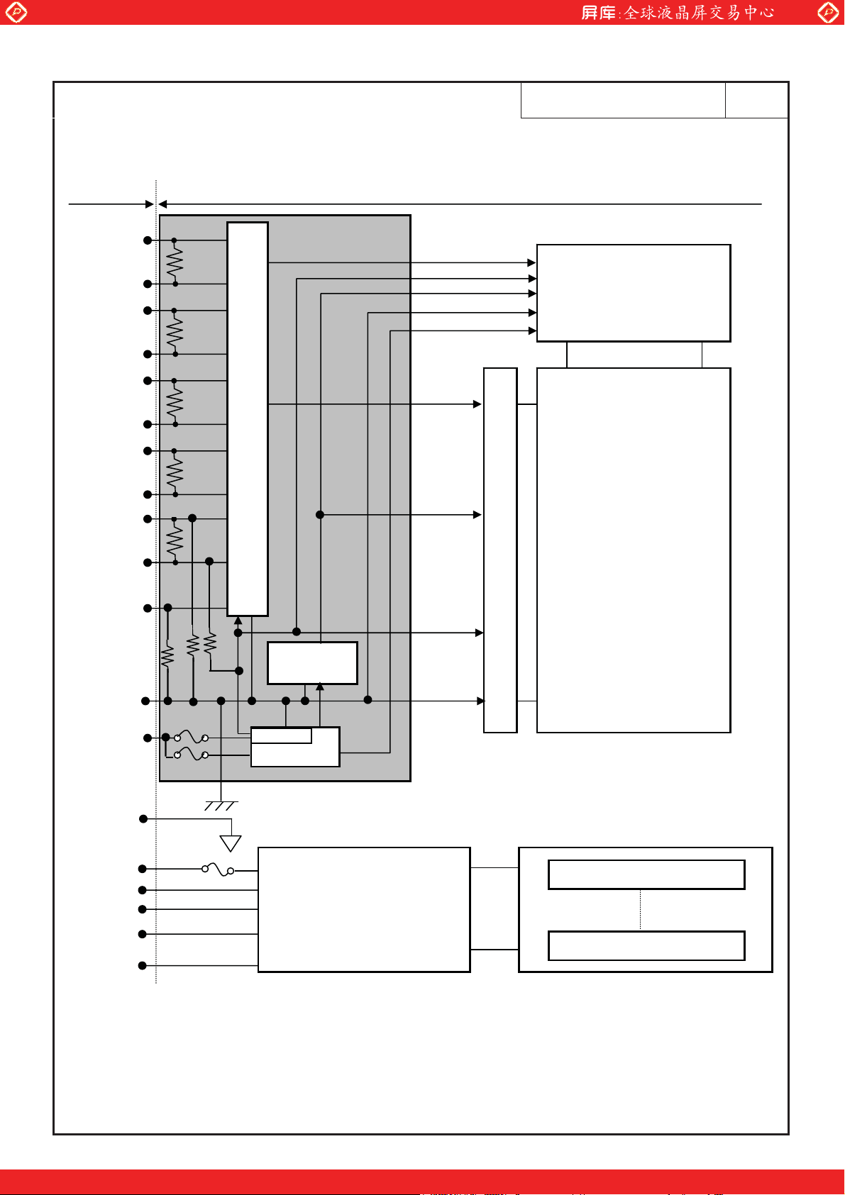
3. BLOCK DIAGRAM
Host LCD Module (Product)
D0+
D0-
D1+
D1-
D2+
D2-
D3+
D3-
CLK+
CLK-
MSL
50 k
GND
Note1 Note2
VCC
FG
Note1
VDDB
BRTC
BRTI
100¡
100¡
100¡
100¡
100¡
2k
5k
Fuse1
Fuse2
Fuse3
V Driver
Power for
scale
DC/DC-1
DC/DC-2
Signal processing board for LCD panel driving
Inverter
SN-SA-A0030-02-E 6/43
H Driver
4,098 columns
LCD Panel
768 rows
H:1,366h3˄R,G,B˅
V:768
Backlight (Direct type)
Lamp #1
BRTP
Lamp # 14
GNDB
Note1: Inside the product, the connection of GND(System ground),FG(Frame ground) and VBLC(Lamp low
voltage terminal), is being discussed.(GND-FG: not connected ,GND-VBLC: not connected ,FG-VBLC:
not connected)
Note2: GND and FG should be connected with the custom equipment’s Ground. Furthermore, it is recommended
that GND,FG and inverter’s Ground in the product should be connected together in customer equipment.
Not duplication without authorization Shanghai SVA NEC Liquid Crystal Display Co., Ltd.
One step solution for LCD / PDP / OLED panel application: Datasheet, inventory and accessory!
www.panelook.com
Global LCD Panel Exchange Center
p
p
www.panelook.com
4. DETAILED SPECIFICATION
4.1 MECHANICAL SPECIFICATIONS
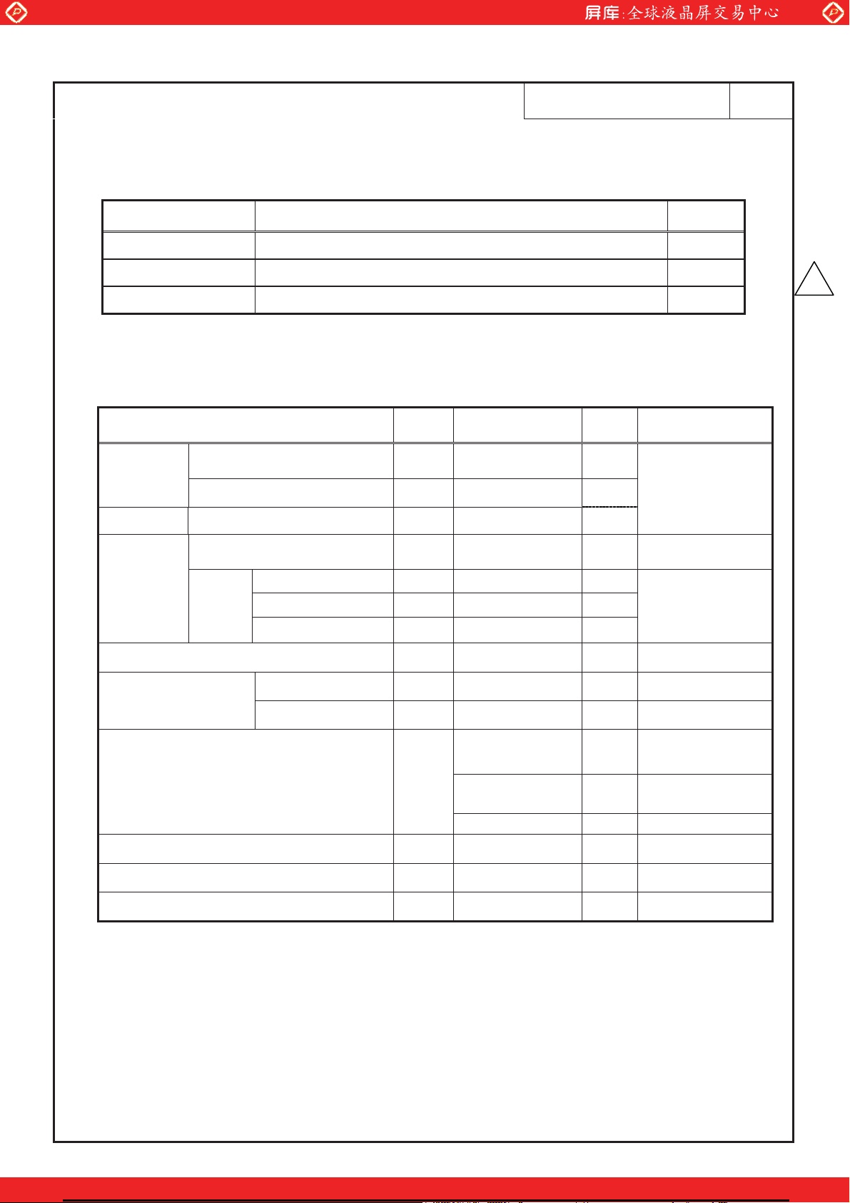
Parameter Specification Unit
Module size 626.0± 1.0 (W) × 373.0± 1.0 (H) × 48.0 (max. , D) Note1,2 mm
Display area 575.77 (W) × 323.71 (H) Note1
Weight (4,800) (typ.) g
Note: See “7. MODULE OUTLINE”.
4.2 ABSOLUTE MAXIMUM RATINGS
Parameter Symbol Rating Unit Remarks
Power supply
voltage
Signal processing board for LCD
anel driving
Backlight VDDB 26.4 Vrms
SN-SA-A0030-02-E 7/43
VCC (Vss-0.5 ~+6.5) V
mm
Ta = 25°C
2
Backlight Lamp current IBL 7.0 mArms
Signal processing board for LCD
anel driving (Note 1)
Input voltage
for signals
Operating temperature
Backlight
inverter
Storage temperature Tst (-20 ~ +65) °C -
Relative humidity Note4 RH
Absolute humidity AH İ g/m3 7D˚°C)
Operating altitude - İˈ m °C˘7Dİ°C)
Storage altitude - İˈ m °C˘7Dİ°C)
Vi (-0.3~ +4.0) V
(BRTC signals) VBC (-0.3~ +6.0) V
(BRTI signals) VBI (-0.3~ +6.0) V
(BRTP signals) VBP (-0.3~ +6.0) V
Front surface TopF (0 ~ +55) °C Note2
Rear surface TopR (0 ~ +65) °C Note3
İ % 7Dİ°C)
İ % °C˘7Dİ°C)
İ % °C˘7Dİ°C)
Ta = 25°C
VDD=5V
Ta = 25 °C
VDD=24V
Note1: Display signals are D0+/-, D1+/-, D2+/-, D3+/-, CK+/-ˈMSL
Note2: Measured at center of LCD panel surface (including self-heat)
Note3: Measured at center of LCD module's rear shield surface (including self-heat)
Note4: No condensation
Not duplication without authorization Shanghai SVA NEC Liquid Crystal Display Co., Ltd.
One step solution for LCD / PDP / OLED panel application: Datasheet, inventory and accessory!
www.panelook.com
Global LCD Panel Exchange Center
www.panelook.com
SN-SA-A0030-02-E 8/43
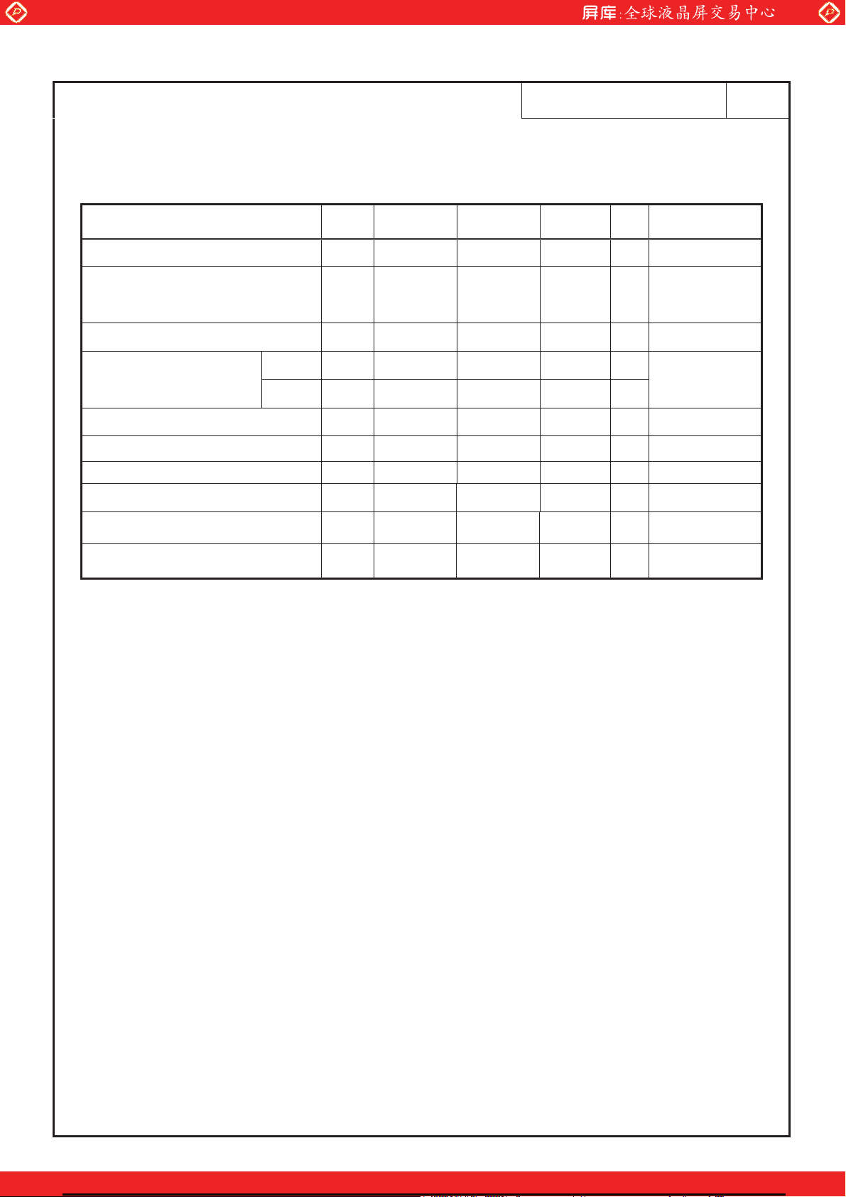
4.3 ELECTRICAL CHARACTERISTICS
4.3.1 Driving for LCD panel signal processing board
Parameter Symbol min. typ. max. Unit Remarks
Power supply voltage VCC (4.5) 5.0 (5.5) V -
Power supply current(Note1)
max value(Note 2)
Permissible ripple voltage VRP - - (100) mV VCC
Differential input threshold
voltage for LVDS receiver
Low VTH - - (+100) mV
High VTL (-100) - - mV
Input voltage width for LVDS receiver Vi (0) - (2.4) V -
Terminal resistor RT - 100 -
Dot clock Oscillation frequency Fdclk (65) (75) (82) MHz
Horizontal Oscillation frequency fh (44) (47) (53) kHz -
ICC -
˄770˅
˄1200˅
mA
(Ta=25°C)
VCC=5.0V
Fv=(60Hz)
Fdclk=(75MHZ)
at VCM =( 1.2V)
Note3
-
-
Vertical Oscillation frequency fv (48) (60) (66) Hz
Rush current Irush - -
Note1: Checked flag pattern
Note2:Sub pixel check pattern(0/255) for theoretical maximum current
Note3: Common mode voltage for LVDS driver
˄1.5˅
A
-
-
Not duplication without authorization Shanghai SVA NEC Liquid Crystal Display Co., Ltd.
One step solution for LCD / PDP / OLED panel application: Datasheet, inventory and accessory!
www.panelook.com
Global LCD Panel Exchange Center
www.panelook.com
SN-SA-A0030-02-E 9/43
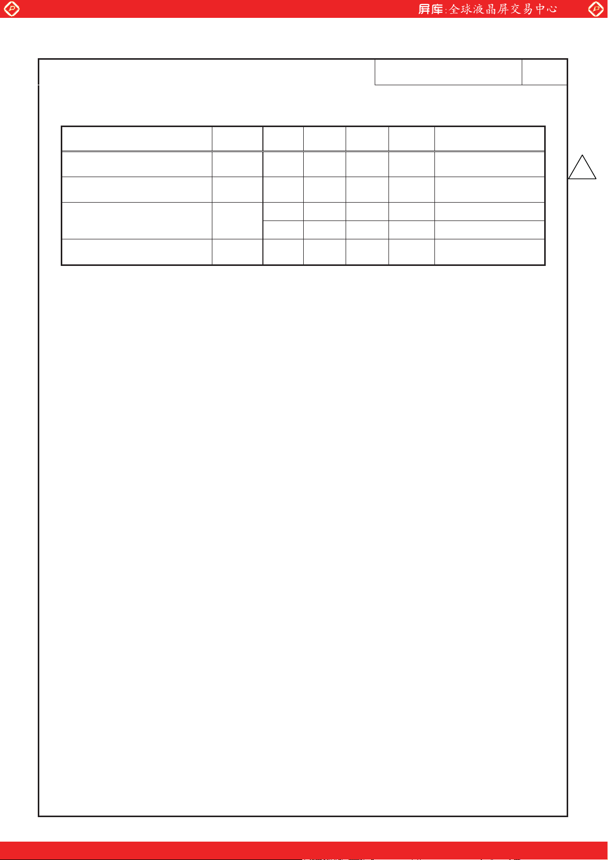
4.3.2 Driving for backlight lamp
Parameter Symbol min. typ. max. Unit Remarks
Lamp current Note3 IBL 4.7 5.2 5.5 mArms
Lamp voltage
Note2,Note3
Lamp starting voltage
Note2,Note3,Note4
Lamp oscillation frequency
Note5
Note: The backlight of this product is made up of 14 piece lamp. The specification above is only for one lamp.
VBLH - (860) - Vrms -
- - 1,500 Vrms Ta = 25ć
VS
- - 1,650 Vrms Ta =0ć
FO 55 60 65 kHz -
(Ta=25°C) Note1
At IDDB=3.3 A
L=(500cd/m
2
)
2
Not duplication without authorization Shanghai SVA NEC Liquid Crystal Display Co., Ltd.
One step solution for LCD / PDP / OLED panel application: Datasheet, inventory and accessory!
www.panelook.com

Global LCD Panel Exchange Center
www.panelook.com
4.3.3 Backlight inverter
Parameter Symbol min. typ. max. Unit Remarks
Power supply voltage VDDB 23.0 24.0 25.0 V
Power supply current *1 IDDB - 3.3 3.8 A
Output current
Open lamp voltage VO 1700 - - V -
(BRTC)
Signal
Control system
input voltage
Control system
input current
*1 The waveform of the current flowing into the inverter is as follows:
Near 5.2(mA)
(BRTI)
Signal
(BRTP)
Signal
(BRTC)
Signal
(BRTI)
Signal
(BRTP)
Signal
High VBCH 2.4 - 5.25 V
Low VBCL 0 - 0.8 V
- VBI 0 - 3.3 V -
High VBPH 2.4 - 5.25 V -
Low VBPL 0 - 0.8 V -
High IBCH - - 1000 A -
Low IBCL -1000 - - A -
- IBI -1000 - 1000 A -
High IBPH - - 3500 A -
Low IBPL -1580 - - A -
IOmax - 5.5 - mArms -
IOmin - 3.0 - mArms -
SN-SA-A0030-02-E 10/43
(Ta=25°C)
-
The maximum
Luminance
at VDDB=24.0V
-
2
Duty: dimming to maximum 100% ~ dimming to minimum 20%, dimming frequency: (180) Hz (TYP.)
In case the noise in the system circuit has occurred, electrolytic capacitor of several kilo F should be
0 (mA)
Duty
Dimming frequency
Note 1: In case the outer pulse dimming is selected, see “
Note 2: During light dimming, big ripple voltage occurs in the power supply line. Ripple voltage will cause audio
noise and signal waveform noise in the system circuit (such as audio circuit) to occur.
assembled between the power lines(VDDB and GNDB).Then the noise can be reduced.
4.6.2 detailed PWM dimming timing”
Not duplication without authorization Shanghai SVA NEC Liquid Crystal Display Co., Ltd.
One step solution for LCD / PDP / OLED panel application: Datasheet, inventory and accessory!
www.panelook.com
Global LCD Panel Exchange Center
(
www.panelook.com
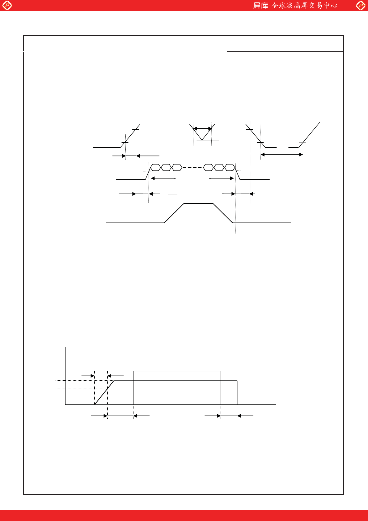
4.4 POWER SUPPLY VOLTAGE SEQUENCE AND RIPPLE
4.4.1 Power supply voltage and B/L control sequence
(t˘20ms) * 1
VA L I D
VCC(Note 1)
0V
Display signal (Note 2)
Function signal
VDDB
ON
(4.5V)
(0.5V)
(0˘Trİ30ms)
90% 90%
0V
(0˘tİ50ms)
SN-SA-A0030-02-E 11/43
(4.5V)
(4.0V)
Toff ˚300ms)
(0˘tİ50ms)
Ć: The signal line is not connected with the module, at the end of cable the terminal resistor of 100 should
be added.
Note 1: In terms of voltage variation (voltage drop) while VCC rising edge is below 4.5V, a protection circuit may
work, and then this product may not work.
Note2: In order not to damage the inner circuit, display signals (D0+/-, D1+/-, D2+/-, D3+/- and CK+/-)must
apply low or high impedance, exclude the VALID period (See above sequence diagram).
If some of display and function signals of this product are cut while this product is working, even if the
signal input to it once again, it might not work normally. If customer stops the display and function signals,
they should cut VCC.
Note3: When VDD is on, it should be set above 4.5V.
Note4: The backlight power supply voltage should be inputted within the valid period of display and function
signals, in order to avoid unstable data display.
4.4.2 Backlight timing
Voltage
BRTC
VDDB
24.0V
23.0V
0˘t 0˘t
Note1: In order to prevent unstable data displaying, inverter’s power supply voltage should be input in the valid
period of LVDS signals.
Note2:If the time for VDDB to start up is over 800ms,inverter’s protection circuit will work, and then backlight
will not be on.
İ800ms
Time
Not duplication without authorization Shanghai SVA NEC Liquid Crystal Display Co., Ltd.
One step solution for LCD / PDP / OLED panel application: Datasheet, inventory and accessory!
www.panelook.com
Global LCD Panel Exchange Center
www.panelook.com
SN-SA-A0030-02-E 12/43
4.4.3 Power supply voltage ripple
When the power supply is designed, the next form can give the reference. If the voltage ripple is over the value in
next form, the noise should be seen in display area.
Ripple (Measured at input terminal of power supply)
Parameter Power supply voltage
VCC 5.0V (İ100) mVp-p
VDDB 24.0V (İ200) mVp-p
Permissible ripple voltage Note 1
(Measured at input terminal of power supply)
Unit
Note 1: Permissible ripple voltage contained spike noise.
4.4.4 Fuse
Parameter
Type Supplier
Fuse1(VCC) FCC16202AB
Fuse
Kamaya electric
Co.Ltd
Rating Fusing current Remarks
2.0A
5A˄~5second˅
32V
Fuse2(VCC) FHC16322AD
Fuse3(VDDB) 25H6300G
Kamaya electric
Co.Ltd
SkyGate Co.,Ltd
Japan
3.15A
24V
6.3A
125V
7.875A
˄~5second˅
12.6A
˄~60second˅
Note 1
Note1: The power supply capacity should be above the fusing current. . If the power supply capacity is less than
the fusing current, the fuse may blow in a short time, and then nasty smell, smoking and so on may occur.
Not duplication without authorization Shanghai SVA NEC Liquid Crystal Display Co., Ltd.
One step solution for LCD / PDP / OLED panel application: Datasheet, inventory and accessory!
www.panelook.com
Global LCD Panel Exchange Center
www.panelook.com
SN-SA-A0030-02-E 13/43
4.5 INTERFACE AND CONNECTOR PIN ALIGNMENT
4.5.1 Connectors for power supply and signals
The rear side of the product
CN1
1 30
Signal processing PWB
1
CN202
4
14
CN201
1
Backlight inverter
Note 1: Connector’s position is not given to correct position as the above drawing shows.
Note 2: Board’s size and shape showed in the above drawing are not the same as the correct image drawings.
Connector inserting direction
Not duplication without authorization Shanghai SVA NEC Liquid Crystal Display Co., Ltd.
One step solution for LCD / PDP / OLED panel application: Datasheet, inventory and accessory!
www.panelook.com
 Loading...