

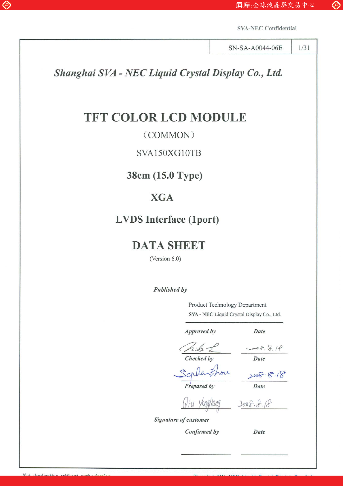
SVA-NEC SVA150XG10TB Specification
Global LCD Panel Exchange Center
Global LCD Panel Exchange Center
www.panelook.com
www.panelook.com
One step solution for LCD / PDP / OLED panel application: Datasheet, inventory and accessory!
One step solution for LCD / PDP / OLED panel application: Datasheet, inventory and accessory!
www.panelook.com
www.panelook.com
Global LCD Panel Exchange Center
Global LCD Panel Exchange Center
www.panelook.com
www.panelook.com
SN-SA-A0044-06E 2/31
INTRODUCTION
• WARRANTY
Shanghai SVA NEC Liquid Crystal Display Co., Ltd. (hereinafter called "SVA-NEC") warrants that this product
meets the product specifications set forth in this document. If this product under normal operation is found to be
non-conforming to the product specifications, and such non-conformance is promptly notified to SVA-NEC within
one (1) year after the delivery date, and further such non-conformance is solely attributable to SVA-NEC, SVA-NEC
shall repair the non-conforming product or replace it with a conforming one, free of charge. However, this warranty
does not apply to any non-conformance that can be found easily by incoming inspections or those resulting from any
one of the following˖
1) Unauthorized or improper repair, maintenance or modification
2) Operation or use against specifications, instructions or warnings given by SVA-NEC
3) Any other causes attributable to customer
In case SVA-NEC repairs or replaces a product after the one (l)-year warranty period, SVA-NEC shall be entitled to
charge for such repair or replacement. Those replaced parts shall be covered with six (6)-month warranty period from
the replacement day. Non-conforming products may be replaced with substitutes instead of repair when the manufacture
of this product has been terminated.
EXCEPT AS EXPRESSLY SET FORTH HEREIN, SVA-NEC DISCLAIMS ANY WARRANTIES,
EXPRESS OR IMPLIED, INCLUDING BUT NOT LIMITED TO MERCHANTABILITY AND FITNESS FOR
A PARTICULAR PURPOSE, AND DISCLAIMS ANY REMEDIES.
• MAINTENANCE
The specifications of maintenance parts may be partially changed within equivalent quality or better. In this
product, SVA-NEC will not accept to maintain for only mounting parts on circuit board (e.g. connector, fuse, capacitor,
resistor, etc.) and only backlight conformation parts (e.g. reflector sheet, light guide plate, etc.).
If SVA-NEC is planning discontinuation for this product, SVA-NEC shall inform it to customers in six (6)-months
advance from the issued date of official agreements. In addition, after product discontinuation, SVA-NEC may replace
substitutes instead of maintenance parts with whole product.
CHANGE CONTROL
•
For the purpose of product improvement, this product design may be changed for specifications, appearance, parts,
circuits and so on. In case a design change is affected on the product specifications, SVA-NEC shall inform it to
customers in advance.
HANDLING OF DOUBTFUL POINTS
•
Any question arising out of, or in connection with, this SPECIFICATION or any matter not stipulated herein will be
settled each time upon consultation between both parties.
Not duplication without authorization Shanghai SVA NEC Liquid Crystal Display Co., Ltd.
One step solution for LCD / PDP / OLED panel application: Datasheet, inventory and accessory!
One step solution for LCD / PDP / OLED panel application: Datasheet, inventory and accessory!
www.panelook.com
www.panelook.com

Global LCD Panel Exchange Center
Global LCD Panel Exchange Center
www.panelook.com
www.panelook.com
SN-SA-A0044-06E 3/31
CONTENTS
INTRODUCTION ....................................................................................................................................................... 2
CONTENTS................................................................................................................................................................. 3
1. OUTLINE ................................................................................................................................................................ 4
1.1 STRUCTURE AND PRINCIPLE.................................................................................................................. 4
1.2 APPLICATIONS ............................................................................................................................................ 4
1.3 FEATURES .................................................................................................................................................... 4
2. GENERAL SPECIFICATIONS ............................................................................................................................... 5
3. BLOCK DIAGRAM ................................................................................................................................................ 6
4. DETAILED SPECIFICATION ................................................................................................................................ 7
4.1 MECHANICAL SPECIFICATIONS ............................................................................................................. 7
4.2 ABSOLUTE MAXIMUM RATINGS............................................................................................................ 7
4.3 ELECTRICAL CHARACTERISTICS.......................................................................................................... 7
4.4 POWER SUPPLY VOLTAGE SEQUENCE.................................................................................................. 9
4.5 CONNECTIONS AND FUNCTIONS FOR INTERFACE PINS ................................................................ 10
4.6 DISPLAY COLORS AND INPUT DATA SIGNALS.................................................................................. 13
4.7 DISPLAY POSITIONS................................................................................................................................ 14
4.8 INPUT SIGNAL TIMINGS FOR LCD PANEL SIGNAL PROCESSING BOARD .................................. 14
4.9 OPTICS........................................................................................................................................................ 17
5. RELIABILITY TESTS .......................................................................................................................................... 19
6. ESTIMATED LUMINANCE LIFETIME ............................................................................................................. 20
7. MARKINGS .......................................................................................................................................................... 21
7.1 PRODUCT LABEL ..................................................................................................................................... 21
7.2 BARCODE LABEL..................................................................................................................................... 21
7.3 OTHER MARKINGS .................................................................................................................................. 21
7.4 INDICATION LOCATIONS ....................................................................................................................... 22
8. PACKING, TRANSPORTATION AND DELIVERY............................................................................................ 23
8.1 PACKING .................................................................................................................................................... 23
8.2 INSPECTION RECORD SHEET................................................................................................................ 23
8.3 TRANSPORTATION ................................................................................................................................... 23
8.4 SIZE AND WEIGHT FOR PACKING BOX ............................................................................................... 23
8.5 OUTLINE FIGURE FOR PACKING.......................................................................................................... 24
9. PRECAUTIONS .................................................................................................................................................... 26
9.1 MEANING OF CUTION SIGNS ................................................................................................................ 26
2 CAUTIONS ............................................................................................................................................... 26
9.
9.3 ATTENTIONS ............................................................................................................................................. 26
10.OUTDRAWING ................................................................................................................................................... 28
Not duplication without authorization Shanghai SVA NEC Liquid Crystal Display Co., Ltd.
One step solution for LCD / PDP / OLED panel application: Datasheet, inventory and accessory!
One step solution for LCD / PDP / OLED panel application: Datasheet, inventory and accessory!
www.panelook.com
www.panelook.com
Global LCD Panel Exchange Center
Global LCD Panel Exchange Center
www.panelook.com
www.panelook.com
SN-SA-A0044-06E 4/31
1. OUTLINE
1.1 STRUCTURE AND PRINCIPLE
SVA150XG10TB module is composed of the amorphous silicon thin film transistor liquid crystal display (a-Si
TFT LCD) panel structure with driver LSIs for driving the TFT (Thin Film Transistor) array and a backlight.
The a-Si TFT LCD panel structure is injected liquid crystal material into a narrow gap between the TFT array
glass substrate and a color-filter glass substrate.
Color (Red, Green, Blue) data signals from a host system (e.g. PC, signal generator, etc.) are modulated into best
form for active matrix system by a signal processing board, and sent to the driver LSIs which drive the individual
TFT arrays.
The TFT array as an electro-optical switch regulates the amount of transmitted light from the backlight assembly,
when it is controlled by data signals. Color images are created by regulating the amount of transmitted light through
the TFT array of red, green and blue dots.
1.2 APPLICATIONS
• Monitor for PC
1.3 FEATURES
• a-Si TFT active matrix
• LVDS interface (6 bit+FRC)
• Wide viewing angle
• high response time : 8ms (typ.)
• PSWG standard
• High contrast: 600:1(typ.)
• Edge light type backlight (Inverter less)
• RoHS compliance
• TCO’03 compliance
6
Not duplication without authorization Shanghai SVA NEC Liquid Crystal Display Co., Ltd.
One step solution for LCD / PDP / OLED panel application: Datasheet, inventory and accessory!
One step solution for LCD / PDP / OLED panel application: Datasheet, inventory and accessory!
www.panelook.com
www.panelook.com
Global LCD Panel Exchange Center
Global LCD Panel Exchange Center
www.panelook.com
www.panelook.com
2. GENERAL SPECIFICATIONS
Display area
Diagonal size of display
Drive system
Display color
Pixel
Pixel arrangement
Dot pitch
Pixel pitch
Module size
Weigh t
Contrast ratio
304.128 (W) x 228.096 (H) mm (typ.)
38.0 cm (15.0 inches)
a-Si TFT active matrix
16,777,216 colors (6bit+FRC)
1,024 (H) x 768 (V) pixels
RGB (Red dotǃGreen dotǃ Blue dot) vertical stripe
0.099 (W) x 0.297 (H) mm
0.297 (W) x 0.297 (H) mm
326.50f0.5 (W) x 253.5f0.5 (H) x 11.13f0.5 (D) mm (typ.)
1000 g (typ.)
600:1 (typ.)
SN-SA-A0044-06E 5/31
Viewing angle
(At the contrast ratio 10
Designed viewing direction
Color gamut
Response time
Luminance
Transmissive Mode
Surface Treatment
Signal system
Power supply voltage
Backlight
Power consumption
˖
1)
• Horizontal: 160° (typ.)
• Vertical: 160° (typ.)
• Viewing angle with optimum grayscale (¤=2.2): normal axis
At LCD panel center
60 % (typ.) [against NTSC color space]
Ton (white 90% black 10%) + Toff (black 10% white 90%)
8 ms (typ.)
At IBL = 7mArms / lamp
250cd/m
Normally White
AG Type
LVDS 1port
LCD panel signal processing board˖3.3V
Edge light type˖2 cold cathode fluorescent lamps
At IBL=7mArms / lamp and checkered flag pattern
(10.1 )W (typ.)
2
(typ.)
[ RGB :8-bit, Dot clock (CLK), Data enable (DE)]
6
Not duplication without authorization Shanghai SVA NEC Liquid Crystal Display Co., Ltd.
One step solution for LCD / PDP / OLED panel application: Datasheet, inventory and accessory!
One step solution for LCD / PDP / OLED panel application: Datasheet, inventory and accessory!
www.panelook.com
www.panelook.com
Global LCD Panel Exchange Center
Global LCD Panel Exchange Center
www.panelook.com
www.panelook.com
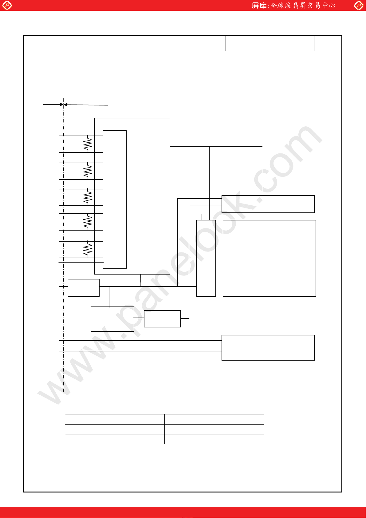
3. BLOCK DIAGRAM
LCD MODULE I/F
D0-
D0+
D1-
D1+
D2-
D2+
CLK-
CLK+
D3-
D3+
MSL
VCC
VBLH1/2
VBLC2/2
100¡
100¡
100¡
100¡
100¡
FUSE
DC/DC
converter
NT71660(NOVATEK)
SN-SA-A0044-06E 6/31
VKOKPIEQPVTQNNGTKPENWFKPI.8&5
Source Driver
3072 columns
Gate Driver
Power
LCD Panel
768 rows
H:1024h3˄R,G,B˅
V:768
Edge side backlight
Note1: Connections between GND, FG (Frame ground) and VBLC (Lamp low voltage terminal) in the product
GND - FG Connected
GND - VBLC Not connected
FG - VBLC Not connected
Note2: These grounds should be connected together in customer equipment.
Not duplication without authorization Shanghai SVA NEC Liquid Crystal Display Co., Ltd.
One step solution for LCD / PDP / OLED panel application: Datasheet, inventory and accessory!
One step solution for LCD / PDP / OLED panel application: Datasheet, inventory and accessory!
www.panelook.com
www.panelook.com
Global LCD Panel Exchange Center
Global LCD Panel Exchange Center
www.panelook.com
www.panelook.com
4. DETAILED SPECIFICATION
4.1 MECHANICAL SPECIFICATIONS
Parameter Specification Unit
Module size 326.5f0.5 (W) x 253.5f0.5 (H) x 11.13f0.5 (D) Note1 mm
Display area 304.128 (W) x 228.096 (H) Note1 mm
Weight 1000 (typ.) g
Note1: See “10. OUTLINE DRAWINGS”.
4.2 ABSOLUTE MAXIMUM RATINGS
SN-SA-A0044-06E 7/31
Parameter Symbol Rating Unit Remarks
Power supply
voltage
Input voltage
for signals
Operating temperature
Note1: Display signals are D0+/-, D1+/-, D2+/-, D3+/- and CK+/-.
Note2: Function signal is MSL.
Note3: Measured at center of LCD panel surface (including self-heat)
Note4: Measured at center of LCD module’s rear shield surface (including self-heat)
Note5: No condensation
Note6: Ta = 50ć, RH = 85%
LCD panel signal board VCC -0.3 to +3.6 V Ta = 25ć
Display signals
Note1
Function signals
Note2
Storage temperature Tst -20 to +60 ć -
Front surface TopF 0 to +50 ć Note3
Rear surface TopR 0 to +55 ć Note4
Relative humidity
Note5
Absolute humidity
Note6
Vi
RH
AH
-0.3 to +3.6
and
Vi<VCC +0.3
95 % Ta 40ć
85 % 40 <Ta 50ć
70
Note6
V Ta = 25ć
3
Ta > 50ć
g/m
Not duplication without authorization Shanghai SVA NEC Liquid Crystal Display Co., Ltd.
One step solution for LCD / PDP / OLED panel application: Datasheet, inventory and accessory!
One step solution for LCD / PDP / OLED panel application: Datasheet, inventory and accessory!
www.panelook.com
www.panelook.com
Global LCD Panel Exchange Center
Global LCD Panel Exchange Center
www.panelook.com
www.panelook.com
SN-SA-A0044-06E 8/31
4.3 ELECTRICAL CHARACTERISTICS
4.3.1 Driving for LCD panel signal processing board
Parameter Symbol min. typ. max. Unit Remarks
Power supply voltage VCC 3.0 3.3 3.6 V Power supply current ICC - (500)1 (700)2 mA at VCC = 3.3V
Permissible ripple voltage VRP - - 100 mV For VCC
Differential input threshold
voltage for LVDS receiver
Input voltage width for LVDS receiver Vi 0 - 2.4 V -
Terminating resistor RT - 100 - -
Input voltage for MSL signal
1: Checkered flag pattern (EIAJ ED-2522)2: 2H1V dot inverse pattern
3: Common mode voltage for LVDS receiver
Low VTL -100 - mV
High VTH - - 100 mV
Low VFL 0 - 0.8 V
High VFH 2.0 - VCC V
at VCM = 1.2V
4.3.2 Driving for backlight lamp
Note3
-
Parameter Symbol min. typ. max. Unit Remarks
Lamp current +N 3.5 7.0 7.5 mArms at L = 250cd/ m2 (typ.)
Lamp voltage Vl 549 610 671 Vrms For each lamp
Note1
Oscillation frequency FO 40 50 60 kHz Note3
Note1: The value is the characteristic of lamp. The starting voltage of inverter should be lower than the value. But
the possibility of not lighting exists by the lower voltage, so the suitable voltage should considered by the
test .
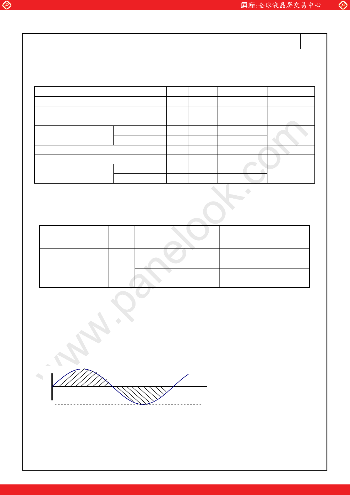
Note2: The asymmetric ratio of working waveform for lamps (Lamp voltage peak ratio, Lamp current peak ratio
and waveform space ratio) should be less than 5% (See the following figure). If the waveform is asymmetric, DC
(Direct current) element applies into the lamp. In this case, a lamp lifetime may be shortened, because a
distribution of a lamp enclosure substance inclines toward one side between low voltage terminal (Cold terminal)
and high voltage terminal (Hot terminal).
Pa
Sa
VS
- - 1600 Vrms Ta = 0ć Note2 Lamp starting voltage
- - 1100 Vrms Ta = 25ć Note2
|Pa - Pb| / Pb × 100 İ 5%
|Sa - Sb| / Sb × 100 İ 5%
Sb
Pb
Supply voltage/current peak for positive, Pb: Supply voltage/current peak for negative
Pa:
Sa: Waveform space for positive part, Sb: Waveform space for negative part
Note3: Recommended value of “FO” is as following.
FO = 1/4 x 1/th x (2n-1) n: Natural number (1, 2, 3 ……)
Not duplication without authorization Shanghai SVA NEC Liquid Crystal Display Co., Ltd.
One step solution for LCD / PDP / OLED panel application: Datasheet, inventory and accessory!
One step solution for LCD / PDP / OLED panel application: Datasheet, inventory and accessory!
www.panelook.com
www.panelook.com
Global LCD Panel Exchange Center
Global LCD Panel Exchange Center
www.panelook.com
www.panelook.com
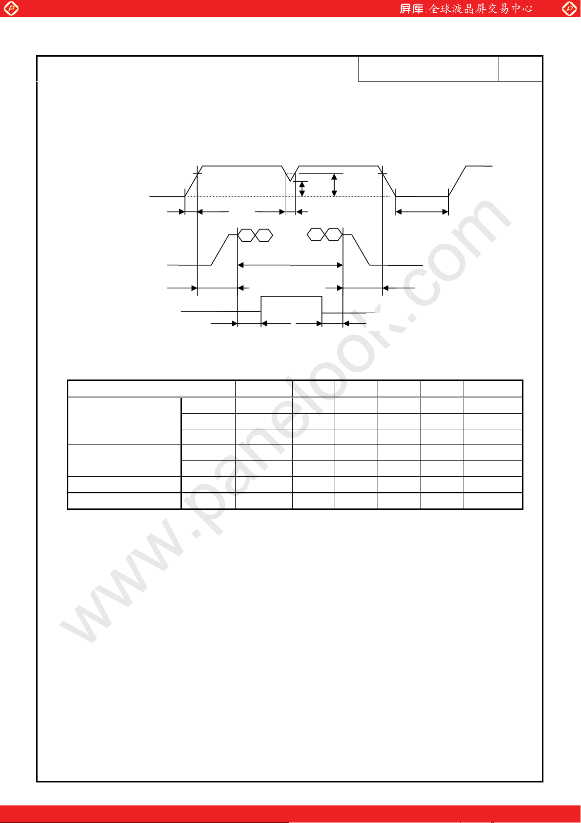
4.4 POWER SUPPLY VOLTAGE SEQUENCE
4.4.1 The sequence of backlight and power supply
VCC ON VCC OFF
3.0 V
VCC
Note1
Display signals*
Function signal*
Note2
* These signals should be measured at the terminal of 100 resistor.
0 V
0 V
Backlight
signal
Parameter Symbol min. typ. max. Unit Remarks
A
D C
VALID period
2.5 V
SN-SA-A0044-06E 9/31
3.0 V
FE
ON A - - 10 ms -
Input voltage sequence
signal sequence
B/L igniting ON G 200 - - ms PSWG
B/L extinguishing OFF H 200 - - ms -
: VCC should be 2.5 V or more while VCC ON period.
[NOTE ITEM]
Note1: In terms of voltage variation (voltage drop) while VCC rising edge is below 3.0 V, a protection circuit
may work, and then this product may not work.
Note2: Display signals (D0+/-, D1+/-, D2+/-, D3+/- and CK+/-) and function signal (MSL) must be “0” voltage,
exclude the VALID period (See above sequence diagram). If these signals are higher than 0.3 V, the
internal circuit is damaged.
If some of display and function signals of this product are cut while this product is working, even if the
signal input to it once again, it might not work normally. If customer stops the display and function
signals, they should be cut VCC.
Note3: The backlight power supply voltage should be inputted within the valid period of display and function
signals, in order to avoid unstable data display.
Note4: In order to prevent unstable data displaying, suggest that, during display and function signal’s valid
period, backlight power voltage should be input under the custom ’ condition as possible.
Moment C 500 - - ms -
DIP D - - 20 ms
ON E 0.01 - 50 ms - Power supply and
OFF F 0.01 - 50 ms -
4.4.2 Power supply voltage ripple
This product works, even if the ripple voltage levels are beyond the permissible values as the following table,
but there might be noise on the display image.
Not duplication without authorization Shanghai SVA NEC Liquid Crystal Display Co., Ltd.
One step solution for LCD / PDP / OLED panel application: Datasheet, inventory and accessory!
One step solution for LCD / PDP / OLED panel application: Datasheet, inventory and accessory!
www.panelook.com
www.panelook.com
Global LCD Panel Exchange Center
Global LCD Panel Exchange Center
www.panelook.com
www.panelook.com
Parameter Power supply voltage
VCC 3.3 V 100 mVp-p
(Measured at input terminal of power supply)
Ripple voltage Note1
SN-SA-A0044-06E 10/31
Unit
Note1: The permissible ripple voltage includes spike noise.
4.4.3 Fuse
Parameter
Type Supplier
VCC TF16SN2.50 KOA Corporation
Fuse
Rating Fusing current Remarks
1.5 A
5.0 A Note1
32 V
Note1: The power supply capacity should be more than the fusing current. If the power supply capacity is less than
the fusing current, the fuse may not blow for a short time, and then nasty smell, smoking and so on may occur.
4.5 CONNECTIONS AND FUNCTIONS FOR INTERFACE PINS
4.5.1 LCD panel signal processing board
CN1 socket(Module side): DF-14H-20P-1.25H˄Hirose Electric Co., Ltd.˅
Adaptable plug˖ DF14-20S-1.25C˄Hirose Electric Co., Ltd.˅
Pin No. Symbol Signal Remarks
1 VCC
2 VCC
3 GND
4 GND
5 D0-
6 D0+
7 GND Ground -
8 D1-
9 D1+
10 GND Ground -
11 D2-
12 D2+
13 GND Ground -
14 CLK-
15 CLK+
Power supply -
Ground -
Pixel data Note2
Pixel data Note2
Pixel data Note2
Pixel clock Note2
16 GND Ground -
17 D3-
Pixel data Note2
18 D3+
19 GND Ground -
20 MSL
Not duplication without authorization Shanghai SVA NEC Liquid Crystal Display Co., Ltd.
One step solution for LCD / PDP / OLED panel application: Datasheet, inventory and accessory!
One step solution for LCD / PDP / OLED panel application: Datasheet, inventory and accessory!
Selection of LVDS input
Map
Low or Open: NOTE1
www.panelook.com
www.panelook.com
 Loading...