

Page 1
Global LCD Panel Exchange Center
www.panelook.com
Shanghai SVA NEC Liquid Crystal Display Co., Ltd.
TFT COLOR LCD MODULE
SVA150XG01TB
38cm (15.0 Type)
XGA
LVDS Interface (1port)
SN-SA-A0001-01-E 1/38
PRELIMINARY DATA SHEET
(1st edition)
Signature of writer
approved by Date
checked by Date
Prepared by Date
L
L
L
Published by
Technology Department
SVA NEC Liquid Crystal Display Co., Ltd.
Shanghai SVA NEC Liquid Crystal Display Co., Ltd.
One step solution for LCD / PDP / OLED panel application: Datasheet, inventory and accessory!
www.panelook.com
Page 2
Global LCD Panel Exchange Center
www.panelook.com
SN-SA-A0001-01-E 2/38
INTRODUCTION
• WARRANTY
Shanghai SVA NEC Liquid Crystal Display Co., Ltd. (hereinafter called "SVA-NEC") warrants that this product
meets the product specifications set forth in this document. If this product under normal operation is found to be
non-conforming to the product specifications, and such non-conformance is promptly notified to SVA-NEC within
one (1) year after the delivery date, and further such non-conformance is solely attributable to SVA-NEC, SVA-NEC
shall repair the non-conforming product or replace it with a conforming one, free of charge. However, this warranty
does not apply to any non-conformance that can be found easily by incoming inspections or those resulting from any
one of the following˖
1) Unauthorized or improper repair, maintenance or modification
2) Operation or use against specifications, instructions or warnings given by SVA-NEC
3) Any other causes attributable to customer
In case SVA-NEC repairs or replaces a product after the one (l)-year warranty period, SVA-NEC shall be entitled to
charge for such repair or replacement. Those replaced parts shall be covered with six (6)-month warranty period from
the replacement day. Non-conforming products may be replaced with substitutes instead of repair when the manufacture
of this product has been terminated.
EXCEPT AS EXPRESSLY SET FORTH HEREIN, SVA-NEC DISCLAIMS ANY WARRANTIES,
EXPRESS OR IMPLIED, INCLUDING BUT NOT LIMITED TO MERCHANTABILITY AND FITNESS FOR
A PARTICULAR PURPOSE, AND DISCLAIMS ANY REMEDIES.
• MAINTENANCE
The specifications of maintenance parts may be partially changed within equivalent quality or better. In this
product, SVA-NEC will not accept to maintain for only mounting parts on circuit board (e.g. connector, fuse, capacitor,
resister, etc.) and only backlight conformation parts (e.g. reflector sheet, light guide plate, etc.).
If SVA-NEC is planning discontinuation for this product, SVA-NEC shall inform it to customers in six (6)-months
advance from the issued date of official agreements. In addition, after product discontinuation, SVA-NEC may replace
substitutes instead of maintenance parts with whole product.
CHANGE CONTROL
•
For the purpose of product improvement, this product design may be changed for specifications, appearance, parts,
circuits and so on. In case a design change is affected on the product specifications, SVA-NEC shall inform it to
customers in advance.
HANDLING OF DOUBTFUL POINTS
•
Any question arising out of, or in connection with, this SPECIFICATION or any matter not stipulated herein will be
settled each time upon consultation between both parties.
Shanghai SVA NEC Liquid Crystal Display Co., Ltd.
One step solution for LCD / PDP / OLED panel application: Datasheet, inventory and accessory!
www.panelook.com
Page 3
Global LCD Panel Exchange Center
www.panelook.com
SN-SA-A0001-01-E 3/38
CONTENTS
INTRODUCTION...................................................................................................................................................2
1. OUTLINE .............................................................................................................................................................5
1.1 STRUCTURE AND PRINCIPLES.....................................................................................................................5
1.2 APPLICATIONS...............................................................................................................................................5
1.3 FEATURES.......................................................................................................................................................5
2. GENERAL SPECIFICATIONS..........................................................................................................................6
3. BLOCK DIAGRAM.............................................................................................................................................7
4. DETAILED SPECIFICATIONS.........................................................................................................................8
4.1 MECHANICAL SPECIFICATIONS ..............................................................................................................8
4.2 ABSOLUTE MAXIMUM RATINGS..............................................................................................................8
4.3 ELECTRICAL CHARACTERISTICS.............................................................................................................9
4.3.1 Driving for LCD panel signal processing board......................................................................................9
4.3.2 Driving for backlight lamp.....................................................................................................................10
4.3.3 Power supply voltage ripple...................................................................................................................11
4.3.4 Fuse.................. ......................................................................................................................................11
4.4 POWER SUPPLY VOLTAGE SEQUENCE................................................................................................. .12
4.5 CONNECTIONS AND FUNCTIONS FOR INTERFACE PINS...................................................................13
4.5.1 LCD panel signal processing board........................................................................................................13
4.5.2 Backlight lamp........................................................................................................................................14
4.5.3 Positions of plugs and a socket...............................................................................................................14
4.5.4 Connection between receiver and transmitter for LVDS........................................................................15
4.6 DISPLAY COLORS AND INPUT DATA SIGNALS ....................................................................................17
4.7 DISPLAY POSITONS..............................................................................
4.8 SCANNING DIRECTIONS............................................................................................................................18
4.9 INPUT SIGNAL TIMINGS FOR LCD PANEL SIGNAL PROCESSING BOARD.....................................19
4.9.1 Outline of input signal timings...............................................................................................................19
4.9.2 Timing characteristics.............................................................................................................................20
4.9.3 Input signal timing chart.........................................................................................................................21
4.10 OPTICS..........................................................................................................................................................22
4.10.1 Optical characteristics.......................................................................................................................... 22
4.10.2 Definition of contrast ratio....................................................................................................................23
4.10.3 Definition of luminance uniformity......................................................................................................23
4.10.4 Definition of response times ................................................................................................................23
4.10.5 Definition of viewing angles.................................................................................................................23
.......................................................18
4.11 DEFECT CRITERIA..................................................................................................................................... 24
4.11.1 Display specifications............................................................................................................................24
4.11.2 Close defect dots....................................................................................................................................25
4.11.3 Linked defect dots..................................................................................................................................25
4.11.4 Appearance specifications......................................................................................................................27
Shanghai SVA NEC Liquid Crystal Display Co., Ltd.
One step solution for LCD / PDP / OLED panel application: Datasheet, inventory and accessory!
www.panelook.com
Page 4
Global LCD Panel Exchange Center
www.panelook.com
SN-SA-A0001-01-E 4/38
CONTENTS
5. ESTIMATED LUMINANCE LIFETIME..........................................................................................................28
6. PRODUCT INSPECTIONS ............................................................................................................................... 28
7. RELIABILITY TESTS........................................................................................................................................ 29
8. MARKINGS ......................................................................................................................................................... 30
8.1 NAMEPLATE LABEL.....................................................................................................................................30
8.2 BARCODE LABEL..........................................................................................................................................30
8.3 OTHER MARKINGS.......................................................................................................................................30
8.4 INDICATION LOCATIONS ............................................................................................................................31
9. PACKING, TRANSPORTATION AND DELIVERY.........................................................................................32
9.1 PACKING......................................................................................................................................................... 32
9.2 INSPECTION RECORD SHEET..................................................................................................................... 32
9.3 TRANSPORTATION........................................................................................................................................ 32
9.4 SIZE AND WEIGHT FOR PACKING BOX.................................................................................................... 32
9.5 OUTLINE FIGURE FOR PACKING............................................................................................................... 33
10. PRECAUTIONS...................................................................................................................................................35
10.1 MEANING OF CAUTION SIGNS.................................................................................................................35
2 CAUTIONS.....................................................................................................................................................35
10.
10.3 ATTENTIONS.................................................................................................................................................35
10.3.1 Handling of the product..........................................................................................................................35
10.3.2 Environment............................................................................................................................................36
10.3.3 Characteristics.........................................................................................................................................36
10.3.4 Other.......................................................................................................................................................36
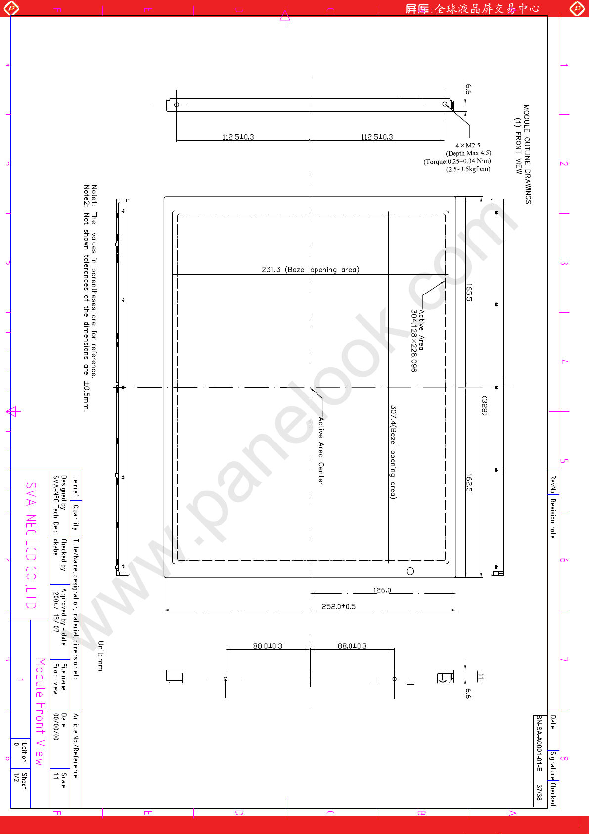
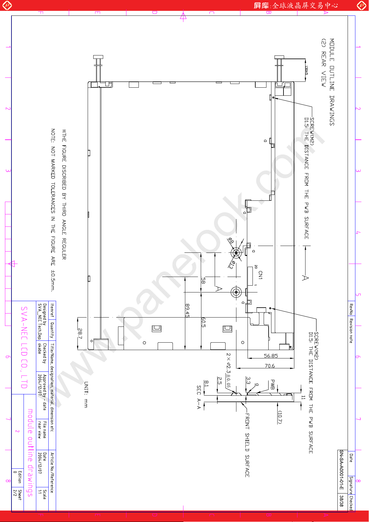
11. OUTLINE DRAWINGS......................................................................................................................................37
11.1 FRONT VIEW...................................................................................................................................................37
11.2 REAR VIEW.....................................................................................................................................................38
Shanghai SVA NEC Liquid Crystal Display Co., Ltd.
One step solution for LCD / PDP / OLED panel application: Datasheet, inventory and accessory!
www.panelook.com
Page 5
Global LCD Panel Exchange Center
www.panelook.com
SN-SA-A0001-01-E 5/38
1. OUTLINE
1.1 STRUCTURE AND PRINCIPLE
A150XG01TB module is composed of the amorphous silicon thin film transistor liquid crystal display (a-Si
SV
TFT LCD) panel structure with driver LSIs for driving the TFT (Thin Film Transistor) array and a backlight.
The a-Si TFT LCD panel structure is injected liquid crystal material into a narrow gap between the TFT array
glass substrate and a color-filter glass substrate.
Color (Red, Green, Blue) data signals from a host system (e.g. PC, signal generator, etc.) are modulated into best
form for active matrix system by a signal processing board, and sent to the driver LSIs which drive the individual
TFT arrays.
The TFT array as an electro-optical switch regulates the amount of transmitted light from the backlight assembly,
when it is controlled by data signals. Color images are created by regulating the amount of transmitted light through
the TFT array of red, green and blue dots.
1.2 APPLICATIONS
• Monitor for PC
1.3 FEATURES
VDS interface (8 bit)
• L
• Selectable LVDS input map
• Wide color gamut
• High contrast
• Edge light type backlight (Inverter less)
• Replaceable lamp for backlight
Shanghai SVA NEC Liquid Crystal Display Co., Ltd.
One step solution for LCD / PDP / OLED panel application: Datasheet, inventory and accessory!
www.panelook.com
Page 6
Global LCD Panel Exchange Center
www.panelook.com
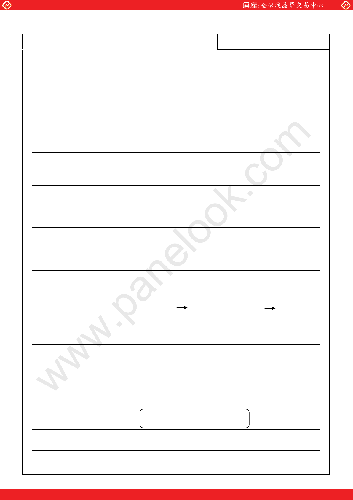
2. GENERAL SPECIFICATIONS
Display area
Diagonal size of display
Drive system
Display color
Pixel
Pixel arrangement
itch
Dot p
Pixel pitch
Module size
Weight
Contrast ratio
Viewing angle
304.128 (W) x 228.096 (H) mm (typ.)
38.0 cm (15.0 inches)
a-Si TFT active matrix
16,777,216 colors (6bit+FRC)
1,024 (H) x 768 (V) pixels
RGB (Red dotǃGreen dotǃ Blue dot) vertical stripe
0.099 (W) x 0.297 (H) mm
0.297 (W) x 0.297 (H) mm
328.0 (W) x 252.0 (H) x 11.0 (D) mm (typ.)
970 g (typ.)
400:1 (typ.)
At the contrast ratio 10
• Horizontal: Right side 60° (typ.). Left side 60° (typ.)
˖
SN-SA-A0001-01-E 6/38
1
Designed viewing direction
Polarizer surface
Polarizer pencil-hardness
Color gamut
Response time
Luminance
Signal system
Power supply voltage
• Vertical: Up side 40° (typ.). Down side 60° (typ.)
• Viewing direction without image reversal: up side (12 o'clock)
• Viewing direction with contrast peak: down side (6 o'clock)
• Viewing angle with optimum grayscale (¤=2.2): normal axis
Antiglare
3H (min.) [by JIS K5400]
At LCD panel center
60 % (typ.) [against NTSC color space]
Ton (white 90% black 10%) + Toff (black 10% whjte 90%)
25 ms (typ.)
At IBL = 7.5mArms / lamp
2
250cd/m
LVDS 1port (Receiver: Equivalent of THC63LVDF84A, THine
Electronics Inc.)
LCD panel signal processing board˖3.3V
(typ.)
[8-bit digital signals for data of RGB colors, Dot clock (CLK),
Data enable (DE)]
Edge light type˖2 cold cathode fluorescent lamps
Backlight
consumption
Power
Replaceable part
• Lamp holder set˖Type No. 150LHS21
At IBL=7.5mArms / lamp and checkered flag pattern
9.4W (typ.)
Shanghai SVA NEC Liquid Crystal Display Co., Ltd.
One step solution for LCD / PDP / OLED panel application: Datasheet, inventory and accessory!
www.panelook.com
Page 7
Global LCD Panel Exchange Center
)
www.panelook.com
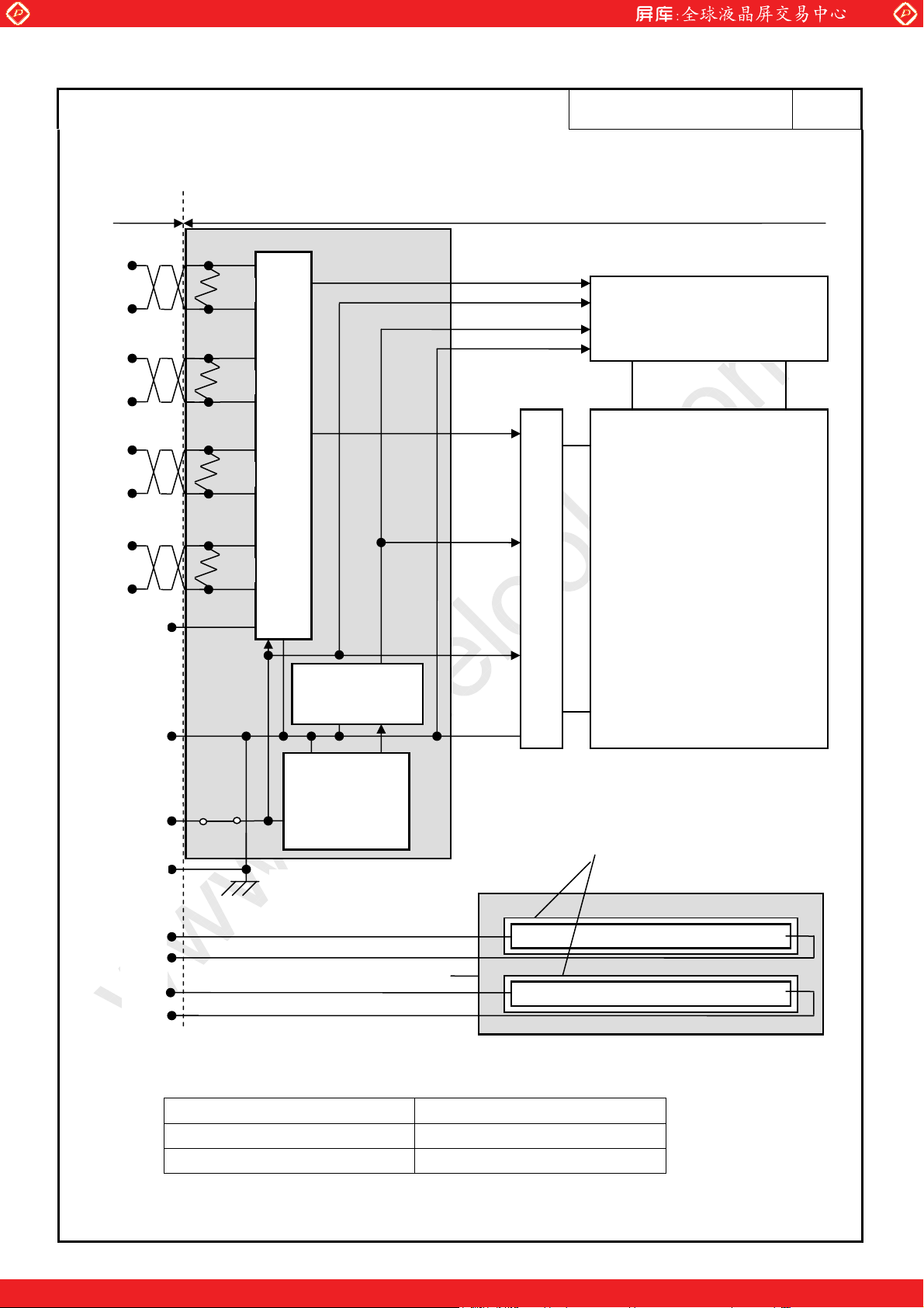
3. BLOCK DIAGRAM
Host
D0+
D0
D1+
D1
D2+
D2-
CK+
-
-
LCD module (Product
100
100
100
SN-SA-A0001-01-E 7/38
H - driver
3,072 lines
LCD panel
CK-
MSL
GND
Note1
Note2
VCC
FG
Note1
Note2
VBLH
VBLC
Note1
VBLH
VBLC
Note1
100
+3.
Fuse
Controller with receiver for LVDS
3V
Power supply
For gradation
DC/DC
converter
LCD panel signal processing board
Backlight (Edge light type)
V - driver
Meta
llic frame of lamp holder
H: 1,024 x 3 (R, G, B)
V: 768
768 lines
Lamp
Lamp
Note1: Connections between GND, FG (Frame ground) and VBLC (Lamp low voltage terminal) in
the product
GND - FG Connected
GND - VBLC Not connected
FG - VBLC Not connected
Note2: These grounds should be connected together in customer equipment.
Shanghai SVA NEC Liquid Crystal Display Co., Ltd.
One step solution for LCD / PDP / OLED panel application: Datasheet, inventory and accessory!
www.panelook.com
Page 8
Global LCD Panel Exchange Center
www.panelook.com
4. DETAILED SPECIFICATIONS
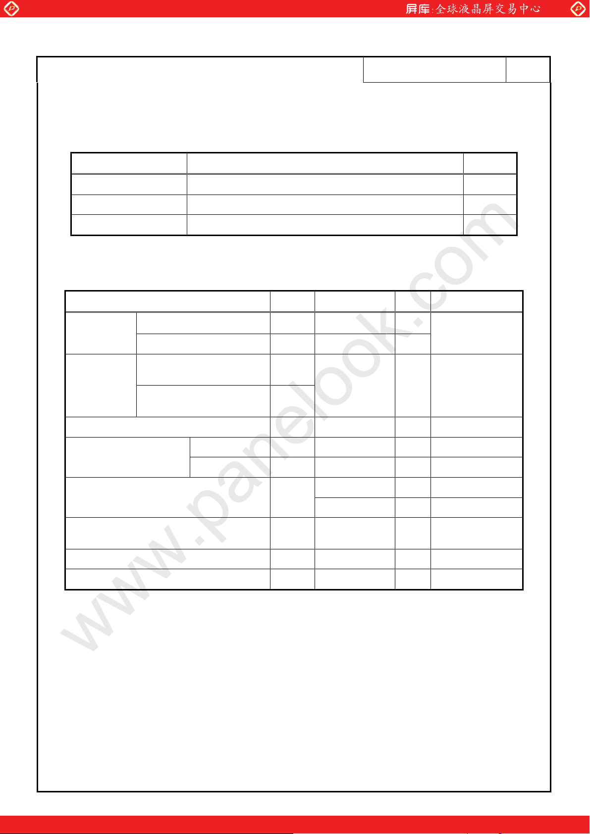
4.1 MECHANICAL SPECIFICATIONS
meter Specification Unit
Para
Module size 328.0 ± 0.5 (W) x 252.0 ± 0.5 (H) x 11.0 ± 0.5 (D) Note1 mm
Display area 304.128 (W) x 228.096 (H) Note1 mm
Weight 970 (typ.), 1050 (max.) g
Note1: See “11. OUTLINE DRAWINGS”.
4.2 ABSOLUTE MAXIMUM RATINGS
Parameter Symbol Rating Unit Remarks
Powe supply
voltage
LCD panel signal board VCC -0.3 to +3.6 V
Lamp voltage VBLH 2000 Vrms
SN-SA-A0001-01-E 8/38
Ta = 25ć
Input voltage
for signals
torage temperature Tst -20 to +60 ć -
S
Operating temperature
Relative humidity
Absolute humidity
Operating altitude - 4,850 m 0ć Ta 50ć
Storage altitude - 13,600 m -20ć Ta 60ć
Display signals
Note1
Function signals
Note2
Front surface TopF 0 to +50 ć Note3
Rear surface TopR 0 to +55 ć Note4
Note5
Note6
VD
VF
RH
AH
-0.3 to +3.6
and
<VCC +0.3
95 % T
85 % 40 <Ta 50ć
70
Note6
VTa = 25ć
g/m
3
Ta > 50ć
Note1: Display signals are D0+/-, D1+/-, D2+/-, D3+/- and CK+/-.
Note2: Function signal is MSL.
Note3: Measured at center of LCD panel surface (including self-heat)
Note4: Measured at center of LCD module’s rear shield surface (including self-heat)
Note5: No condensation
Note6: Ta = 50ć, RH = 85%
a 40ć
Shanghai SVA NEC Liquid Crystal Display Co., Ltd.
One step solution for LCD / PDP / OLED panel application: Datasheet, inventory and accessory!
www.panelook.com
Page 9
Global LCD Panel Exchange Center
www.panelook.com
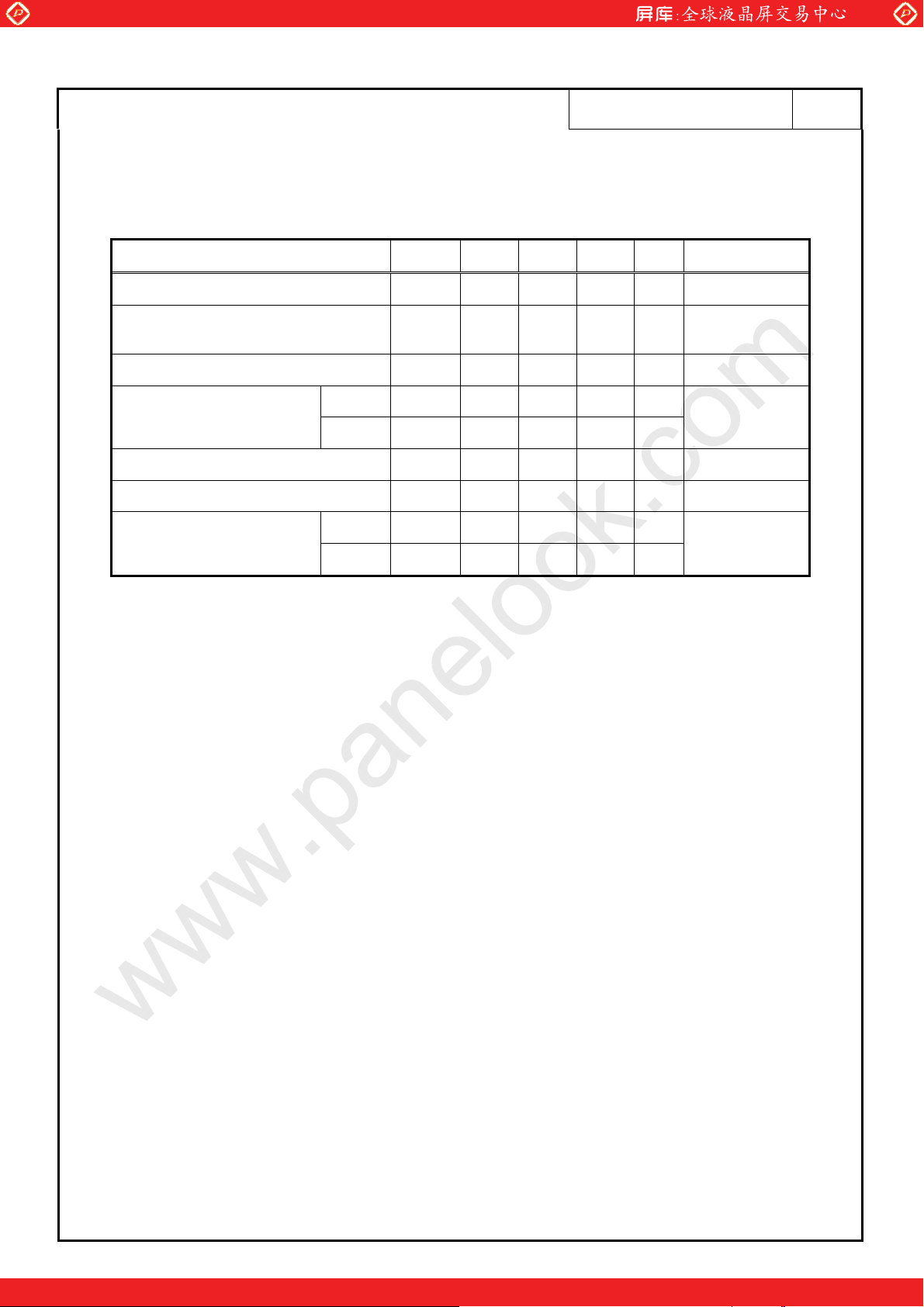
4.3 ELECTRICAL CHARACTERISTICS
4.3.1 Driving for LCD panel signal processing board
eter Symbol min. typ. max. Unit Remarks
Param
Power supply voltage VCC 3.0 3.3 3.6 V -
Power supply current ICC -
Permissible ripple voltage VRP - - 100 mV For VCC
Differential input threshold
voltage for LVDS receiver
Input vol
Terminating resister RT - 100 - -
Input voltage for MSL signal
tage width for LVDS receiver Vi 0 - 2.4 V -
Low VTL -100 - mV
High VTH - - +100 mV
Low VFL 0 - 0.8 V
High VFH 2.0 - VCC V
290
Note1
SN-SA-A0001-01-E 9/38
600
Note2
mA at VCC = 3.3V
at VCM = 1.2V
Note3
-
Note1: Checkered flag pattern (EIAJ ED-2522)
Note2: Pattern for maximum current
Note3: Common mode voltage for LVDS receiver
Shanghai SVA NEC Liquid Crystal Display Co., Ltd.
One step solution for LCD / PDP / OLED panel application: Datasheet, inventory and accessory!
www.panelook.com
Page 10
Global LCD Panel Exchange Center
www.panelook.com
SN-SA-A0001-01-E 10/38
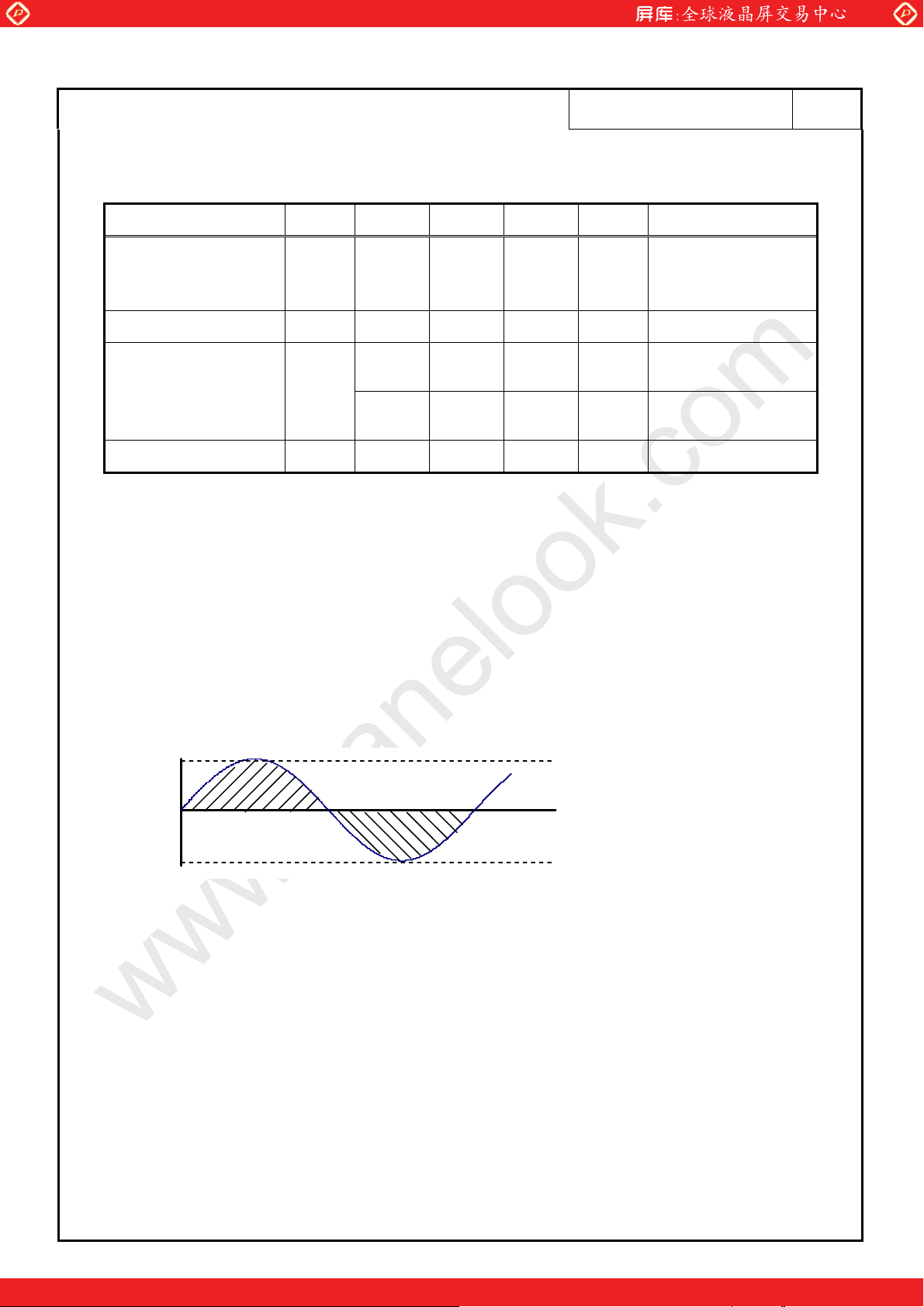
4.3.2 Driving for backlight lamp
Parameter Symbol min. typ. max. Unit Remarks
at IBL = 7.5mArms:
2
Lamp current IBL 3.5 7.5 8.0 mArms
Lamp voltage VBLH - 560 - Vrms Note2, Note3
1500 - - Vrms
Lamp starting voltage VS
1300 - - Vrms
tion FO 45 54 65 kHz Note4
Oscilla
L = 250cd/ m
Note3, Note5
Ta = 0ć
Note2, Note3
Ta = 25ć
Note2, Note3
(typ.)
Note1: This product consists of 2 backlight lamps, and these specifications are for each lamp.
Note2: The lamp voltage cycle between lamps should be kept on a same phase. “VS” and “VBLH”
are the voltage value between low voltage side (Cold) and high voltage (Hot).
Note3: The asymmetric ratio of working waveform for lamps (Lamp voltage peak ratio, Lamp
current peak ratio and waveform space ratio) should be less than 5% (See the following
figure). If the waveform is asymmetric, DC (Direct current) element applies into the lamp. In
this case, a lamp lifetime may be shortened, because a distribution of a lamp enclosure
substance inclines toward one side between low voltage terminal (Cold terminal) and high
voltage terminal (Hot terminal).
When design the backlight inverter, evaluate asymmetric of lamp working waveform
sufficiently.
Pa
Sa
Sb
Pb
Pa:
Supply voltage/current peak for positive, Pb: Supply voltage/current peak for negative
|Pa - Pb| / Pb × 100 5%
|Sa - Sb| / Sb × 100 5%
Sa: Waveform space for positive part, Sb: Waveform space for negative part
Note4: In case “FO” is not the recommended value, beat noise may display on the screen, because of
interference between “FO” and “1/th”. Recommended value of “FO” is as following.
FO = 1/4 x 1/th x (2n-1)
th: Horizontal signal period (See “4.9.2 Timing characteristics”.)
n: Natural number (1, 2, 3 ……)
Note5: Method of lamp cable installation may invite fluctuation of lamp current and voltage or
asymmetric of lamp working waveform. When design the backlight inverter, evaluate the
fluctuation of lamp current and voltage or asymmetric of lamp working waveform
sufficiently.
Shanghai SVA NEC Liquid Crystal Display Co., Ltd.
One step solution for LCD / PDP / OLED panel application: Datasheet, inventory and accessory!
www.panelook.com
Page 11
Global LCD Panel Exchange Center
www.panelook.com
SN-SA-A0001-01-E 11/38
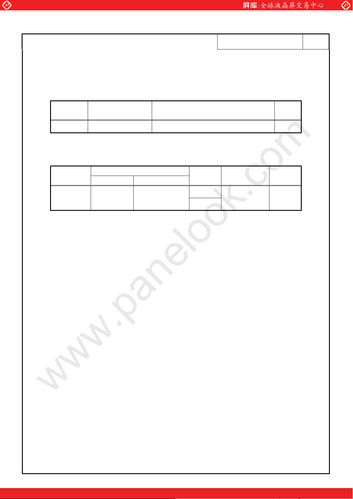
4.3.3 Power supply voltage ripple
This product works, even if the ripple voltage levels are beyond the permissible values as the
following table, but there might be noise on the display image.
Parameter Power supply voltage
VCC 3.3 V 10
(Measured at input terminal of power supply)
Ripple voltage Note1
0 mVp-p
Unit
Note1: The permissible ripple voltage includes spike noise.
4.3.4 Fuse
Parameter
Type Supplier
VCC TF16SN2.50 KOA Corporation
Fuse
Rating Fusing current Remarks
2.5 A
5.0 A Note1
32 V
Note1: The power supply capacity should be more than the fusing current. If the power supply
capacity is less than the fusing current, the fuse may not blow for a short time, and then nasty smell,
smoking and so on may occur.
Shanghai SVA NEC Liquid Crystal Display Co., Ltd.
One step solution for LCD / PDP / OLED panel application: Datasheet, inventory and accessory!
www.panelook.com
Page 12
Global LCD Panel Exchange Center
www.panelook.com
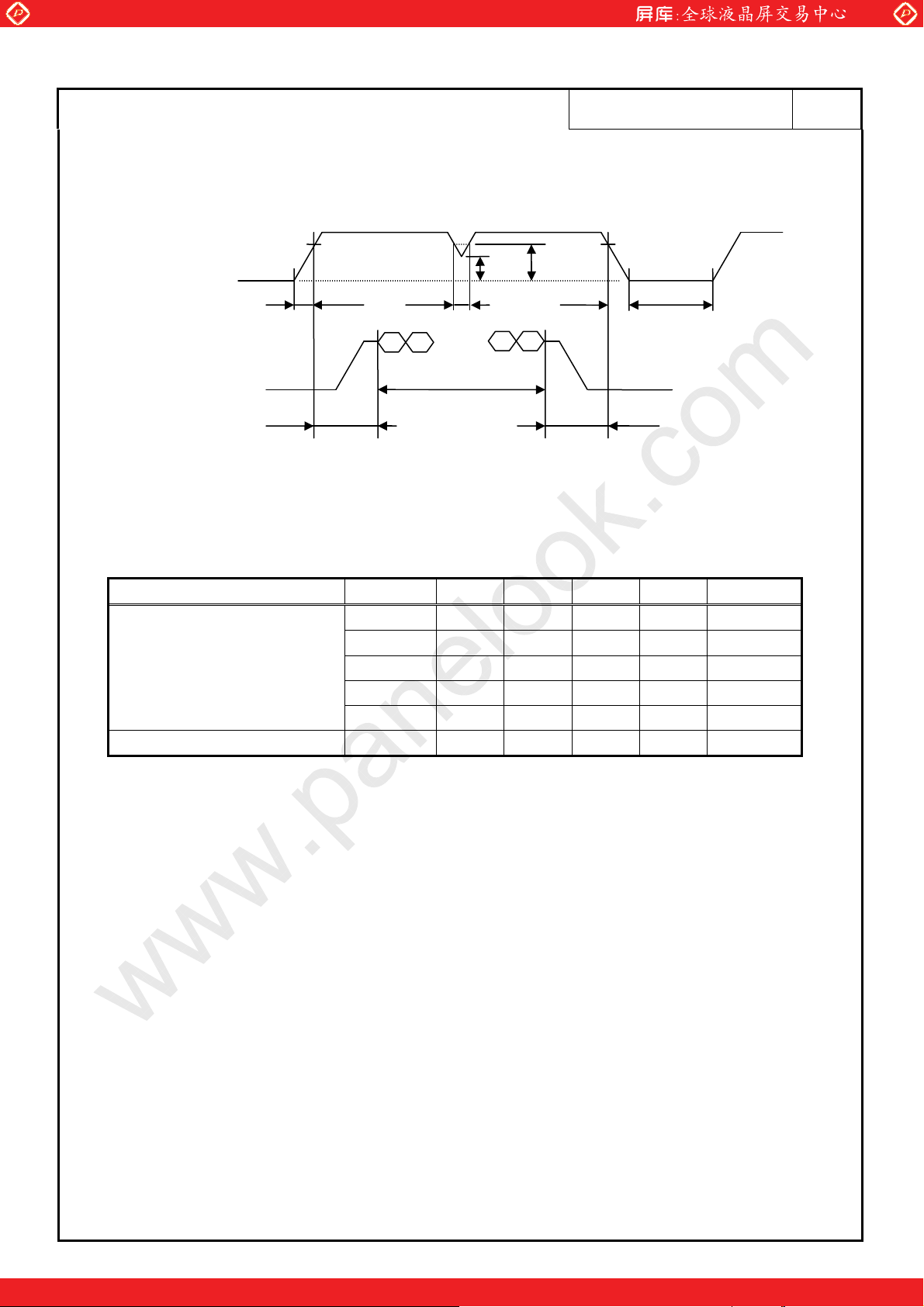
4.4 POWER SUPPLY VOLTAGE SEQUENCE
VCC ON VCC OFF
3.0 V
VCC
Note1
Display signals*
Function signal*
Note2
0 V
0 V
A
DE
FBC
VALID period
2.5 V
* These signals should be measured at the terminal of 100 resistor.
3.0 V
SN-SA-A0001-01-E 12/38
eter Symbol min. typ. max. Unit Remarks
Param
A--10ms-
B 0.0
Input voltage sequence
VCC DIP condition F - - 20 ms Note 3
C 500 - - ms -
D 0.01 - 50 ms -
E 0.01 - 50 ms -
1 - 10 ms -
Note1: In terms of voltage variation (voltage drop) while VCC rising edge is below 3.0 V, a
protection circuit may work, and then this product may not work.
Note2: Display signals (D0+/-, D1+/-, D2+/-, D3+/- and CK+/-) and function signal (MSL) must
be “0” voltage, exclude the VALID period (See above sequence diagram). If these signals
are higher than 0.3 V, the internal circuit is damaged.
If some of display and function signals of this product are cut while this product is
working, even if the signal input to it once again, it might not work normally. If customer
stops the display and function signals, they should be cut VCC.
Note3: VCC should be 2.5 V or more while VCC ON period.
Note4: The backlight power supply voltage should be inputted within the valid period of display
and function signals, in order to avoid unstable data display.
Shanghai SVA NEC Liquid Crystal Display Co., Ltd.
One step solution for LCD / PDP / OLED panel application: Datasheet, inventory and accessory!
www.panelook.com
Page 13
Global LCD Panel Exchange Center
www.panelook.com
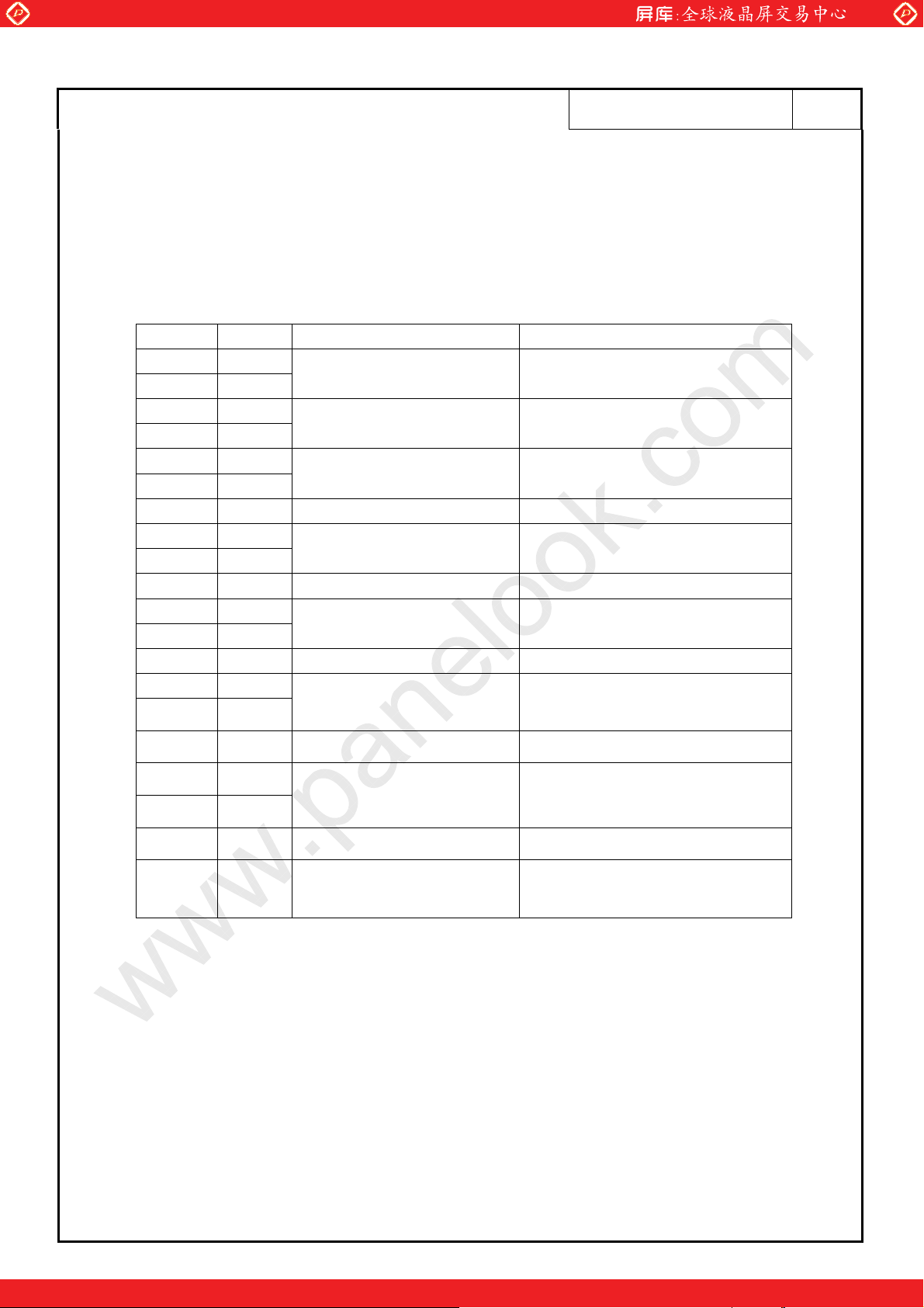
4.5 CONNECTIONS AND FUNCTIONS FOR INTERFACE PINS
4.5.1 LCD panel signal processing board
CN1 socket(Module side):DF-14H-20P-1.25H˄Hirose Electric Co., Ltd.˅
Adaptable plug˖ DF14-20S-1.25C˄Hirose Electric Co., Ltd.˅
Pin No. Symbol Signal Remarks
1 VCC
2 VCC
3 GND
4 GND
5 D06 D0+
7 GND Ground 8 D1-
9 D1+
10 GND Ground 11 D212 D2+
13 GND Ground 14 CLK-
15 CLK+
Power supply -
Ground -
Pixel data Note2
Pixel data Note2
Pixel data Note2
Pixel clock Note2
SN-SA-A0001-01-E 13/38
16 GND Ground -
17 D3-
Pixel data Note2
18 D3+
19 GND Ground -
20 MSL
Selection of LVDS input
Map Note1
High: Input map A mode
Low or Open: Input map B mode
Note1˖See“4.5.4 Connection between receiver and transmitter For LVDS” .
Note2˖Twist pair wires with 100(Characteristic impedance) should be connected between LCD
panel signal processing board and LVDS transmitter.
Shanghai SVA NEC Liquid Crystal Display Co., Ltd.
One step solution for LCD / PDP / OLED panel application: Datasheet, inventory and accessory!
www.panelook.com
Page 14
Global LCD Panel Exchange Center
N
www.panelook.com
SN-SA-A0001-01-E 14/38
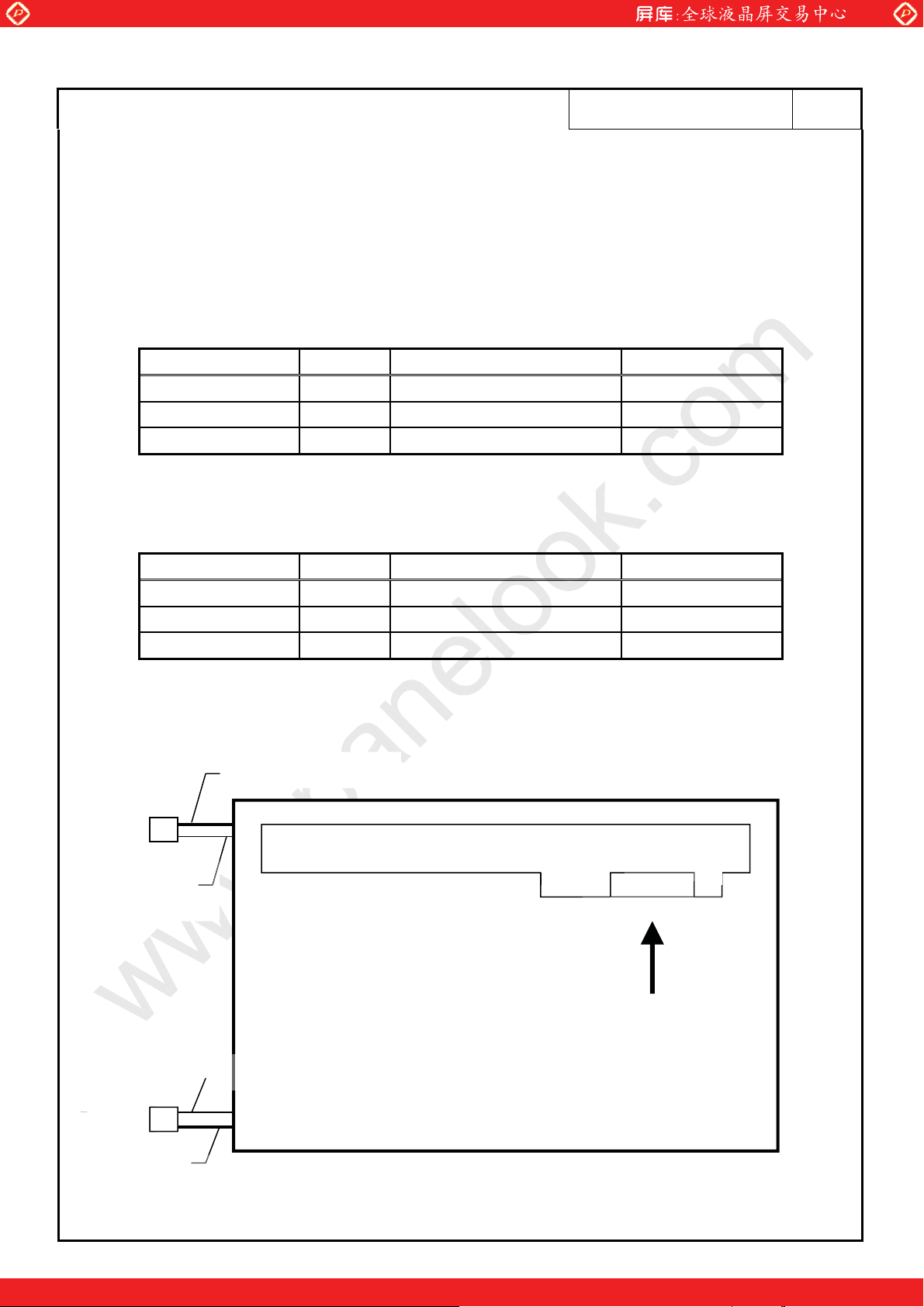
4.5.2 Backlight lamp
Attention: VBLH and VBLC must be connected correctly. IF customer connects wrongly,
customer will be hurt and the product will be broken.
CN201 plug˄LCD module side˅˖BHR-03VS-1˄J.S.T Mfg. Co., Ltd.˅
Adaptable socket˖ SM02˄8.0˅B-BHS-1-TB˄J.S.T Mfg. Co., Ltd.˅
Pin No. Symbol signal remarks
1 VBLH High voltage terminal(Hot) Cable color: Pink
2 N.C - -
3 VBLC Low voltage terminal(Cold) Cable color: White
CN202 plug˄LCD module side˅˖BHR-03VS-1˄J.S.T Mfg. Co., Ltd.˅
Adaptable socket˖ SM02˄8.0˅B-BHS-1-TB˄J.S.T Mfg. Co., Ltd.˅
Pin No. Symbol signal remarks
1 VBLH High voltage terminal(Hot) Cable color: Pink
2 N.C - -
3 VBLC Low voltage terminal(Cold) Cable color: White
4.5.3 Position of plugs and a socket
High voltage (Hot)
1
CN201
3
3
Low voltage
(Cold)
Signal processing board
CN1
2
0 1
Insert direction
Low volatge(Cold)
3
CN202
C
202
1
High voltage (Hot)
Shanghai SVA NEC Liquid Crystal Display Co., Ltd.
One step solution for LCD / PDP / OLED panel application: Datasheet, inventory and accessory!
www.panelook.com
Page 15
Global LCD Panel Exchange Center
VCC
www.panelook.com
SN-SA-A0001-01-E 15/38
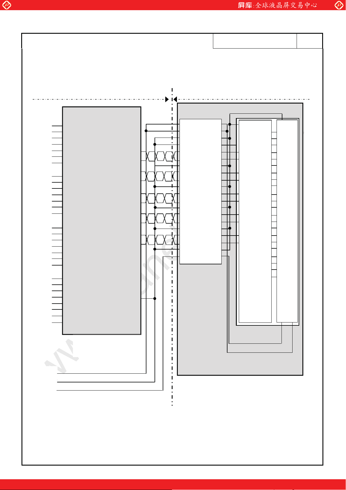
4.5.4 Connection between receiver and transmitter for LVDS
(1) Input LVDS map A (MSL :”High”)
Host LCD Module(Product)
R2
R3
R4
R5
R6
R7
G2
G3
G4
G5
G6
G7
B2
B3
B4
B5
B6
B7
High or Low
High or Low
DE
R0
R1
G0
G1
B0
B1
RSVD
CLK
TA0
TA1
TA2
TA3
TA4
TA5
TA6
TB0
TB1
TB2
TB3
TB4
TB5
TB6
TC0
TC1
TC2
TC3
TC4
TC5
TC6
TD0
TD1
TD2
TD3
TD4
TD5
TD6
CLK IN
Transmitter for LVDS
Note1
TA-
TA+
TB-
TB+
TC-
TC+
TCLK-
TCLK+
TD-
TD+
GND
1 VCC
2 VCC
3 GND
4 GND
5 D06 D0+
7 GND
8 D19 D1+
10 GND
11 D212 D2+
13 GND
14 CLK15 CLK+
16 GND
17 D318 D3+
19 GND
20 MSL
CN1 Socket
GND
RARA+
RB+
RB-
RC+
RC-
RCLKRCLK+
RDRD+
Receiver for
LVDS
Equivalent of
THC63LVDF84A
LCD controller
GND
Signal
processor
MSL
VCC
VCC
GND
“
High”
LCD panel processing board
Note1: Recommended transmitter
See the data sheet for THC
Not
e2: LSB˄Least Significant Bit˅-R0,G0,B0 MSB˄Most Significant Bit˅-R7,G7,B7
One step solution for LCD / PDP / OLED panel application: Datasheet, inventory and accessory!
63LVDF3A and THC63LVDM83R˄THine Electronics Inc.˅.
Shanghai SVA NEC Liquid Crystal Display Co., Ltd.
www.panelook.com
Page 16
Global LCD Panel Exchange Center
www.panelook.com
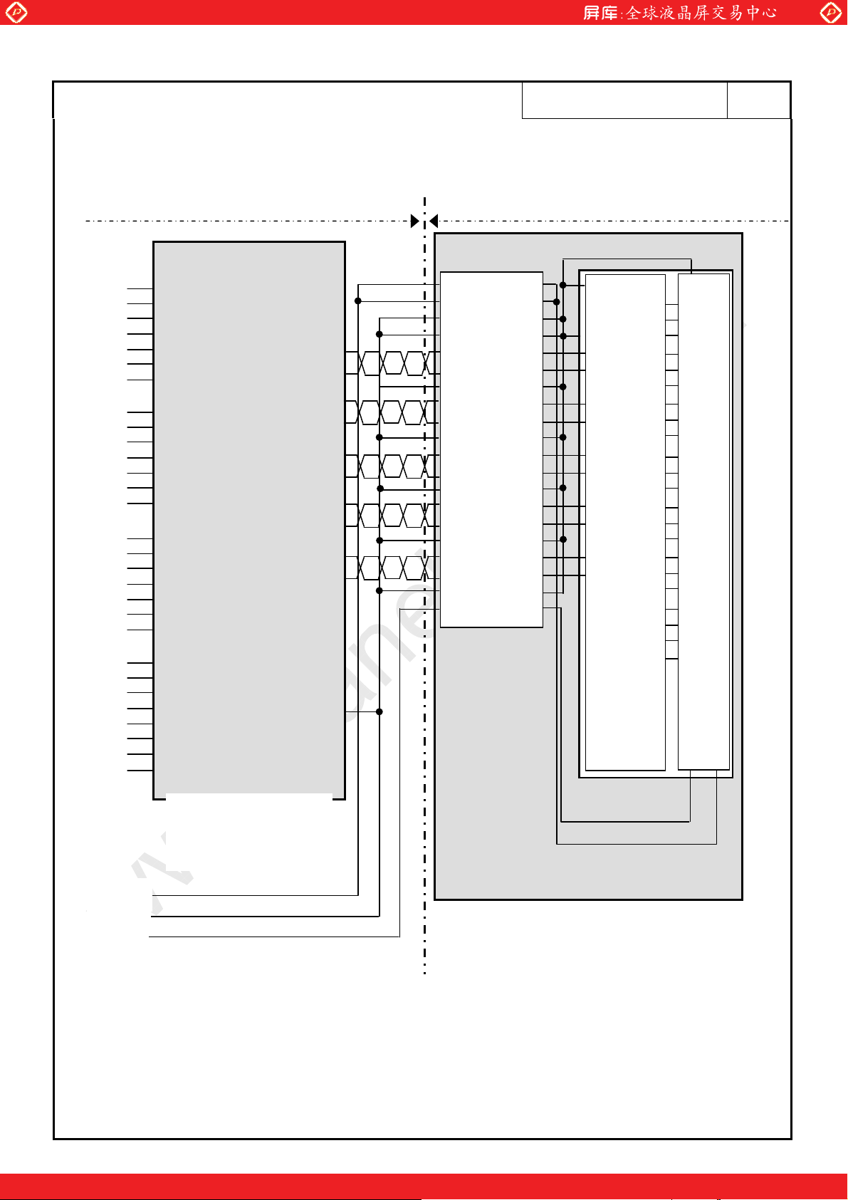
(2) Input LVDS map B(MSL :”Low”or”Open”)
Host
R0
R1
R2
R3
R4
R5
G0
G1
G2
G3
G4
G5
B0
B1
B2
B3
B4
B5
igh or L
H
High or Low
RS
ow
DE
R6
R7
G6
G7
B6
B7
VD
CLK
TXIN0
TXIN1
TXIN2
TXIN3
TXIN4
TXIN6
TXIN7
XIN8T
TXIN9
TXIN12
TXIN13
TXIN14
TXIN15
TXIN18
XIN19T
TXIN20
TXIN21
TXIN22
TXIN24
TXIN25
TXIN26
XIN27T
TXIN5
TXIN10
TXIN11
TXIN16
TXIN18
TXIN23
CLK IN
TX
TXOUTCLK+
Transmitter for LVDS
DS90C383
Note1
TXOUT
TXOUT+
XOUT1-
T
TXOUT1+
OUT2TX
TXOUT2+
OUTCLK-
TXOUT3-
TXOUT3+
GND
-
-
SN-SA-A0001-01-E 16/38
LCD Module(Product)
1 VCC
2 VCC
3 GND
4 GND
5 D06 D0+
7 GND
8 D19 D1+
10 GND
11 D212 D2+
13 GND
14 CLK15 CLK+
16 GND
17 D318 D3+
19 GND
20 MSL
CN1 Soc
ket
GND
R
A-
RA+
R
B+
RB-
C+R
RC-
CLR
K-
RCLK+
D-R
RD+
Receiver for
LVDS
Equivalent of
T
HC63LVDF84A
LCD controller
GND
Signal
processor
MSL
VCC
VCC
GND
LCD panel processing board
“High”
Note1: Recommended transmitter
See the data sheet for DS90C383˄National Semiconductor˅.
Note2: LSB˄Least Significant Bit˅
One step solution for LCD / PDP / OLED panel application: Datasheet, inventory and accessory!
-R0,G0,B0 MSB˄Most Significant Bit˅-R7,G7,B7
Shanghai SVA NEC Liquid Crystal Display Co., Ltd.
www.panelook.com
Page 17
Global LCD Panel Exchange Center
www.panelook.com
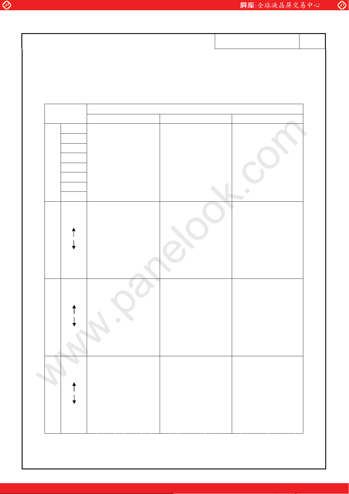
4.6 DISPLAY COLORS AND INPUT DATA SIGNALS
This product can display in equivalent to 16,777,216
display colors and input data signals is as the following table.
Display colors
Black 0 0 0 0 0 0 0 0 0 0 0 0 000000000000
Blue 0 00 0 0 0 000000000011 1 1 1 1 11
Red 1 11 1 1 1 110000000000 0 0 0 0 00
Magenta 1 1 1 1 1 1 1 1 0 0 0 0 0 0 0 0 1 1 1 1 1 1 1 1
Green 0 0 0 0 0 0 0 0 1 1 1 1 1 1 1 1 0 0 0 0 0 0 0 0
Basic Color
Cyan 0 00 0 0 0 001111111111 1 1 1 1 11
Yellow 1 1 1 1 1 1 111111111100 0 0 0 0 00
White 1 1 1 1 1 1 111111111111 1 1 1 1 11
Black
Dark
Bright
Red grayscale
Red
Black
Dark
Bright
Green grayscale
Green
Black
Dark
Bright
Blue grayscale
Blue
R7 R6 R5 R4 R3 R2 R1 R0 G7 G6 G5 G4 G3 G2 G1 G0 B7 B6 B5 B4 B3 B2 B1 B0
0 00 0 0 0 000000000000 0 0 0 0 00
0 00 0 0 0 010000000000 0 0 0 0 00
0 00 0 0 0 100000000000 0 0 0 0 00
: : :
: : :
1 11 1 1 1 010000000000 0 0 0 0 00
1 11 1 1 1 100000000000 0 0 0 0 00
1 11 1 1 1 110000000000 0 0 0 0 00
0 00 0 0 0 000000000000 0 0 0 0 00
0 00 0 0 0 000000000100 0 0 0 0 00
0 00 0 0 0 000000001000 0 0 0 0 00
: : :
: : :
00 0 0 0 001111110100 0 0 0 0 00
0
0 00 0 0 0 001111111000 0 0 0 0 00
0 00 0 0 0 001111111100 0 0 0 0 00
0 00 0 0 0 000000000000 0 0 0 0 00
0 00 0 0 0 000000000000 0 0 0 0 01
0 00 0 0 0 000000000000 0 0 0 0 10
: : :
: : :
0 00 0 0 0 000000000011 1 1 1 1 01
0 00 0 0 0 000000000011 1 1 1 1 10
0 00 0 0 0 000000000011 1 1 1 1 11
Data sign
al ˄0:Low levelˈ1:
colors in 256 scale. Also the relation between
High Lev
SN-SA-A0001-01-E 17/38
el˅
Shanghai SVA NEC Liquid Crystal Display Co., Ltd.
One step solution for LCD / PDP / OLED panel application: Datasheet, inventory and accessory!
www.panelook.com
Page 18
Global LCD Panel Exchange Center
www.panelook.com
SN-SA-A0001-01-E 18/38
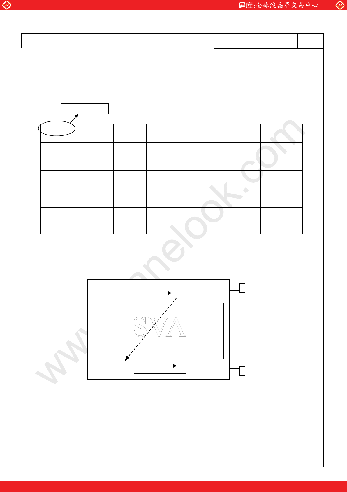
4.7 DISPLAY POSITIONS
The following table i
s the coordinates per pixel(See ”4.8 SCANNING DIRECTIONS”.).
C˄1ˈ1˅
R G B
C˄1ˈ C2 ˅ ••• C˄Xˈ1˅ ••• C˄1023ˈ1˅ C˄1024ˈ1˅1˅˄ˈ1
C˄1ˈ2˅ C˄2ˈ2˅ ••
•
•
•
C˄1ˈ˅ C˄2ˈ˅ C˄XY˅ C˄10 ˈY˅ C˄10 ˈY˅Y Y ••• ˈ ••• 23 24
•
•
•
•
•
•
•
•
•
• C˄XˈY˅ ••• C˄1023ˈ2˅ C˄1024ˈ2˅
•••
••
•
•
•
•
•
•
•
•
•
•
•
•
•••
•
•
•••
•
•
•
•
•
•
•
•
•
•
•
•
•
C˄1ˈ 7˅ C˄2ˈ 7˅ C˄X7˅ C˄102 767˅ C˄102 767˅76 76 ••• ˈ76 ••• 3ˈ 4ˈ
C˄176
8 SCANNING DIRECTIO
4. NS
The following figures are seen fro
8 Cˈ˅ ˈ˅ ˈ˅ ˈ˅ ˈ˅˄2768 ••• C˄X 768 ••• C˄1023 767 C˄1024 768
m a front view. Also the arrow shows the direction of scan.
C(1,1)
D(1,1)
C(1,768)
D(1,768)
C(1024,1)
D(1024,1)
C(1024,768)
D(1024,768)
Note1: Meaning of C(X,Y) and D(X,Y)
C(X,Y): The coordinates of the display osition(See”4.7 DISPLAY POSITIONS”.)
D(X,Y): The data number of input si
One step solution for LCD / PDP / OLED panel application: Datasheet, inventory and accessory!
p
gnal for LCD panel signal processing board.
Shanghai SVA NEC Liquid Crystal Display Co., Ltd.
www.panelook.com
Page 19
Global LCD Panel Exchange Center
www.panelook.com
SN-SA-A0001-01-E 19/38
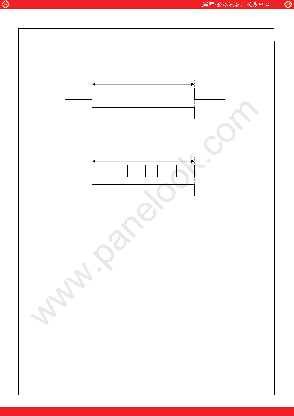
4.9 INPUT SIGNAL TIMINGS FOR LCD PANEL SIGNAL PROCESSING BOARD
4.9.1 Outline of input signal timings
gHorizontal signal
Horizontal display period (thd)
DE (Data enable)
Display period
Note1
te
No 1: This diagram indicates virtual signal for set up to timing.
gV
ertical signal
Vertical display period (tvd)
DE (Data enable)
1 2 3 4 768
Display period
Note1
No
te1: This diagram indicates virtual signal for set up to timing.
Shanghai SVA NEC Liquid Crystal Display Co., Ltd.
One step solution for LCD / PDP / OLED panel application: Datasheet, inventory and accessory!
www.panelook.com
Page 20
Global LCD Panel Exchange Center
www.panelook.com
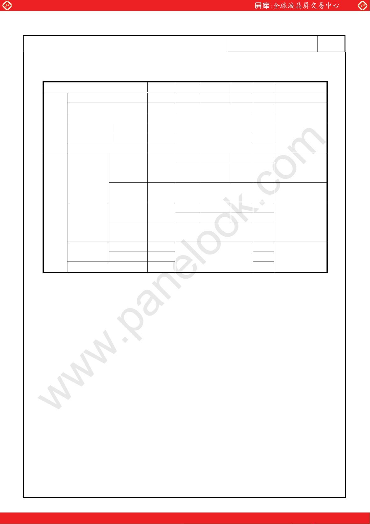
4.9.2 Timing characteristics
(Note1)
Frequency 1/tc 60.0 65.0 70.0 MHz 15.384ns˄typ.˅
CLK
DATA
DE
Rise me time, Fall ti ˉ
CLeK-DATA
Rise time, ll time ˉ ns
Ho
V
ertical
(One frame)
CLK-DE
Rise tim all time
rizontal
Du
ty ˉ
Fa
e, F
Symbol min. typ. max. Unit Remarks Parameter
ˉ
Setup time ˉ ns
Hold tim ˉ ns
12.3 2 6 ˉ μs 0.67
Cycle th
D
isplay
period
Cycle tv
D
isplay
period
Setup time ˉ ns
Hold time
t
hd 1024 ˉ
tvd 768 H
ˉ ns
1050 1344 18 CLK
13.1 20.0 m16.666 s
770 80 ˉ H 6
ˉ
ˉ
ˉ
SN-SA-A0001-01-E 20/38
ns
00
Note2
Note2
48.36 yp.)
3KHz(t
Note3
Note4
60.0Hz˄typ.˅
Note2
ns
Note1˖ rameters is follows.
Definition of pa
tc=1CLK,Th=1H
Note 2˖See the data sheet of LVDS transmitter
Note 3˖Both of “time” and “
CLK number” of the “th” must keep the Minimum value of
.
specifications.
Note 4˖“th” must keep the fluctuation within ±1 CLK, because of avoidance of image
sticking.
Shanghai SVA NEC Liquid Crystal Display Co., Ltd.
One step solution for LCD / PDP / OLED panel application: Datasheet, inventory and accessory!
www.panelook.com
Page 21
Global LCD Panel Exchange Center
www.panelook.com
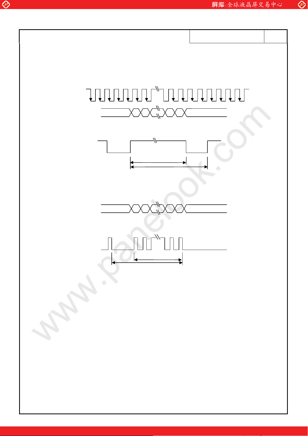
4.9.3 Input signal timing chart
Horizontal timing
CLK
DATA
(R0-R7)
(G0-G7)
(B0-B7)
DE
Invalid 1 2 1023 1024 Invalid
SN-SA-A0001-01-E 21/38
thd
th
Vertical timing
DATA
(R0-R7)
(G0-G7)
(B0-B7)
DE
Invalid 1 2 767 768 Invalid
tvd
tv
Shanghai SVA NEC Liquid Crystal Display Co., Ltd.
One step solution for LCD / PDP / OLED panel application: Datasheet, inventory and accessory!
www.panelook.com
Page 22
Global LCD Panel Exchange Center
www.panelook.com
SN-SA-A0001-01-E 22/38
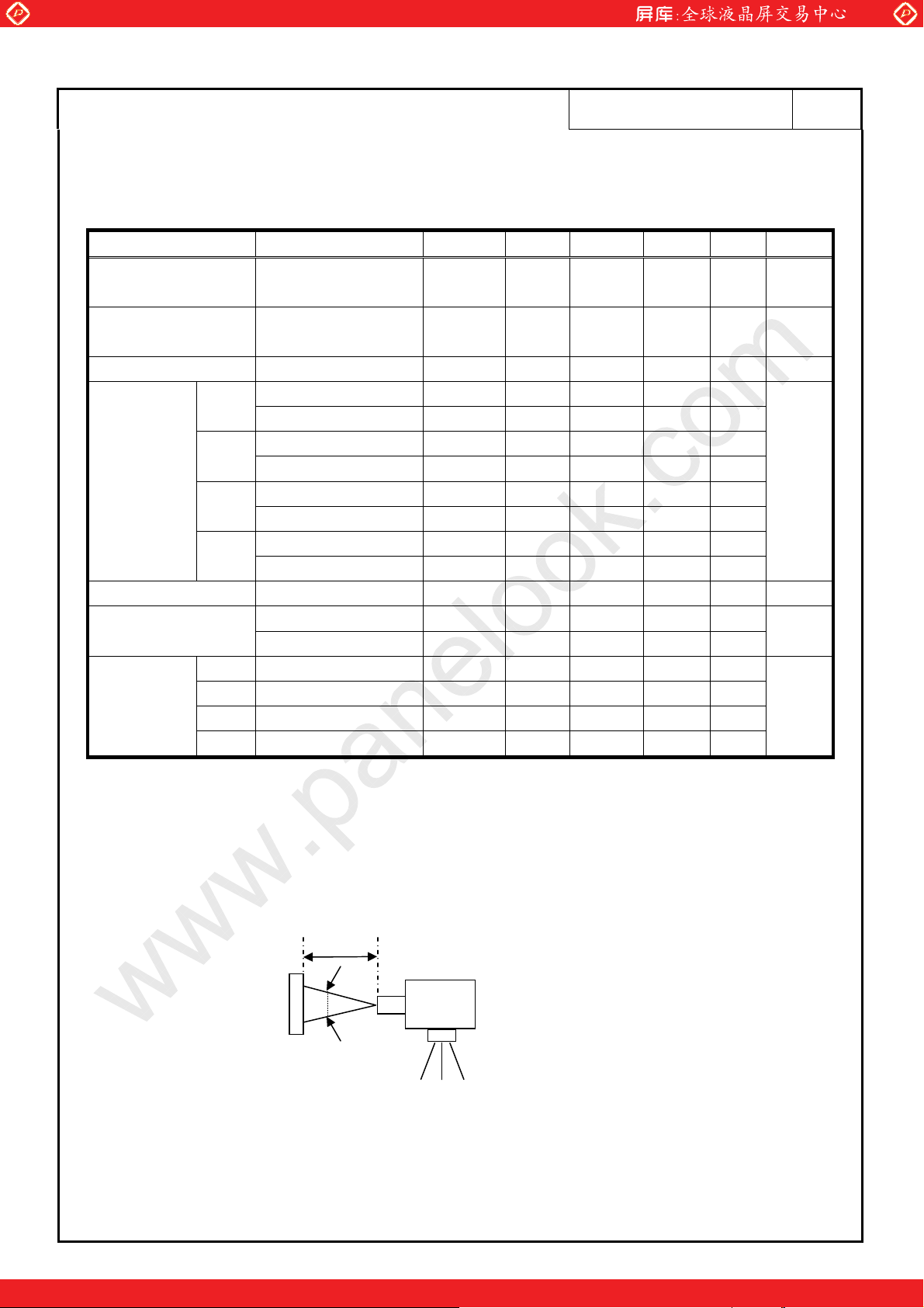
4.10 OPTICS
4.10.1 Optical characteristics
ition Symbol min. typ. max. Unit RemarksParameter Note1 Cond
Luminance
Contrast r
Luminance uniformity LU - 1.1 1.3 - Note 3-
White
Red
Chromaticity Note 4
Green
Blue
Color gamut R=0, 50 %L=0, U=0,D=0 C 60 -
Response time
Right U=0°, 60D=0°,CR=10 R 50 -
Viewing angle
Left U=0°, D=0°,CR=10 L 50 60 -
Up R=0°, L=0°,CR=10 U 30 40 -
Down
White at
R=0, L=0 D=0
Wh
ite/Black at center
R=0
ˈ L=0, U=0,D=0
White to T 15 ms black on - 8
Black to white of - 17
R=0°, L=0°,CR=10 D 35 60 -
center
, U=0,
X coordinate Wx 0.283 0.313 0.343 -
Y 0.299 0.329 0.359 coordinate Wy -
X coordinate Rx - 0.624 - -
Y coordinate Ry - 0.351
X coordinate Gx - 0.325 - -
X coordinate Bx - 0.144 - -
Y coordinate By - 0.100 - -
L 200 250 - cd/ m
CR 300 Note2atio
T f 25 ms
400 - -
-Y coordinate Gy - 0.571 -
DŽ
DŽ
DŽ
DŽ
2
-
Note 4
Note 5
Note 6
Note1˖ easu are fo s.
M rement conditions llow
5C BL=7. Arms/lampˈDisplay mo ˖XGAˈHorizontal
Ta=2 ˈVCC=3.3VˈI5m de
cycle=48.363 KHzˈVertical cycle=60.0
00Hz
ptical characteristics are measured aO t luminance saturation after 20minutes from
w
orking the product, in the dark room. Also measurement method for luminance is as
fo
llows.
50cm
Photodetector (TOPCON BM-5A)
LCD module 1嘙
(Product)
ote 2˖See
N “4.10.2 Definition of contrast ratio”.
Note 3˖See
Note 4 Product surface temperature˖TopF=28.0
˖
“4.10.3 Definition of luminance uniformity”.
ć
Note 5˖See “4.10.4 Definition of response times”.
Note 6˖See “4.10.5 Definition of viewing angles”.
Shanghai SVA NEC Liquid Crystal Display Co., Ltd.
One step solution for LCD / PDP / OLED panel application: Datasheet, inventory and accessory!
www.panelook.com
Page 23
Global LCD Panel Exchange Center
ķ
ĸ
Ĺ
ĺ
Ļ
www.panelook.com
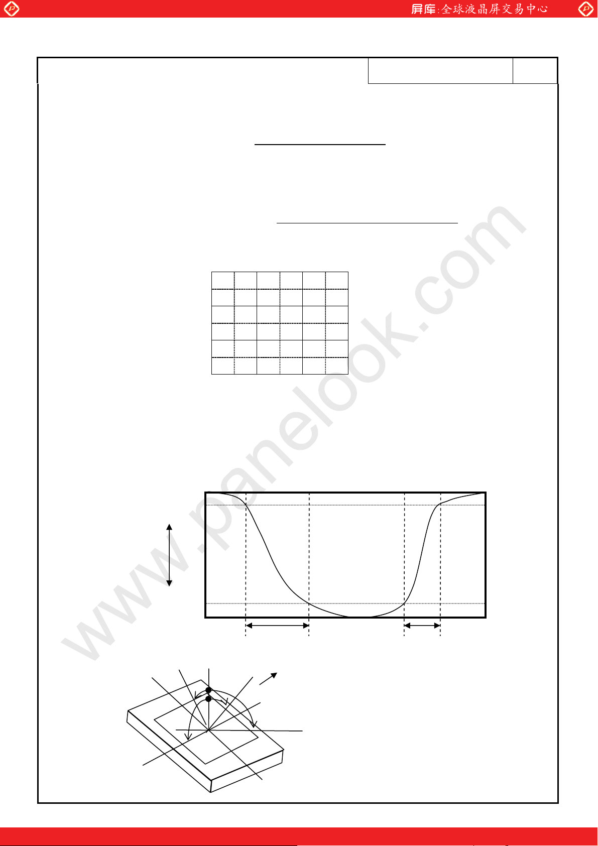
4.10.2 of contrast ratio
The contrast ratio is calculated by using the following formula.
Contrast ratio˄CR
Luminance of black screen
4.10.3 Definition of luminance uniformity
The luminance uniformity is calculated by using the following formula.
Minimum luminance from ķWR
The
Definition
˅= Luminance of white screen
Luminance uniformity˄LU˅=
Maximum luminance from ķWRĻ
luminance is measured at near the 5 points shown below.
171 512 853
126
384
640
ķ
SN-SA-A0001-01-E 23/38
Ļ
4.10.4 Definition of response times
Response time is measured, the luminance changes from “white” to “black”, or “black” to
“white” on the same screen
ange from 90% down to 10%. Also Toff is the time it takes the luminance change from
ch
10% up to 90%. (See the following diagram.)
0%
10
90%
White
Luminance
Bla
4.10.5 Definition of
Left
ck
10%
0%
Ton Toff
viewing angles
Normal axis (Perpendicular)
©/
©8
©'
point, by photo-detector. Ton is the time it takes the luminance
12 o’clock
Up
per
©5
Right
Lower
Shanghai SVA NEC Liquid Crystal Display Co., Ltd.
One step solution for LCD / PDP / OLED panel application: Datasheet, inventory and accessory!
www.panelook.com
Page 24
Global LCD Panel Exchange Center
www.panelook.com
SN-SA-A0001-01-E 24/38
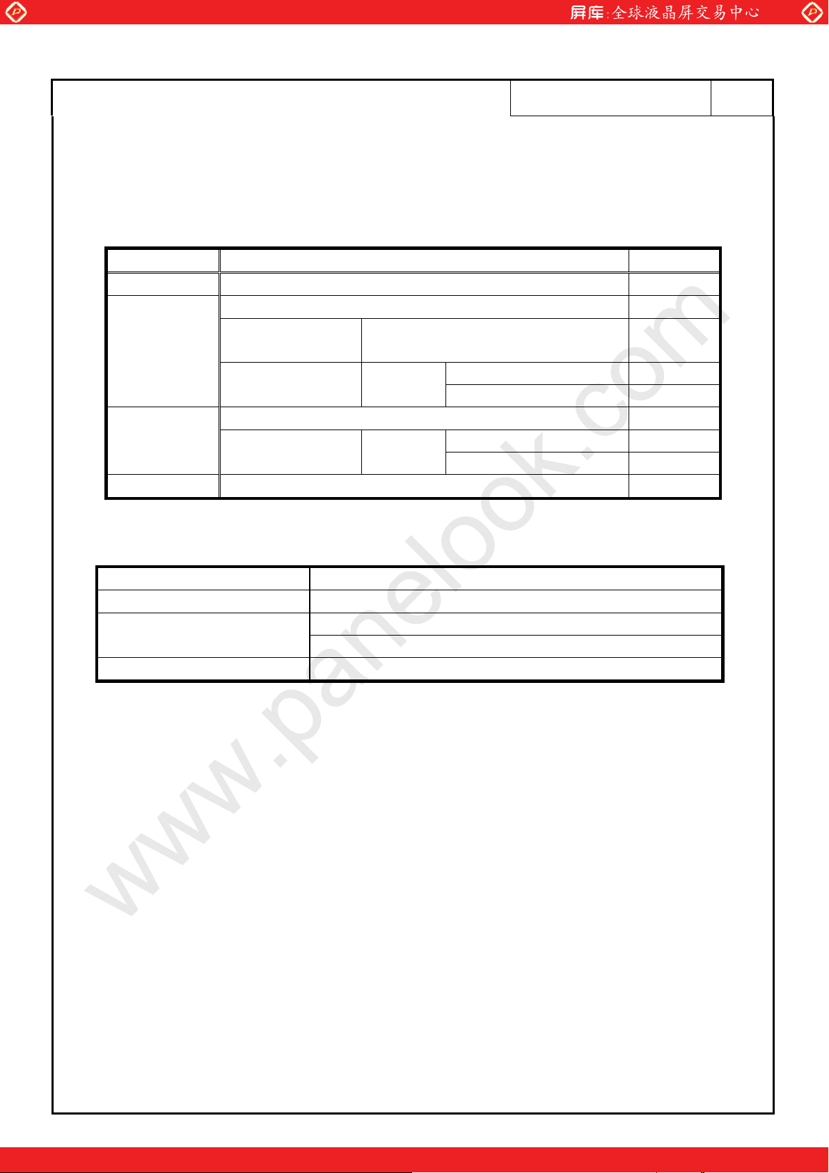
4.11 DEFECT CRITERIA
4.11.1 Display specifica
tion
(Note1, Note 2)
Defect pattern
Condition Criteria
Line defect Display of black, white, red, green, blue 0 line
4 dots
1 set
0 set
0 set
Bright dots
Note 2
Note 3
Dark dots
Note 2
Note 4
R+G+B
Close de
fect dots
Note 6 Note 5
L
inked defect dots
Note 7
D=0mm
Note 5
R+G+B 4 dots
Linked defect dots
Note 7
D
=0mm
N
ote 5
˘D6.5mm
0mm
2 defect dots 2 sets
3 defect dots or more
2 defect dots 2 sets
3 defect dots or more
Total Brig ark dotsht dotsˇD 8 dots
Note spection conditions are
1˖In as follows.
Temperature
25±5
ć
Inspection viewing distance 20cm(The distance between the inspector’s eye and screen)
L
Inspection direction
0°R2
0°
R20°
20°0°ˈ0°
Inspection illumination 60lx(at a display surface)
N of one dot
ote 2˖Defect area > 1/2
Dot defects are include intermittent bright and dark dot.
Dots darker than half brightn
and dots brighter than half brightness of full bright do
ess of full bright dots are not defined as bright dot defect,
ts are not defined as dark dot
defect.
Note 3˖
Note 4˖ ts are counted while the display is illuminated with Red, Green or Blue.
Bright dots are counted while the display is black.
Dark do
Note 5˖D is the distance between defect dots.
Note 6˖See“4.11.2
Note 7˖See“4.11.3
Close defect dots”.
Linked defect dots”.
Shanghai SVA NEC Liquid Crystal Display Co., Ltd.
One step solution for LCD / PDP / OLED panel application: Datasheet, inventory and accessory!
www.panelook.com
Page 25
Global LCD Panel Exchange Center
www.panelook.com
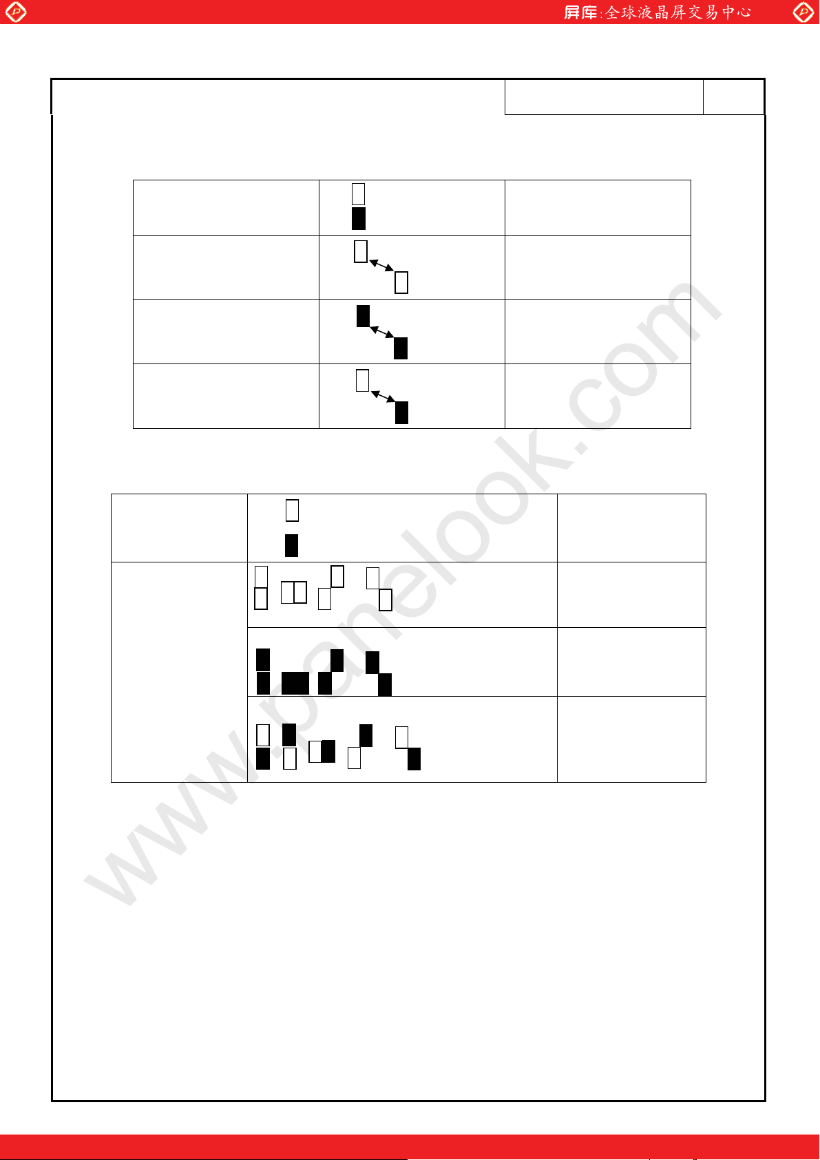
4.11.2 Close defect dots
Defect pattern
Bright dots
Dark dots Allowed
Combinati en bright
4.11.3 Linked
ons betwe
dot and dark dot
defect dots
: Bright dot
: Dark dot
0mm˘D
SN-SA-A0001-01-E 25/38
Criteria
6.5mm
1 set
Allowed
: Bright dot
Defect pat
ˎdefec
tern
t dots
: Dark dot
Combination between bright dotsand dark dot
Etc.
Criteria
2 sets
2 sets
Allowed
Shanghai SVA NEC Liquid Crystal Display Co., Ltd.
One step solution for LCD / PDP / OLED panel application: Datasheet, inventory and accessory!
www.panelook.com
Page 26
Global LCD Panel Exchange Center
www.panelook.com
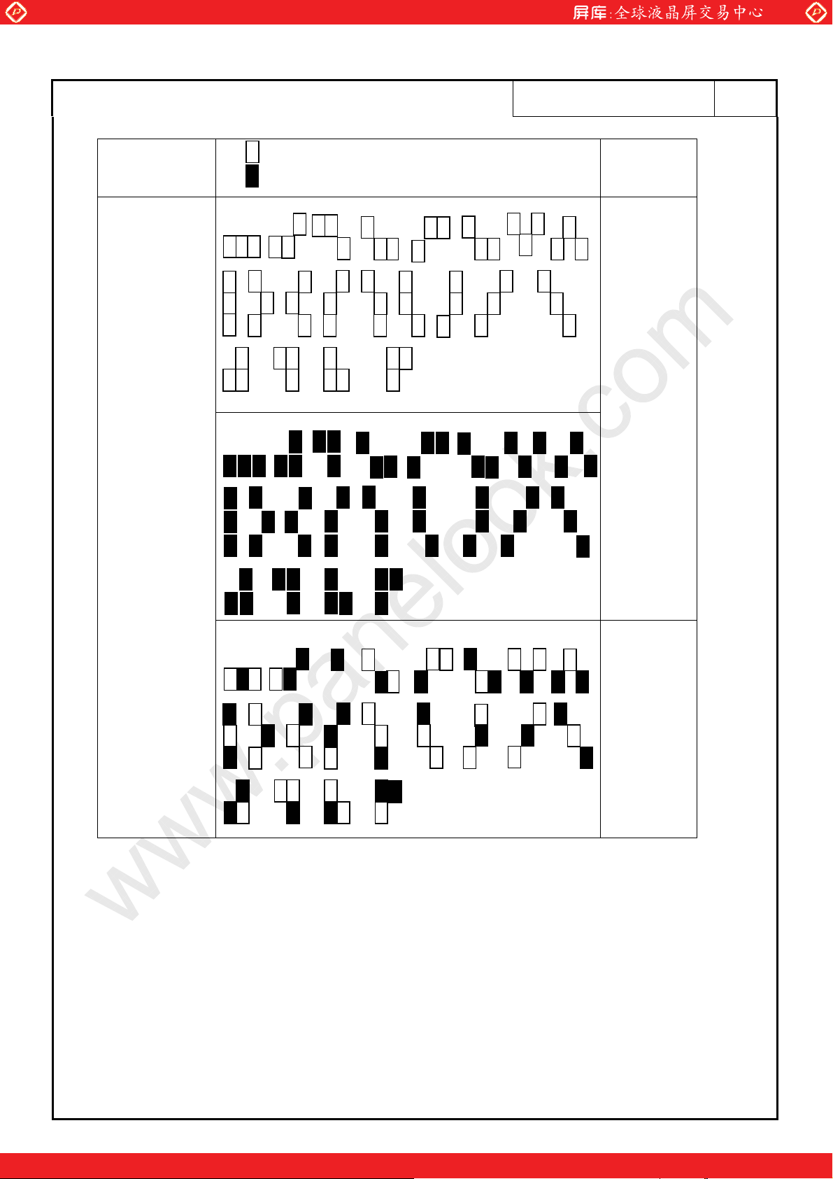
Defect pattern
: Bright dot
: Dark dot
SN-SA-A0001-01-E 26/38
Criteria
Bright dot
0 set
Dark dot
3 defect dots
Combinations between bright dot and dark dot
Etc.
Allowed
Shanghai SVA NEC Liquid Crystal Display Co., Ltd.
One step solution for LCD / PDP / OLED panel application: Datasheet, inventory and accessory!
www.panelook.com
Page 27
Global LCD Panel Exchange Center
www.panelook.com
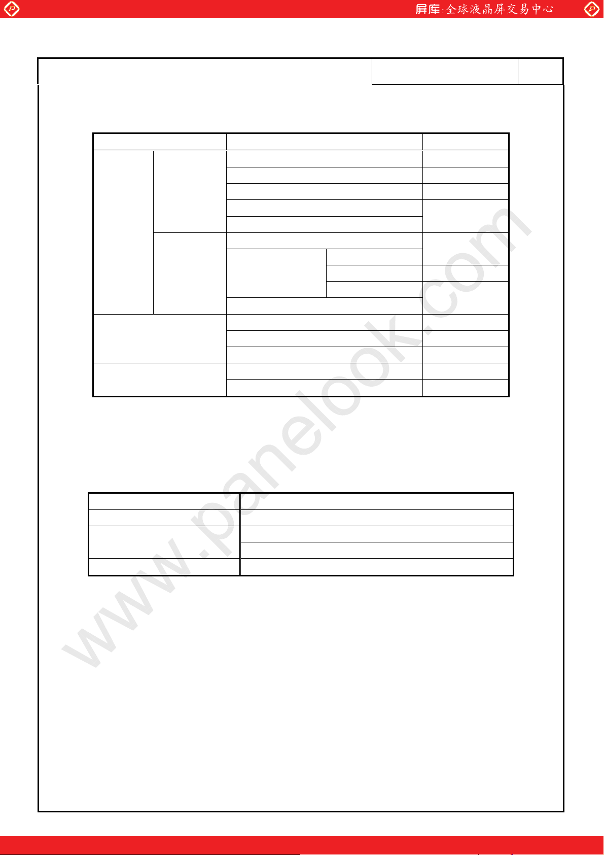
4.11.4 Appearance specifications
Dot shape
Im
pure
ingredient
Stains
Dust
Line shape
ubbles, Wrinkies, Dent
B
Polarizer scratch
Condition Note l Criteria Defect pattern
d<0
0.2m İmİd<0.3mm 10 points
0.3mm mm İİdİ0.5 3 points
d>0.5mm
Adjacent other objects
W<0.05mm
0.05mmİWİ0.1mm
W>0 m
dİ0.2mm
0.2m m İm<dİ0.5m 2 points
d>0.5mm 0 point
S0.2mm
S>0.2mm
SN-SA-A0001-01-E 27/38
.2mm Allowed
0 point
L<0.7mm
0.7mmİLİ1.0mm
L>1.0mm
.1m
2
2
Allowed
İ4 points
0 point
Allowed
Allowed
0 point
Note1: Defin is as follows.
ition of symbols
d: Average diameter
(This diameter is the average length
W: Width, L: Length,
Note2: I
nspection conditions are as follows.
Temperature
Inspec
tion viewing distance 20cm (The distance between the inspector’s eye and screen.)
tion direction
Inspec
ination 700lx face)(at an inspection desk sur
Illum
S: Area
of a long axis and a short axis in each defect pattern.)
25±5ć
0°R L45°45°, 0°
0°U45°, 0°D45°
Shanghai SVA NEC Liquid Crystal Display Co., Ltd.
One step solution for LCD / PDP / OLED panel application: Datasheet, inventory and accessory!
www.panelook.com
Page 28
Global LCD Panel Exchange Center
www.panelook.com
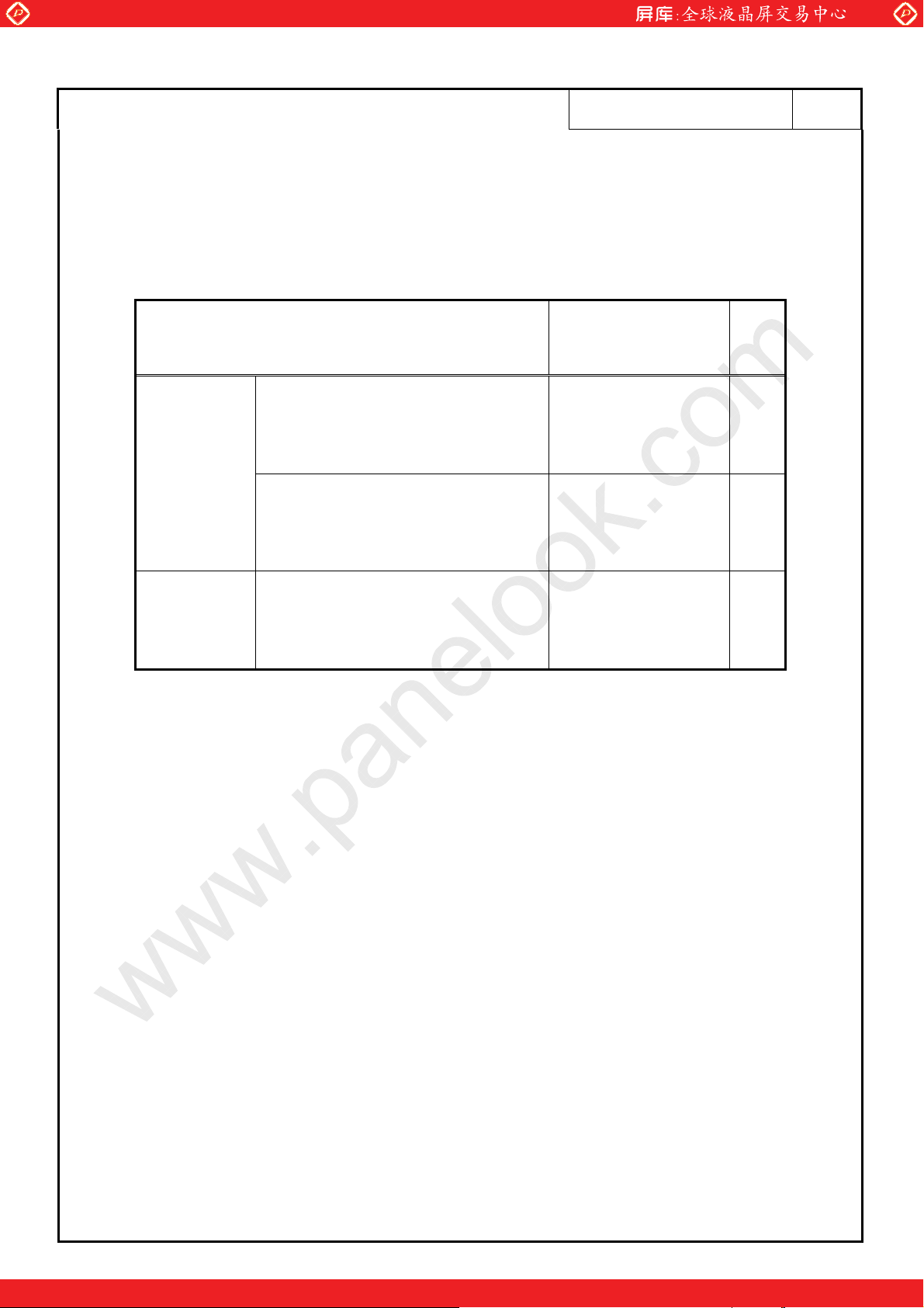
5. ESTIMATED LUMINANCE LIFETIME
The luminance lifetime is the time from initi
This lifetime is the estimated value, and is not guarantee value.
dition
Con
25 t temperature of the
(Ambienć
product)
Continuous operation and
IBL=7 p
Module
Cold cathode
Fluorescent
lamp
(Surface temperature at scr
50 eenć
Continuous operation and
25 heć
(Ambient temperature of t
Continuous operation and
.5mArms/lam
center)
IBL=7. /lamp
IBL=7 p
5mArms
product)
.5mArms/lam
al luminance to half-luminance.
SN-SA-A0001-01-E 28/38
Luminance
lifetime(MTTF) Unit
Note1,Note2
40,000 h
35,000 h
50,000 h
Note1: MTTF is m e to half-
ote2: In case the product works under low temperature environment, the lifetime becomes short.
N
ean tim luminance.
6. PRODUCT INSPECTIONS
The following inspections are c
arried out for products, before shipment
(1) 100% inspection:
噝Power supply current
噝Display
噝Appearance
(2) S ction:
ampling inspe
噝White luminance
噝Contrast
噝Luminance uniform
ity
Shanghai SVA NEC Liquid Crystal Display Co., Ltd.
One step solution for LCD / PDP / OLED panel application: Datasheet, inventory and accessory!
www.panelook.com
Page 29
Global LCD Panel Exchange Center
www.panelook.com
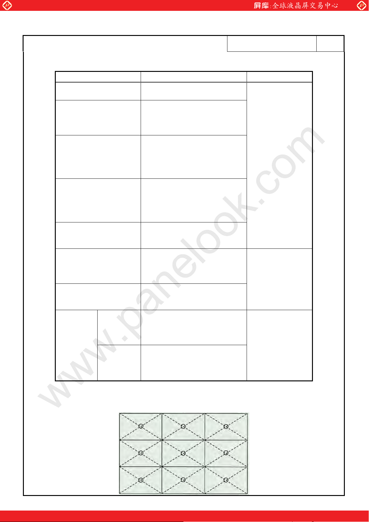
7. RELIABILITY TESTS
Test item Condition Judgement Note1
High temperature and
humi ion)
dity(Operat Display data is blackĸ
Heat cycle
(Operation) s/cycle
Thermal shock
(Non operation)
ESD
(operation)
Dust
(operation)
Vibration
(Non operation)
echanical shock
M
(Non operation)
Low pressure
non-operation
Note1: Display mental conditions equivalent to the inspection
and appearance are checked under environ
conditions of defect c
Note2: See the following figure for discharge points.
opera
tion
50±2 ,RH=85%,240hoursķć
0±3 ...1hourķć
55±3 ...1hourć
50cycles,4hourĸ
Display data is bl
ķ -20±3 ...30mić nutes
60±3 ...30minutesć
100cycles,1hour/cycleĸ
Temperature transiti
within 5 minutes.
150Pf,150,±10kVķ
9 places on a
Note2
10 times each places at 1 sec Ĺ
int
erval
Sample dust: No.15(byķ JIS-Z8901)
15 seconds stirĸ
8 times repeat at 1 hour intervalĹ
5ķ -100Hzˈ11.76
1 minutes/cycleĸ
X,Y,Z directionĹ
50 times each dirĺ
294m/Sķ
±Xĸ ˈ±Yˈ±Z direction
3 times each direcĹ
53.3kPa (Equivalent toķ
4,850m˅
0 ±3 ...24hoursĸć ć
50 ±3 ...24hoursćć
Ĺ
ķ 15kPa (Equivale
13,600m˅
ĸ -20ć±3ć...24hours
60ć±3ć...
Ĺ 24hours
2
ˈ11ms
ackĹ
on time is Ĺ
panel surface ĸ
2
m/S
ections
tions
altitude
nt to altitude
riteria.
SN-SA-A0001-01-E 29/38
No display
malfunctions
No display
malfunctions
No p ges
hysical dama
No display
malfunctions
Shanghai SVA NEC Liquid Crystal Display Co., Ltd.
One step solution for LCD / PDP / OLED panel application: Datasheet, inventory and accessory!
www.panelook.com
Page 30
Global LCD Panel Exchange Center
www.panelook.com
SN-SA-A0001-01-E 30/38
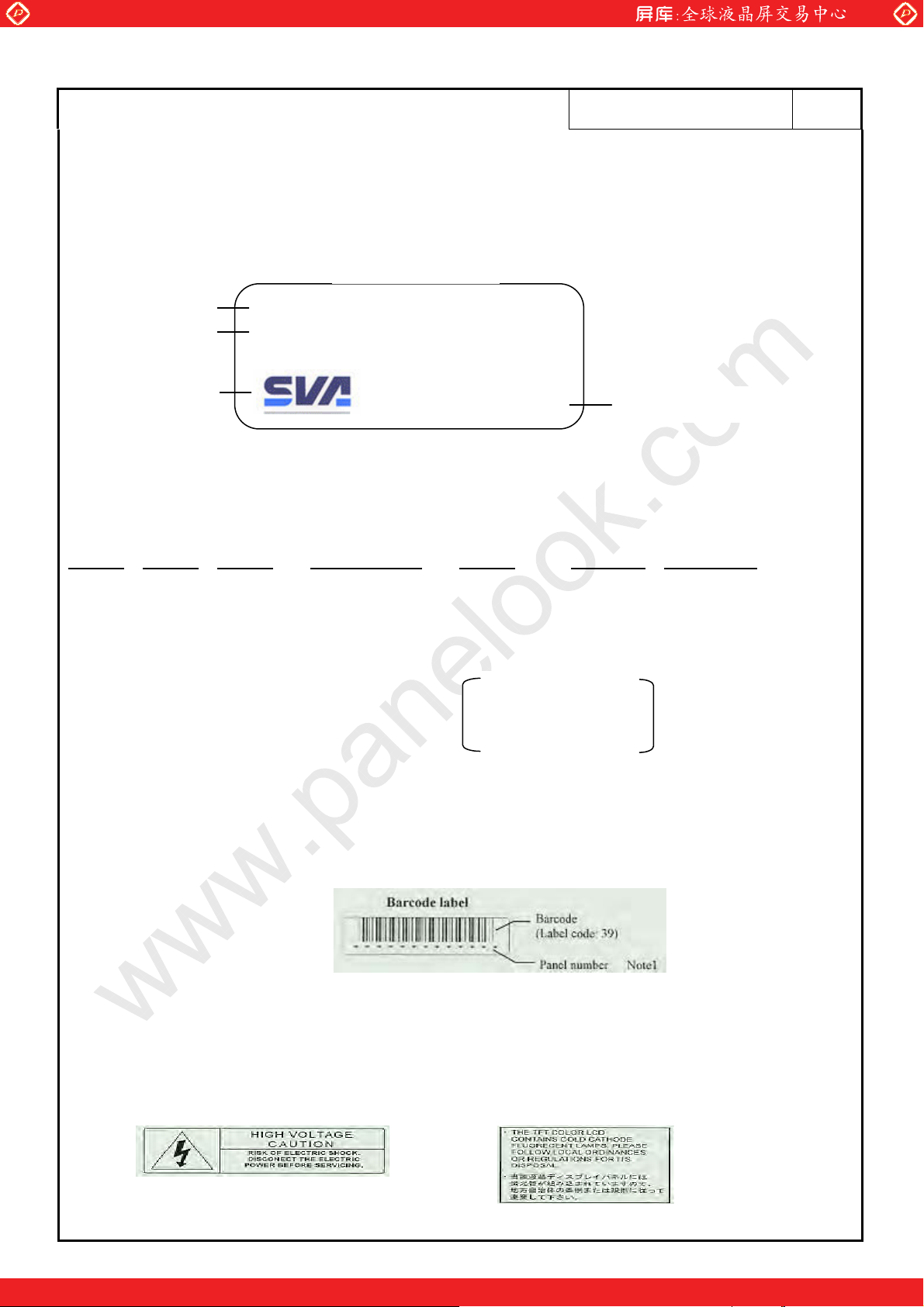
8. MARKINGS
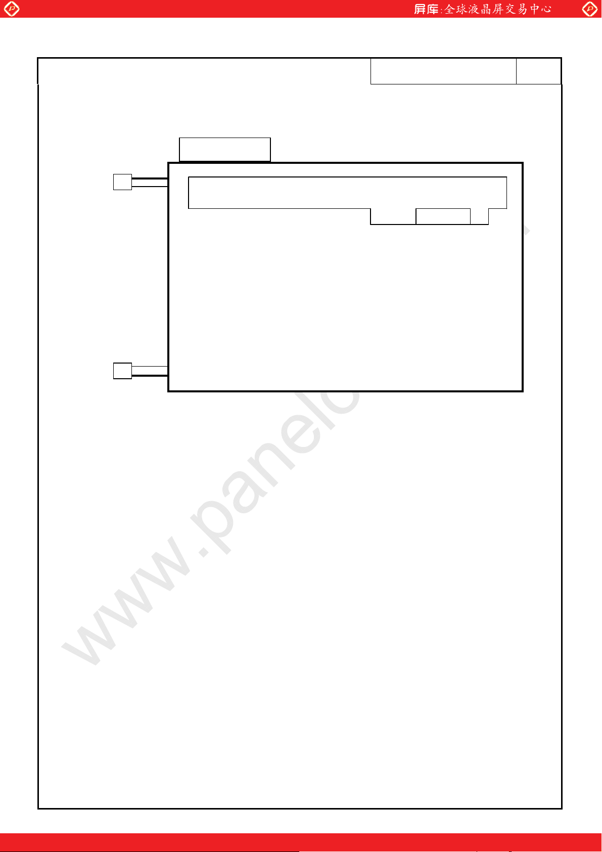
The various markings are attached to this product. See “8.4 INDECATION LOCATIONS” for
attachment positions.
8.1 NAMEPLATE LABEL
Note1
Ty
pe name
Lot number
Company emblem
MODEL: SVA150XG01TB
LOT NO: 111A004201001
CELL ID: A2013Z2909012
Name plate label
MADE IN CHINA
Note2
ntry of manufacture
Cou
Note1: The meaning of lot number
111A004201001
噝Example:
$
Internal Revision
use 1
letter
(Alphabet)
Internal Manufacturing
use
2 figures of the A.D.
end numbers 1 lette
(e.g: A.D2004 is 04.)
year
Manufacturing
month
r
o Sep.: N
Jan. t umber of month
October: A
November: B
December: C
Note2: Do not attach anything such as label and so on, on the nameplate! In ca
produc NE the ts h a be d on, to
identify the warranty period with individual product. If SV C cannot decipher the contents of
nameplate, such all be entitled . Also S C may give a new lot number to
t, SVA- C needs conten of nameplate suc s the lot num
A-NE
repair sh to charge VA-NE
Manufacturing Production
day number
tter
Multi-le
(figure)
se repair the
r, inspection ate and so
reconditioned products.
8.2 BARCODE LABEL
Note1: the same panel number is given to barcode label and nameplate label.
8.3 OTHER MARKINGS
High voltage caution marking Disposal method marking for lamp
Shanghai SVA NEC Liquid Crystal Display Co., Ltd.
One step solution for LCD / PDP / OLED panel application: Datasheet, inventory and accessory!
www.panelook.com
Page 31
Global LCD Panel Exchange Center
www.panelook.com
,1',&$7,21/2&$7,21
Product rear side
High voltage caution
SN-SA-A0001-01-E 31/38
6
Disposal method marking Barcode label Nameplate label
Shanghai SVA NEC Liquid Crystal Display Co., Ltd.
One step solution for LCD / PDP / OLED panel application: Datasheet, inventory and accessory!
www.panelook.com
Page 32
Global LCD Panel Exchange Center
www.panelook.com
SN-SA-A0001-01-E 32/38
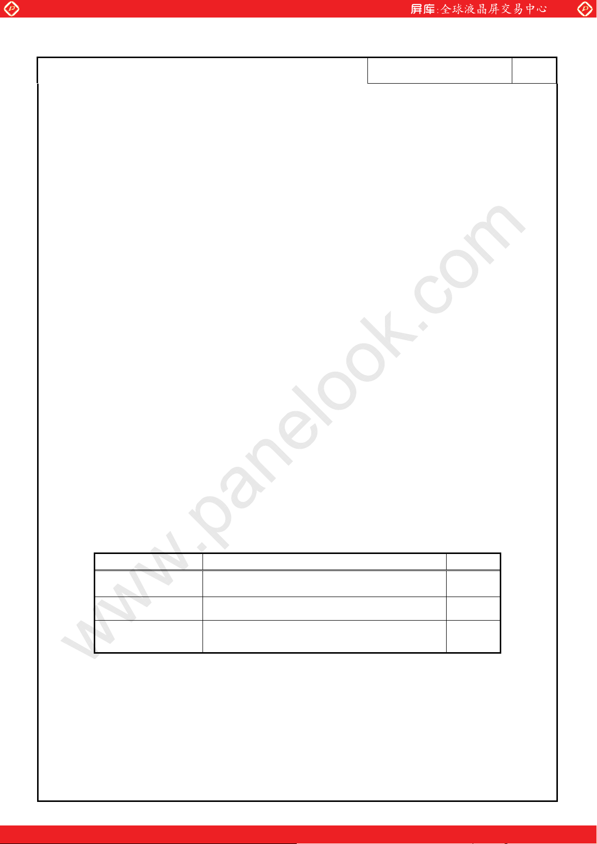
9. PACKING, TRANSPORTATION AND DELIVERY
SVA-NEC will pack products to deliver to customer in accordance with SVA-NEC packing specifications, and will
d
eliver products to customer in such a state that products will not suffer from a damage during transportation .The
d
elivery conditions are as follows.
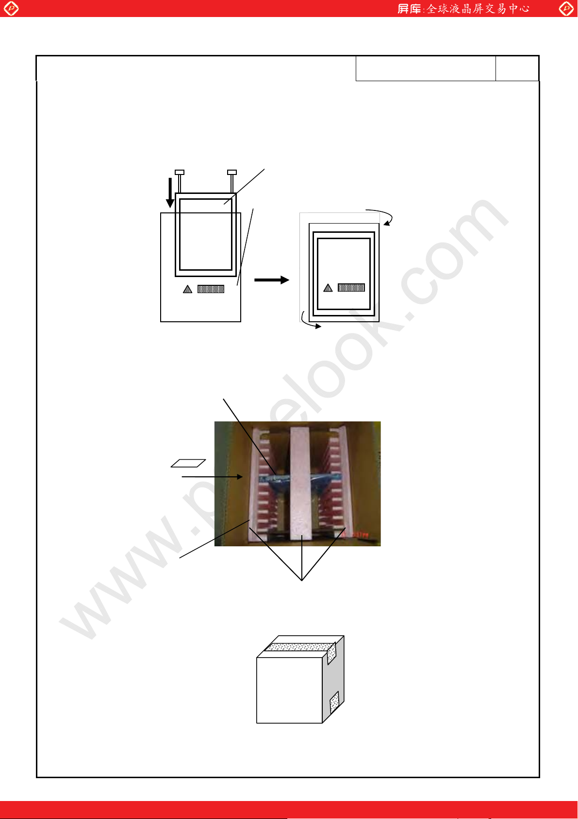
9.1 PACKING
(1) Packing box
10 products are packed up with the maximum in a pa
PACKING “).
Products are put into a plastic bag for prevention of moisture with cushion, and then the bag is sealed up with
heat sealing
The type name and quality
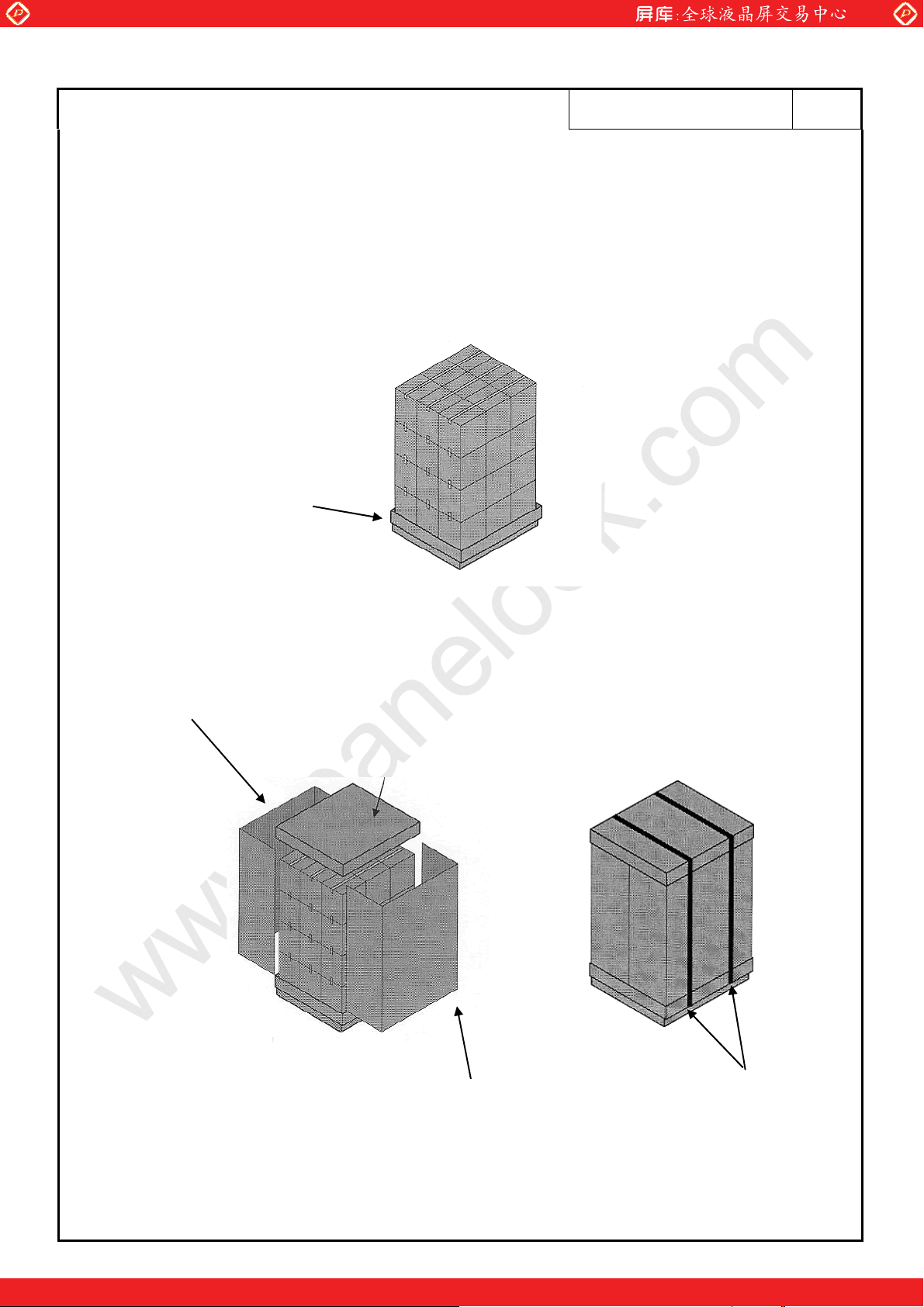
)Pallet Packing (See” 9.5 OUTLINE FIGURE FOR PACKING “)
(2
ķ Packing boxe
ĸCardboard sleeve and top cap are attached to the packing boxes, then they are fixed by a band.
.
are shown on outside of the packing box, either labeling or printing.
s are tired on a cardboard pallet.(9 boxes×4 tiers maximum)
cking box(See “9.5 OUTLINE FIGURE FOR
9.2 INSPECTION RECORD SHEET
Inspection record sheets are included in the packing box with delivery products to customer. It is summarized to a
nu cts for pass/fail assessment.
mber of produ
9.3 TRANSPORTATION
The product is transported by vehicle, aircraft or shipment in the state of pallet packing.
9.4 SIZE AND WEIGHT FOR PACKI
NG BOX
Parameter Packing box Unit
Size
Weight
Total weight
374˄L˅x 319˄W˅x 470˄H˅˄typ.˅
1.6˄ty
11.3˄typ.˅
(w
ith 10 products)
p.˅
mm
kg
kg
Shanghai SVA NEC Liquid Crystal Display Co., Ltd.
One step solution for LCD / PDP / OLED panel application: Datasheet, inventory and accessory!
www.panelook.com
Page 33
Global LCD Panel Exchange Center
g
www.panelook.com
9.5 OUTLINE FIGURE FOR PACKING
(1) Packing box
SV
A
SN-SA-A0001-01-E 33/38
LCD module
Antistatic pouch
SVA
LCD module
Inspection record
sheet
Plastic bag for prevention
of moisture
Cushion
Packi
One step solution for LCD / PDP / OLED panel application: Datasheet, inventory and accessory!
bo
n
x
Shanghai SVA NEC Liquid Crystal Display Co., Ltd.
www.panelook.com
Page 34
Global LCD Panel Exchange Center
p
www.panelook.com
SN-SA-A0001-01-E 34/38
Pallet packing
Note: The ways for Packing and Shipping vary from different shipment volume, dependent on
specific situations.
Cardboard pallet
ng boxes (9 boxes×4 tiers maximum)
Packi
Cardboard sleeve
Top ca
Cardboard sleeve
Band
Shanghai SVA NEC Liquid Crystal Display Co., Ltd.
One step solution for LCD / PDP / OLED panel application: Datasheet, inventory and accessory!
www.panelook.com
Page 35
Global LCD Panel Exchange Center
www.panelook.com
10. PRECAUTIONS
SN-SA-A0001-01-E 35/38
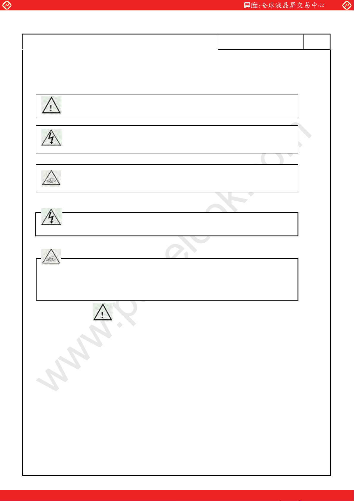
10.1 MEANING OF CUTION SIGNS
The following caution signs have very important m g .Be sure to read “10.2 CAUTIONS” and “10.3
ATTENTIO tanding these contents!
sustain a damage, if customer has wrong operations.
NS”, after unders
gn have the meanin tomer will be injured by himself or the product will
This si
g that cus
eanin
This sign has the meaning that customer will get an electrical shock, if customer has
wrong operations.
This sign has the meaning that customer will be injured by himself, if customer has
wrong operations.
10.2 CAUTIONS
Do not touch lamp cables while turn on .Customers will be in danger of an electric shock
Do not touch the working backlight and IC. Customers will be in danger of burn injury.
Do not shock and press the LCD panel and the backlight! There is a danger of breaking,
because they are made of glass.(shock :To be not greater 294m/s
11ms, Pressure:
To be not greater 19.6N)
2
and to be not greater
10.3 ATTENTIONS
10.3.1 Handling of the product
ķ Tak hold of both ends without touch the circuit board when customer pulls out products (LCD modules) from
ĸ Do not hook cables nor pull connection cables such as flexible cable and so on , for fear of damage.
Ĺ If customer puts down the product temporarily, the product puts on flat subsoil as a display side turns do
ĺ asures of electrostatic discharge such as earth band, ionic shower and so on, when custTake the
ĻThe torque for mounting screws must never exceed 0.34N-m. Higher torque values might result in distortion of the
ļ ct must be installed using mounting holes without undue stress such as bends or The prod
Bends or twist described above and undue stress to any portion except mounting hole portion may cause display
ĽDo
e
inner packing box. If customer touches it, products may be broken down or out of adjustment, because
mounting parts.
me omer deal with
the produ may be damaged by electrostatic.
bezel.
drawings due stress to any portion (such as bezel flat area) except mounting hole portion.
un-uniformity.
using the
ct, because products
u twist (See outline
).And do not add un
not press or rub on the sensitive display surface .If customer clean on the panel surface, SVA-NEC recommends
cloth with ethanolic liquid such as screen cleaner for LCD.
Shanghai SVA NEC Liquid Crystal Display Co., Ltd.
of stress to
wn.
One step solution for LCD / PDP / OLED panel application: Datasheet, inventory and accessory!
www.panelook.com
Page 36
Global LCD Panel Exchange Center
www.panelook.com
ľ Do not push-pull the interface connectors while the product is working, because wrong power seq
down the product.
ĿDo not bend or unbend the lamp cable at the near part of the lamp holding rubber, to avoid the dama
voltage
side of the lamp. This damage may cause a lamp breaking and abnormal operation of high voltage circuit.
SN-SA-A0001-01-E 36/38
uence may break
ge for high
10.3.2 Environment
not operate or store in high temperature,
ķ Do high humidity, dewdrop atmosphere or corrosive gases. Keep the
product in antistatic pouch in room temperature, because of avoidance for dusts and sunlight, if customer stores
the product.
In order to prevent dew condens
ĸ ation occurring by temperature difference, the product packing box must be
opened after leave under the environment of an unpacking room temperature enough. Because a situation of dew
condensation occurring is changed by the environment temperature and humidity, evaluate the leaving time
sufficiently. (Reco
ĹDo not operate in a high magnetic field .Circuit boards may be broken down by it.
ĺThis product is not designed as radiation hardened.
ĻUse an original protection sheet on the product surface (polarizer). Adhesive type protection sheet should be
avoided, because it may change color or properties of the polariz
mmendation leaving time: 6 hour or more with packing state)
er.
10.3.3 Characteristics
The following items are neither defects nor failures.
ķ
Response time, luminance and color may be changed by ambient temperature.
ĸThe LCD may be seemed luminance non-uniformityflicker, vertical seam or small spot by display patterns.
Ĺ eristics (e.g. luminance, display uniformity, etc.) gradually is going to change depending on
Optical charact
operating time ,and especially low temperature, because the LCD has cold cathode fluorescent lamps.
ĺ e image sticking .Use a screen saver, if the
Do not display the fixed pattern for a long time because it may caus
fixed pattern is displayed on the screen.
ĻThe display col
ļOptical characteristics may be changed by input signal timings.
ĽThe interference noise of input signal frequency for this product and luminance control frequency of custom
backlight inverter may appear on a display. Set up luminance control frequency of backlight inverter so that the
interference noise dos
or may be changed by viewing angle because of the use of condenser sheet in the backlight.
er’s
es not appear.
10.3.4 Other
ķ
All GND and VCC terminals should be used without a non-connected line.
ĸ emble a product or adjust volume without permission of SVA-NEC.
Do not disass
ĹSee “REPLACEMENT MANUAL FOR LAMPHOLDER SET”, if customer would like to replace backlight
lamps.
ĺ
Pay attention not to insert waste materials inside of products, if customer uses screw nails.
Ļ damages during transportation,
Pack the product with original shipping package, because of avoidance of some
when customer returns it to SVA-NEC for repair and so on.
ļNot only the module but also the equipment sh
vertical .Otherwise, there is the fear that a display dignity decreases by an impact or vibrations.
ould be packed and transported as the module. becomes
Shanghai SVA NEC Liquid Crystal Display Co., Ltd.
One step solution for LCD / PDP / OLED panel application: Datasheet, inventory and accessory!
www.panelook.com
Page 37
Global LCD Panel Exchange Center
www.panelook.com
One step solution for LCD / PDP / OLED panel application: Datasheet, inventory and accessory!
www.panelook.com
Page 38
Global LCD Panel Exchange Center
www.panelook.com
One step solution for LCD / PDP / OLED panel application: Datasheet, inventory and accessory!
www.panelook.com
 Loading...