

Page 1

EPFL Swiss Institute of Technology Lausanne Page 1
CMi Center of MicroNanoTechnology
Süss MJB4 Mask Alig ner Use r Manual
Version of 8.10.2016. Get the latest one at http://cmi.epfl.ch/photo/files/MJB4/MJB4.std.manual.pdf
1. Introduction
This user manual explains how to operate the
Süss MJB4 mask-aligner. Default illumination
setup on MJB4: Intensity = 20mW/cm
2
, i-line
(365nm) illumination.
2. Login & System Initializ ati on
• Login on “SussMicroTec MJB4 …” with CAE on
zone 13 accounting computer.
• Check if the main power switch is turned on. If
not, turn it on.
• Before starting with the machine, users should
check that the mercury (Hg) lamp is on. Note
that the lamp will be automatically turned off 45
minutes after the last user logs out.
• Check the lamp power supply (CIC):
If the lamp is on, CP button LED will be on
and you will be able to read light intensity
(0.0) and lamp power values. Continue to
the next section.
If the lamp is off, the CIC power supply will
be either off or show “Standby”. If the touch
panel displays “start maschine with
ON/OFF button”, then press the ON/OFF
button on the left front panel. The CIC will
turn on.
Then use the following sequence to start
the lamp:
Display Standby Press “On”.
Display Ready Press “CP”.
Display Start Press “Start”.
The display will show blinking "co ld". Wait
at least 10 minutes before exposure to
make sure the lamp temperature is stable!
• Reset wafer & chuck positioning/travel range by
adjusting the following :
Center position for x-axis (knob to 10)
Center position for y-axis (knob to 10)
Center position for θ angle
Chuck rotation at “zero”
x-axis
y-axis
θ-axis
chuck rotation
θ-axis
Page 2

EPFL Swiss Institute of Technology Lausanne Page 2
CMi Center of MicroNanoTechnology
3. Preparation: Mask Loading
• Unclamp the mask holder with the 2 screws on
the right side of the frame.
• Take the mask holder out of the frame, rotate it
and put it on the small table left side of the
MJB4.
• Fit properly the mask on the mask holder by
contacting the three metal pins.
• On the MJB4 touchscreen, go in the “Main
Menu” section. Press «Mask vacuum is off» to
turn on vacuum clamping. Verify that the mask
does not move.
• Put the mask holder with the mask back into
the MJB4. Clamp the mask holder with the 2
screws. Make sure it is sufficiently fixed.
4. Preparation: Exposure Re cipe
• Calculate your optimal exposure time,
according to the recommended exposure dose
given on the CMi website and the lamp
intensity. Default illumination setup on MJB4:
Intensity = 20mW/cm
2
, i-line (365nm)
illumination.
• On the MJB4 touchscreen, press “Parameters”
to access the exposure settings.
• Select the exposure mode under number 1):
“Align + Exp.” = standard mode.
“Flood Exp.” = no mask, full wafer
exposure.
“Test Exp.” = to expose the wafers
several (defined by the “exposure cycles”
parameter) times with different exposure
times.
• Select the contact mode under number 2):
“Hard Contact” = standard mode.
“Soft Contact” = for fragile wafers or
extremely thick resist.
“Vacuum Contact” = NOT AVAILABLE on
MJB4.
*Gap Exposure” = to expose with a gap
between wafer and mask (proximity).
• Set-up the rest of the parameters
Hard Contact time: 10s
Exposure time: “x” (calculated before)
Exposure cycles: 1
• To perform split-exposure, change the
“Exposure cycles” parameter to any values
higher than 1. “Wait time” parameter will show
up below.
• Once the recipe parameters are set, press the
“Load” key to save your parameters.
• Make sure that the CIC mode is set to constant
power (CP). The use of other exposure modes
is not recommended with the MJB4 maskaligner.
5. Preparation: WEC setti ngs
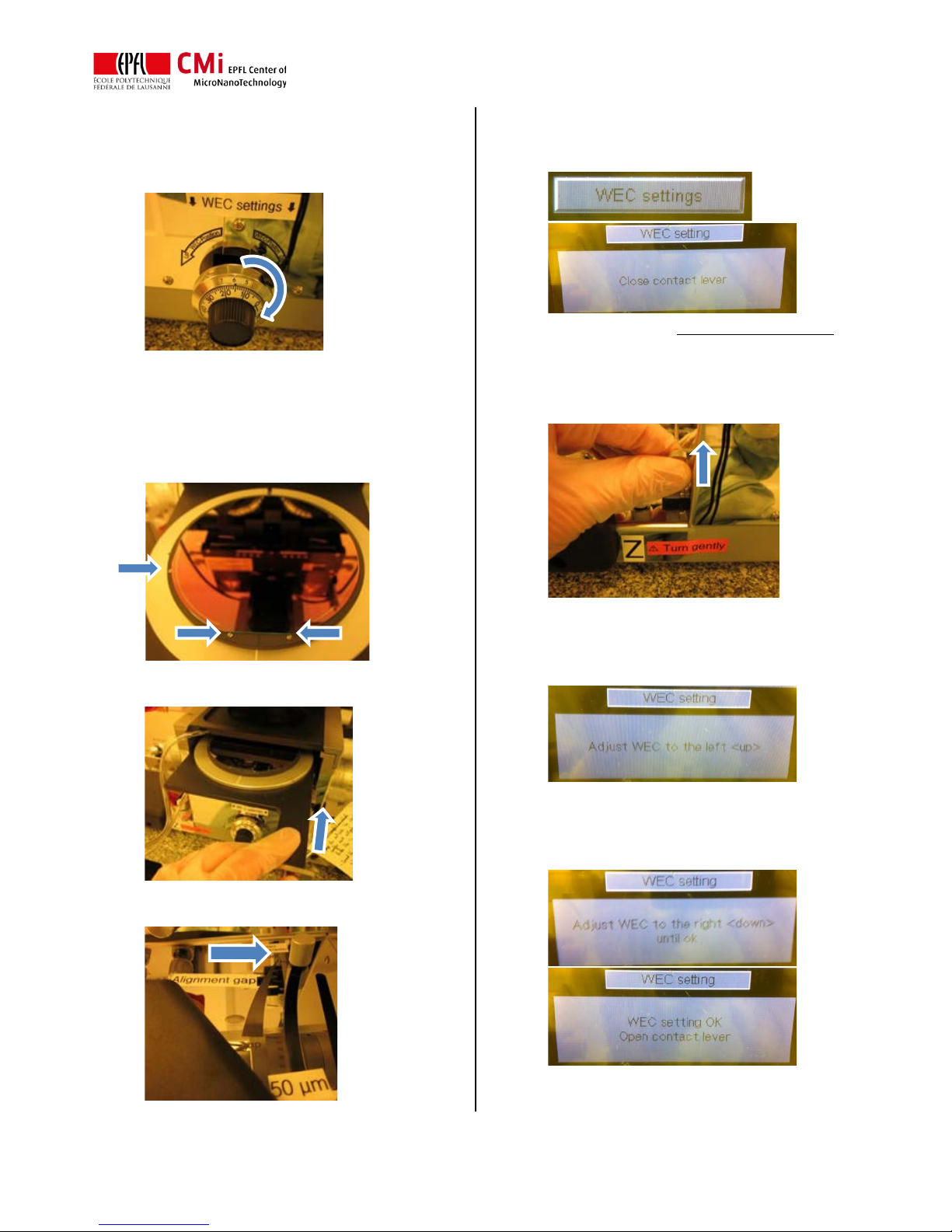
On the MJB4, the wedge error compensation
(WEC) procedure for fine tuning of mask/wafer
contact position and parallelism is done manually.
Follow this procedure:
• Before starting check that WEC pressure
setting is higher than 0.05 MPa! If it is lower
please adjust with the appropriate knob (front
panel, right of the machine).
Page 3
EPFL Swiss Institute of Technology Lausanne Page 3
CMi Center of MicroNanoTechnology
• Rotate WEC knob down (to the right) for
adequate wafer to mask clearance. Position
should be “0” when using a Cr-blank mask, or
“16” when using a transparent sheet mask.
Note: each unit on the scale is 1 µm. One full
rotation to the right moves the WEC offset
down by 100 µm.
• Pull the wafer slide and place the wafer in
contact with the three positioning pins. Be sure
not to load on top of the pins!
• Activate the wafer transport vacuum and push
the slide at the back of the machine.
• Make sure that the “alignment gap” lever is at
the upper position (Contact mask/wafer).
• At this point, press “WEC settings” on the
touchscreen and wait for the message “Close
contact lever”.
• Turn the contact lever slowly and very gently
until the end the position is reached (manual zaxis). Do not force it if you feel some
resistance. ! The WEC unit might be too high,
check the display for errors !
• Now, follow directions of rotation given on the
display. First rotate the WEC up (to the left).
For standard thin resists, contact position will
be around “16”.
• Then the display will ask “Adjust WEC to the
right <down> until ok”. Rotate the WEC to the
right until you get the following message: “WEC
setting OK”.
• To complete the WEC procedure, take the
contact lever to “starting” position. The display
Page 4

EPFL Swiss Institute of Technology Lausanne Page 4
CMi Center of MicroNanoTechnology
will turn back to the main menu.
6. Alignment & Exposure
• Once the WEC procedure is done, the MJB4 is
ready for alignment & exposure. Load the wafer
in contact with the three positioning pins, and
push the slide at the back of the machine.
• Make sure that the “alignment gap” lever is at
the upper position (Contact mask/wafer).
• Turn the contact lever slowly and very gently to
move the wafer up to contact position. The
display will switch to “Exposure menu” and
show three options:
• Alignment check: to perform hard-
contact before exposure and check
alignment accuracy.
• Exposure: to expose directly (first mask
exposure).
• Parameters: to modify the exposure
parameters.
• To perform a top-side alignment (TSA), make
sure that microscope illumination is on (knobs
turned fully right).
• Use the binoculars or the TV screen display to
visualize the mask. Make sure “SPLITFIELD”
mode is activated on the microscope (see [7]
below) to see both right and left field of view.
• Move the left and right objectives on top of your
alignment markers on the mask and adjust the
focus.
Top microscope controls:
= x- / y- stage movement
= Theta axis / rotation
= intra-objective distance (one on each
side)
= Coarse z-axis / focus (one on each side)
= fine objective focus (one on each side)
= illumination attenuation (one on each
side)
= Splitfield mode
= Screen or binocular view
= objectives turret (manual change)
• Before moving the wafer, separate mask and
wafer using the alignment gap lever. Taking the
lever completely down will move the wafer
Page 5

EPFL Swiss Institute of Technology Lausanne Page 5
CMi Center of MicroNanoTechnology
down to an alignment gap of about 50 µm.
• Move the wafer using x-axis , y-axis and θ-axis
knobs in order to find the markers on the wafer.
• Move the wafer markers under the mask
markers. Alig n precisely horizontal features on
the right and left fields using the y-axis and θaxis knobs.
• Finish the alignment with fine-tuning of the xaxis.
• When alignment is done, move the wafer back
in contact using the alignment gap lever.
• On the MJB4 touchscreen, pressing “Alignment
check” will perform the selected contact
procedure (hard, soft). If alignment is good,
move on with “Exposure”.
• Pressing “Exposure” and confirming with “YES”
will perform the exposure.
• Wait for the end of the exposure procedure,
open the contact lever and pull the slide to
unload the wafer.
• Repeat the loading-exposure-unloading loop to
complete your wafer batch.
• To unload the mask, proceed the opposite way
you already did for mask loading (see section
3).
• Move the mask holder slide into the machine
and logout with CAE on zone 13 accounting
computer.
 Loading...