

Page 1
DDeellaayylliinnee DDeetteeccttoorr DDLLDD 88008800
Delayline Detector
DLD 8080
Manual
Page 2

DDeellaayylliinnee DDeetteeccttoorr DDLLDD 88008800
2
Page 3

DDeellaayylliinnee DDeetteeccttoorr DDLLDD 88008800
3
A
ll rights reserved. No part of this
manual may be reproduced without the
prior permission of Surface Concept
GmbH.
Surface Concept GmbH
Am Sägewerk 23a
55124 Mainz
Germany
Tel. ++49 6131 62760
Fax: ++49 6131 6271629
www.surface-concept.com,
support@surface-concept.de
Manual Version: 1.2
Date: 2010-05-10
Page 4

DDeellaayylliinnee DDeetteeccttoorr DDLLDD 88008800
4
Page 5

DDeellaayylliinnee DDeetteeccttoorr DDLLDD 88008800
5
1 Table of Contents
1 Table of Contents.................................................................................................................................................................................. 5
2 Introduction.............................................................................................................................................................................................. 8
2.1 General Information................................................................................................................................................................... 8
2.2 Safety Instructions...................................................................................................................................................................... 8
2.3 General Overview of the System .......................................................................................................................................... 9
3 Installation .............................................................................................................................................................................................10
3.1 Initial Inspection ........................................................................................................................................................................10
3.2 Installation ................................................................................................................................................................................... 11
3.2.1 Mounting the delayline detector.............................................................................................................................. 11
3.2.2 Detector Orientation ....................................................................................................................................................11
3.2.3 Cabling and High Voltage............................................................................................................................................ 12
3.2.4 Recommended System Requirements................................................................................................................ 14
4 USB 2.0 Driver Installation ............................................................................................................................................................ 15
5 DLD - Principle of Operation .......................................................................................................................................................... 18
5.1 Basics of Delayline Detection.............................................................................................................................................. 18
5.2 Basic Operational Modes of the Delayline Detector ................................................................................................ 19
5.2.1 2D(x, y) Area Detection ............................................................................................................................................... 19
5.2.2 3D(x, y, t) time resolved imaging............................................................................................................................. 19
5.3 Data Acquisition........................................................................................................................................................................ 20
5.4 Working with the DLD – Important details .................................................................................................................. 20
6 Delayline Detector Layout ..............................................................................................................................................................21
Page 6

DDeellaayylliinnee DDeetteeccttoorr DDLLDD 88008800
6
6.1 Delayline Detector - Vacuum Wiring............................................................................................................................... 21
6.2 Delayline Detector – Connection Ports ......................................................................................................................... 22
7 Pulse Processing Electronics ....................................................................................................................................................... 24
7.1 Pulse Processing Electronics ACU 3.4.2...................................................................................................................... 24
7.1.1 Positions of the Discriminator Threshold Regulators................................................................................... 25
8 Time-to-Digital-Converter (TDC) ................................................................................................................................................... 26
8.1 Schematic Description of the USB2.0-TDC .................................................................................................................26
8.2 Basic Operation Modes of the GPX TDC Chip............................................................................................................. 27
8.2.1 I-Mode (USB2.0-TDC/ Double USB2.0-TDC )................................................................................................... 27
8.2.2 R-Mode (High Resolution/ Dual Channel/ Quad Channel USB2.0-TDC) ............................................. 27
8.2.3 G-Mode (High Resolution/ Dual Channel/ Quad Channel USB2.0-TDC) ............................................. 27
8.3 Layout of the Quad Channel USB2.0-TDC..................................................................................................................... 28
8.3.1 TDC Inputs (Stop + Start)........................................................................................................................................... 28
8.3.2 Trigger Synchronization IN/OUT............................................................................................................................ 28
8.3.3 Line Input ........................................................................................................................................................................... 29
8.4 Interface (PC) and Software................................................................................................................................................ 29
9 Dual HV Supply............................................................................................................................................................................. 30
9.1 Layout of Dual HV Supply & the HV filterbox................................................................................................................ 31
9.1.1 Line Input of Dual HV Supply .....................................................................................................................................32
9.2 Connection schemes for different operation modes............................................................................................... 32
10 Operation of the DLD................................................................................................................................................................... 36
10.1 Getting Started ....................................................................................................................................................................36
10.2 Turning on the High Voltage........................................................................................................................................... 36
10.2.1 “Start-Up” Procedure (for new systems and for systems, after being vented).............................37
10.2.2 Standard Start Procedure.................................................................................................................................... 38
10.3 Bake Out Procedure.......................................................................................................................................................... 39
11 Microchannel Plate (MCP)........................................................................................................................................................ 40
11.1 Storage.................................................................................................................................................................................... 40
11.2 Handling .................................................................................................................................................................................. 40
Page 7

DDeellaayylliinnee DDeetteeccttoorr DDLLDD 88008800
7
11.3 Operation................................................................................................................................................................................ 41
12 Technical Data .............................................................................................................................................................................. 42
13 List of Figure....................................................................................................................................................................................43
Page 8

DDeellaayylliinnee DDeetteeccttoorr DDLLDD 88008800
8
2 Introduction
2.1 General Information
This manual is intended to assist users in the installation, operation and maintenance of the Delayline
Detector DLD 8080. It is divided into 13 chapters. The chapter “Introduction” contains a brief description of
the DLD. The chapter “Installation” refers to installation and cabling. One chapter describes the USB driver
installation. Chapter “Principle of Operation” explains the theory of operation of the DLD. 3 chapters describe
the technical details of the detector readout package and chapter “Operation of the DLD” describes the
operation of the DLD. The final chapters contain amongst others, technical details about the microchannel
plates and the delayline detector in general.
2.2 Safety Instructions
Please read this manual carefully before performing any electrical or electronic operations and strictly
follow the safety rules given within this manual.
The following symbols appear throughout the manual:
The “note symbol” marks text passages, which contain important information/ hints
about the operation of the detector. Follow these information to ensure a proper
functioning of the detector.
The “caution symbol” marks warnings, which are given to prevent an accidentally
damaging of the detector or the readout system. Do NOT
ignore these warnings and
follow them strictly
. Otherwise no guarantee is given for arose damages.
The “high voltage symbol” marks warnings, given in conjunction with the description of
the operation/ use of high voltage supplies and/ or high voltage conducting parts.
Hazardous voltages are present, which can cause serious or fatal injuries. Therefore
only persons with the appropriate training are allowed to carry out the installation,
adjustment and repair work.
Page 9

DDeellaayylliinnee DDeetteeccttoorr DDLLDD 88008800
9
2.3 General Overview of the System
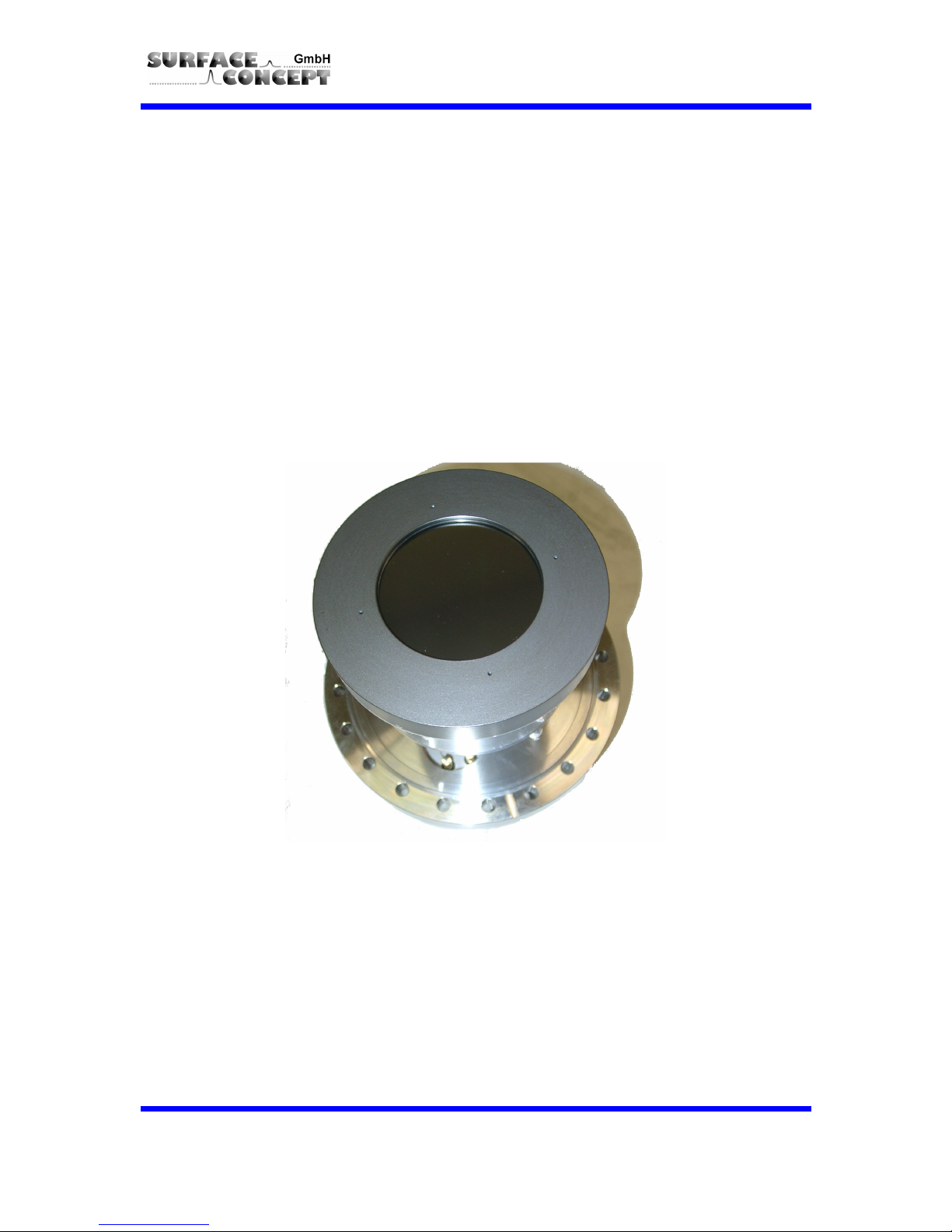
The Surface Concept delayline detectors are particularly developed for the needs of 1D(x), 2D(x,t), 2D(x,y) or
3D(x,y,t) area and time detection of electrons, ions, x-ray and UV-light as well as for multi hit detection of high
rates with the 4-quadrant detector systems.
The DLD 8080 is mounted on a CF 150 vacuum flange with feed-throughs for high voltage supply and signal
transfer. It consists of a microchannel plate stack and two layers (x, y) of meander structured delaylines. The
image is sampled by the DLD readout electronics.
The 3D (x, y, t) detection bases on the measurement of time differences and time sums of signals, with a high
temporal resolution in one device. The count rate can reach up to 2.0 MHz in the commonly used 4-fold
coincidence measurement.
Typical applications are for example:
• imaging of parallel incident particle beams, particularly electrons
• spatially resolved time of flight spectroscopy in 2D/time resolved mode
• time referenced imaging of electrons excited by repetitive driven sources
and in energy analyzers:
• Fermi surface mapping, band mapping, photoelectron diffraction measurements, and similar angular
dispersion experiments in 2D mode
• XPS, UPS, ESCA and AES in virtual channel mode
• Stroboscopic experiments in 2D/time resolved mode
Page 10

DDeellaayylliinnee DDeetteeccttoorr DDLLDD 88008800
10
3 Installation
3.1 Initial Inspection
Visual inspection of the system is required to ensure that no damage has occurred during shipping. Should
there be any signs of damage, please contact SURFACE CONCEPT immediately. Please check the delivery
according to the packing list (see Table 1) for completeness.
1. Dual HV Supply
2. Quad Channel USB 2.0–TDC with USB2.0 cable
3. Delayline Detector DLD8080 under vacuum
4. HV filterbox
5. Pulse processing unit ACU 3.4.2
6. 2x SHV cables (5m),
7. 1x SHV cable (approx. 10 cm)
8. 1x SHV termination plug
9. 1x DLD readout cable (HDMI)
10. Documentation and Software (CD)
Table 1: Packing list for the Delayline Detector
Figure 1: Contents of delivery package
1
2
3
10
5
4
67
8
9
Page 11
DDeellaayylliinnee DDeetteeccttoorr DDLLDD 88008800
11
3.2 Installation
3.2.1 Mounting the delayline detector
The detector is transported under vacuum. Vent the transport container carefully and release the M8
screws of the vacuum container and pull out the detector carefully
.
Check the front side of the MCP stack for particles.
The microchannel plates in front of the detector should be protected from exposure to
particle contamination. Particles that stick to the plate can be removed by carefully using
a single-hair brush carefully and/or with dry nitrogen. Reading the instructions
“microchannel plates” in chapter 11 is strongly recommended.
Install the detector to your vacuum chamber.
The DLD needs a tube with a diameter of minimum 160 mm, to be installed to.
The max. outer diameter of the detector housing is 147mm. The housing is connected to
the MCP front potential. Due to isolation distances (detector housing potential can reach
more than 4000 V) the min. diameter of the tube, where the detector is installed to, must
be of at least 160mm.
Keep the transport container in case that the detector must be sent back for repair. It can also be used to
store the detector when not installed in a vacuum chamber.
The detector should be kept under vacuum all the time.
3.2.2 Detector Orientation
The black dot in Figure 2 marks the 0/0 position of the DLD image, which corresponds to the upper left
corner of the DLD image in the GUI software.
Page 12

DDeellaayylliinnee DDeetteeccttoorr DDLLDD 88008800
12
Figure 2: 0/0 position of the DLD image (black dot).
3.2.3 Cabling and High Voltage
The general connection scheme of the delayline detector including its readout package is shown in Figure 3.
Figure 3: Connection scheme of the delayline detector and readout package.
• The pulse processing unit ACU can be connected directly to the DLD 4-fold SMB feed-through. The
metal pin gives the orientation. Fasten the ACU with the two clips on the housing.
• Use the DLD readout cable to connect the “Lines Out” socket on the front of the ACU with the “TDC
Input” socket at the rear panel of the USB2.0-TDC. To perform time measurements with respect to an
external clock, provide start pulses to the start input of the TDC. Use the BNC socket named “TTL
Page 13

DDeellaayylliinnee DDeetteeccttoorr DDLLDD 88008800
13
Start” to apply standard TTL signals.
The start input of the TDC is not working with start signals of frequencies smaller 25 kHz and
larger than 7 MHz.
Larger start pulse frequencies must be divided down with an appropriate frequency divider (e.g.
divider with factor of 16 for 80 MHz start pulse frequency).
• There is a CF40 flange with 2 SHV feed-throughs for high voltage supply of the detector. The
connection of the feed-throughs is as follows:
MCP front (F) and detector anode (A)
The Dual HV Supply holds 6 SHV connectors labeled A, REF A, F, REF F, B+ and B-.
The connectors A and F must always be connected to the corresponding SHV feed-through of the DLD
with the HV filterbox in between.
Do not operate the DLD without the HV filterbox.
This will lead to a significant decrease in the image quality.
The operation voltage for the DLD (specified in the specification sheet) is always applied between A and
F. It is produced by the HV module “HV A”.
REF A and REF F are connected to A and F respectively. They allow connecting a reference potential to
the one or other side of the MCP stack. The DLD can be operated floating on a bias voltage (positive or
negative). The HV module “HV B” can be used to generate this bias voltage.
For the first tests the detector should be operated with the following HV connection:
• Connect the 2 SHV connectors A & F of the Dual HV Supply with the corresponding inputs of the
HV Filterbox.
• Connect the 2 SHV cables (named A & F) of the HV Filterbox to the corresponding SHV feed-
throughss on the CF 40.
• Terminate the REF F connector with the termination plug.
• The other three connectors won’t be used.
Further information about the cabling of the Dual HV Supply as well as about the detector operation
voltages can be found in chapter 9 and chapter 10.
A SHV termination plug is included in the delivery. In cases that no reference voltage is applied,
the termination plug must be used to ground the reference inputs. Otherwise the MCP stack is
not functioning as the reference potential is missing.
Be sure that all voltages are settled to zero before connecting the high voltage cables to
the detector, otherwise serious damage to the detector can occur due to high voltage
sparks.
• Connect the power cable to the main connector of the USB2.0-TDC and use the USB 2.0 cable to
connect the USB2.0-TDC to the PC. Switch on the TDC and follow the instructions for installing the
device driver if connected for the first time. If the device driver is already installed, the USB connection
is established automatically. Do not use PC front panel USB connectors; they are often restricted in
performance. For further details on driver installation please see chapter 4.
If the device driver is already installed, the USB connection is established automatically.
Page 14

DDeellaayylliinnee DDeetteeccttoorr DDLLDD 88008800
14
Finish the complete cabling before the TDC is turned on and the GUI monitor software is
started. Also, close the software and turn off the TDC before performing any changes to
the cabling. This applies especially to the connection and disconnection of the start input
of the TDC. The start input of the TDC cannot handle pulses which are arriving in a time
interval of smaller than 150 ns, as they are produced by e.g. connecting to and
disconnecting from the start input respectively.
Don’t start the detector operation before you are familiar with the detailed descriptions
of chapter 5 within this manual.
3.2.4 Recommended System Requirements
Read-out of the USB2.0–TDC is done with a standard PC via USB2.0. For the PC the following system
requirements are highly recommended:
• Processor: 1.6 GHz
• RAM: 1GB
• Windows XP / Windows 2000
• USB 2.0 (no front panel connector)
• Monitor resolution: in Y min. 864 pixel (most critical), in X min. 1024 pixel
The use of USB2.0 for the readout of the TDC is highly recommended. In principle the readout of
the TDC is compatible to USB1.0, but the required data transfer rates are not reached. Do not
use PC front panel USB connectors; they are often restricted in performance.
Page 15

DDeellaayylliinnee DDeetteeccttoorr DDLLDD 88008800
15
4 USB 2.0 Driver Installation
• First, log on as Administrator. Close all applications on your PC. If you are using any anti-virus or
firewall software, close them (or disable them). Connect the USB cable to your Windows System with
USB2.0 enabled. Windows will find the new hardware, and the "Found New Hardware Wizard" will
launch. To continue, select “No, not this time” (not looking for windows updates) and ”click "Next>".
• Insert the CD-ROM, included in the delivery, into the PC's CD-ROM drive.
• Select "Install the software automatically (Recommended)" and Click "Next>".
Page 16

DDeellaayylliinnee DDeetteeccttoorr DDLLDD 88008800
16
• Continue Installation although the Windows XP capability test failed.
• Enter the path where the driver is located (or Browse to it)
• The internal name of the USB2.0 TDC driver is “ceusb3.sys”, select it and press “Open”.
Page 17

DDeellaayylliinnee DDeetteeccttoorr DDLLDD 88008800
17
• To continue, click "OK". The driver for the Surface Concept USB2.0 TDC will be installed.
• After a few seconds, a finishing dialog should appear as below. To finish, click "Finish".
After finishing the installation routine for the first time, it will start again. Go through the
routine again a second time completely. The driver installation will be complete only after the
second installation.
The driver has to be installed again, when the USB cable is connected to a different USB port on
the PC. In this case the driver installation should start automatically.
Page 18

DDeellaayylliinnee DDeetteeccttoorr DDLLDD 88008800
18
5 DLD - Principle of Operation
5.1 Basics of Delayline Detection
A delayline detector (DLD) consists of a microchannel plate array for pulse amplification and an in-vacuum
detection unit consisting of a meander structured delayline (DLD anode). Each hit position is encoded by a fast
data acquisition unit, which also may detect the hit time referenced to an external clock in repetitive
(stroboscopic) experiments.
Figure 4: Principle of the 3D (x, y, t) delayline operation
The DLD anode consists basically of two meander structured delaylines; one rotated by 90° with respect to
the other and both isolated from each other. The delaylines are positioned behind a microchannel plate stack,
which is required to amplify incoming electrons. The electron cloud from the MCP stack output is drawn to
Page 19

DDeellaayylliinnee DDeetteeccttoorr DDLLDD 88008800
19
the DLD meander (positive potential difference between anode and back side of MCP stack) where it induces
electrical pulses in the delayline by capacitive coupling. The pulses are traveling to the both ends of the
meander within a time determined by the hitting position. The average time at both ends of the meander
relative to an external repetitive clock generates the time coordinate if required.
Delayline detectors are single counting devices; therefore the complete device works linearly even at
extremely low numbers of incoming electrons.
The detection principle limits the maximum detectable count rates at least due to the maximum delay of the
meanders. Currently, the main limitation is given by the appearance of multi-hit events, which can only be
resolved up to a certain degree. The maximum count rate in the fourfold coincidence measurement is right
now about a couple of million counts per second. The exact limit depends on the size of the active area of the
DLD.
5.2 Basic Operational Modes of the Delayline Detector
5.2.1 2D(x, y) Area Detection
The arrival times of pulses per event at the 4 ends of each DLD meander/ quadrant are subtracted in order
to determine a position in x and y (x: tx1-tx2; y: ty1-ty2). The TDC stop signals are grouped internally in pairs to
form the x- and y-coordinates. All DLD software adjustments are done by the end-user software according to
the user’s chosen parameters.
5.2.2 3D(x, y, t) time resolved imaging
The delayline detector may measure all events in temporal reference to an external clock. For this mode, the
user needs to start the USB2.0-TDC by an external clock, providing a low jitter LVTTL signal to the start input
of the TDC.
Time measurements are performed by summing up the arrival times of pulses at the end of the DLD
meanders, i.e. the same results which are used to determine positions for each event are summed. It is
possible to sum only tx1 and tx2 (tsumx) or ty1 and ty2 (tsumy). Because both sums should carry the same
temporal information of a time related experiment, the total sum t(DLD) of all four time measurements (tx1,
tx2, ty1, ty2) may be a good choice as well. The results of all these time sums correspond to t(sum) = t(offset)
+ n * (t(hit) – t(reference)), where (t(hit) – t(reference)) is the interesting time (e.g. ToF) in a given experiment,
n is the number of summed time results (2 or 4 results), and t(offset) is a device related constant, which
depends on cable lengths, electronics propagation times, experiments setup etc.. Therefore, it is possible to
completely determine position and time of each event from only 4 precise time measurements.
The software may group all measured time sums in plain 1D time histograms, which are valid for the chosen
region of interest (ROI). The time bin size for each readout channel x1, x2, y1 and y2 is 82ps in the I-mode
(see chapter 8.2). The channel width in the 1D histogram is 41ps for the tsumx and tsumy histograms and
20.5ps for the total t(DLD) histogram.
The time bin size for the readout channels in the R-mode (see chapter 8.2) is 27ps and the channel width in
the 1D histogram is 13.5ps for the tsumx and tsumy histograms and 6.75ps for the total t(DLD) histogram.
Due to the calculation of the tsums and t(DLD), the time axis is expanded virtually (simplified expression). The
t(DLD) signature can be used in order to setup the regions of interest in time for measurements of time
resolved images, the software is able to sample 3D histograms as image stacks in time, where each image
corresponds to one time bin of the total time histogram.
Page 20

DDeellaayylliinnee DDeetteeccttoorr DDLLDD 88008800
20
5.3 Data Acquisition
Each readout line of the detector anode is connected to a fast amplifier followed by a constant fraction
discriminator (CFD) for pulse shaping. They are encapsulated inside the pulse processing electronics (ACU =
Amplifier-CFD-Unit or AU = Amplifier-Unit). The main function of the CFD is digital pulse discrimination, ideally
without any time-walk even at varying pulse heights. A time-to-digital converter (TDC) behind these chains
serves as stop-watch for arrival time measurements. The measurement results, in terms of differences and
sums are fed into the PC via a USB 2.0 interface and are completed to 2D images (with or without time
stamps) by the histogram module of the data acquisition DLL. Data processing and presentation on the PC is
realized with the GUI software. See the corresponding software manuals for detailed information on the
software package.
5.4 Working with the DLD – Important details
The DLD is a counting system that works in a laterally resolving sense by detecting four pulses from the four
ends of the delayline meanders in a fourfold coincidence. It only works correctly within a certain range of the
supply voltage. The MCP voltage has to exceed an operation threshold for the detector otherwise the pulse
detection is not possible. This is due to the induced pulses on the delayline which have to reach a certain
amplitude to be detected by the electronics, independent on the intensity of the electron source (e.g. mercury
lamp). On the other hand, if the MCP voltage and/or the intensity of the electron source are too high, the
detector overloads and again pulse detection is not possible. Saturation effects of the MCPs limit the amount
of electrons provided by single pulses. An intensity increase of the electron source leads to an increased
number of hits on the MCP. The current per bunch and therefore the amplitude of the pulses decreases.
There are two kinds of overloads: local and global. A local overload (locally high intensity on the MCP) leads to
no count rate within this local area and to an absolute “black spot” in the images. An intensity too high and
homogeneously distributed over the whole MCP first leads to diffuse images and with further increasing
intensity to randomly distributed artificial structures up to no count rate at all (global overload). The
explanation for the effects for a local overload is a pulse amplitude that is too low to be detected by the
electronics. The explanation for the global overload effects is mainly the loss of the fourfold coincidence
condition of an incoming event and a fitting fourfold coincidence of random pulses, respectively. High intensity
on the MCPs always leads to a significant pressure increase. Therefore an observed pressure increase can
always be taken as an indicator for an overload of the detector, when problems with the functionality of the
DLD occur.
It is easy to mistake an overload for no signal at all. To distinguish between these two, check the
pressure. A pressure increase indicates an overload.
The DLD has been calibrated for an optimized MCP voltage and it is strongly advised to use this optimized
voltage value for operation. It is given in the specification sheet. A change of the MCP voltage can lead to
artifacts within the images. The MCP voltage should only be increased to compensate a decrease in
amplification of the MCP stack do to wearing-out.
Page 21

DDeellaayylliinnee DDeetteeccttoorr DDLLDD 88008800
21
6 Delayline Detector Layout
6.1 Delayline Detector - Vacuum Wiring
The delayline detector consists of a detection area, defined by the detector cover, the MCP holders and the
detector anode. The detector anode consists of two meander structured delaylines (named x and y), which
are placed above each other (electrically isolated) and are oriented perpendicular to each other. The delayline
in the top layer is referred to as the x meander and the delayline in the buried layer as the y meander. The y
meander is orientated in the way to be sensitive along the axis defined by the pin in the cover of the delayline
detector. Figure 5 give a schematic orientation of the x and y meanders. The meander structured delaylines
are close to ground potential (in respect to the high voltage of the MCPs). A pulse coupling layer is used to
isolate the meander from the high voltage of the MCP stack as well as to couple pulses from the electron
cloud into the meander. The MCP front (input) is electrically isolated from the housing.
Figure 5: Schematic orientation and naming of the two meander structured delaylines.
Signal readout is done via two readout lines (named 1 and 2) per meander structured. The naming of the four
readout lines has been defined in such a way that the 0/0 position of an image is positioned in the top left
corner of the meander, when looking from the back side through the detector (see black dot in Figure 5).
There are 4 readout lines in total for the complete detector. The naming of the single readout lines is put
together of the individual naming 1 or 2 and the naming of the meander structured delaylines x or y.
Page 22

DDeellaayylliinnee DDeetteeccttoorr DDLLDD 88008800
22
6.2 Delayline Detector – Connection Ports
The delayline detector carries two single SHV feed-throughs for the high voltage supply on a CF 40 flange and
a second CF 40 flange, which holds 4 SMB feed-throughs for signal transfer of the meander. The flange for
the signal transfer also holds an orientation pin for correct orientation of the ACU. The allocation of the four
signal channels X1, X2, Y1 and Y2 on the “SMB flange” as well as the two high voltage potentials F and A can
be taken from Figure 6. The naming of the two high voltage potentials is also written directly on the SHV feedthroughs. The front side of the MCP stack is supplied by the potential applied to F and the detector anode is
supplied by the potential applied to A. The potential for the back side of the MCP stack is extracted from the
potential of the detector anode by an in-vacuum resistor. The internal connection of the high voltage is given
schematically in Figure 7.
Do not disconnect single high voltage cables from the delayline detector as long as high
voltage is applied. This will lead to high voltage sparks which can damage the very sensitive
detector, the MCPs and/or the analogue readout electronics seriously.
Figure 6: Connection ports for the DLD8080.
Figure 7: Internal connection of high voltage potentials (schematic)
Page 23

DDeellaayylliinnee DDeetteeccttoorr DDLLDD 88008800
23
The resistance between F and A (resistance of MCP stack incl. internal resistance) should be in
the range of 12 – 45 MΩ (the exact value is given in the specification sheet of your detector),
Page 24
DDeellaayylliinnee DDeetteeccttoorr DDLLDD 88008800
24
7 Pulse Processing Electronics
The pulse processing electronics ACU (Amplifier-CFD-Unit) and AU (Amplifier-Unit) hold all devices like the
amplifiers, pulse shapers, and constant fraction discriminators to turn the analogue pulses from the detector
into digital pulses suitable for the Time-to-Digital Converter. Pulse decoupling is either performed within the
pulse processing electronics or directly in-vacuum, depending on detector type and layout. Some pulse
processing electronics also contain an integrated high voltage power supply for the complete detector. This
also depends on the layout of the detector as well as the pulse processing electronics.
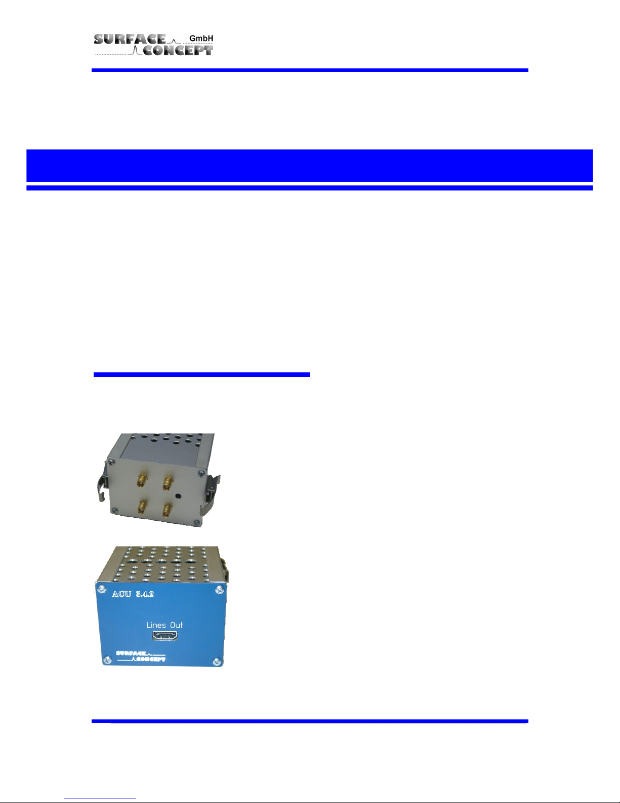
7.1 Pulse Processing Electronics ACU 3.4.2
The ACU 3.4.2 contains the pulse amplifiers, pulse shapers and constant fraction discriminators.
1. 4x SMB sockets for signal transfer from SMB feed-
through
2. Hole for orientation pin from SMB feed-through
3. 2 Clips for fastening the ACU to the detector flange
4. Connection socket for DLD readout cable
Figure 8: Layout of ACU 3.4.2
1
2
3
4
Page 25

DDeellaayylliinnee DDeetteeccttoorr DDLLDD 88008800
25
The ACU can be plugged directly onto the 4-fold SMB feed-throughs. Fasten the two clips of the ACU to fix it to
the detector. Figure 8 shows the layout of the ACU 3.4.2.
7.1.1 Positions of the Discriminator Threshold Regulators
Discriminator threshold regulators of the 4 DLD channels as well as potentiometers for an additional
adjustment can be found on the corresponding boards inside the ACU 3.4.2. They can be reached through
the holes on the top side of the ACU housing (see Figure 9).
The adjustment of the readout electronics goes hand in hand with the detector voltage. In fact there is only a
small “window” for an optimum setting of the readout electronics for a given operation voltage. Changes of
the detector voltage, other than to compensate loss in the amplification of the MCP stack due to wearing out
effects, will directly lead to a loss in performance of the readout electronics (artifacts within the image,
increased dark count rate etc.). The readout electronics is adjusted to its best performance to the operation
voltage of the detector when delivered. A new adjustment should not be needed. The operation voltage is
given in the specification sheet.
The sensitivity of the CFD is increased (threshold decreased) by turning the screw of the potentiometer
clockwise and vice versa for decreasing the sensitivity of the CFD. This is only to be used under some
circumstances where adjusting becomes necessary at all.
The readout electronics is adjusted to its best performance to the operation voltage of the
detector when delivered. Do not change the adjustment at all.
Changing the adjustment can easily end up with a status, where a readjustment must be
made by Surface Concept.
Figure 9: Labeling of discriminator threshold and amplification regulators.
X1 X2
Y1 Y2
A
mplification Regulator
Fraction Regulator
CFD Threshold
Zero Offset Regulator
Page 26

DDeellaayylliinnee DDeetteeccttoorr DDLLDD 88008800
26
8 Time-to-Digital-Converter (TDC)
8.1 Schematic Description of the USB2.0-TDC
The USB2.0-TDC serie combines the excellent performance of the GPX TDC chip (ACAM GmbH) with a field
programmable gate array (FPGA) and a high speed USB interface, either in the design with a single GPX chip
(USB2.0-TDC) or with two GPX chips (Double USB2.0-TDC) operated in I-mode with 82 ps bin size or with one
(Dual Channel USB2.0-TDC) or two GPX chips (Quad Channel USB2.0-TDC) operated in R-mode with 27 ps
time bin or G-mode with 36 ps time bin.
The FPGA enables comfortable setups and a variable data stream handling from the TDC via USB 2.0.
The main delayline detector and segment readout (optional device) functionality is permanently programmed.
A complex FIFO design makes data losses almost impossible. The user DLL controls the data handling and
streaming for the user. The Fourfold Quad Channel USB2.0-TDC combines in principle four units of the Quad
Channel USB2.0-TDCs in one device. It was especially developed for the readout of high rates of 4-Quadrant
Delayline Detectors.
In this light, the following brief description about the internal structure of the measurement unit is only
informative:
Figure 10: Schematic sketch of TDC functioning
Arrival times of pulses on the stop inputs are measured by the TDC with respect to either an internal
reference start signal, provided by the FPGA, or an external start signal. Data from the segments are read
out directly by the FPGA. The measurement dwell times for data from the TDC as well as from the segments
are settled within the FPGA by a quartz stabilized time gate in an interval from 1 ms to 1193 h. The
synchronization pulses for the external acquisition start (Sync. In) is fed directly into the FPGA, controlling the
Page 27

DDeellaayylliinnee DDeetteeccttoorr DDLLDD 88008800
27
acquisition process. The FPGA also sends out the synchronization pulse for marking the end of an acquisition
(Sync. Out). The TDC data streaming can be performed as measured (RawData mode) or including a DLD
specific data pre-conditioning (Pair mode). This concerns a channel pairing and a pair result arithmetic, a
modulo arithmetic and many more. Communication to and from the PC is achieved via a USB 2.0 interface.
Data streaming via the USB 2.0 interface is provided without losses using a large memory buffer within the
device.
8.2 Basic Operation Modes of the GPX TDC Chip
The GPX TDC chip can in principle be operated in the following modes. Not all modes are available for all USBTDC devices.
8.2.1 I-Mode (USB2.0-TDC/ Double USB2.0-TDC )
- 8 stop channels with typically 82.3 ps digital time bin resolution
- 1 start channel
- Input level: TTL or LVTTL
- 5.5 ns pulse-pair resolution on one channel and 0 ns between two channels
- 32-fold multi-hit capability = 182 MHz peak rate
- Trigger to rising or falling edge
- Measurement range: 0 ns – 10.6 µs in start-stop operation
(corresponds to a minimum start frequency of 94.4 kHz)
- Endless measurement range by internal retrigger of START
- 10 MHz continuous rate per channel
- 40 MHz continuous rate per chip
8.2.2 R-Mode (High Resolution/ Dual Channel/ Quad Channel USB2.0-TDC)
- 2 stop channels with typically 27.4 ps digital time bin resolution
- 1 start channel
- Input level: differential LVPECL
- 5.5 ns pulse-pair resolution on one channel and 0 ns between two channels
- 32-fold multi-hit capability = 182 MHz peak rate
- Trigger to rising or falling edge
- Measurement range: 0 ns – 40 µs in start-stop operation
(corresponds to a minimum start frequency of 25 kHz)
- Maximum Start Frequency: 7 MHz
- 40 MHz continuous rate per channel
- 40 MHz continuous rate per chip
8.2.3 G-Mode (High Resolution/ Dual Channel/ Quad Channel USB2.0-TDC)
- 2 stop channels with 41.2 ps digital time bin resolution
- 1 start channel
- Input level: differential LVPECL
- 5.5 ns pulse-pair resolution on one channel and 0 ns between two channels
- 32-fold multi-hit capability = 182 MHz peak rate
- Trigger to rising and
falling edge
- Measurement range: 0 ns - 65 µs
(corresponds to a minimum start frequency of 15.4 kHz)
- 40 MHz continuous rate per channel
- 40 MHz continuous rate per chip
Page 28

DDeellaayylliinnee DDeetteeccttoorr DDLLDD 88008800
28
8.3 Layout of the Quad Channel USB2.0-TDC
Figure 11: Layout of the Quad Channel USB2.0-TDC
1. TDC Power socket
2. BNC sockets for trigger
synchronization IN and OUT
3. HDMI socket for DLD readout cable
from ACU
4. USB 2.0 connection socket
5. BNC socket for TDC start input
6. Power switch to turn the TDC
ON/OFF. Lighted, when set to ON
8.3.1 TDC Inputs (Stop + Start)
The USB2.0-TDC provides a HDMI socket for the signal input (TDC INPUT) from the ACU. The TDC inputs are
laid out for PECL levels (R-mode operation mode).
An external start signal must be provided to the TDC for time resolved measurements. Apply standard TTL
signals to the “TTL START” input (BNC socket).
The USB2.0-TDC does not work with start signals of frequencies smaller than 25 kHz and
larger than 7 MHz. Therefore larger start pulse frequencies must be divided down with an
appropriate frequency divider (e.g. divider with factor of 16 for 80 MHz start pulse frequency).
The “modulo function” of the GUI software can be used to overlap multiple time spectra to
form one spectrum again.
The temporal resolution is influenced mainly by the quality of the start signal while the TDC measures the time
in a leading edge determination. Therefore, if the start signal is varying in time, one needs to process it by
means of a constant-fraction-discriminator or similar external electronics components.
8.3.2 Trigger Synchronization IN/OUT
Image acquisition of the DLD can be synchronized to an external trigger signal. To do so, the trigger signal
must be applied as TTL signal to the “SYNC IN” BNC socket of the USB2.0-TDC. The value of the variable
named “ext_gpx_start” in the dld_gpx3.ini file (see the manual of your end-user software, e.g. the GUI software
manual) must be set to “1”; otherwise the TDC ignores external trigger signals. The TDC provides a TTL signal
on the “SYNC OUT” BNC socket after each acquisition, independent on settings in the dld_gpx3.ini file.
1
2
3
6
4
5
Page 29

DDeellaayylliinnee DDeetteeccttoorr DDLLDD 88008800
29
8.3.3 Line Input
Electrical Input (LINE): 85 V – 260 V, 50/60 Hz
Power: 100 Watt (max.)
Fuse: 1x T 1.6 A
8.4 Interface (PC) and Software
All operation functions of the USB2.0-TDCs for data readout of the detector package are encapsulated in the
dynamic linked library “delayline.dll”. Data processing and presentation on the PC is realized by an end-user
software. See the corresponding software manuals for detailed information on the software package and the
DLL interface.
Page 30

DDeellaayylliinnee DDeetteeccttoorr DDLLDD 88008800
30
9 Dual HV Supply
This device produces lethal high voltage up to +5 kV. Hazardous voltages are present.
Therefore only persons with the appropriate training are allowed to carry out the
installation. Adjustment and repair work is only allowed to be carried out by SURFACE
CONCEPT.
The high voltage for the delayline detector is provided by an external high voltage power supply of the type
“Dual HV Supply”. It consists of the following:
• it holds 2 individual high voltage modules named HV A and HV B
• it provides 4 high voltage outputs (B+, B-, A & F) on SHV
• it provides 2 high voltage reference inputs (REF A, REF F) on SHV
• REF A is short cutted to A and REF F is short cutted to F, internally
• The operation voltage of the DLD is applied between A and F by HV A (the exact value for
the operation voltage is given within the specification sheet)
• The HV Filterbox must be connected between the Dual HV Supply and the DLD.
Do not operate the DLD without the HV filterbox.
• A and F must always be connected to the HV filterbox and from there to the DLD.
Do not connect any other HV output of the Dual HV Supply to the DLD !
• Depending on mode of operation (see details below), either REF F or REF A or B+ or B-
must be terminated to ground by using the termination plug.
• The output of the module HV B can be used to apply a positive (B+) or a negative (B-) bias
voltage to the DLD. To do so connect the corresponding output of HV B to either REF F or
REF A (depending on mode of operation, see details below).
The reference input of the MCP stack must either be terminated to ground or terminated with
a reference voltage from a second HV module. This must always be, because otherwise the
MCP stack is not functioning as the reference potential is missing.
• Ground the Dual HV Supply via the ground connector
• Finish the complete cabling, before the device is turned on
• Before the high voltage is switched on, make sure that the potentiometer (no. 3 & 6 in
Figure 12) are turned to the left as maximum possible (zero position of the HV modules) in
order to avoid high voltage sparks.
Page 31

DDeellaayylliinnee DDeetteeccttoorr DDLLDD 88008800
31
Increase the high voltage very carefully, especially when the detector is used for the first
time after installation or has been vented before. Strictly, follow the “Start-Up” procedure
described in chapter 10.2.
High voltage sparks may damage the meander or the MCPs seriously.
Do not disconnect the SHV cables, while high voltage is applied to the delayline detector.
This also will lead to high voltage sparks within the detector.
Do not open the power supply, while it is in operation. Hazardous voltages are present.
In case that the device must be opened, turn off the device first AND
pull out the power
plug.
9.1 Layout of Dual HV Supply & the HV filterbox
Dual HV Supply
1. High voltage turn ON/OFF for
HV module 1 (HV A)
2. Digital display for HV module A
3. Knob for high voltage adjustment
of HV module A
4. High voltage turn ON/OFF for
HV module 2 (HV B)
5. Digital display for HV module B
6. Knob for high voltage adjustment
of HV module B
7. Power switch, to turn ON/OFF
the power supply (lighted, when
set to ON)
8. Power socket
B+, B-, A, F : High voltage outputs via
SHV sockets
REF A, REF F: High voltage inputs for
reference voltages.
GND Ground connector
1
2
3
4
5
6
7
8
B+ A REF A
B
-
F REF F
GND
Page 32

DDeellaayylliinnee DDeetteeccttoorr DDLLDD 88008800
32
HV Filterbox
Figure 12: Layout of the Dual HV Supply & HV filterbox
A, F : High voltage inputs and
outputs via SHV sockets
9.1.1 Line Input of Dual HV Supply
Electrical Input (LINE): 230 V, 50 Hz
Power: 28 Watt (max.)
Fuse: 1x T 1.6 A
9.2 Connection schemes for different operation modes
The connection schemes for the different operation modes are given in the following figures. For the first
tests with the DLD we strongly recommend to apply the HV as illustrated in Figure 13.
Figure 13: Front side of MCP stack grounded, operation voltage between F & A. This is the
recommended operation mode to start off with.
from
HV Supply
To DLD
Page 33

DDeellaayylliinnee DDeetteeccttoorr DDLLDD 88008800
33
Figure 14: Detector anode grounded and operation voltage between F & A.
Figure 15: Positive bias voltage applied to the front side of the MCP stack. The operation voltage
between F & A is unchanged.
Page 34

DDeellaayylliinnee DDeetteeccttoorr DDLLDD 88008800
34
Figure 16: Negative bias voltage applied to the front side of the MCP stack. The operation voltage
between F & A is unchanged.
Figure 17: Positive bias voltage applied to the detector anode. The operation voltage between F & A is
unchanged.
Page 35

DDeellaayylliinnee DDeetteeccttoorr DDLLDD 88008800
35
Figure 18: Negative bias voltage applied to the detector anode. The operation voltage between F & A is
unchanged.
Page 36

DDeellaayylliinnee DDeetteeccttoorr DDLLDD 88008800
36
10 Operation of the DLD
10.1 Getting Started
• Be sure, that the vacuum pressure at the detector is remarkably below 10
-6
mbar, otherwise the
microchannel plates might be damaged by a local discharging (in general: the lower the pressure,
the longer the lifetime of the MCPs).
• Finish the complete cabling as described in chapter 3 and turn on the TDC.
• Use the high voltage connection as shown in Figure 13, for the first tests of the DLD.
• Start the GUI software and within it the Rate Meter. For details see the GUI software manual.
• Turn off all sources for electrons, ions, light or X-rays that might hit the detector.
The ion-gauge and the gatterpump are both sources for electrons, ions and also X-rays
(the gatterpump). They can produce so many particles/ X-rays, that the detector is in a
complete overload, even when they are not facing the detector directly. This will wear out
the MCPs very fast. Turn off gatterpump and ion-gauge, if they are too close and/or in
direct direction to the detector.
• Turn on the high voltage carefully, as described in the following chapter.
10.2 Turning on the High Voltage
High voltage sparks may seriously damage the meander or the MCPs. Observe the
chamber pressure carefully every time the high voltage is turned on. Switch off the high
voltage immediately in case of a temporary pressure rise by an order of magnitude or
more. This indicates high voltage sparking.
If sparking occurs, turn down the high voltage immediately and wait some time (up to 5
min.). Start the “Start-Up” procedure again with an increased ramp time. Is it not be
possible to reach the operation voltage without sparking, then turn off the high voltage,
stop the procedure and call SURFACE CONCEPT for further assistance.
Page 37

DDeellaayylliinnee DDeetteeccttoorr DDLLDD 88008800
37
10.2.1 “Start-Up” Procedure (for new systems and for systems, after being vented)
The first time the detector is used or after the system has been vented, the detector high voltages must be
ramped very slowly to the final operation value. The voltage increase should not exceed 100 V per minute.
A schematic sketch on how to ramp the voltages during the “Start-Up” procedure is given in Figure 19.
Figure 19: Schematic sketch on voltage ramping during “Start-Up” procedure.
• First start to ramp the operation voltage of the DLD (output: HV A) to the specified operation
voltage (see specification sheet for exact values).
• The ramping of an additional bias (reference) voltage (e.g. output of HV B) should only be
made after the ramping of the operation voltage has been finished (t3 > t2).
• The bias voltage (connected to REF F or REF A) should not exceed a value of more than ±
1700 V.
The analogue readout electronics has been adjusted to an optimized detector voltage.
This specified voltage is given in the specification sheet of the detector. There you also
find a maximum operation voltage. Never exceed this voltage.
Stick to the voltages given in the specification sheet. Contact Surface Concept before
any other – especially higher – voltages are applied to the detector.
Do not forget to connect the termination plug (see Figure 13 - Figure 18 for details).
Example:
A detector with an exemplary operation voltage of +2500 V should be operated with an exemplary
bias voltage of +500 V. Therefore a ramp time of 25 min. should be used to change the operation voltage
from GND or 0 V on ref. potential to +2500 V using HV module “HV A”. After this the bias voltage is ramped
to +500 V in a ramp time of 5 min using for example the HV module “HV B”.
Page 38

DDeellaayylliinnee DDeetteeccttoorr DDLLDD 88008800
38
• After high voltage has been applied to the detector, check the detector output by means of the
GUI software. The dark count rate without any source should correspond to the value given in
the specification sheet.
• Now you may start carefully with an electron/ light source observing the detector output.
Keep in mind the description about the important operation details in chapter 5.4.
10.2.2 Standard Start Procedure
The following procedure is used for all later starts, when the detector has already been operated in vacuum
and has not been vented in between:
• Turn off all sources for electrons, ions, light or X-rays that might hit the detector.
The ion-gauge and the gatterpump are both sources for electrons, ions and also X-rays
(the gatterpump). They can produce so many particles/ X-rays, that the detector is in a
complete overload, even when they are not facing the detector directly. This will wear out
the MCPs very fast. Turn off gatterpump and ion-gauge, if they are too close and/or in
direct direction to the detector.
• Turn up the high voltage carefully and stepwise within 2 or 3 minutes to the operation voltage.
• Ramp the operation voltage before any additional bias voltage.
• Watch the vacuum pressure during this procedure; turn the voltages back, if an unusual
increase is observed in the pressure.
• After high voltage has been applied to the detector, check the detector output by means of the
GUI software. The dark count rate without any source should correspond to the value given in
the specification sheet.
• Now you may start carefully with an electron source observing the detector output.
Keep in mind the description about the important operation details in chapter 5.4.
Turn off the high voltage, close the software and turn off the TDC before performing any
changes of the cabling.
Page 39

DDeellaayylliinnee DDeetteeccttoorr DDLLDD 88008800
39
10.3 Bake Out Procedure
The maximum allowed temperature for the detector is 150°C. Do not exceed this
temperature.
• Please read the bake out instruction completely and carefully, before starting the bake out
procedure.
• Windows and feed-throughs should be wrapped with aluminum foil, to protect them from rapid
temperature changes.
• The use of heating tapes and jackets is not recommended, due to danger of local overheating.
• Do not remove the blankets until the entire system has thoroughly cooled off.
• Do not operate the detector before the temperature has returned to ambient conditions.
• The detector electronics (ACU) must be removed before any bake out.
After a bake out, the detector needs at least half a day (approx. 12 hours) to cool down. If
channel plates are operated at higher temperatures (> 50°C) they can suffer damage.
Such channel plates will lose gain and exhibit a markedly higher detector plateau.
Even if the detector housing feels just warm, any internal parts seated on insulators (e.g.
the meander detector) may still be too hot for safe operation. It is imperative that all
users be informed of this issue and take the necessary precaution to ensure proper
device operation.
Page 40

DDeellaayylliinnee DDeetteeccttoorr DDLLDD 88008800
40
11 Microchannel Plate (MCP)
Contact SURFACE CONCEPT before performing a replacement.
Take care to note the orientation of the MCPs. The channels in the MCPs include a certain angle against the
surface normal to the plate and the MCPs must be mounted in a chevron or z-stack configuration (depending
on no. of MCPs). All parts of the detector, especially the MCPs should be handled with great care. The MCP
surfaces are very sensitive and should never be touched or scratched.
11.1 Storage
Because of their structure and the nature of the materials used in manufacture, care must be taken when
handling or operating MCPs. The following precautions are strongly recommended:
• The most effective long-term storage environment for an MCP is an oil-free vacuum.
11.2 Handling
• Shipping containers should be opened only under class 100 Laminar flow cleanroom conditions.
• Personnel should always wear clean, talc-free, class 100 clean-room compatible, vinyl gloves when
handling MCPs. No physical object should come into contact with the active area of the wafer. The
MCP should be handled by its rims, there is no solid glass border! Use clean degassed tools
fabricated from stainless steel, Teflon™ or other ultra-high vacuum-compatible materials. Handling
MCPs should be limited to trained, experienced personnel.
• MCPs without solid glass border should be handled very carefully with great care taken to contact
the outer edges of the plate only.
• The MCP should be protected from exposure to particle contamination. Particles which become
affixed to the plate can be removed by using a very pure and low pressure air flow such as from a
clean rubber bellows.
• The MCP should be mounted only in fixtures designed for this purpose. Careful note should be
taken of electrical potentials involved.
Page 41

DDeellaayylliinnee DDeetteeccttoorr DDLLDD 88008800
41
Voltages must not be applied to the device while at atmospheric pressure. The pressure
should be 1 x 10
-6
mbar or lower at the microchannel plate before applying voltage.
Otherwise, damaging ion feedback or electrical breakdown will occur.
11.3 Operation
• A dry-pumped or well-trapped/diffusion-pumped operating environment is desirable. A poor
vacuum environment will most likely shorten MCP life or change MCP operating characteristics.
• A pressure of 1 x 10
-6
mbar or better is preferred. Higher pressure can result in high background
noise due to ion feedback.
• When a satisfactory vacuum has been achieved, voltages may be applied. It is recommended that
this is done slowly and carefully. If fluctuations do appear, damage or contamination should be
suspected and the voltage should be turned off. The assembly should then be inspected before
proceeding.
• Voltage across single MCPs should not exceed the max. voltage given in Table 2 and in the
specification sheet of the detector. Higher potentials may result in irreversible damage.
• MCPs can be degraded by exposure to various types of hydrocarbon materials which raise the
work function of the surface, causing gain degradation.
• Operation at higher temperatures (> 50 °C) will cause gain degradation.
Thickness 1.5 mm
Outer diameter 86,6 mm
Active diameter 80 mm
L/D (channel length / channel diameter) 60 : 1
Resistance (single MCP) 1.6 – 6 MOhms
Max. voltage (single MCP) 1200 V
Max. Gain @ 1200 V
≥ 1 ⋅ 10
5
minimum
Pore size (diameter) 25 µm
Center – to – Center Spacing 32 µm
Bias angle of channels 19° ± 1°
Quality level detection quality, extended dynamic range
Open area ratio 45 % minimum
Operating pressure
< 1 ⋅ 10
-6
mbar
Table 2: MCP Specifications
Page 42

DDeellaayylliinnee DDeetteeccttoorr DDLLDD 88008800
42
12 Technical Data
Delayline detector General:
HV capability: none
Active area: ∅ 80 mm round
Operation voltage at detector: see specification sheet
Max. voltage at DLD: see specification sheet
Max. bias voltage: +/- 1700 V (depending on cabling)
Max. bake-out temperature: 150°C
Vacuum pressure range for operation: < 10
-6
mbar
Amplifier – CFD – Unit ACU 3.16.2:
No. of Amplifier-CFD channels: 4
Bandwidth of DLD amplifiers: 1.6 GHz
CFD working frequency: 200 MHz
CFD jitter (max.): 20ps
CFD walk (typ.): < 50 ps (while ambient temperature varies less then 5 K)
Page 43

DDeellaayylliinnee DDeetteeccttoorr DDLLDD 88008800
43
13 List of Figure
Figure 1: Contents of delivery package .............................................................................................................................................. 10
Figure 2: 0/0 position of the DLD image (black dot)................................................................................................................... 12
Figure 3: Connection scheme of the delayline detector and readout package................................................................ 12
Figure 4: Principle of the 3D (x, y, t) delayline operation............................................................................................................. 18
Figure 5: Schematic orientation and naming of the two meander structured delaylines........................................... 21
Figure 6: Connection ports for the DLD8080................................................................................................................................ 22
Figure 7: Internal connection of high voltage potentials (schematic)................................................................................... 22
Figure 8: Layout of ACU 3.4.2................................................................................................................................................................ 24
Figure 9: Labeling of discriminator threshold and amplification regulators...................................................................... 25
Figure 10: Schematic sketch of TDC functioning.......................................................................................................................... 26
Figure 11: Layout of the Quad Channel USB2.0-TDC.................................................................................................................. 28
Figure 12: Layout of the Dual HV Supply & HV filterbox............................................................................................................. 32
Figure 13: Front side of MCP stack grounded, operation voltage between F & A. This is the recommended
operation mode to start off with. ................................................................................................................................................32
Figure 14: Detector anode grounded and operation voltage between F & A................................................................... 33
Figure 15: Positive bias voltage applied to the front side of the MCP stack. The operation voltage between F &
A is unchanged....................................................................................................................................................................................33
Figure 16: Negative bias voltage applied to the front side of the MCP stack. The operation voltage between F
& A is unchanged............................................................................................................................................................................... 34
Figure 17: Positive bias voltage applied to the detector anode. The operation voltage between F & A is
unchanged............................................................................................................................................................................................. 34
Figure 18: Negative bias voltage applied to the detector anode. The operation voltage between F & A is
unchanged............................................................................................................................................................................................. 35
Figure 19: Schematic sketch on voltage ramping during “Start-Up” procedure............................................................. 37
Page 44

DDeellaayylliinnee DDeetteeccttoorr DDLLDD 88008800
44
EU Declaration of Conformity
Manufacturer Surface Concept GmbH
Staudinger Weg 7
D - 55128 Mainz
Germany
Product details Delayline Detector DLD 1D, 2D, 3D, Quadrant in all variations
and sizes to be operated with ACU and USB2.0-TDC in all
versions and subversions.
The above named products comply with the following European directive:
89/336/EEC Electromagnetic Compatibility Directive, amended by 91/263/ EEC
and 92/31/ EEC and 93/68/EEC
73/23/EEC Low Voltage Equipment Directive, amended by 93/68/EEC
The compliance of the above named product to which this declaration relates are in
conformity with the following standards or other normative documents where
relevant:
EN 50081-1 (3/94) Electromagnetic Compatibility Generic Emission Standard-Part 1:
EN50082-1 (3/94) Electromagnetic Compatibility
EN 61010-1 (2001) Safety Requirements for Electrical Equipment for Measurement,
Control and Laboratory Use
Issued on 01. February 2008
For and on behalf of Surface Concept GmbH
This declaration does not represent a commitment to features or capabilities of the instrument. The
safety notes and regulations given in the product related documentation must be observed at all times.
Page 45

DDeellaayylliinnee DDeetteeccttoorr DDLLDD 88008800
45
EU Declaration of Conformity
Manufacturer Surface Concept GmbH
Staudinger Weg 7
D - 55128 Mainz
Germany
Product details High voltage power supplies “Single HV Supply” and “Dual HV
Supply”
The above named products comply with the following European directive:
89/336/EEC Electromagnetic Compatibility Directive, amended by 91/263/ EEC
and 92/31/ EEC and 93/68/EEC
73/23/EEC Low Voltage Equipment Directive, amended by 93/68/EEC
The compliance of the above named product to which this declaration relates are in
conformity with the following standards or other normative documents where
relevant:
EN 50081-1 (3/94) Electromagnetic Compatibility Generic Emission Standard-Part 1:
EN50082-1 (3/94) Electromagnetic Compatibility
EN 61010-1 (2001) Safety Requirements for Electrical Equipment for Measurement,
Control and Laboratory Use
Issued on 01. February 2008
For and on behalf of Surface Concept GmbH
This declaration does not represent a commitment to features or capabilities of the instrument. The
safety notes and regulations given in the product related documentation must be observed at all times.
 Loading...