

Page 1
Supertex inc.
Adjustable 3-Terminal Linear Regulator
LR8
High Input Voltage,
Features
► 13.2 - 450V input voltage range
► Adjustable 1.20 - 440V output regulation
► 5% output voltage tolerance
► Output current limiting
► 10µA typical ADJ current
► Internal junction temperature limiting
Applications
► Off-line SMPS startup circuits
► Adjustable high voltage constant current source
► Industrial controls
► Motor controls
► Battery chargers
► Power supplies
General Description
The Supertex LR8 is a high voltage, low output current, adjustable
linear regulator. It has a wide operating input voltage range of
13.2 - 450V. The output voltage can be adjusted from 1.20 - 440V
provided that the input voltage is at least 12V greater than the
output voltage. The output voltage can be adjusted by means of
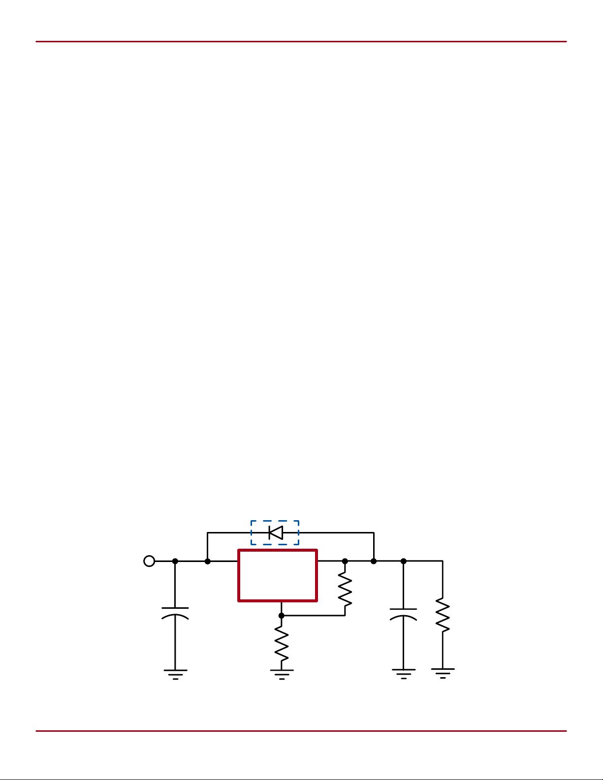
two external resistors R1 and R2 as shown in the typical application
circuits. The LR8 regulates the voltage difference between VOUT
and ADJ pins to a nominal value of 1.20V. The 1.20V is amplied
by the external resistor ratio R1 and R2. An internal constant
bias current of typically 10µA is connected to the ADJ pin. This
increases V
The LR8 has current limiting and temperature limiting. The output
current limit is typically 20mA and the minimum temperature limit
is 125°C. An output short circuit current will therefore be limited
to 20mA. When the junction temperature reaches its temperature
limit, the output current and/or output voltage will decrease to
keep the junction temperature from exceeding its temperature
limit. For SMPS start-up circuit applications, the LR8 turns off
when an external voltage greater than the output voltage of the
LR8 is applied to VOUT of the LR8. To maintain stability, a bypass
capacitor of 1.0µF or larger and a minimum DC output current of
500µA are required.
by a constant voltage of 10µA times R2.
OUT
Typical Application Circuit
V
IN
C
1
* Required for conditions where VIN is less than V
VIN
LR8
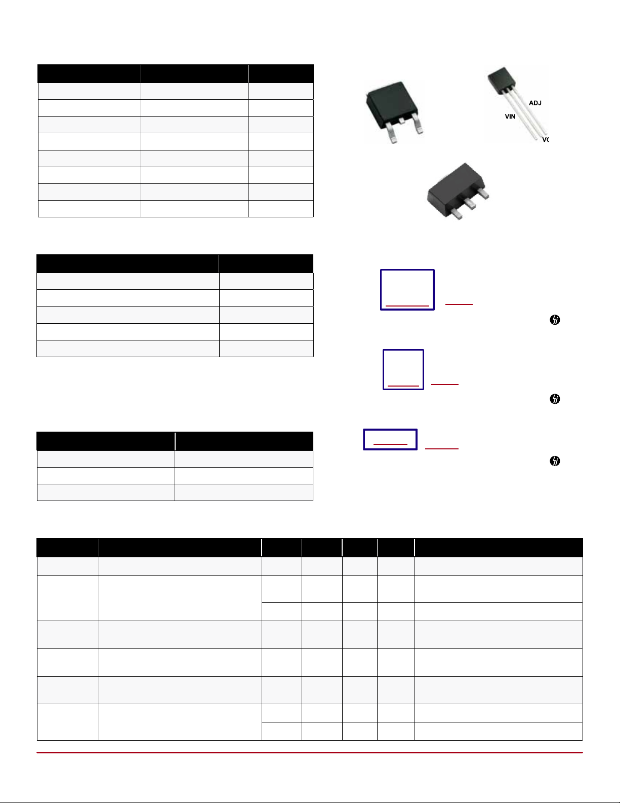
The device is available in TO-243AA (SOT-89), TO-252 (D-PAK),
and TO-92 packages.
*
V
OUT
VOUT
ADJ
R
2
R
1
C
OUT
2
R
LOAD
.
Doc.# DSFP-LR8
B080113
Supertex inc.
www.supertex.com
Page 2
LR8
VOUT
VOUT
Ordering Information
Part Number Package Options Packing
LR8K4-G TO-252 (D-PAK) 2000/Reel
LR8N3-G TO-92 1000/Bag
LR8N3-G P002 TO-92 2000/Reel
LR8N3-G P003 TO-92 2000/Reel
LR8N3-G P005 TO-92 2000/Reel
LR8N3-G P013 TO-92 2000/Reel
LR8N3-G P014 TO-92 2000/Reel
LR8N8-G TO-243AA (SOT-89) 2000/Reel
-G denotes a lead (Pb)-free / RoHS compliant package
Absolute Maximum Ratings
Parameter Value
VIN input voltage (voltages ref to ADJ) -0.5V to +480V
Output voltage range -0.5V to +470V
Operating ambient temperature range -40°C to +85°C
Operating junction temperature range -40°C to +125°C
Storage temperature range -65°C to +150°C
Stresses beyond those listed under “Absolute Maximum Ratings” may cause permanent
damage to the device. These are stress ratings only, and functional operation of the
device at these or any other conditions beyond those indicated in the operational sections
of the specications is not implied. Exposure to absolute maximum rating conditions for
extended periods may affect device reliability.
Typical Thermal Resistance
Package θ
TO-252 (D-PAK) 81OC/W
TO-92 132OC/W
TO-243AA (SOT-89) 133OC/W
ja
Pin Conguration
ADJ
VIN
ADJ
TO-92TO-252 (D-PAK)
VOUT
ADJ
VOUT
VIN
TO-243AA (SOT-89)
Product Marking
Si YYWW
LR8K4
LLLLLLL
Package may or may not include the following marks: Si or
SiLR
8
YWLL
Package may or may not include the following marks: Si or
LR8W
Package may or may not include the following marks: Si or
TO-243AA (SOT-89)
YY = Year Sealed
WW = Week Sealed
L = Lot Number
= “Green” Packaging
TO-252 (D-PAK)
Y = Last Digit of Year Sealed
W = Code for Week Sealed
L = Lot Number
= “Green” Packaging
TO-92
W = Code for Week Sealed
= “Green” Packaging
Electrical Characteristics
(Test conditions unless otherwise specied: -40°C < TA < 85°C.)
Sym Parameter Min Typ Max Units Conditions
VIN - V
V
OUT
ΔV
OUT
ΔV
OUT
ΔV
OUT
I
OUT
Doc.# DSFP-LR8
B080113
Input to output voltage difference 12 - 450 V ---
OUT
1.14 1.20 1.26 V
Overall output voltage regulation
375 400 425 V R
Line regulation - 0.003 0.01 %/V
Load regulation - 1.4 3.0 %
Temperature regulation -1 - +1 %
10 - 30 mA TJ < 85°C, VIN - V
Output current limit
- - 0.5 mA TJ > 125°C, VIN - V
2
13.2V < VIN< 400V,
R1 = 2.4kΩ, R2 = 0
17V < VIN< 400V, V
I
OUT
VIN = 17V, V
0.5mA <I
VIN = 17V, V
-40°C < TA < 85°C
= 2.4kΩ, R2 = 782kΩ
1
OUT
= 0.5mA
= 5V,
OUT
< 10mA
OUT
= 5V, I
OUT
= 12V
OUT
OUT
Supertex inc.
www.supertex.com
= 5V,
= 10mA,
OUT
= 450V
Page 3
Electrical Characteristics (cont.)
(Test conditions unless otherwise specied: -40°C < TA < 85°C.)
Sym Parameter Min Typ Max Units Conditions
I
Minimum output current - 0.3 0.5 mA Includes R1 and load current
OUT
I
ADJ
Adjust output current 5.0 10 15 µA ---
C2 Minimum output load capacitance 1.0 - - µF ---
DV
/DVIN Ripple rejection ratio 50 60 - dB 120Hz, V
OUT
T
LIMIT
Junction temperature limit 125 - - °C ---
Thermal Characteristics
OUT
LR8
= 5V
Package
Power Dissipation
@ TA = 25°C
θ
jc
°C/W
°C/W
TO-92 0.74W 125 170
TO-243AA 1.6W 15 78
TO-252 2.5W 6.25 50
Note:
† Mounted on FR4 board, 25mm x 25mm x 1.57mm.
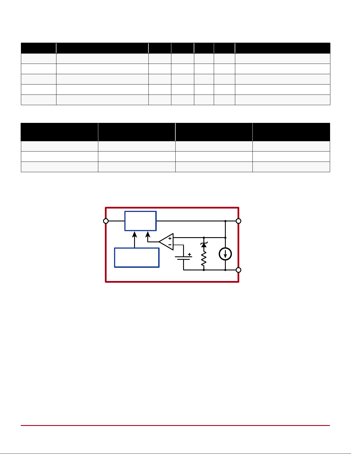
Functional Block Diagram
VIN
Pass
Element
Overtemp &
Overcurrent
10µA 1.2V
VOUT
ADJ
LR8
θ
ja
†
†
Doc.# DSFP-LR8
B080113
Supertex inc.
3
www.supertex.com
Page 4
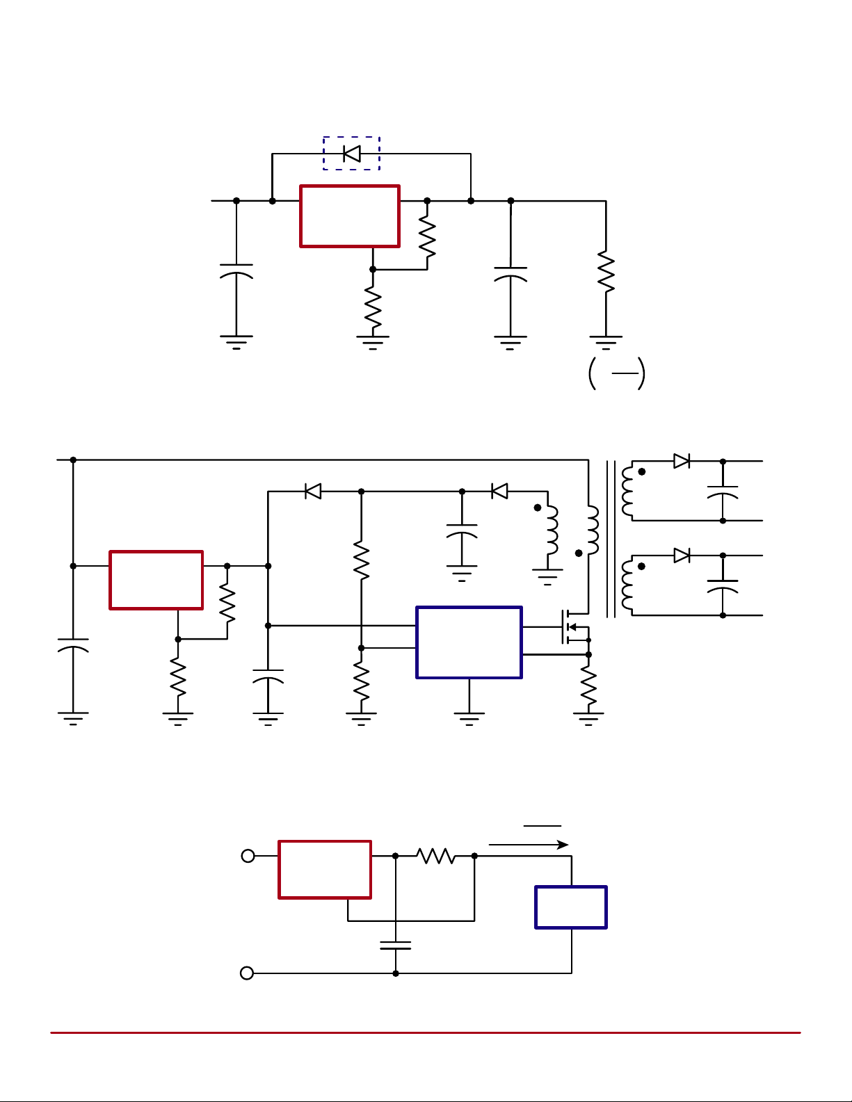
Typical Application Circuits
*
Figure 1: High Input Voltage, 5.0V Output Linear Regulator
V
=
IN
17 to 450V
C
1
* Required for conditions where V
Figure 2: SMPS Start-Up Circuit
VIN
LR8
VOUT
ADJ
R
2
18.2kΩ
1%
is less than V
IN
R
1
6.04kΩ
1%
OUT
V
= 5.0V
OUT
C
2
1.0µF
V
= 1.20V 1+
OUT
R
R
R
LOAD
2
1
≤16.5kΩ
+ I
ADJ
LR8
V
IN
= (V
+ 12V) to 450V
OUT
VIN
LR8
VOUT
ADJ
V
AUXILIARY
V
CC
FB
PWM IC
Figure 3: High Voltage Adjustable Constant Current Source
I
+
VIN
VOUT
R
OUT
=
1.20V
R
+
1
V
OUT
-
+
V
1
OUT
-
Doc.# DSFP-LR8
B080113
V
=
IN
(V
+ 12V) to 450V
OUT
-
LR8
ADJ
1.0µF
4
Load
Supertex inc.
www.supertex.com
Page 5
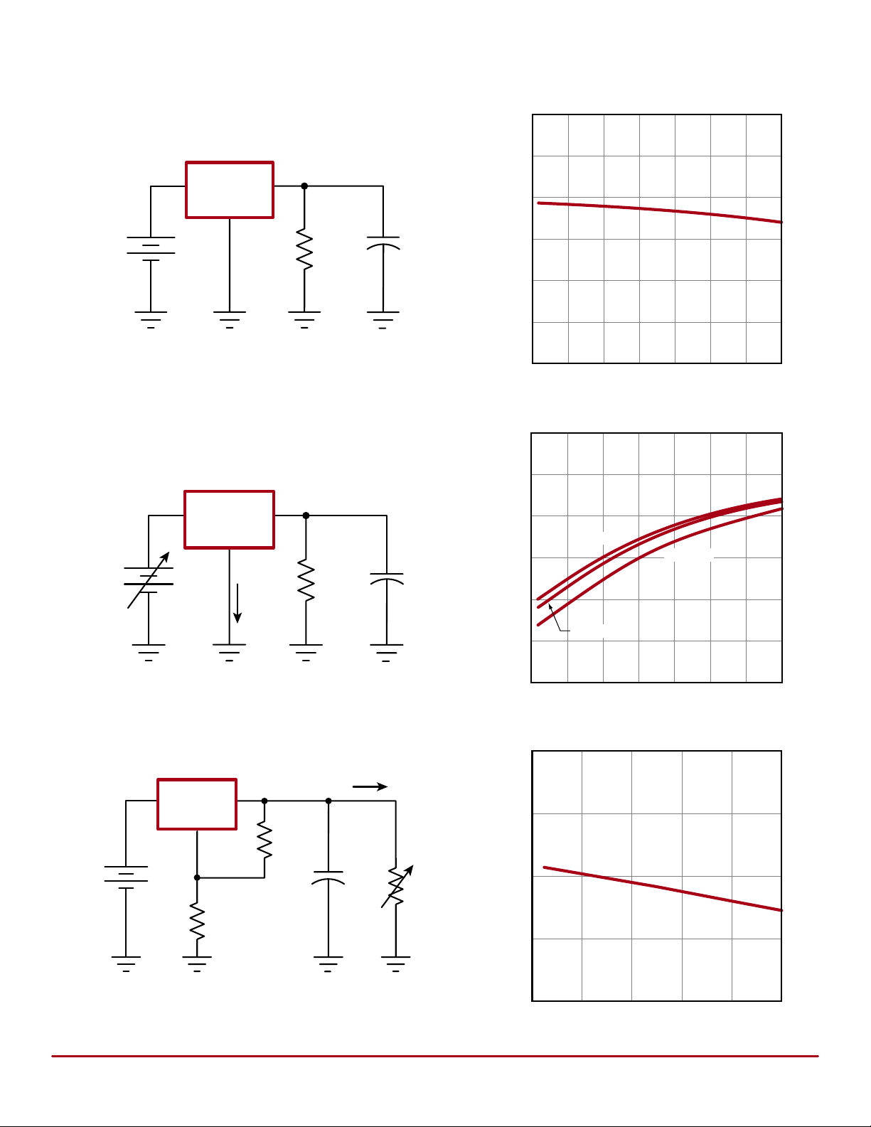
Typical Performance Curves
V
IN
LR8
V
OUT
LR8
Temperature Variation
1.30
1.25
= 1.2V
1.20
12V
12V,
200V
400V
ADJ
2.4k
Ω
1.0µF
(V)
1.15
OUT
V
1.10
1.05
1.00
-50 -25 0 25 50 75 100 125
T (junction) (OC)
Adjustment Current
12
11
I
ADJ
V
OUT = 1.2V
2.4kΩ
1.0ΩF
10
(µA)
ADJ
I
V
= 400V
IN
9
8
V
= 200V
7
IN
V
IN
= 12V
V
IN
LR8
ADJ
25V
Doc.# DSFP-LR8
B080113
6
-50 -25 0 25 50 75 100 125
T (junction) (OC)
Load Regulation
5.2
V
V
IN
LR8
ADJ
OUT
= 5.0V
6.04kΩ
±
1%
I
OUT
1.0µF
R
LOAD
(V)
V
OUT
5.1
5.0
18.2kΩ
±
1%
4.9
4.8
0 2 4 6 8 10
I
(mA)
OUT
Supertex inc.
5
www.supertex.com
Page 6
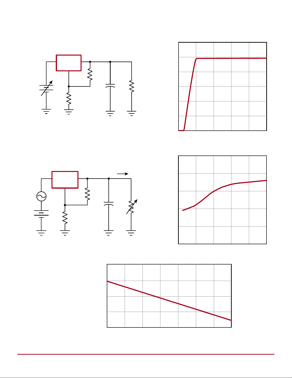
Typical Performance Curves (cont.)
05
V
V
IN
LR8
OUT
= 5.0V
LR8
V
vs. V
6
OUT
5
IN
0V to 50V
20V
P-P
@ 60Hz
65V
ADJ
18.2kΩ
±1%
6.04kΩ
±1%
1.0µF
1kΩ
4
(V)
3
OUT
V
2
1
0
01020304
V
(V)
IN
0
Ripple Rejection
-65
V
IN
V
= 5.0V
OUT
I
OUT
-64
LR8
ADJ
18.2kΩ
±
1%
6.04kΩ
±
1%
1.0µF
R
LOAD
-63
-62
Ripple Regection Ratio (dB)
-61
Doc.# DSFP-LR8
B080113
-60
0 2 4 6 8 10
I
30
25
20
(mA)
CL
l
15
10
-40 -20 0 20 40 60 80 100
Temperature (OC)
6
(mA)
OUT
Supertex inc.
www.supertex.com
Page 7
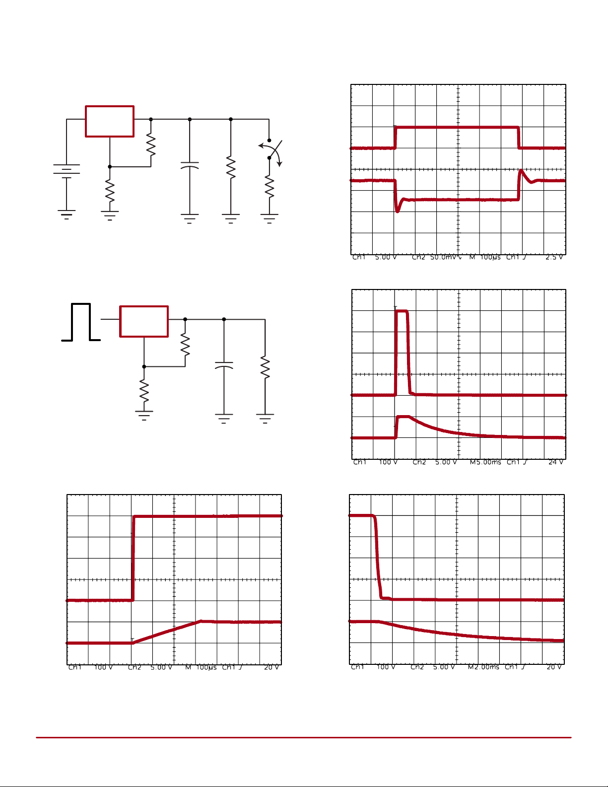
Typical Performance Curves (cont.)
Load Transient Response
V
OUT
= 5.0V
6.04kΩ
±1%
1.0µF
10kΩ
25V
V
IN
LR8
ADJ
18.2kΩ
±1%
Line Transient Response
sw
532Ω
Closed
SW
Open
V
OUT
LR8
Load Transient Response
400V
V
IN
0V
400V
V
V
IN
OUT
= 5.0V
400V
LR8
ADJ
18.2kΩ
±1%
V
IN
6.04kΩ
±1%
1.0µF
10kΩ
V
400V
V
V
0V
OUT
0V
IN
Line Transient Response
IN
0V
5.0V
V
OUT
0V
Doc.# DSFP-LR8
B080113
Line Power Up Transient
0V
5.0V
V
OUT
0V
Line Power Down Transient
Supertex inc.
7
www.supertex.com
Page 8
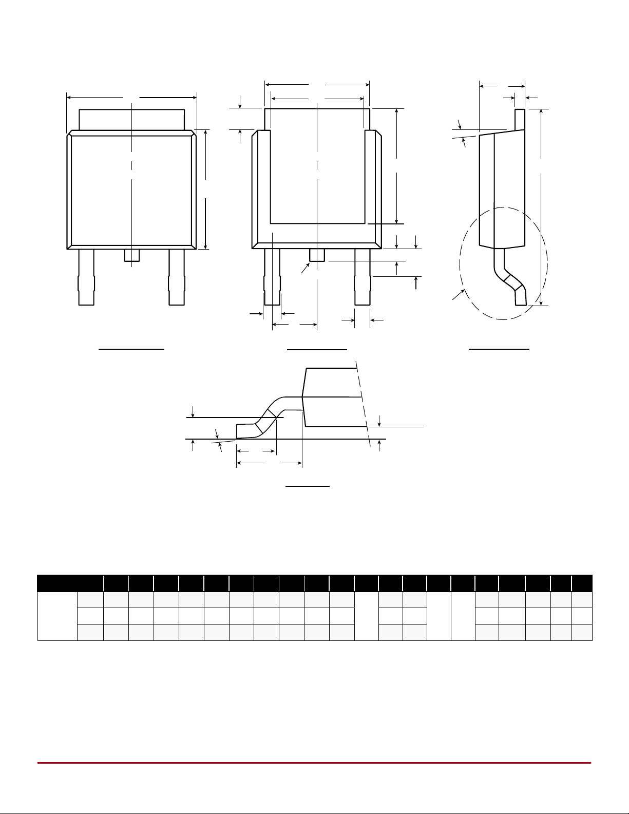
3-Lead TO-252 D-PAK Package Outline (K4)
LR8
E
4
1 2 3
Front View
b3
E1
L3
θ1
D1
D
L4
L5
Note 1
b2
e
Rear View
b
View B
Side View
A
c2
H
L2
Gauge
Plane
θ
L
L1
A1
Seating
Plane
View B
Note:
1. Although 4 terminal locations are shown, only 3 are functional. Lead number 2 was removed.
Symbol A A1 b b2 b3 c2 D D1 E E1 e H L L1 L2 L3 L4 L5
Dimen-
sion
(inches)
JEDEC Registration TO-252, Variation AA, Issue E, June 2004.
* This dimension is not specied in the JEDEC drawing.
†
This dimension differs from the JEDEC drawing.
Drawings not to scale.
Supertex Doc. #: DSPD-3TO252K4, Version F040910.
MIN .086 .000* .025 .030 .195 .018 .235 .205 .250 .170
NOM - - - - - - .240 - - - - .060 - - - - -
MAX .094 .005 .035 .045 .215 .035 .245 .217* .265 .200* .410 .070 .050 .040 .060 10O15
.090
BSC
.370 .055
.108
REF
.035 .025* .035†0O0
.020
BSC
θ
θ1
O
O
Doc.# DSFP-LR8
B080113
Supertex inc.
8
www.supertex.com
Page 9
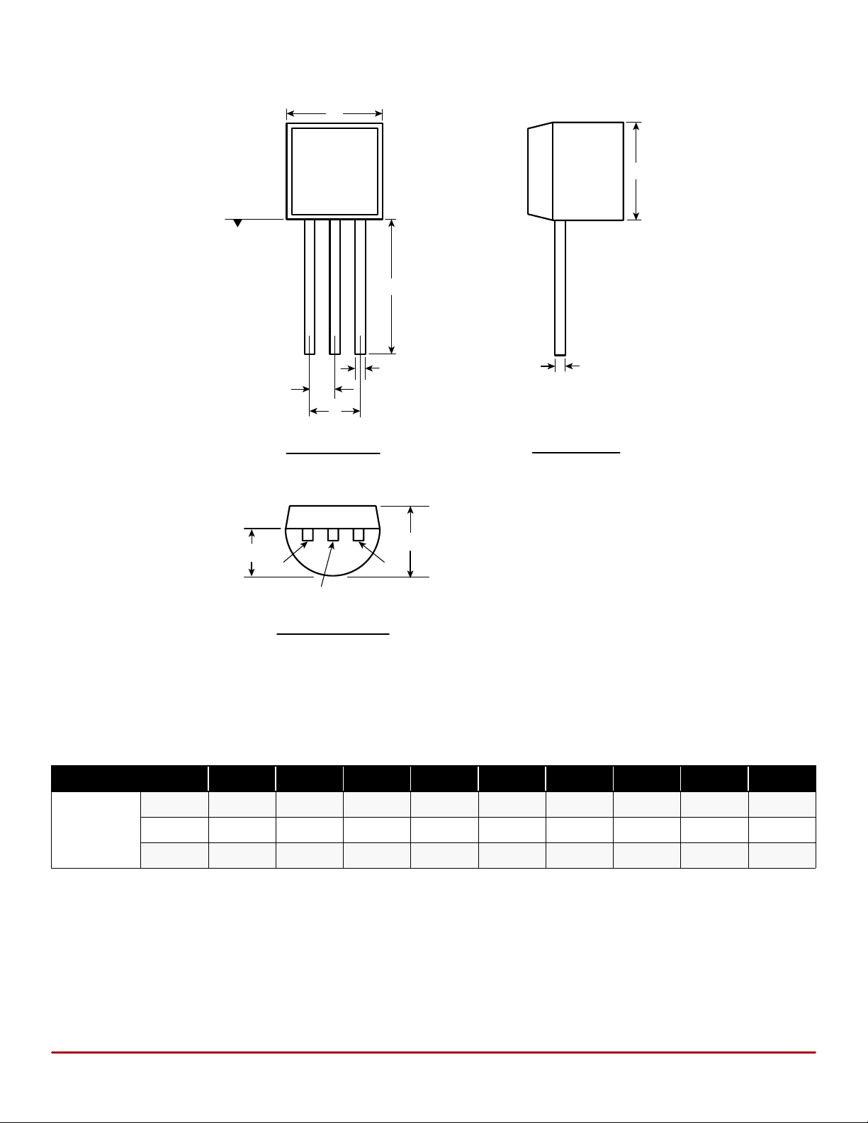
3-Lead TO-92 Package Outline (N3)
D
Seating
Plane
1 2 3
L
LR8
A
Front View
E1
1
Bottom View
e1
b
e
c
Side View
E
3
2
Symbol A b c D E E1 e e1 L
MIN .170 .014
Dimensions
(inches)
NOM - - - - - - - - -
MAX .210 .022
JEDEC Registration TO-92.
* This dimension is not specied in the JEDEC drawing.
† This dimension differs from the JEDEC drawing.
Drawings not to scale.
Supertex Doc.#: DSPD-3TO92N3, Version E041009.
Doc.# DSFP-LR8
B080113
†
†
.014
.022
†
.175 .125 .080 .095 .045 .500
†
.205 .165 .105 .105 .055 .610*
Supertex inc.
9
www.supertex.com
Page 10
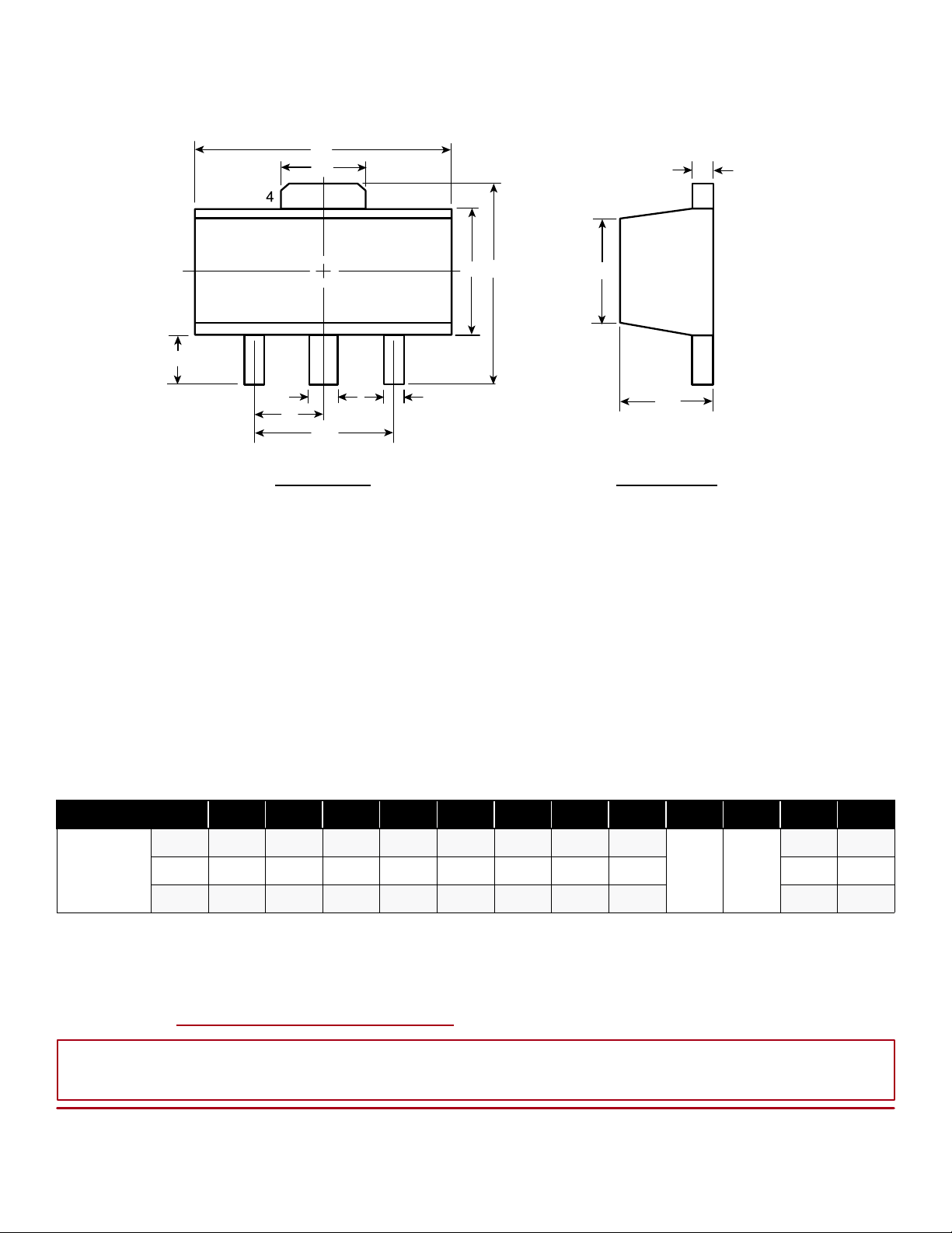
3-Lead TO-243AA (SOT-89) Package Outline (N8)
D
D1
E
H
E1
C
LR8
L
1 2 3
b
e
e1
Top View
b1
A
Side View
Symbol A b b1 C D D1 E E1 e e1 H L
†
1.50
BSC
3.00
BSC
3.94 0.73
Dimensions
(mm)
MIN 1.40 0.44 0.36 0.35 4.40 1.62 2.29 2.00
NOM - - - - - - - - - -
MAX 1.60 0.56 0.48 0.44 4.60 1.83 2.60 2.29 4.25 1.20
JEDEC Registration TO-243, Variation AA, Issue C, July 1986.
† This dimension differs from the JEDEC drawing
Drawings not to scale.
Supertex Doc. #: DSPD-3TO243AAN8, Version F111010.
(The package drawing(s) in this data sheet may not reect the most current specications. For the latest package outline
information go to http://www.supertex.com/packaging.html.)
Supertex inc. does not recommend the use of its products in life support applications, and will not knowingly sell them for use in such applications unless it receives
an adequate “product liability indemnification insurance agreement.” Supertex inc. does not assume responsibility for use of devices described, and limits its liability
to the replacement of the devices determined defective due to workmanship. No responsibility is assumed for possible omissions and inaccuracies. Circuitry and
specifications are subject to change without notice. For the latest product specifications refer to the Supertex inc. (website: http//www.supertex.com)
©2013 Supertex inc. All rights reserved. Unauthorized use or reproduction is prohibited.
Doc.# DSFP-LR8
B080113
10
Supertex inc.
1235 Bordeaux Drive, Sunnyvale, CA 94089
Tel: 408-222-8888
www.supertex.com
†
 Loading...