

Page 1
Supertex inc.
Supertex inc. ● 1235 Bordeaux Drive, Sunnyvale, CA 94089 ● Tel: 408-222-8888 ● www.supertex.com
LED Driver with Average-Mode
1
4
2
8
5
6
7
3
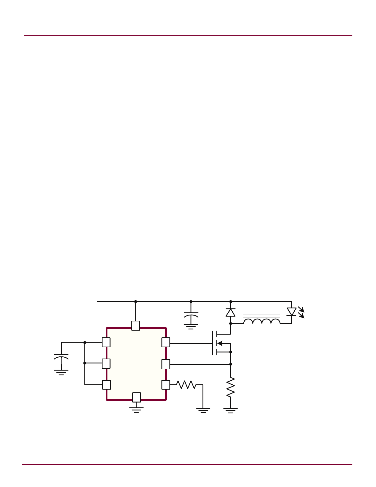
HV9961
VIN
GATEPWMD
LD
VD
D
RT
CS
GN
D
LED
Load
Sets
LED
Curren
t
8.0 - 450VDC
R
CS
R
T
Constant Current Control
HV9961
Features
Fast average current control
►
Programmable constant off-time switching
►
Linear dimming input
►
PWM dimming input
►
Output short circuit protection with skip mode
►
Ambient operating temperature -40OC to +125OC
►
Pin-compatible with the HV9910B
►
Applications
DC/DC or AC/DC LED driver applications
►
LED backlight driver for LCD displays
►
General purpose constant current source
►
LED signage and displays
►
Architectural and decorative LED lighting
►
LED street lighting
►
General Description
The HV9961 is an average current mode control LED driver
IC operating in a constant off-time mode. Unlike HV9910B,
this control IC does not produce a peak-to-average error, and
therefore greatly improves accuracy, line and load regulation
of the LED current without any need for loop compensation or
high-side current sensing. The output LED current accuracy
is ±3%.
The IC is equipped with a current limit comparator for hiccupmode output short circuit protection.
The HV9961 can be powered from an 8.0 - 450V supply.
A PWM dimming input is provided that accepts an external
control TTL compatible signal. The output current can be
programmed by an internal 275mV reference, or controlled
externally through a 0 - 1.5V dimming input.
HV9961 is pin-to-pin compatible with HV9910B and it can
be used as a drop-in replacement for many applications to
improve the LED current accuracy and regulation.
Typical Application Circuit
Page 2
HV9961
Supertex inc. ● 1235 Bordeaux Drive, Sunnyvale, CA 94089 ● Tel: 408-222-8888 ● www.supertex.com
1
2
3
4
5
6
7
8
16
15
14
13
12
11
10
9
8
7
6
5
1
2
3
4
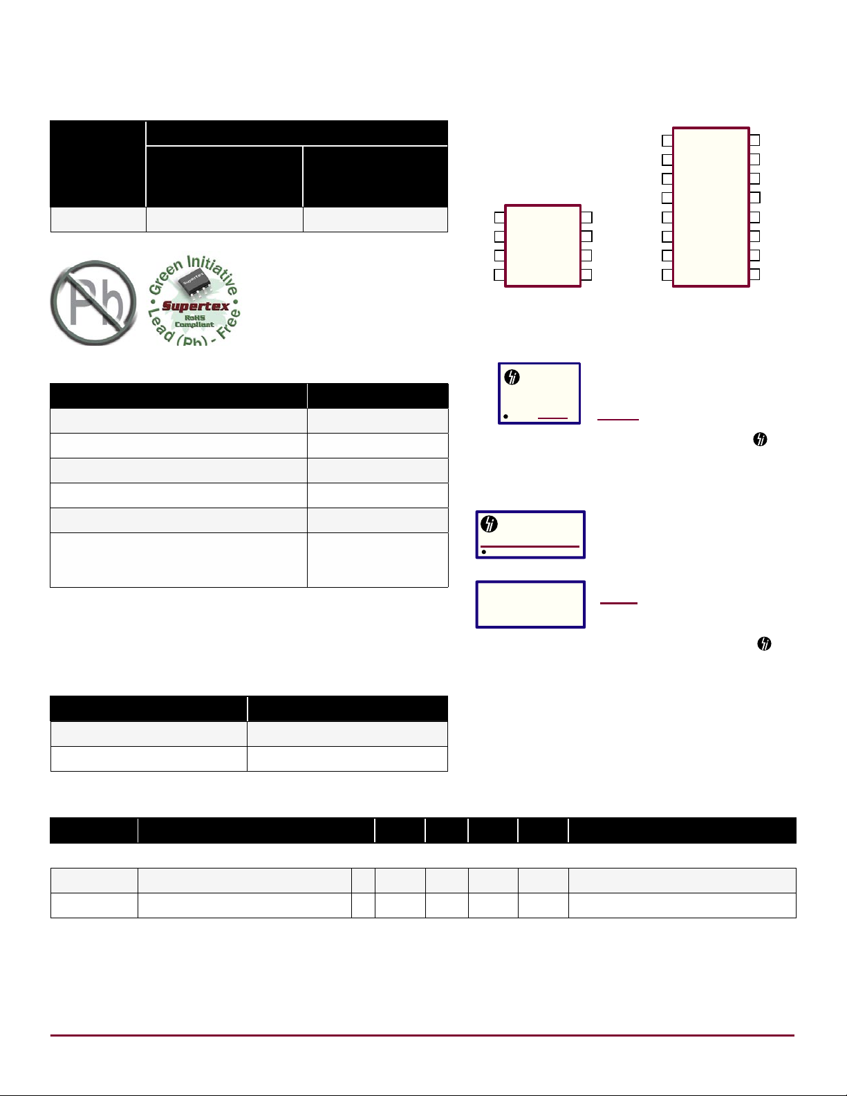
VIN
CS
GND
GATE
RT
LD
VDD
PWMD
VIN
NC
NC
CS
GND
NC
NC
GATE
NC
NC
RT
LD
VDD
NC
NC
PWMD
Y = Last Digit of Year Sealed
WW = Week Sealed
L = Lot Number
= “Green” Packaging
YW W
H9961
LL LL
Y = Last Digit of Year Sealed
WW = Week Sealed
L = Lot Number
C = Country of Origin*
A = Assembler ID*
= “Green” Packaging
*May be part of top marking
Top Marking
Bottom Marking
HV9 961NG
Y WW LLL LLLL L
CCCCCCCCC AAA
Ordering Information
Package Options
Device
8-Lead SOIC
4.90x3.90mm body
1.75mm height (max)
1.27mm pitch
16-Lead SOIC
9.90x3.90mm body
1.75mm height (max)
1.27mm pitch
HV9961 HV9961LG-G HV9961NG-G
-G indicates package is RoHS compliant (‘Green’)
Absolute Maximum Ratings
Parameter Value
VIN to GND -0.5V to +470V
VDD to GND 12V
CS, LD, PWMD, GATE, RT to GND -0.3V to (V
Junction temperature range -40°C to +150°C
DD
+0.3V)
Pin Description
8-Lead SOIC (LG) 16-Lead SOIC (NG)
Product Marking
Package may or may not include the following marks: Si or
8-Lead SOIC (LG)
Storage temperature range -65°C to +150°C
Continuous power dissipation (T
8-Lead SOIC
16-Lead SOIC
Stresses beyond those listed under “Absolute Maximum Ratings” may cause
permanent damage to the device. These are stress ratings only, and functional
operation of the device at these or any other conditions beyond those indicated in
the operational sections of the specifications is not implied. Exposure to absolute
maximum rating conditions for extended periods may affect device reliability.
Thermal Resistance
Package θ
8-Lead SOIC 128OC/W
16-Lead SOIC 82OC/W
Electrical Characteristics (Specifications are at T
Sym Description Min Typ Max Units Conditions
Input
V
INDC
I
INSD
Notes:
1. Also limited by package power dissipation limit, whichever is lower.
* Denotes the specifications which apply over the full operating ambient temperature range of -40°C < TA < +125°C.
= +25°C)
A
650mW
1000mW
Package may or may not include the following marks: Si or
16-Lead SOIC (NG)
JA
= 25°C. VIN = 12V, VLD = VDD, PWMD = VDD unless otherwise noted))
A
Input DC supply voltage range1* 8.0 - 450 V DC input voltage
Shut-down mode supply current * - 0.5 1.0 mA Pin PWMD to GND
2
Page 3
HV9961
Supertex inc. ● 1235 Bordeaux Drive, Sunnyvale, CA 94089 ● Tel: 408-222-8888 ● www.supertex.com
Electrical Characteristics (Specifications are at T
= 25°C. VIN = 12V, VLD = VDD, PWMD = VDD unless otherwise noted))
A
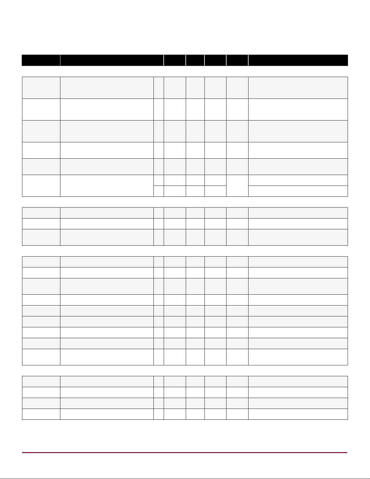
Sym Description Min Typ Max Units Conditions
Internal Regulator
V
DD
ΔV
DD, line
ΔV
DD, load
UVLO
∆UVLO
I
IN,MAX
Internally regulated voltage - 7.25 7.50 7.75 V
Line regulation of V
Load regulation of V
DD
DD
VDD undervoltage lockout
threshold
VDD undervoltage lockout
hysteresis
Maximum input current
(limited by UVLO)
- 0 - 1.0 V
- 0 - 100 mV
* 6.45 6.70 6.95 V VIN rising
- - 500 - mV VIN falling
# 3.5 - -
mA
# 1.5 - - V
V
500pF at GATE; RT = 226kΩ
V
500pF at GATE; RT = 226kΩ
I
500pF at GATE; RT = 226kΩ
V
PWM Dimming
V
V
EN(lo)
EN(hi)
R
EN
PWMD input low voltage * - - 0.8 V V
PWMD input high voltage * 2.2 - - V V
Internal pull-down resistance
at PWMD
- 50 100 150 kΩ V
= 8.0V, I
IN
= 8.0 - 450V, I
IN
DD(ext)
= 8.0V, TA = 25OC
IN
= 8.0V, TA = 125OC
IN
= 8.0 - 450V
IN
= 8.0 - 450V
IN
PWMD
DD(ext)
= 0 - 1.0mA,
= 5.0V
= 0,
DD(ext)
= 0,
Average Current Sense Logic
V
CS
A
V(LD)
AV
LD(OFFSET)
- CS threshold temp regulation * - - 5.0 mV ---
V
LD(OFF)
ΔV
LD(OFF)
T
BLANK
T
ON(min)
D
MAX
Current sense reference voltage - 268 - 286 mV ---
LD-to-CS voltage ratio - 0.182 - 0.188 - ---
LD-to-CS voltage offset - 0 - 10 mV
LD input voltage, shutdown - - 150 - mV VLD falling
LD input voltage, enable - - 200 - mV VLD rising
Current sense blanking interval * 150 - 320 ns ---
Minimum on-time - - - 1000 ns CS = V
Maximum steady-state duty
cycle
- 75 - - %
Short Circuit Protection
V
CS
T
DELAY
T
HICCUP
T
ON(min)
Notes:
* Denotes the specifications which apply over the full operating ambient temperature range of -40°C < T
# Guaranteed by design.
Hiccup threshold voltage - 410 - 470 mV ---
Current limit delay CS-to-GATE - - - 150 ns CS = V
Short circuit hiccup time - 350 - 550 μs ---
Minimum on-time (short circuit) - - - 430 ns CS = V
Offset = V
V
= 1.2V
LD
CS
+30mV
CS
- A
V(LD)
• VLD;
Reduction in output LED current
may occur beyond this duty cycle
+30mV
CS
DD
< +125°C.
A
3
Page 4
HV9961
Supertex inc. ● 1235 Bordeaux Drive, Sunnyvale, CA 94089 ● Tel: 408-222-8888 ● www.supertex.com
CS
RSQ
Q
T
OFF
Timer
L/E
Blanking
GATE
0.44V
MIN (V
LD
• 0.185, 0.275V)
LD
400µs
PWMD
RT
GND
Current
Mirror
i
Regulator
VIN
VDD
UVLO
POR
0.15/0.20V
Average Current
Control Logic
OU
T
Auto-REF
HV9961
CLK
IN
Electrical Characteristics (Specifications are at T
= 25°C. VIN = 12V, VLD = VDD, PWMD = VDD unless otherwise noted))
A
Sym Description Min Typ Max Units Conditions
T
Timer
OFF
T
OFF
Off time
- 8.0 10 12 RT = 226kΩ
- 32 40 48
RT = 1.00MΩ
μs
GATE Driver
I
SOURCE
I
SINK
t
RISE
t
FALL
Notes:
* Denotes the specifications which apply over the full operating ambient temperature range of -40°C < T
# Guaranteed by design.
GATE sourcing current - 0.165 - - A V
GATE sinking current - 0.165 - - A V
GATE output rise time - - 30 50 ns C
GATE output fall time - - 30 50 ns C
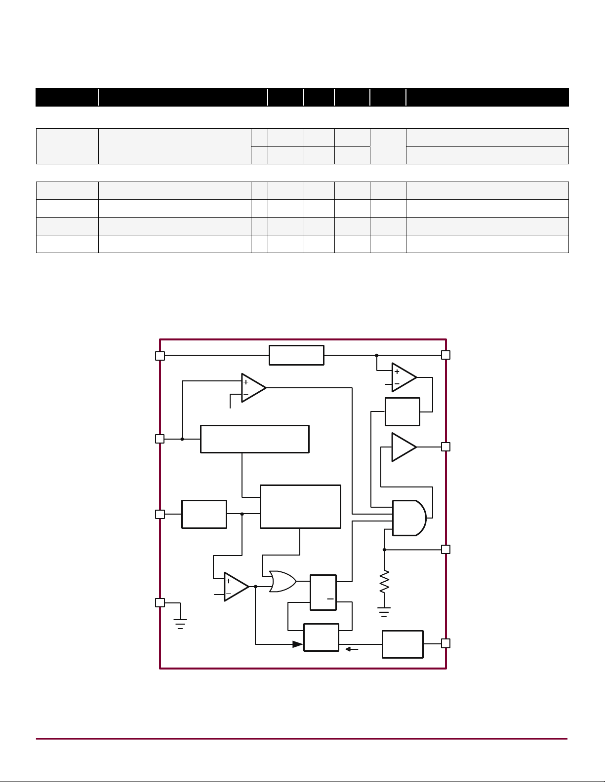
Functional Block Diagram
= 0V, V
GATE
= VDD, V
GATE
= 500pF, V
GATE
= 500pF, V
GATE
< +125°C.
A
DD
DD
= 7.5V
= 7.5V
= 7.5V
DD
= 7.5V
DD
4
Page 5
Supertex inc. ● 1235 Bordeaux Drive, Sunnyvale, CA 94089 ● Tel: 408-222-8888 ● www.supertex.com
Application Information
VIN = 170VDC
HV9961
HV9910B
0 10 20 30 40 50 60
0.60
0.55
0.50
0.45
0.40
0.35
0.30
0.25
LED Current (A)
Output Voltage (V)
Output Characteristics
General Description
Peak-current control (as in HV9910B) of a buck converter is
the most economical and simple way to regulate its output
current. However, it suffers accuracy and regulation problems that arise from the so-called peak-to-average current
error, contributed by the current ripple in the output inductor
and the propagation delay in the current sense comparator. The full inductor current signal is unavailable for direct
sensing at the ground potential in a buck converter when
the control switch is referenced to the same ground potential because the control switch is only conducting for small
periods. While it is very simple to detect the peak current in
the switch, controlling the average inductor current is usually implemented by level translating the sense signal from
+VIN. Though this is practical for relatively low input voltage
VIN, this type of average-current control may become excessively complex and expensive in the offline AC or other highvoltage DC applications.
The HV9961 employs Supertex’ proprietary control scheme,
achieving fast and very accurate control of average current
in the buck inductor through sensing the switch current only.
No compensation of the current control loop is required. The
LED current response to PWMD input is similar to that of the
HV9910B. The inductor current ripple amplitude does not af
fect this control scheme significantly, and therefore, the LED
current is independent of the variation in inductance, switching frequency or output voltage. Constant off-time control of
the buck converter is used for stability and to improve the
LED current regulation over a wide range of input voltages.
(Note that, unlike HV9910B, the HV9961 does not support
the constant-frequency mode of operation.)
OFF Timer
The timing resistor connected to RT determines the off-time
of the gate driver, and it must be wired to GND. (Wiring this
resistor to GATE as with HV9910B is no longer supported.)
The equation governing the off-time of the GATE output is
given by:
T
OFF
(µs) =
within the range of 30kΩ ≤ RT ≤ 1.0MΩ.
RT (kΩ)
+ 0.3 (1)
25
HV9961
feedback operates in a fast open-loop mode. No compensa
tion is required. Output current is programmed simply as:
I
when the voltage at the LD input VLD ≥ 1.5V. Otherwise:
I
R
The above equations are only valid for continuous conduction of the output inductor. It is a good practice to design the
inductor such that the switching ripple current in it is 30~40%
of its average peak-to-peak, full load, DC current. Hence,
the recommended inductance can be calculated as:
LO =
The duty-cycle range of the current control feedback is limited to D ≤ 0.75. A reduction in the LED current may occur
when the LED string voltage VO is greater than 75% of the
input voltage VIN of the HV9961 LED driver.
Reducing the output LED voltage V
D
, where D
MIN
the loss of regulation of the LED current. This condition,
however, causes an increase in the LED current and can
potentially trip the short-circuit protection comparator.
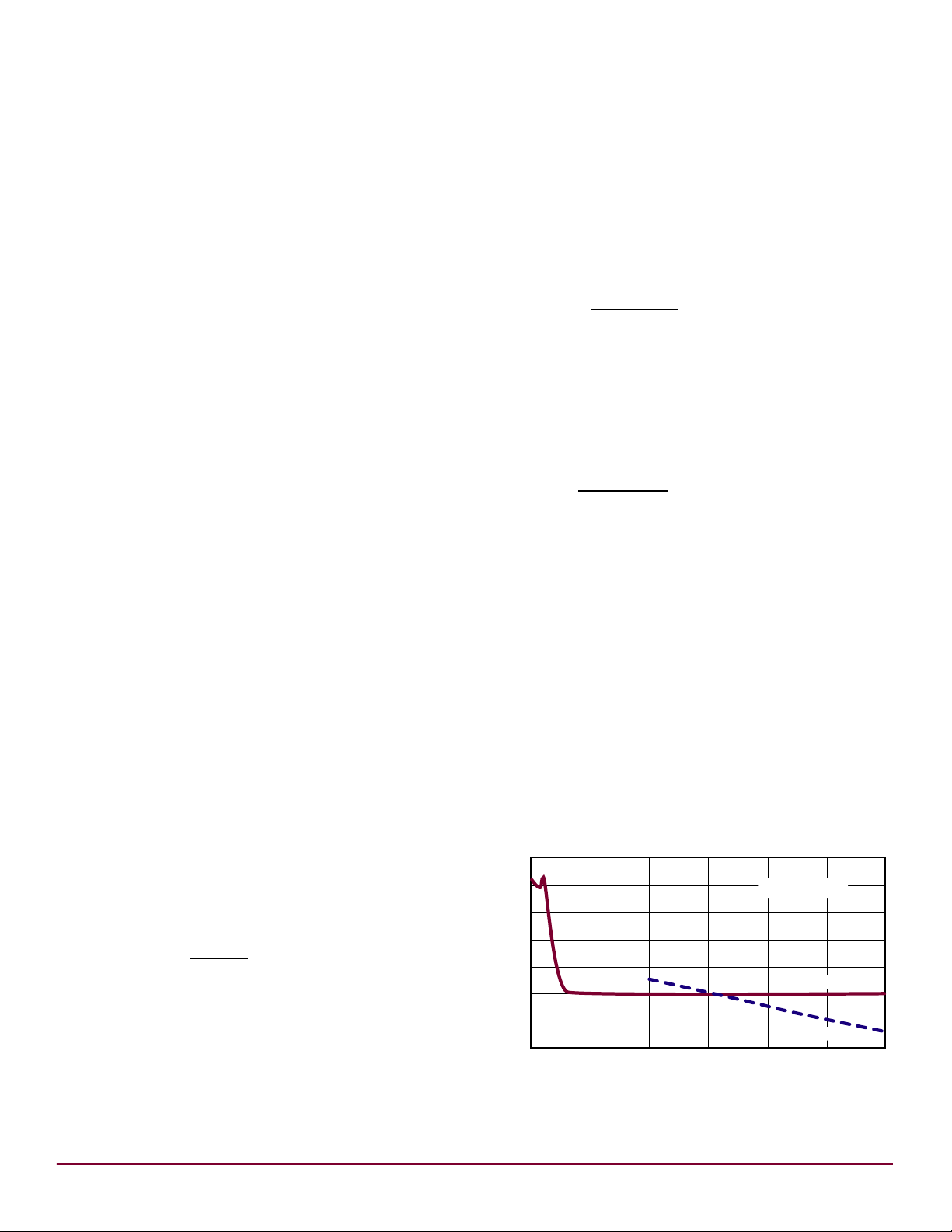
The typical output characteristic of the HV9961 LED driver is
shown in Fig.1. The corresponding HV9910B characteristic
is given for the comparison.
LED
LED
0.275V
=
R
VLD • 0.185
=
V
O(MAX)
0.4 • I
MIN
(2)
CS
(3)
CS
• T
OFF
(4)
O
below V
= 1.0µs/(T
O
+1.0µs), may also result in
OFF
O(MIN)
-
= VIN •
Average Current Control Feedback and Output
Short Circuit Protection
The current through the switching MOSFET source is averaged and used to give constant-current feedback. This current is detected using a sense resistor at the CS pin. The
Fig.1. Typical output characteristic of an HV9961 LED
driver.
5
Page 6
HV9961
Supertex inc. ● 1235 Bordeaux Drive, Sunnyvale, CA 94089 ● Tel: 408-222-8888 ● www.supertex.com
400µs
0.44V/R
CS
0 0.2 0.4 0.6 0.8 1.0 1.2 1.4 1.6
0.40
0.35
0.30
0.25
0.20
0.15
0.10
0.05
0
LED Current (A)
LD (V)
LD Response Characteristics
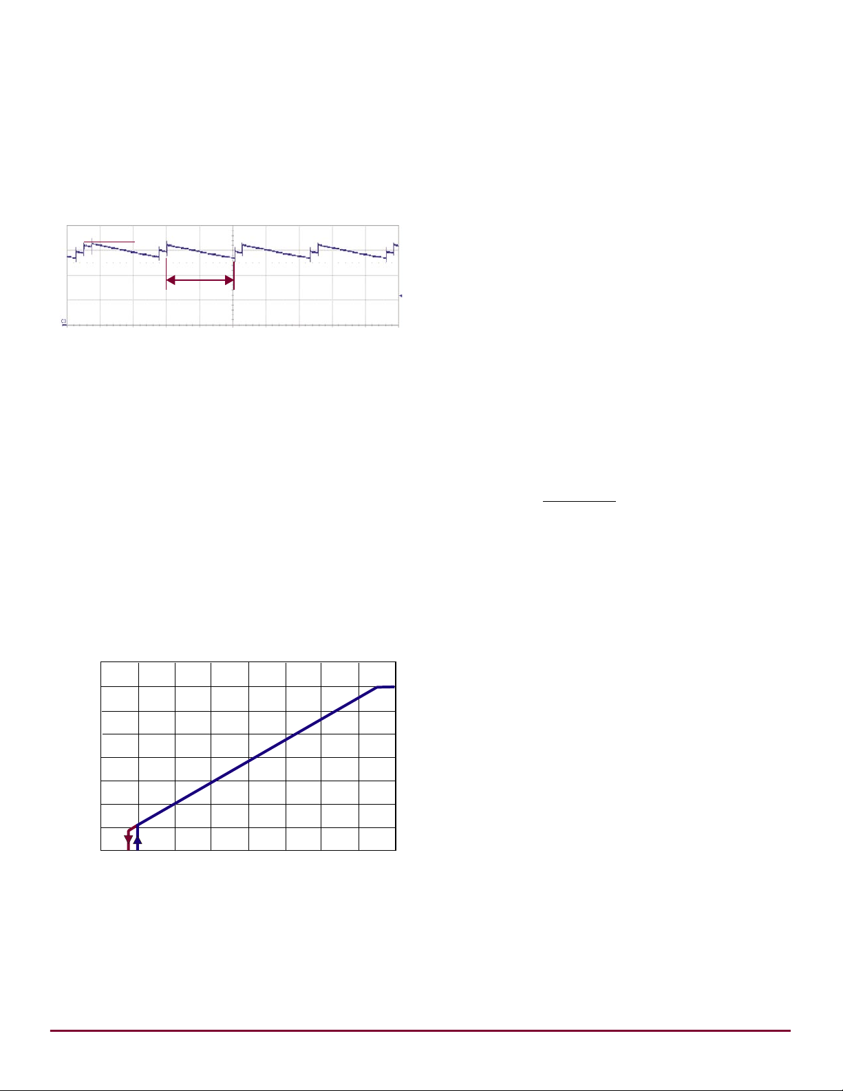
The short circuit protection comparator trips when the voltage at CS exceeds 0.44V. When this occurs, the GATE offtime T
= 400µs is generated to prevent stair-casing
HICCUP
of the inductor current and potentially its saturation due to
insufficient output voltage. The typical short-circuit current is
shown in the waveform of Fig. 2.
Fig.2. Short-circuit inductor current.
A leading-edge blanking delay is provided at CS to prevent
false triggering of the current feedback and the short circuit
protection.
Linear Dimming
When the voltage at LD falls below 1.5V, the internal 275mV
reference to the constant-current feedback becomes overridden by VLD • 0.185. As long as the current in the inductor
remains continuous, the LED current is given by the equation (3) above. However, when VLD falls below 150mV, the
GATE output becomes disabled. The GATE signal recovers,
when VLD exceeds 200mV. This is required in some applications to be able to shut the LED lamp off with the same signal
input that controls the brightness. The typical linear dimming
response is shown in Fig.3.
pulse-width modulated signal of a measured amplitude be
low 1.5V should be applied at LD.
Input Voltage Regulator
The HV9961 can be powered directly from an 8.0 ~ 450VDC
supply through its VIN input. When this voltage is applied at
the VIN pin, the HV9961 maintains a constant 7.5V level at
VDD. This voltage can be used to power the IC and external
circuitry connected to VDD within the rated maximum current or within the thermal ratings of the package, whichever
limit is lower. The VDD pin must be bypassed by a low ESR
capacitor to provide a low impedance path for the high frequency current of the GATE output. The HV9961 can also be
powered through the VDD pin directly with a voltage greater
than the internally regulated 7.5V, but less than 12V.
Despite the instantaneous voltage rating of 450V, continu
ous voltage at VIN is limited by the power dissipation in the
package. For example, when HV9961 draws IIN = 2.0mA
from the VIN input, and the 8-pin SOIC package is used, the
maximum continuous voltage at VIN is limited to:
V
IN(MAX)
=
where the ambient temperature TA = 25OC, the maximum
working junction temperature T
to-ambient thermal resistance R
In such cases, when it is needed to operate the HV9961
from a higher voltage, a resistor or a Zener diode can be
added in series with the VIN input to divert some of the
power loss from the HV9961. In the above example, using
a 100V Zener diode will allow the circuit to work up to 490V.
The input current drawn from the VIN pin is represented by
the following equation:
(T
J(MAX)
R
θ,J-A
- TA )
= 390V (5)
• I
IN
= 125OC, the junction-
J(MAX)
= 128OC/W.
θ,JA
-
-
Fig.3. Typical linear dimming response of an HV9961
The linear dimming input could also be used for “mixedmode” dimming to expand the dimming ratio. In such case a
LED driver
IIN ≈ 1.0mA + QG • fS (6)
In the above equation, f
is the switching frequency, and QG
S
is the GATE charge of the external FET obtained from the
manufacturer’s datasheet.
GATE Output
The GATE output of the HV9961 is used to drive an external
MOSFET. It is recommended that the gate charge QG of the
external MOSFET be less than 25nC for switching frequencies ≤100kHz and less than 15nC for switching frequencies
>100kHz.
6
Page 7
HV9961
Supertex inc. ● 1235 Bordeaux Drive, Sunnyvale, CA 94089 ● Tel: 408-222-8888 ● www.supertex.com
PWM Dimming
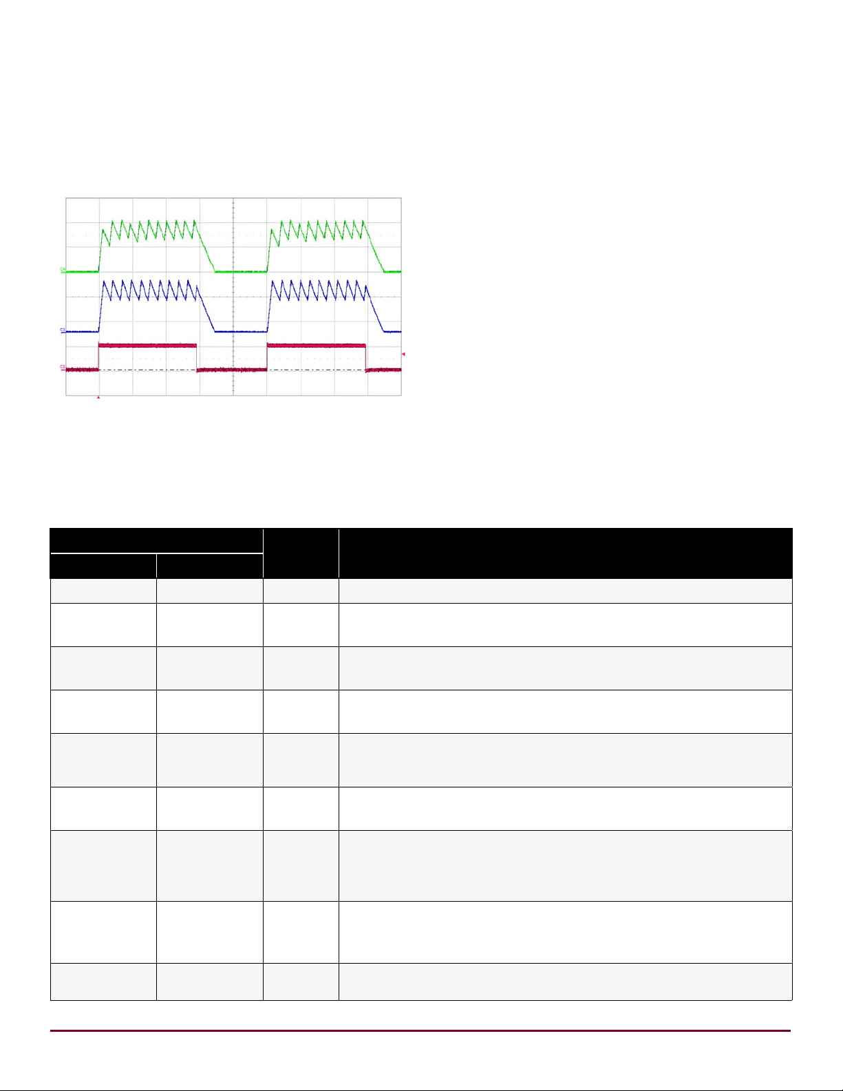
Due to the fast open-loop response of the average-current
control loop of the HV9961, its PWM dimming performance
nearly matches that of the HV9910B. The inductor current
waveform comparison is shown in Fig. 4.
Fig.4. Typical PWM dimming response of an HV9961
LED driver.
[CH2 (red): PWMD; CH4 (green): Inductor Current; CH3 (blue):
Same as HV9910B for comparison]
The rising and falling edges are limited by the current slew
rate in the inductor. The first switching cycle is terminated
upon reaching the 275mV (VLD • 0.185) level at CS. The circuit is further reaching its steady-state within 3~4 switching
cycles regardless of the switching frequency.
Pin Description
Pin #
8-Lead SOIC 16-Lead SOIC
1 1 VIN This pin is the input of an 8.0 - 450V linear regulator.
2 4 CS
3 5 GND
4 8 GATE
5 9 PWMD
6 12 VDD
7 13 LD
Function Description
This pin is the current sense pin used to sense the FET current by means
of an external sense resistor.
Ground return for all internal circuitry. This pin must be electrically con
nected to the ground of the power train.
This pin is the output GATE driver for an external N-channel power
MOSFET.
This is the PWM dimming input of the IC. When this pin is pulled to GND,
the gate driver is turned off. When the pin is pulled high, the gate driver
operates normally.
This is the power supply pin for all internal circuits. It must be bypassed
with a low ESR capacitor to GND (at least 0.1μF).
This pin is the linear dimming input, and it sets the current sense threshold as long as the voltage at this pin is less than 1.5V. If voltage at LD falls
below 150mV, the GATE output is disabled. The GATE signal recovers at
200mV at LD.
-
8 14 RT
-
2, 3, 6, 7, 10,
11, 15, 16
NC No connection
A resistor connected between this pin and GND programs the GATE offtime.
7
Page 8
Supertex inc. ● 1235 Bordeaux Drive, Sunnyvale, CA 94089 ● Tel: 408-222-8888 ● www.supertex.com
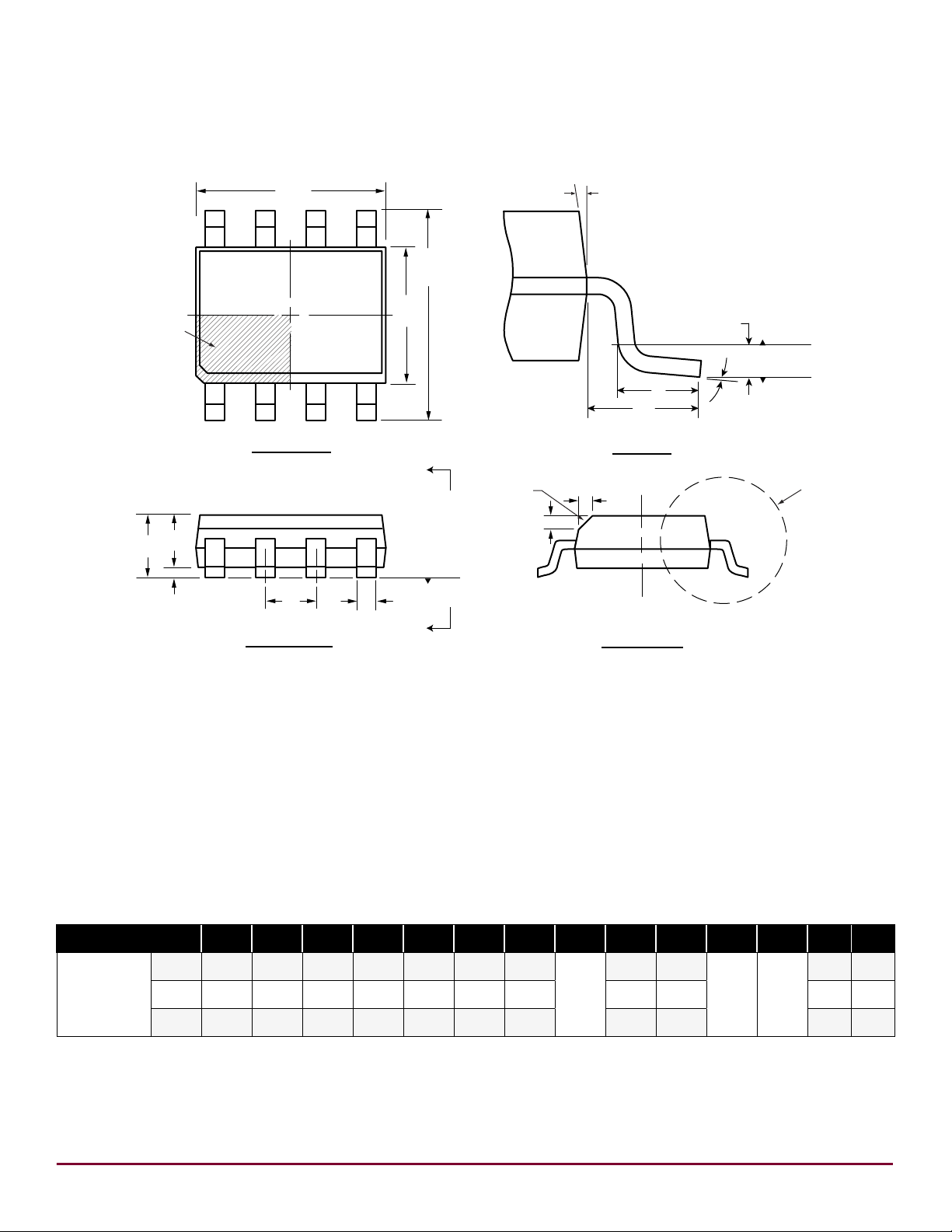
8-Lead SOIC (Narrow Body) Package Outline (LG)
1
8
Seating
Plane
Gauge
Plane
L
L1
L2
E
E1
D
e
b
A
A2
A1
Seating
Plane
A
A
Top View
Side View
View B
View B
θ1
θ
Note 1
(Index Area
D/2 x E1/2)
View A-A
h
h
Note 1
4.90x3.90mm body, 1.75mm height (max), 1.27mm pitch
HV9961
Note:
This chamfer feature is optional. A Pin 1 identifier must be located in the index area indicated. The Pin 1 identifier can be: a molded mark/identifier;
1.
an embedded metal marker; or a printed indicator.
Symbol A A1 A2 b D E E1 e h L L1 L2 θ θ1
MIN 1.35* 0.10 1.25 0.31 4.80* 5.80* 3.80*
Dimension
(mm)
JEDEC Registration MS-012, Variation AA, Issue E, Sept. 2005.
* This dimension is not specified in the JEDEC drawing.
Drawings are not to scale.
Supertex Doc. #: DSPD-8SOLGTG, Version I041309.
NOM - - - - 4.90 6.00 3.90 - - - -
MAX 1.75 0.25 1.65* 0.51 5.00* 6.20* 4.00* 0.50 1.27 8
8
1.27
BSC
0.25 0.40
1.04
REF
0.25
BSC
O
0
O
5
O
15
O
Page 9
Supertex inc. does not recommend the use of its products in life support applications, and will not knowingly sell them for use in such applications unless it receives
an adequate “product liability indemnification insurance agreement.”
Supertex inc. does not assume responsibility for use of devices described, and limits its liability
to the replacement of the devices determined defective due to workmanship. No responsibility is assumed for possible omissions and inaccuracies. Circuitry an
d
specifications are subject to change without notice. For the latest product specifications refer to the
Supertex inc. (website: http//www.supertex.com)
©2010 Supertex inc. All rights reserved. Unauthorized use or reproduction is prohibited.
Supertex inc.
1235 Bordeaux Drive, Sunnyvale, CA 94089
Tel: 408-222-8888
www.supertex.com
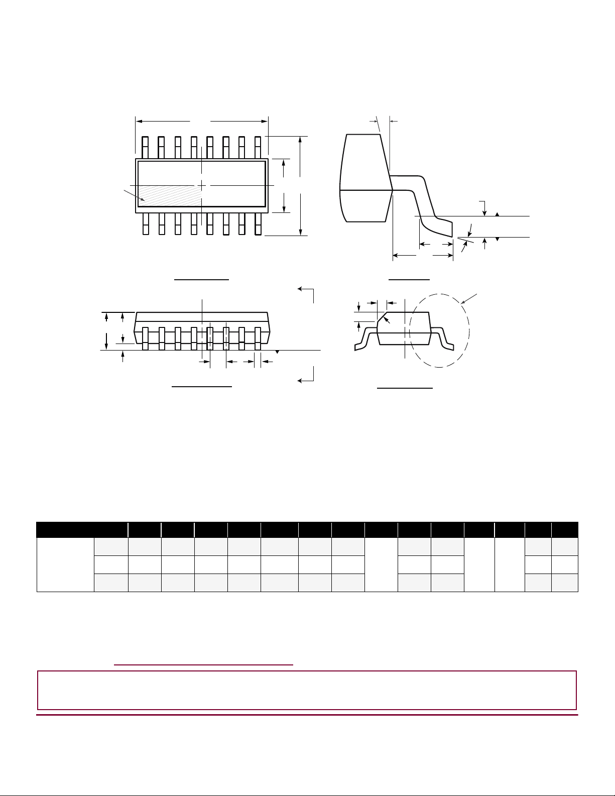
16-Lead SOIC (Narrow Body) Package Outline (NG)
D
Seating
Plane
Gauge
Plane
L
L1
L2
Top View
Side View
View A-A
View B
View
B
θ1
θ
E1
E
A
A2
A1
A
A
Seating
Plane
e
b
h
h
16
1
Note 1
Note 1
(Index Area
D/2 x E1/2)
9.90x3.90mm body, 1.75mm height (max), 1.27mm pitch
HV9961
Note:
This chamfer feature is optional. If it is not present, then a Pin 1 identifier must be located in the index area indicated. The Pin 1 identifier can be:
1.
a molded mark/identifier; an embedded metal marker; or a printed indicator.
Symbol A A1 A2 b D E E1 e h L L1 L2 θ θ1
Dimension
(mm)
JEDEC Registration MS-012, Variation AC, Issue E, Sept. 2005.
* This dimension is not specified in the JEDEC drawing.
Drawings are not to scale.
Supertex Doc. #: DSPD-16SONG, Version G041309.
MIN 1.35* 0.10 1.25 0.31 9.80* 5.80* 3.80*
NOM - - - - 9.90 6.00 3.90 - - - -
MAX 1.75 0.25 1.65* 0.51 10.00* 6.20* 4.00* 0.50 1.27 8O15
(The package drawing(s) in this data sheet may not reflect the most current specifications. For the latest package outline
1.27
BSC
0.25 0.40
1.04
REF
0.25
BSC
information go to http://www.supertex.com/packaging.html.)
Doc.# DSFP-HV9961
B101510
9
O
0
O
5
O
 Loading...