

Page 1
● 1235 Bordeaux Drive, Sunnyvale, CA 94089 ● Tel: 408-222-8888 ● www.supertex.com
Programmable-Current LED Lamp Driver IC
with PWM Dimming
HV9925
Features
Programmable output current to 50mA
►
PWM dimming / enable
►
Universal 85 - 264VAC operation
►
Fixed off-time buck converter
►
Internal 475V power MOSFET
►
Over-temperature protection with hysteresis
►
Applications
Decorative lighting
►
Low power lighting fixtures
►
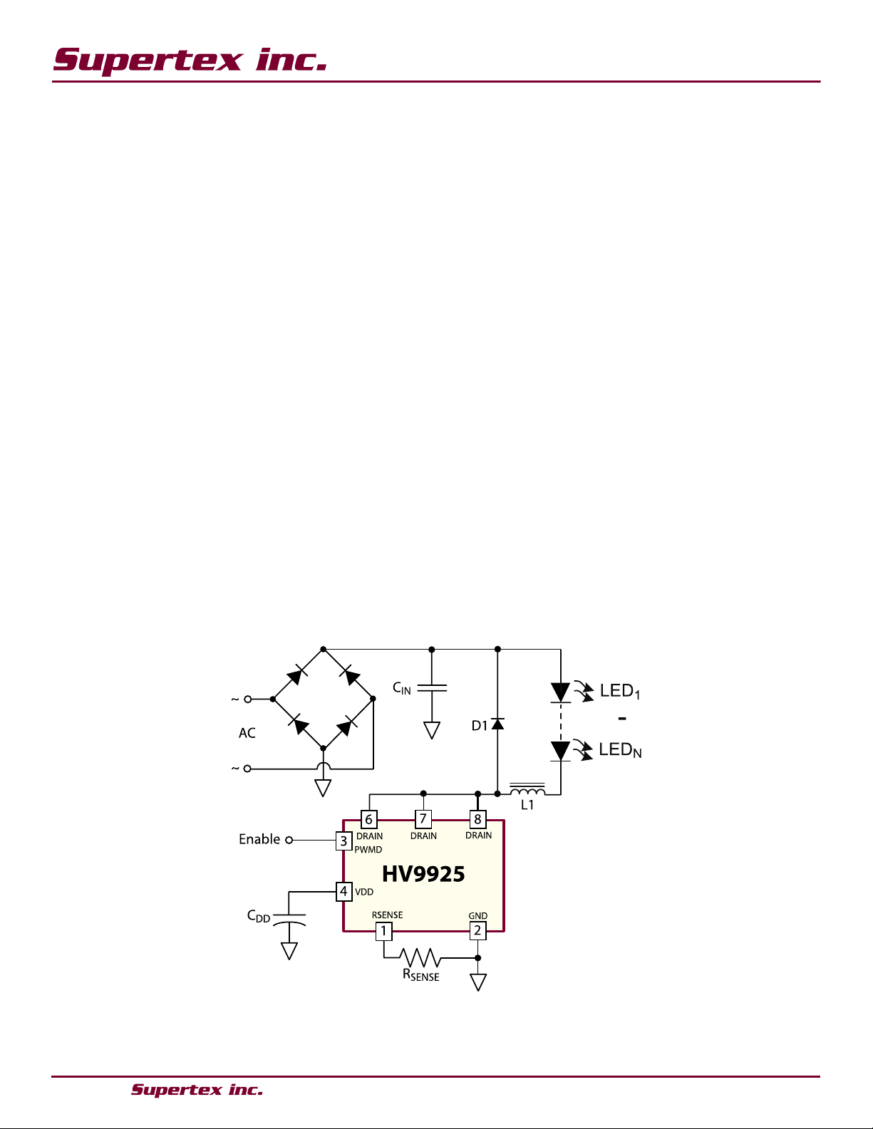
Typical Application Circuit
General Description
The HV9925 is a pulse width modulated (PWM) high-efficiency
LED driver control IC with PWM dimming capabilities. It
allows efficient operation of high brightness LED strings from
voltage sources ranging up to 400VDC. The HV9925 includes
an internal high-voltage switching MOSFET controlled with a
fixed off-time (T
is driven at constant current, thus providing constant light
output and enhanced reliability. Selecting a value of a current
sense resistor can externally program the output LED current
of the HV9925.
The peak current control scheme provides good regulation
of the output current throughout the universal AC line voltage
range of 85 to 264VAC or DC input voltage of 20 to 400V.
The HV9925 is designed with a built in thermal shutdown to
prevent excessive power dissipation in the IC.
) of approximately 10.5µs. The LED string
OFF
Page 2
● 1235 Bordeaux Drive, Sunnyvale, CA 94089 ● Tel: 408-222-8888 ● www.supertex.com
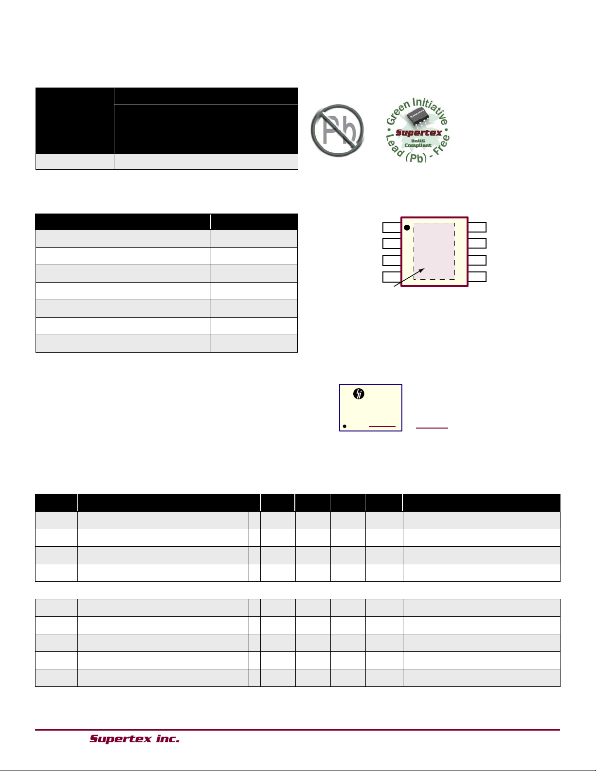
Ordering Information
Y = Year Sealed
WW = Week Sealed
L = Lot Number
= “Green” Packaging
YW W
H9925
L L LL
1
2
3
4
8
7
6
5
RSENSE
GND
PWMD
VDD
DRAIN
DRAIN
DRAIN
NC
Heat Slug
HV9925
Package Option
Device
8-Lead SOIC (w/Heat Slug)
4.90x3.90mm body
1.70mm height (max)
1.27mm pitch
HV9925 HV9925SG-G
-G indicates package is RoHS compliant (‘Green’)
Absolute Maximum Ratings
Parameter Value
Supply voltage, V
PWMD, R
SENSE
Supply current, I
DD
voltage -0.3 to +10V
DD
Operating ambient temperature range -40°C to +85°C
Operating junction temperature range -40°C to +125°C
Storage temperature range -65°C to +150°C
Power dissipation @ 25°C 800mW**
All voltages referenced to GND pin.
**The power dissipation is given for the standard minimum pad without a heat
slug, and based on R
and case-to-ambient thermal resistance, where the latter is determined by
the user’s board design. The junction-to-ambient thermal resistance is R
105°C/W when the part is mounted on a 0.04 in
R
= 60°C/W when mounted on a 1.0in2 pad of 1 oz copper.
θJA
= 125°C/W. R
θJA
is the sum of the junction-to-case
θJA
2
pad of 1 oz copper, and
-0.3 to +10V
+5mA
θJA
Pin Configuration
8-Lead SOIC (SG)
(top view)
Heat slug is at ground potential.
Product Marking
=
8-Lead SOIC (SG)
Electrical Characteristics (The specifications are at T
Sym Parameter Min Typ Max Units Conditions
V
V
ΔV
Output (DRAIN)
V
V
R
C
I
Notes:
* Denotes the specifications which apply over the full operating ambient temperature range of -40°C < T
# Denotes guaranteed by design.
VDD regulator output - - 7.5 - V ---
DD
UVLOVDD
UVLOVDD
I
DD
BR
DRAINVDRAIN
ON
DRAIN
SAT
undervoltage threshold - 4.8 - - V -- undervoltage lockout hysteresis - - 200 - mV ---
Operating supply current - - 300 500 μA V
Breakdown voltage * 475 - - V ---
supply voltage - 20 - - V --On-resistance - - 100 200 Ω I
Output capacitance # - 1.0 5.0 pF V
DRAIN saturation current - 100 150 - mA ---
= 25°C and V
A
2
= 50V, unless otherwise noted.)
DRAIN
DD(EXT)
= 50mA
DRAIN
DRAIN
< +85°C.
A
= 8.5V
= 400V
Page 3
HV9925
● 1235 Bordeaux Drive, Sunnyvale, CA 94089 ● Tel: 408-222-8888 ● www.supertex.com
Electrical Characteristics (cont.) (The specifications are at T
= 25°C and V
A
= 50V, unless otherwise noted.)
DRAIN
Sym Parameter Min Typ Max Units Conditions
Current Sense Comparator
V
T
BLANK
T
ON(MIN)
Threshold voltage - 0.435 0.470 0.525 V ---
TH
Leading edge blanking delay # 200 300 400 ns --Minimum on time - - - 650 ns ---
Off-Time Generator
T
Off time - 8.0 10.5 13 μs ---
OFF
PWM Dimming
V
PWMD,HI
V
PWMD,LO
R
PWMD input high voltage - 2.0 - - V --PWMD input low voltage - - - 0.8 V --PWMD pull down resistance - 100 200 300 kΩ V
PWMD
PWMD
Thermal Shutdown
T
T
Notes:
* Denotes the specifications which apply over the full operating ambient temperature range of -40°C < T
# Denotes guaranteed by design.
Over temperature trip limit # - 140 - °C ---
OT
Temperature hysteresis # - 60 - °C ---
HYST
< +85°C.
A
= 5.0V
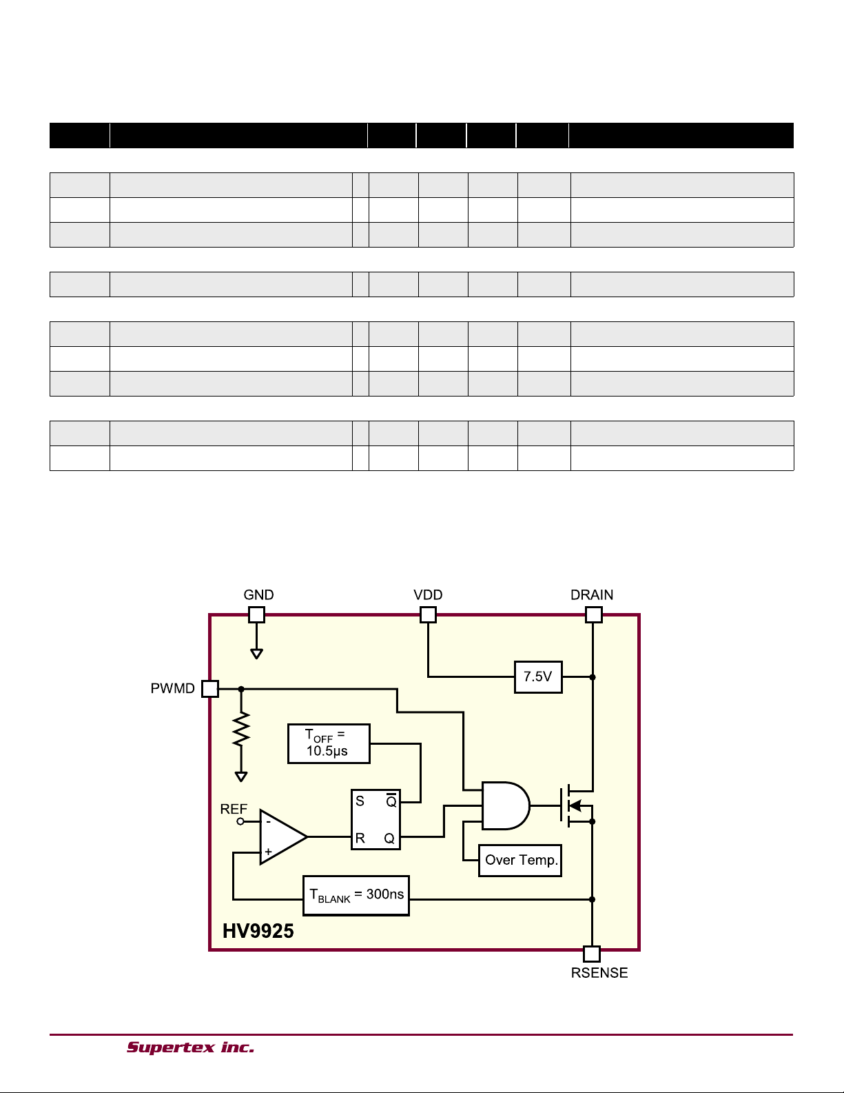
Functional Block Diagram
3
Page 4
HV9925
● 1235 Bordeaux Drive, Sunnyvale, CA 94089 ● Tel: 408-222-8888 ● www.supertex.com
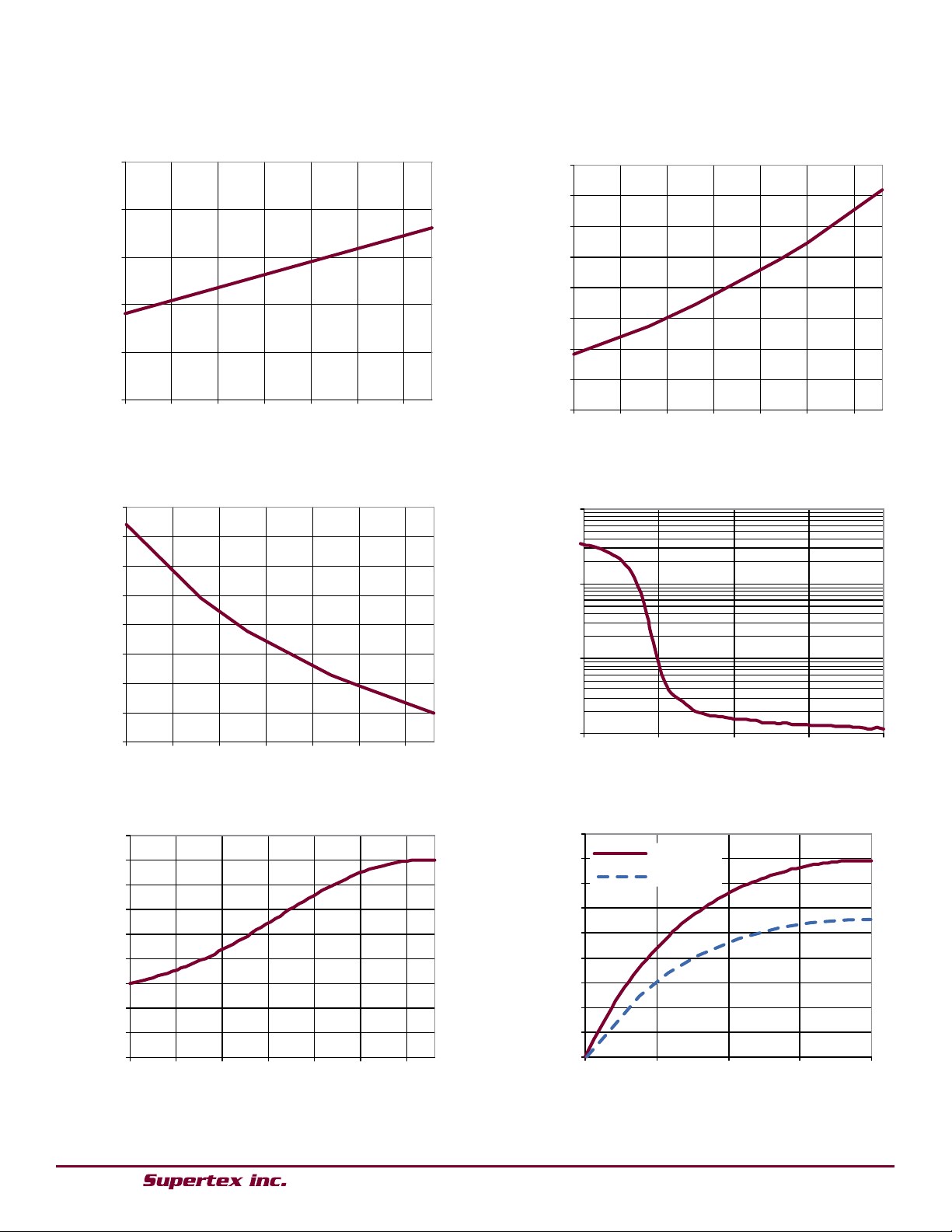
Threshold Voltage VTH vs Temperature T
J
ON Resistance R
ON
vs Temperature T
J
OFF Time T
OFF
vs Temperature T
J
Output Capacitance C
DRAIN
vs V
DRAIN
DRAIN Breakdown Voltage BV vs T
J
Output Characteristics I
DRAIN
vs V
DRAIN
490
500
510
520
530
540
550
560
570
580
-40 -15 10 35 60 85 11
0
Junction Te m perature, °C
DRAIN Breakdown Voltage, V
0
20
40
60
80
10
0
120
14
0
16
0
18
0
0 10 20 30 4
0
DRAIN Voltage , V
DRAIN Current, mA
1
10
10
0
1000
0 10 20 30 4
0
DRAIN Voltage, V
DRAIN Capacitance, pF
0.460
0.465
0.470
0.475
0.480
0.485
-40 -15 10 35 60 85 110
Junction Temperature, °C
Current Sense Threshold, V
9.0
9.
5
10.
0
10.
5
11.
0
11.5
12.
0
12.
5
13.
0
-40 -15 10 35 60 85 11
0
Junction Temperature, °C
OFF Ti m e, μs
40
60
80
10
0
12
0
14
0
16
0
18
0
20
0
-40 -15 10 35 60 85 110
Junction Temperature, °C
ON Resistance, Ohm
TJ = 25OC
TJ = 125OC
Typical Performance Characteristics (T
= 25OC unless otherwise noted)
J
4
Page 5

● 1235 Bordeaux Drive, Sunnyvale, CA 94089 ● Tel: 408-222-8888 ● www.supertex.com
Functional Description
The HV9925 is a PWM peak current control IC for driving
a buck converter topology in continuous conduction mode
(CCM). The HV9925 controls the output current (rather than
output voltage) of the converter that can be programmed by
a single external resistor (R
string of light emitting diodes (LED). An external enable input
(PWMD) is provided that can be utilized for PWM dimming of
an LED string. The typical rising and falling edge transitions
of the LED current when using the PWM dimming feature of
the HV9925 are shown in Fig. 6 and Fig. 7.
When the input voltage of 20 to 400V appears at the DRAIN
pin, the internal linear regulator seeks to maintain a voltage
of 7.5VDC at the V
pin. Until this voltage exceeds the
DD
internally programmed under-voltage threshold, no output
switching occurs. When the threshold is exceeded, the
integrated high-voltage switch turns on, pulling the DRAIN
low. A 200mV hysteresis is incorporated with the undervoltage comparator to prevent oscillation.
When the voltage at R
SENSE
off and the DRAIN output becomes high impedance. At the
same time, a one-shot circuit is activated that determines
the off-time of the switch (10.5µs typ.).
), for the purpose of driving a
SENSE
exceeds 0.47V, the switch turns
HV9925
Adding a filter capacitor across the LED string can reduce
the output current ripple even further, thus permitting a
reduced value of L1. However, one must keep in mind that
the peak-to-average current error is affected by the variation
. Therefore, the initial output current accuracy might
of T
OFF
be sacrificed at large ripple current in L1.
Another important aspect of designing an LED driver with
HV9925 is related to certain parasitic elements of the
circuit, including distributed coil capacitance of L1, junction
capacitance, and reverse recovery of the rectifier diode D1,
capacitance of the printed circuit board traces C
capacitance C
of the controller itself. These parasitic
DRAIN
elements affect the efficiency of the switching converter and
could potentially cause false triggering of the current sense
comparator if not properly managed. Minimizing these
parasitics is essential for efficient and reliable operation of
HV9925.
Coil capacitance of inductors is typically provided in the
manufacturer’s data books either directly or in terms of the
self-resonant frequency (SRF).
SRF = 1 / (2π√(L • C
))
L
and output
PCB
A “blanking” delay of 300ns is provided upon the turn-on of
the switch that prevents false triggering of the current sense
comparator due to the leading edge spike caused by circuit
parasitics.
Application Information
Selecting L1 and D1
The required value of L1 is inversely proportional to the ripple
current ∆I
20~30% is a good practice to ensure noise immunity of the
current sense comparator.
L1 = (VO • T
VO is the forward voltage of the LED string. T
time of the HV9925. The output current in the LED string (IO)
is calculated then as:
IO = (VTH / R
where V
R
SENSE
introduces a peak-to-average error in the output current
setting that needs to be accounted for. Due to the constant
off-time control technique used in the HV9925, the ripple
current is nearly independent of the input AC or DC voltage
variation. Therefore, the output current will remain unaffected
by the varying input voltage.
in it. Setting the relative peak-to-peak ripple to
O
) / ΔIO (1)
OFF
is the off-
OFF
) - 1/2ΔIO (2)
SENSE
is the current sense comparator threshold, and
TH
is the current sense resistor. The ripple current
where L is the inductance value, and C
is the coil capacitance.
L
Charging and discharging this capacitance every switching
cycle causes high-current spikes in the LED string. Therefore,
connecting a small capacitor CO (~10nF) is recommended to
bypass these spikes.
Using an ultra-fast rectifier diode for D1 is recommended to
achieve high efficiency and reduce the risk of false triggering
of the current sense comparator. Using diodes with shorter
reverse recovery time
trr, and lower junction capacitance CJ,
achieves better performance. The reverse voltage rating VR
of the diode must be greater than the maximum input voltage
of the LED lamp.
The total parasitic capacitance present at the DRAIN output
of the HV9925 can be calculated as:
CP = C
When the switch turns on, the capacitance C
DRAIN
+ C
+ CL + CJ (3)
PCB
is discharged
P
into the DRAIN output of the IC. The discharge current is
limited to about 150mA typically. However, it may become
lower at increased junction temperature. The duration of the
leading edge current spike can be estimated as:
T
= ((VIN • CP) / I
SPIKE
) + trr (4)
SAT
5
Page 6
HV9925
● 1235 Bordeaux Drive, Sunnyvale, CA 94089 ● Tel: 408-222-8888 ● www.supertex.com
0 0.1 0.2 0.3 0.4 0.5 0.6 0.7
0.1
0.2
0.3
0.4
0.5
0.6
0.7
KDDM( )
KCDM( )
D
M
In order to avoid false triggering of the current sense
comparator, CP must be minimized in accordance with the
following expression:
(5)
where T
V
BLANK(MIN)
is the maximum instantaneous input voltage.
IN(MAX)
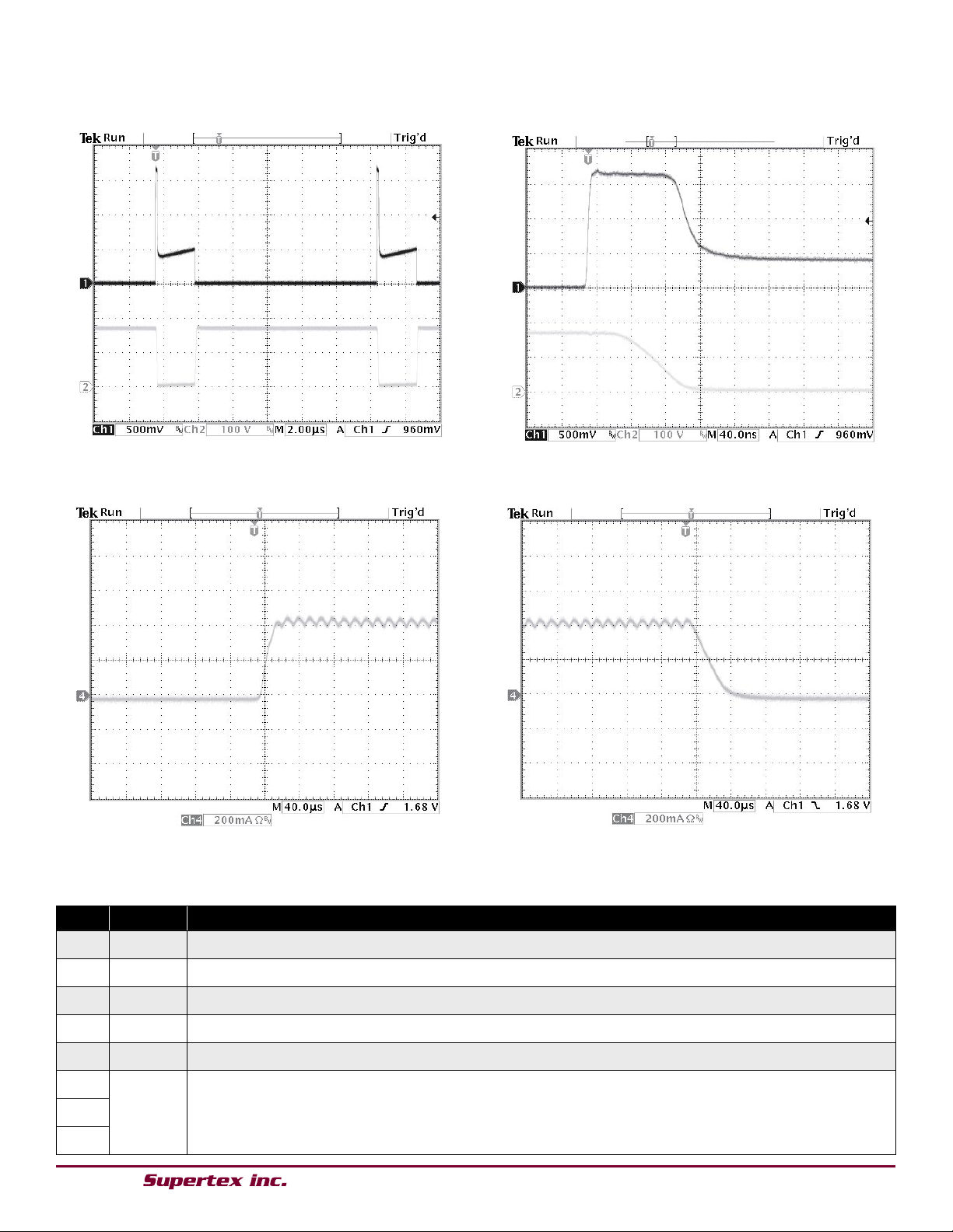
The typical DRAIN and R
is the minimum blanking time of 200ns, and
voltage waveforms are shown
SENSE
in Fig. 3 and Fig. 4.
Estimating Power Loss
Discharging the parasitic capacitance C
into the DRAIN
P
output of the HV9925 is responsible for the bulk of the
switching power loss. It can be estimated using the following
equation:
(6)
where FS is the switching frequency and I
is the saturated
SAT
DRAIN current of the HV9925. The switching loss is the
greatest at the maximum input voltage.
When the LED driver is powered from the full-wave
rectified AC line input, the exact equation for calculating the
conduction loss is more cumbersome. However, it can be
estimated using the following equation:
P
= (KC • I
COND
where V
AC
2
• RON) + (KD • IDD • VAC) (10)
O
is the input AC line voltage. The coefficients KC
and Kd can be determined from the minimum duty ratio
Dm=0.71Vo/(VAC).
Disregarding the voltage drop at HV9925 and D1, the
switching frequency is given by the following:
V
- V
IN
FS =
V
O
(7)
• T
IN
OFF
When the HV9925 LED driver is powered from the full-wave
rectified AC input, the switching power loss can be estimated
as:
VAC is the input AC line voltage.
The switching power loss associated with turn-off transitions
of the DRAIN output can be disregarded. Due to the large
amount of parasitic capacitance connected to this switching
node, the turn-off transition occurs essentially at zerovoltage.
When the HV9925 LED driver is powered from DC input
voltages, conduction power loss can be calculated as:
P
COND
= (D • I
2
• RON) + IDD • VIN • (1 - D) (9)
O
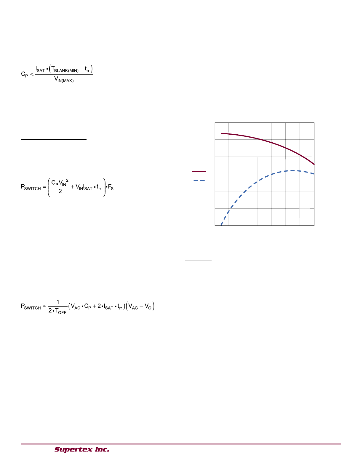
Figure 1. Conduction Loss Coefficients KC and K
EMI Filter
As with all off-line converters, selecting an input filter is critical
to obtaining good EMI. A switching side capacitor, albeit of
small value, is necessary in order to ensure low impedance
to the high frequency switching currents of the converter. As
a rule of thumb, this capacitor should be approximately 0.1-
0.2 µF/W of LED output power. A recommended input filter is
(8)
shown in Figure 2 for the following design example.
Design Example 1
Let us design an HV9925 LED lamp driver meeting the
following specifications:
Input: Universal AC, 85-264VAC
Output Current: 20mA
Load: String of 10 LED (LW541C by OSRAM
VF = 4.1V max. each)
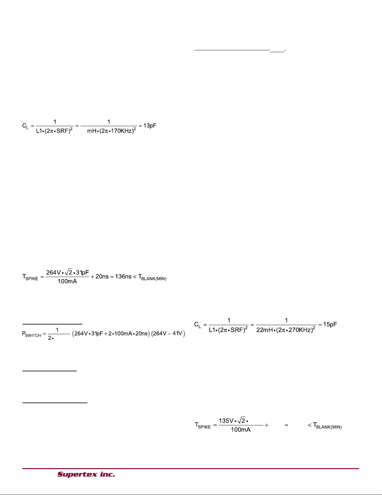
The schematic diagram of the LED driver is shown in
Figure 2.
d
where D = V
/VIN is the duty ratio, RON is the ON resistance,
O
IDD is the internal linear regulator current.
6
Page 7
HV9925
● 1235 Bordeaux Drive, Sunnyvale, CA 94089 ● Tel: 408-222-8888 ● www.supertex.com
68
10.5µs
33ns
102ns
33pF
Step 1. Calculating L1.
The output voltage V
= 10 · VF ≈ 41V (max.). Use equation
O
(1) assuming a 30% peak-to-peak ripple.
L1 = (41V • 10.5µs) / (0.3 • 20mA) = 72mH
Select L1 68mH, I=30mA. Typical SRF = 170KHz. Calculate
the coil capacitance.
Step 2. Selecting D1
Usually, the reverse recovery characteristics of ultrafast rectifiers at I
= 20~50mA are not provided in the
F
manufacturer’s data books. The designer may want to
experiment with different diodes to achieve the best result.
Select D1 MUR160 with V
= 600V, t
R
≈ 20ns (IF = 20mA, I
rr
RR
= 100mA) and CJ ≈ 8pF (VF>50V).
Step 3. Calculate total parasitic capacitance using (3):
CP = 5pF + 5pF +13pF + 8pF = 31pF
Total power dissipation at V
P
= 130mW + 50mW = 180mW
TOTAL
Step 6. Selecting input capacitor C
AC(max)
:
IN
Output Power = 41V • 20mA = 820mW
Select C
ECQ-E4104KF by Panasonic (0.1µF, 400V,
IN
Metalized Polyester Film).
Design Example 2
Let us now design a PWM-dimmable LED lamp driver using
the HV9925:
Input: Universal AC, 85-135VAC
Output Current: 50mA
Load: String of 12 LED (Power TOPLED
®
by
OSRAM, VF = 2.5V max. each)
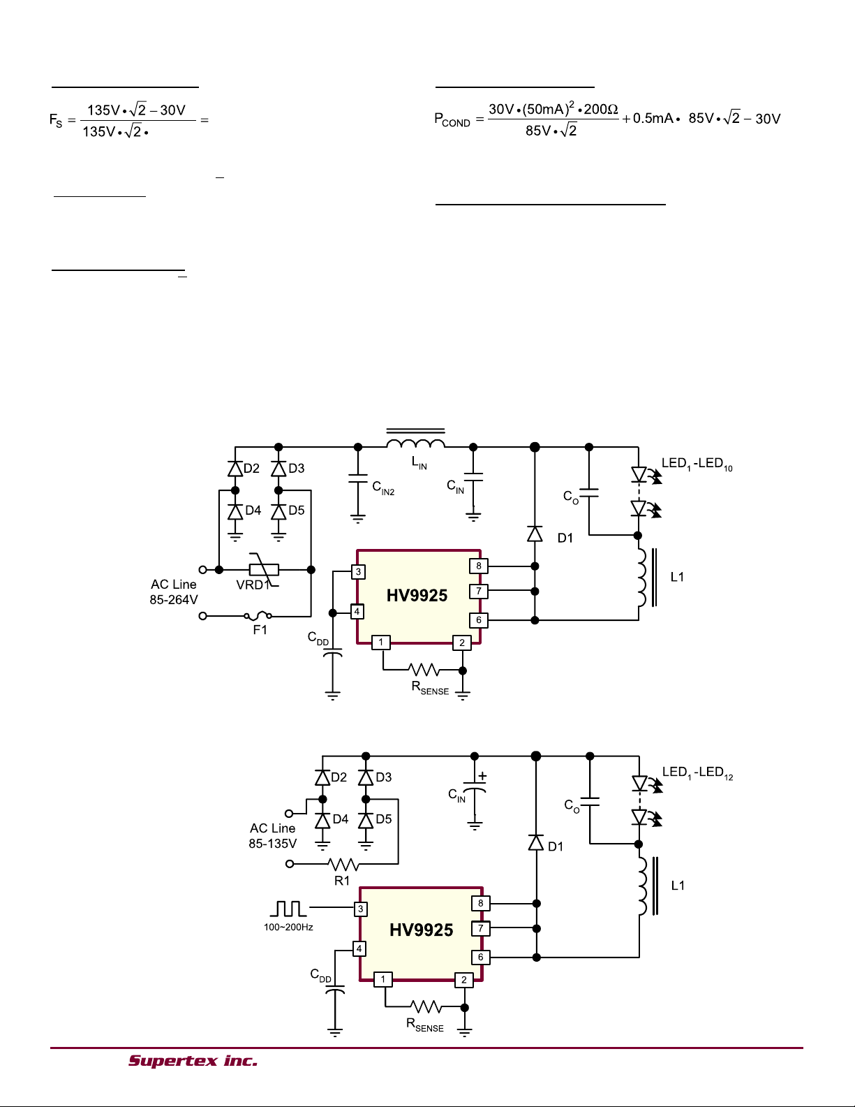
The schematic diagram of the LED driver is shown in Fig.3.
We will use an aluminum electrolytic capacitor for C
in order
IN
to prevent interruptions of the LED current at zero crossings
of the input voltage. As a “rule of thumb”, 2~3μF per each
watt of the input power is required for CIN in this case.
Step 4. Calculating the leading edge spike duration using
(4) and (5):
Step 5. Estimating power dissipation in HV9925 at 264VAC
using (8) and (10)
Switching power loss:
P
≈ 130mW
SWITCH
Minimum duty ratio:
DM = (0.71 • 41V) / 264V ≈ 0.11
Conduction power loss:
P
=
COND
0.20 • (20mA)2 • 210Ω + 0.63 • 200µA • 264V ≈ 50mW
Step 1. Calculating L1.
The output voltage V
= 12 · VF = 30V (max.). Use equation
O
(1) assuming a 30% peak-to-peak ripple.
L1 = (30V • 10.5µs) / (0.3 • 50mA) = 21mH
Select L1 22mH, I = 60mA. Typical SRF = 270KHz. Calculate
the coil capacitance.
Step 2. Selecting D1
Select D1 ES1G with VR = 400V, t
≈ 35ns and CJ < 8.0pF.
rr
Step 3. Calculating total parasitic capacitance using (3):
CP = 5pF + 5pF +15pF + 8pF = 33pF
Step 4. Calculating the leading edge spike duration using
(4) and (5):
Step 5. Estimating power dissipation in HV9925 at 135VAC
using (6), (7) and (9)
7
Page 8
HV9925
● 1235 Bordeaux Drive, Sunnyvale, CA 94089 ● Tel: 408-222-8888 ● www.supertex.com
( )
10.5µs
80kHz
Switching power loss:
P
SWITCH
=
(33pF • (135V)2 + 135V • √2 x 100mA • 35ns) • 80kHz
2
P
≈ 78mW
SWITCH
Minimum duty ratio:
DM = 30V / (135V • √2) ≈ 0.16
Figure 2. Universal 85-264VAC LED Lamp Driver
(IO = 20mA, VO = 50V) from Example 1
Conduction power loss:
P
= 170mW
COND
Total power dissipation in HV9925:
P
= 78mW + 170mW = 248mW
TOTAL
Step 6. Selecting input capacitor C
IN
Output Power = 30V • 50mA = 1.5W
Select CIN 3.3µF, 250V.
Figure 3. 85-135VAC LED Lamp Driver with PWM Dimming
8
Page 9
HV9925
● 1235 Bordeaux Drive, Sunnyvale, CA 94089 ● Tel: 408-222-8888 ● www.supertex.com
Figure 4. Switching Waveforms. CH1: V
RSENSE
, CH2: V
Figure 6. PWM Dimming – Rising Edge. CH4: 10×I
DRAIN
OUT
Figure 5. Switch-On Transition – Leading Edge Spike.
CH1: VR
SENSE
, CH2: V
DRAIN
Figure 7. PWM Dimming – Falling Edge. CH4: 10×IOUT
Pin Description
Pin # Function Description
1 RSENSE Source terminal of the output switching MOSFET provided for current sense resistor connection.
2 GND Common connection for all circuits.
3 PWMD PWM Dimming input to the IC.
4 VDD Power supply pin for internal control circuits. Bypass this pin with a 0.1uF low impedance capacitor.
5 NC No connection.
6
DRAIN Drain terminal of the output switching MOSFET and a linear regulator input.7
8
9
Page 10
Supertex inc. does not recommend the use of its products in life support applications, and will not knowingly sell them for use in such applications unless it receives an
adequate “product liability indemnification insurance agreement.” Supertex inc. does not assume responsibility for use of devices described, and limits its liability to the
replacement of the devices determined defective due to workmanship. No responsibility is assumed for possible omissions and inaccuracies. Circuitry and specifications
are subject to change without notice. For the latest product specifications refer to the Supertex inc. website: http//www.supertex.com
.
©2008 All rights reserved. Unauthorized use or reproduction is prohibited.
1235 Bordeaux Drive, Sunnyvale, CA 94089
Tel: 408-222-8888
www.supertex.com
HV9925
D
Seating
Plane
Gauge
Plane
L
L1
L2
Top View
Side View
View A - A
View B
View B
θ1
θ
E1
E
A
A2
A1
A
A
Seating
Plane
e
b
h
h
8
1
D1
E2
Bottom View
Exposed
Therma
l
Pad Zone
Note
1
Note 1
(Index Area
D/2 x E1/2)
8
1
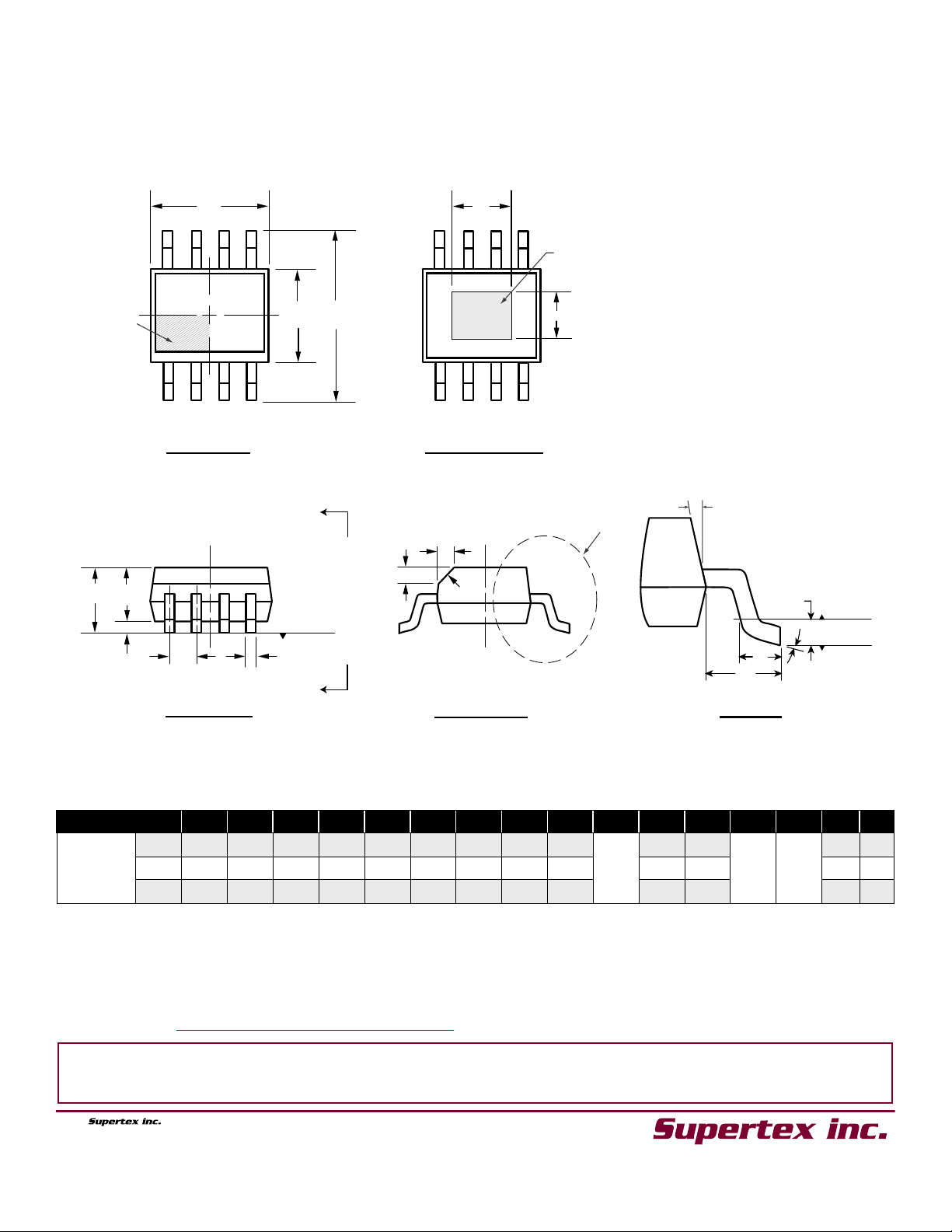
8-Lead SOIC (Narrow Body w/Heat Slug) Package Outline (SG)
4.90x3.90mm body, 1.70mm height (max), 1.27mm pitch
Notes:
Dimension
JEDEC Registration MS-012, Variation BA, Issue E, Sept. 2005.
* This dimension is not specified in the original JEDEC drawing. The value listed is for reference only.
† This dimension is a non-JEDEC dimension.
Drawings not to scale.
Supertex Doc. #: DSPD-8SOSG, Version C090408.
(The package drawing(s) in this data sheet may not reflect the most current specifications. For the latest package outline
information go to http://www.supertex.com/packaging.html.)
1.
This chamfer feature is optional. If it is not present, then a Pin 1 identifier must be located in the index area indicated. The Pin 1 Identifier can be:
a molded mark/identifier; an embedded metal marker; or a printed indicator.
Symbol A A1 A2 b D D1 E E1 E2 e h L L1 L2 θ θ1
MIN 1.25* 0.00 1.25 0.31 4.80*
(mm)
NOM - - - - 4.90 - 6.00 3.90 - - - - -
MAX 1.70 0.15 1.55* 0.51 5.00*
3.30
3.81
†
†
5.80* 3.80*
6.20* 4.00*
2.29
2.79
†
†
0.25 0.40
1.27
BSC
1.04
REF
0.50 1.27 8O15
0.25
BSC
Doc.# DSFP-HV9925
A091708
10
0O5
O
O
 Loading...