

Page 1
Supertex inc.
Supertex inc. ● 1235 Bordeaux Drive, Sunnyvale, CA 94089 ● Tel: 408-222-8888 ● www.supertex.com
Universal High Brightness
C
DD
R
T
R
CS
L1
Q1
D1
C
O
C
IN
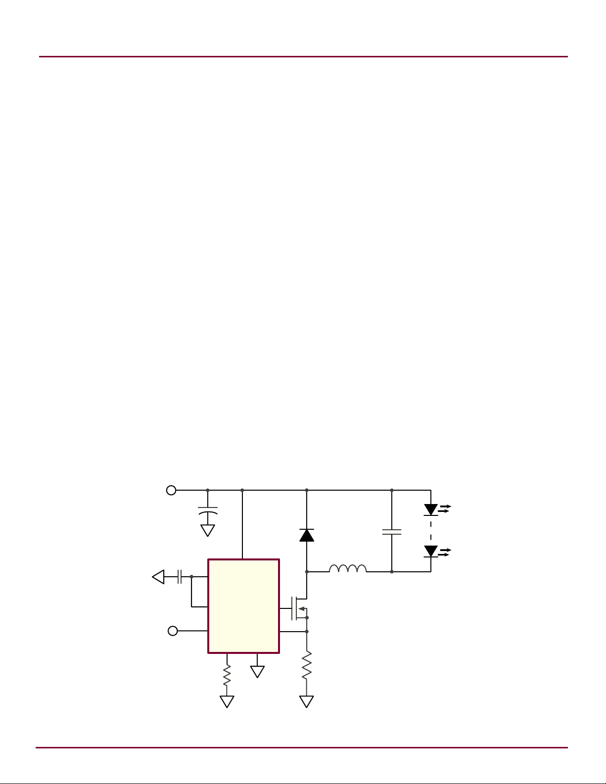
HV9910B
VIN
GATE
PWMD
VDD
LD
CS
RT
GN
D
LED Driver
HV9910B
Features
Switch mode controller for single switch LED drivers
►
Enhanced drop-in replacement to the HV9910
►
Open loop peak current controller
►
Internal 8.0 to 450V linear regulator
►
Constant frequency or constant off-time operation
►
Linear and PWM dimming capability
►
Requires few external components for operation
►
Applications
DC/DC or AC/DC LED driver applications
►
RGB backlighting LED driver
►
Back lighting of flat panel displays
►
General purpose constant current source
►
Signage and decorative LED lighting
►
Chargers
►
General Description
The HV9910B is an open loop, current mode, control LED
driver IC. The HV9910B can be programmed to operate in
either a constant frequency or constant off-time mode. It
includes an 8.0 - 450V linear regulator which allows it to work
from a wide range of input voltages without the need for an
external low voltage supply. The HV9910B includes a PWM
dimming input that can accept an external control signal with a
duty ratio of 0 - 100% and a frequency of up to a few kilohertz.
It also includes a 0 - 250mV linear dimming input which can
be used for linear dimming of the LED current.
The HV9910B is ideally suited for buck LED drivers. Since
the HV9910B operates in open loop current mode control, the
controller achieves good output current regulation without the
need for any loop compensation. PWM dimming response is
limited only by the rate of rise and fall of the inductor current,
enabling very fast rise and fall times. The HV9910B requires
only three external components (apart from the power stage)
to produce a controlled LED current making it an ideal solution
for low cost LED drivers.
Typical Application Circuit
Page 2
HV9910B
Supertex inc. ● 1235 Bordeaux Drive, Sunnyvale, CA 94089 ● Tel: 408-222-8888 ● www.supertex.com
1
2
3
4
5
6
7
8
16
15
14
13
12
11
10
9
8
7
6
5
1
2
3
4
VIN
CS
GND
GATE
RT
LD
VDD
PWM
D
VIN
NC
NC
CS
GND
NC
NC
GATE
NC
NC
RT
LD
VDD
NC
NC
PWM
D
Y = Last Digit of Year Sealed
WW = Week Sealed
L = Lot Number
= “Green” Packaging
YW W
9910B
LL LL
Y = Last Digit of Year Sealed
WW = Week Sealed
L = Lot Number
C = Country of Origin*
A = Assembler ID*
= “Green” Packaging
*May be part of top marking
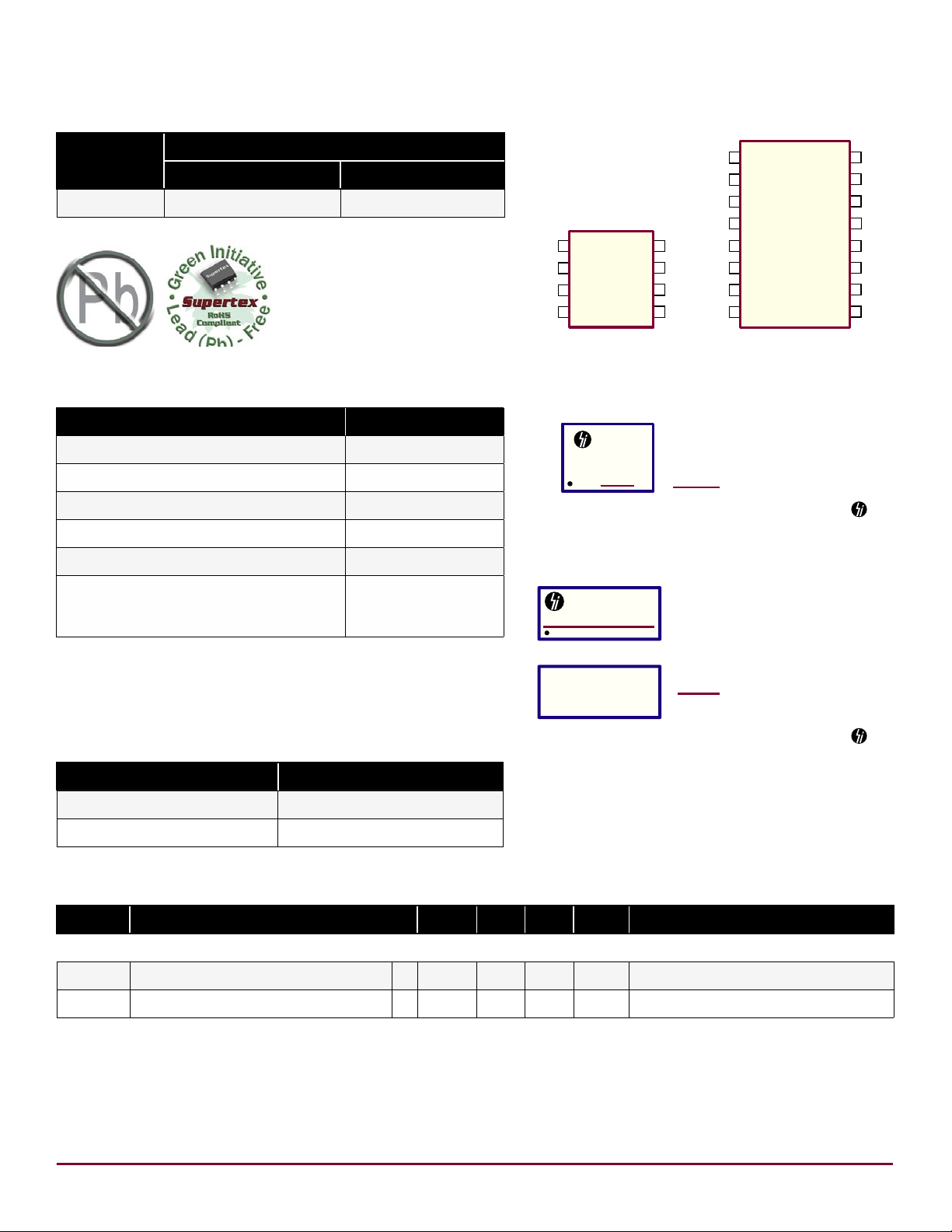
Top Marking
Bottom Marking
HV9910BNG
YWW LLLLLL LL
CCCCCCCCC AAA
Ordering Information
Device
8-Lead SOIC 16-Lead SOIC
HV9910B HV9910BLG-G HV9910BNG-G
-G indicates package is RoHS compliant (‘Green’)
Package Options
Absolute Maximum Ratings
Parameter Value
VIN to GND -0.5V to +470V
VDD to GND 12V
CS, LD, PWMD, GATE, RT to GND -0.3V to (V
Junction temperature range -40°C to +150°C
Storage temperature range -65°C to +150°C
Continuous power dissipation (T
= +25°C)
A
8-Lead SOIC
16-Lead SOIC
Stresses beyond those listed under “Absolute Maximum Ratings” may cause
permanent damage to the device. These are stress ratings only, and functional
operation of the device at these or any other conditions beyond those indicated in
the operational sections of the specifications is not implied. Exposure to absolute
maximum rating conditions for extended periods may affect device reliability.
+0.3V)
DD
630mW
1300mW
Pin Description
8-Lead SOIC (LG) 16-Lead SOIC (NG)
Product Marking
Package may or may not include the following marks: Si or
8-Lead SOIC (LG)
Thermal Resistance
Package θ
8-Lead SOIC 128OC/W
16-Lead SOIC 82OC/W
Electrical Characteristics (The specifications are at T
Sym Description Min Typ Max Units Conditions
Input
V
INDC
I
INSD
Notes:
1. Also limited by package power dissipation limit, whichever is lower.
† VDD load current external to the HV9910B.
* Denotes the specifications which apply over the full operating ambient temperature range of -40°C < TA < +125°C.
# Guaranteed by design.
Input DC supply voltage range
Shut-down mode supply current * - 0.5 1.0 mA Pin PWMD to GND
Package may or may not include the following marks: Si or
16-Lead SOIC (NG)
ja
= 25°C and V
A
1
* 8.0 - 450 V DC input voltage
2
= 12V, unless otherwise noted.)
IN
Page 3
HV9910B
Supertex inc. ● 1235 Bordeaux Drive, Sunnyvale, CA 94089 ● Tel: 408-222-8888 ● www.supertex.com
Electrical Characteristics (cont.) (The specifications are at T
= 25°C and V
A
= 12V, unless otherwise noted.)
IN
Sym Description Min Typ Max Units Conditions
Internal Regulator
V
= 8.0V, I
IN
GATE; RT = 226kΩ, PWMD = V
V
= 8.0 - 450V, I
IN
GATE; RT = 226kΩ, PWMD = V
ΔV
V
DD
DD, line
Internally regulated voltage - 7.25 7.5 7.75 V
Line regulation of V
DD
- 0 - 1.0 V
Internal Regulator
I
ΔV
DD, load
Load regulation of V
DD
- 0 - 100 mV
DD(ext)
RT = 226kΩ, PWMD = V
UVLO VDD undervoltage lockout threshold * 6.45 6.7 6.95 V VDD rising
∆UVLO VDD undervoltage lockout hysteresis - - 500 - mV VDD falling
I
IN,MAX
Current that the regulator can
supply before IC goes into UVLO
# 5.0 - - mA VIN = 8.0V
PWM Dimming
V
V
EN(lo)
EN(hi)
R
Pin PWMD input low voltage * - - 0.8 V VIN = 8.0 - 450V
Pin PWMD input high voltage * 2.0 - - V VIN = 8.0 - 450V
Pin PWMD pull-down resistance
EN
at PWMD
- 50 100 150 kΩ V
PWMD
(†)
= 0, 500pF at
DD(ext)
DD
= 0, 500pF at
DD(ext)
DD
= 0 - 1.0mA, 500pF at GATE;
DD
= 5.0V
Current Sense Comparator
V
V
OFFSET
T
t
DELAY
CS,TH
BLANK
Current sense pull-in threshold
voltage
225 250 275
-
mV
213 250 287 TA < +125°C
Offset voltage for LD comparator * -12 - 12 mV ---
- 150 215 280
Current sense blanking interval
- 145 215 315
Delay to output - - 80 150 ns
-40°C < T
< +85OC, VLD = VDD,
0 < T
A
VCS = V
ns
-40 < TA < +125OC, VLD = VDD,
VCS = V
VLD = VDD,
VCS = V
Oscillator
f
OSC
Oscillator frequency
- 20 25 30
kHz
- 80 100 120 RT = 226kΩ
RT = 1.00MΩ
GATE Driver
I
SOURCE
I
SINK
t
RISE
t
FALL
Notes:
1. Also limited by package power dissipation limit, whichever is lower.
† VDD load current external to the HV9910B.
* Denotes the specifications which apply over the full operating ambient temperature range of -40°C < TA < +125°C.
# Guaranteed by design.
GATE sourcing current - 165 - - mA V
GATE sinking current - 165 - - mA V
GATE output rise time - - 30 50 ns C
GATE output fall time - - 30 50 ns C
= 0V, V
GATE
= VDD, V
GATE
= 500pF, V
GATE
= 500pF, V
GATE
< +85°C
A
+ 50mV after T
CS,TH
+ 50mV after T
CS,TH
+ 50mV after T
CS,TH
= 7.5V
DD
= 7.5V
DD
DD
DD
BLANK
BLANK
BLANK
= 7.5V
= 7.5V
3
Page 4
Supertex inc. ● 1235 Bordeaux Drive, Sunnyvale, CA 94089 ● Tel: 408-222-8888 ● www.supertex.com
Application Information
The HV9910B is optimized to drive buck LED drivers using
open-loop peak current mode control. This method of control
enables fairly accurate LED current control without the need
for high side current sensing or the design of any closed loop
controllers. The IC uses very few external components and
enables both Linear and PWM dimming of the LED current.
A resistor connected to the RT pin programs the frequency
of operation (or the off-time). The oscillator produces pulses
at regular intervals. These pulses set the SR flip-flop in the
HV9910B which causes the GATE driver to turn on. The same
pulses also start the blanking timer which inhibits the reset
input of the SR flip flop and prevent false turn-offs due to the
turn-on spike. When the FET turns on, the current through
the inductor starts ramping up. This current flows through
the external sense resistor R
at the CS pin. The comparators are constantly comparing
the CS pin voltage to both the voltage at the LD pin and
the internal 250mV. Once the blanking timer is complete, the
output of these comparators is allowed to reset the flip flop.
When the output of either one of the two comparators goes
high, the flip flop is reset and the GATE output goes low. The
GATE goes low until the SR flip flop is set by the oscillator.
Assuming a 30% ripple in the inductor, the current sense
resistor RCS can be set using:
and produces a ramp voltage
CS
HV9910B
and any external resistor dividers needed to control the IC.
The VDD pin must be bypassed by a low ESR capacitor to
provide a low impedance path for the high frequency current
of the output GATE driver.
The HV9910B can also be operated by supplying a voltage
at the VDD pin greater than the internally regulated voltage.
This will turn off the internal linear regulator of the IC and the
HV9910B will operate directly off the voltage supplied at the
VDD pin. Please note that this external voltage at the VDD
pin should not exceed 12V.
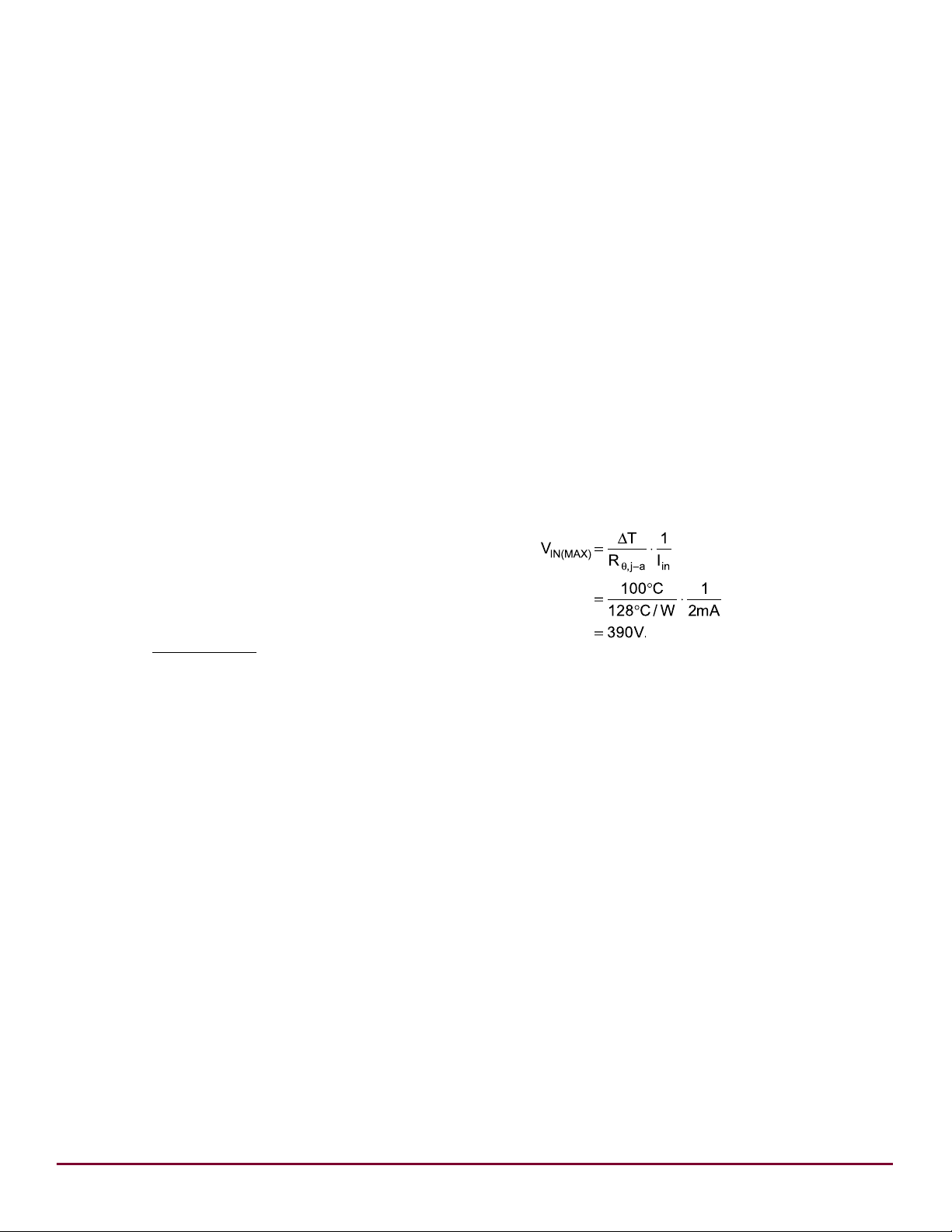
Although the VIN pin of the HV9910B is rated up to 450V,
the actual maximum voltage that can be applied is limited
by the power dissipation in the IC. For example, if an 8-pin
SOIC (junction to ambient thermal resistance R
W) HV9910B draws about I
= 2.0mA from the VIN pin, and
IN
has a maximum allowable temperature rise of the junction
temperature limited to about ΔT = 100°C, the maximum voltage at the VIN pin would be:
= 128°C/
θ,j-a
0.25V (or VLD)
R
CS
=
1.15 • I
LED
(A)
Constant frequency peak current mode control has an inherent disadvantage – at duty cycles greater than 0.5, the
control scheme goes into subharmonic oscillations. To prevent this, an artificial slope is typically added to the current
sense waveform. This slope compensation scheme will affect the accuracy of the LED current in the present form.
However, a constant off-time peak current control scheme
does not have this problem and can easily operate at duty
cycles greater then 0.5 and also gives inherent input voltage rejection making the LED current almost insensitive to
input voltage variations. But, it leads to variable frequency
operation and the frequency range depends greatly on the
input and output voltage variation. HV9910B makes it easy
to switch between the two modes of operation by changing
one connection (see oscillator section).
Input Voltage Regulator
The HV9910B can be powered directly from its VIN pin and
can work from 8.0 - 450VDC at its VIN pin. When a voltage
is applied at the VIN pin, the HV9910B maintains a constant
7.5V at the VDD pin. This voltage is used to power the IC
In these cases, to operate the HV9910B from higher input
voltages, a Zener diode can be added in series with the VIN
pin to divert some of the power loss from the HV9910B to
the Zener diode. In the above example, using a 100V zener
diode will allow the circuit to easily work up to 450V.
The input current drawn from the VIN pin is a sum of the
1.0mA current drawn by the internal circuit and the current
drawn by the GATE driver (which in turn depends on the
switching frequency and the GATE charge of the external
FET).
IIN ≈ 1.0mA + QG • fS
In the above equation, f
is the switching frequency and QG
S
is the GATE charge of the external FET (which can be obtained from the datasheet of the FET).
4
Page 5

HV9910B
Supertex inc. ● 1235 Bordeaux Drive, Sunnyvale, CA 94089 ● Tel: 408-222-8888 ● www.supertex.com
Current Sense
The current sense input of the HV9910B goes to the noninverting inputs of two comparators. The inverting terminal
of one comparator is tied to an internal 250mV reference
whereas the inverting terminal of the other comparator is
connected to the LD pin. The outputs of both these comparators are fed into an OR GATE and the output of the OR
GATE is fed into the reset pin of the flip-flop. Thus, the comparator which has the lowest voltage at the inverting terminal
determines when the GATE output is turned off.
The outputs of the comparators also include a 150-280ns
blanking time which prevents spurious turn-offs of the exter
nal FET due to the turn-on spike normally present in peak
current mode control. In rare cases, this internal blanking
might not be enough to filter out the turn-on spike. In these
cases, an external RC filter needs to be added between the
external sense resistor (RCS) and the CS pin.
Please note that the comparators are fast (with a typical
80ns response time). Hence these comparators are more
susceptible to be triggered by noise than the comparators
of the HV9910. A proper layout minimizing external induc
tances will prevent false triggering of these comparators.
Oscillator
The oscillator in the HV9910B is controlled by a single resistor connected at the RT pin. The equation governing the
oscillator time period t
is given by:
OSC
Linear Dimming
The Linear Dimming pin is used to control the LED current.
There are two cases when it may be necessary to use the
Linear Dimming pin.
► In some cases, it may not be possible to find the exact
RCS value required to obtain the LED current when the
internal 250mV is used. In these cases, an external voltage divider from the VDD pin can be connected to the LD
pin to obtain a voltage (less than 250mV) corresponding to
the desired voltage across RCS.
-
► Linear dimming may be desired to adjust the current
level to reduce the intensity of the LEDs. In these cases,
an external 0-250mV voltage can be connected to the LD
pin to adjust the LED current during operation.
To use the internal 250mV, the LD pin can be connected to
VDD.
Note:
Although the LD pin can be pulled to GND, the output cur-
-
rent will not go to zero. This is due to the presence of a minimum on-time (which is equal to the sum of the blanking time
and the delay to output time) which is about 450ns. This will
cause the FET to be on for a minimum of 450ns and thus the
LED current when LD = GND will not be zero. This current is
also dependent on the input voltage, inductance value, forward voltage of the LEDs and circuit parasitics. To get zero
LED current, the PWMD pin has to be used.
RT(kΩ) + 22
25
t
If the resistor is connected between RT and GND, HV9910B
operates in a constant frequency mode and the above equation determines the time-period. If the resistor is connected
between RT and GATE, the HV9910B operates in a constant
off-time mode and the above equation determines the offtime.
OSC
(μs) =
GATE Output
The GATE output of the HV9910B is used to drive an external FET. It is recommended that the GATE charge of the
external FET be less than 25nC for switching frequencies
≤100kHz and less than 15nC for switching frequencies >
100kHz.
PWM Dimming
PWM Dimming can be achieved by driving the PWMD pin
with a low frequency square wave signal. When the PWM
signal is zero, the GATE driver is turned off and when the
PWMD signal if high, the GATE driver is enabled. Since the
PWMD signal does not turn off the other parts of the IC,
the response of the HV9910B to the PWMD signal is almost
instantaneous. The rate of rise and fall of the LED current is
thus determined solely by the rise and fall times of the inductor current.
To disable PWM dimming and enable the HV9910B perma
nently, connect the PWMD pin to VDD.
-
5
Page 6
Supertex inc. ● 1235 Bordeaux Drive, Sunnyvale, CA 94089 ● Tel: 408-222-8888 ● www.supertex.com
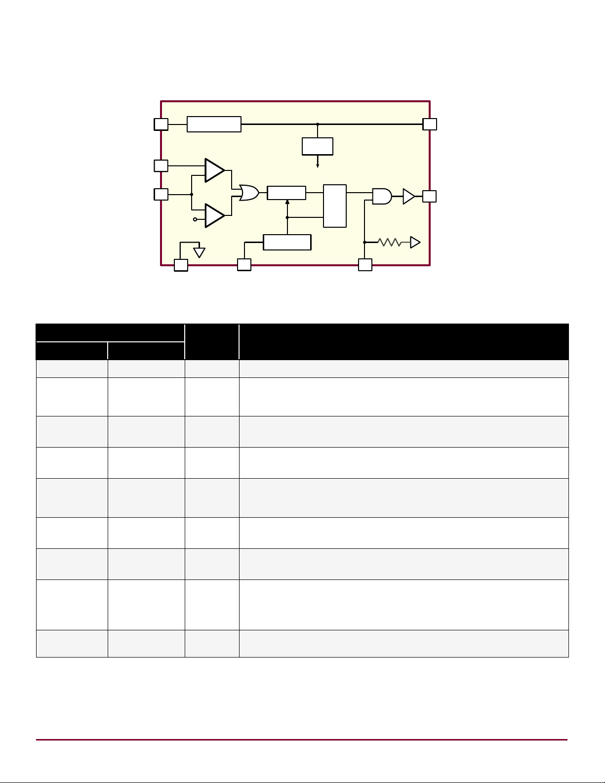
Block Diagram
POR
250mV
RT PWMD
GATE
VD
D
VI
N
LD
CS
GND
S
R
Q
Blanking
Oscillator
Regulator
+
-
+
-
Pin Description
HV9910B
Pin #
Function Description
8-Lead SOIC 16-Lead SOIC
1 1 VIN This pin is the input of an 8.0 - 450V linear regulator.
This pin is the current sense pin used to sense the FET current by means
2 4 CS
of an external sense resistor. When this pin exceeds the lower of either the
internal 250mV or the voltage at the LD pin, the GATE output goes low.
3 5 GND
4 8 GATE
Ground return for all internal circuitry. This pin must be electrically con
nected to the ground of the power train.
This pin is the output GATE driver for an external N-channel power
MOSFET.
This is the PWM dimming input of the IC. When this pin is pulled to GND,
5 9 PWMD
the GATE driver is turned off. When the pin is pulled high, the GATE driver
operates normally.
6 12 VDD
7 13 LD
This is the power supply pin for all internal circuits.
It must be bypassed with a low ESR capacitor to GND (≥0.1μF).
This pin is the linear dimming input and sets the current sense threshold as
long as the voltage at the pin is less than 250mV (typ).
This pin sets the oscillator frequency. When a resistor is connected be-
8 14 RT
tween RT and GND, the HV9910B operates in constant frequency mode.
When the resistor is connected between RT and GATE, the IC operates in
constant off-time mode.
-
2, 3, 6, 7, 10,
11, 15, 16
NC No connection
-
6
Page 7
Supertex inc. ● 1235 Bordeaux Drive, Sunnyvale, CA 94089 ● Tel: 408-222-8888 ● www.supertex.com
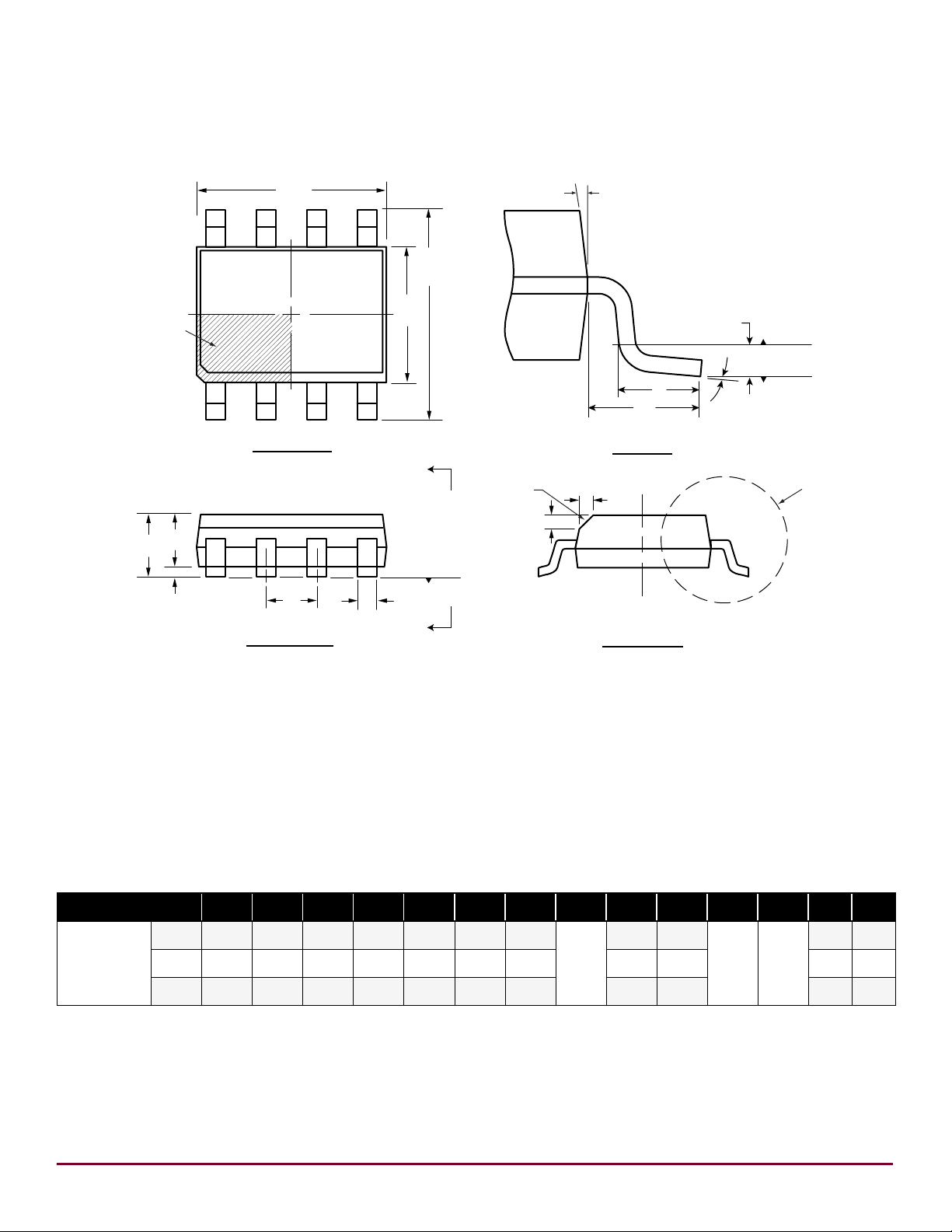
8-Lead SOIC (Narrow Body) Package Outline (LG)
1
8
Seating
Plane
Gauge
Plane
L
L1
L2
E
E1
D
e
b
A
A2
A1
Seating
Plane
A
A
Top View
Side View
View B
View B
θ1
θ
Note 1
(Index Area
D/2 x E1/2)
View A-A
h
h
Note 1
4.90x3.90mm body, 1.75mm height (max), 1.27mm pitch
HV9910B
Note:
This chamfer feature is optional. A Pin 1 identifier must be located in the index area indicated. The Pin 1 identifier can be: a molded mark/identifier;
1.
an embedded metal marker; or a printed indicator.
Symbol A A1 A2 b D E E1 e h L L1 L2 θ θ1
MIN 1.35* 0.10 1.25 0.31 4.80* 5.80* 3.80*
Dimension
(mm)
JEDEC Registration MS-012, Variation AA, Issue E, Sept. 2005.
* This dimension is not specified in the JEDEC drawing.
Drawings are not to scale.
Supertex Doc. #: DSPD-8SOLGTG, Version I041309.
NOM - - - - 4.90 6.00 3.90 - - - -
MAX 1.75 0.25 1.65* 0.51 5.00* 6.20* 4.00* 0.50 1.27 8
1.27
BSC
0.25 0.40
1.04
REF
0.25
BSC
7
O
0
O
5
O
15
O
Page 8
Supertex inc. does not recommend the use of its products in life support applications, and will not knowingly sell them for use in such applications unless it receives
an adequate “product liability indemnification insurance agreement.”
Supertex inc. does not assume responsibility for use of devices described, and limits its liability
to the replacement of the devices determined defective due to workmanship. No responsibility is assumed for possible omissions and inaccuracies. Circuitry an
d
specifications are subject to change without notice. For the latest product specifications refer to the
Supertex inc. (website: http//www.supertex.com)
©2010 Supertex inc. All rights reserved. Unauthorized use or reproduction is prohibited.
Supertex inc.
1235 Bordeaux Drive, Sunnyvale, CA 94089
Tel: 408-222-8888
www.supertex.com
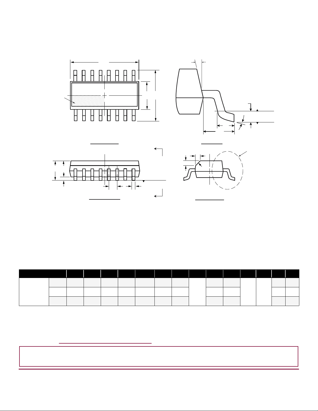
16-Lead SOIC (Narrow Body) Package Outline (NG)
D
Seating
Plane
Gauge
Plane
L
L1
L2
Top View
Side View
View A-A
View B
View
B
θ1
θ
E1
E
A
A2
A1
A
A
Seating
Plane
e
b
h
h
16
1
Note 1
Note 1
(Index Area
D/2 x E1/2)
9.90x3.90mm body, 1.75mm height (max), 1.27mm pitch
HV9910B
Note:
This chamfer feature is optional. If it is not present, then a Pin 1 identifier must be located in the index area indicated. The Pin 1 identifier can be:
1.
a molded mark/identifier; an embedded metal marker; or a printed indicator.
Symbol A A1 A2 b D E E1 e h L L1 L2 θ θ1
Dimension
(mm)
JEDEC Registration MS-012, Variation AC, Issue E, Sept. 2005.
* This dimension is not specified in the JEDEC drawing.
Drawings are not to scale.
Supertex Doc. #: DSPD-16SONG, Version G041309.
MIN 1.35* 0.10 1.25 0.31 9.80* 5.80* 3.80*
NOM - - - - 9.90 6.00 3.90 - - - -
MAX 1.75 0.25 1.65* 0.51 10.00* 6.20* 4.00* 0.50 1.27 8O15
(The package drawing(s) in this data sheet may not reflect the most current specifications. For the latest package outline
1.27
BSC
0.25 0.40
1.04
0.25
REF
BSC
information go to http://www.supertex.com/packaging.html.)
Doc.# DSFP-HV9910B
B061209
8
O
0
O
5
O
Page 9
Supertex inc.
Supertex inc. ● 1235 Bordeaux Drive, Sunnyvale, CA 94089 ● Tel: 408-222-8888 ● www.supertex.com
Off-Line, High Brightness, 1.4A
90 - 135VAC
50/60Hz
10 - 40V, 1.4A max.
LED Driver Demo Board
HV9910BDB1
General Description
The HV9910BDB1 demoboard is an offline, high current
LED driver designed to drive a 40V LED string at 1.4A from
a 110V input. The demoboard uses Supertex’s HV9910B
LED driver IC to drive a buck converter.
The HV9910BDB1 has a typical full load efficiency of 88%,
with the buck converter efficiency (excluding the diode
bridge rectifier and EMI filter) at 93%. The demoboard also
meets CISPR-15 conducted EMI standards.
The output current can be adjusted in two ways - either
with linear dimming using the onboard potentiometer or
with PWM dimming by applying a TTL-compatible square
wave signal at the PWMD terminal. Using linear dimming,
the output current of the HV9910DB1 can be lowered to
about 0.1A (note: zero output current can be obtained only
by PWM dimming).
Specifications
Input voltage 90 - 135Vrms, 50/60Hz
Output voltage 10 - 40V
Output current 1.4A max
Output current ripple (typ) 40% (peak-peak)
Full load efficiency (@110V)
Power factor (@110V)
Input current (@110V) 0.83A rms
Input current THD (@110V) 117%
Switching frequency (typ) 50kHz
Minimum output current (@110V)
Conducted EMI Meets CISPR-15
Temperature rise of heatsink
(@110V input and full load)
Open LED protection yes
Output short circuit protection no
Dimensions 86.4mm X 58.4mm
88%
0.64
0.1A
50°C
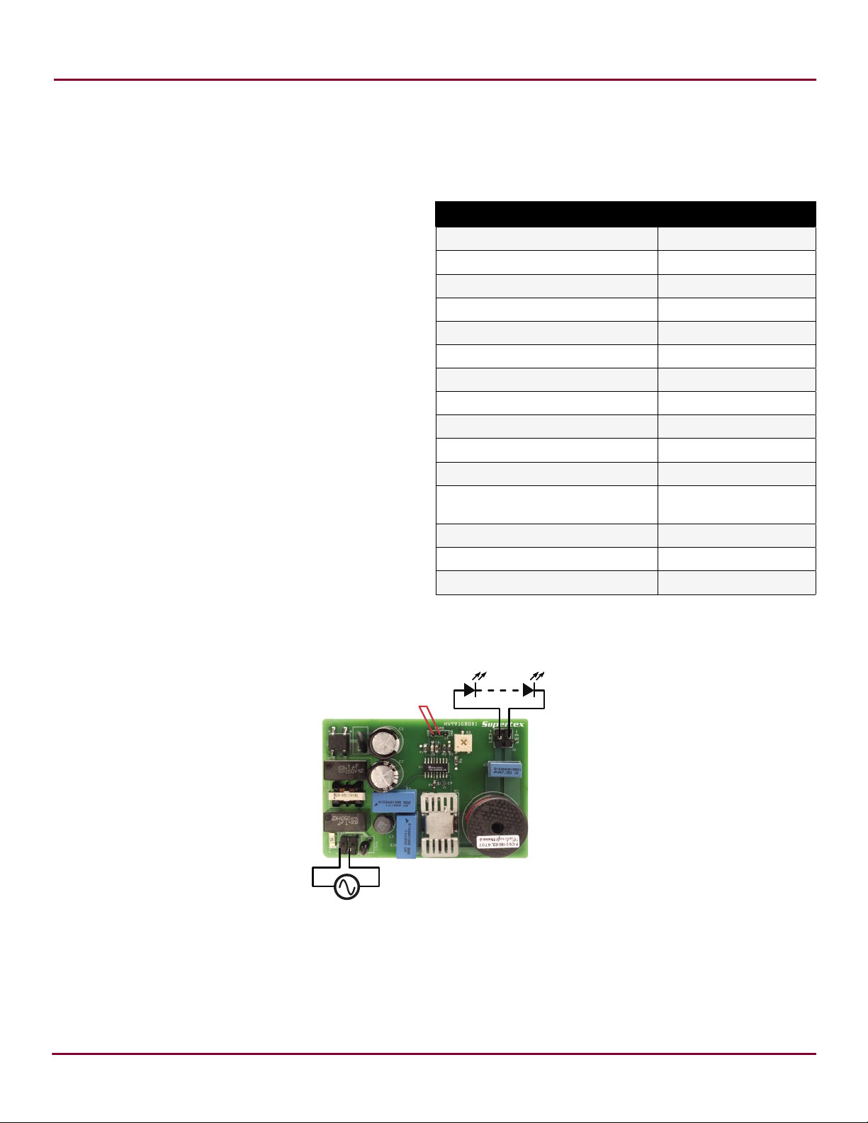
Connection Diagram
WARNING!!!
Do not connect earth-grounded test instruments. Doing so will short the AC line, resulting in damage to the
instrument and/or the HV9910BDB1. Use floating high voltage differential probes or isolate the demoboard
by using an isolating transformer.
There is no galvanic isolation. Dangerous voltages are present when connected to the AC line.
1
Page 10
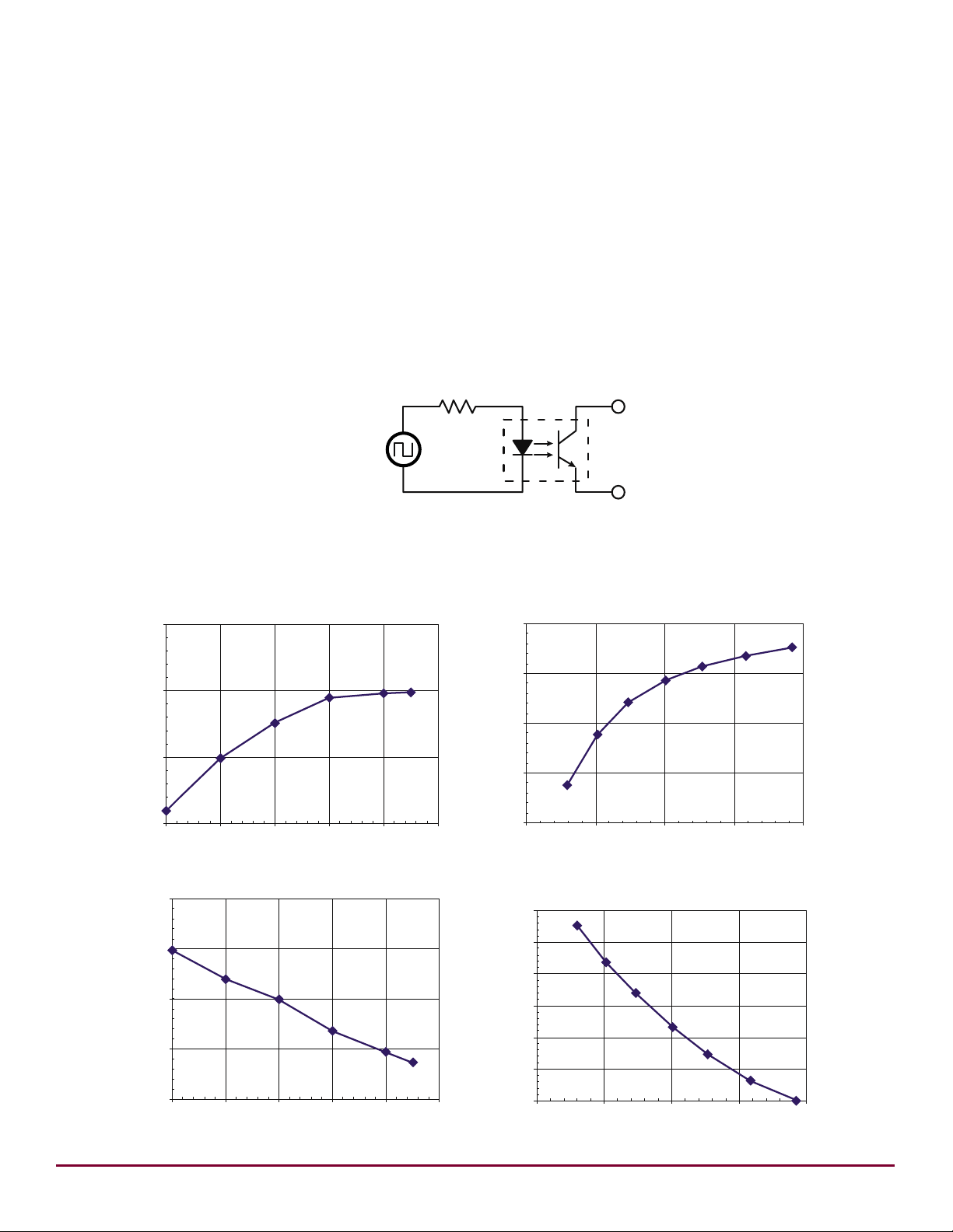
HV9910BDB1
Supertex inc. ● 1235 Bordeaux Drive, Sunnyvale, CA 94089 ● Tel: 408-222-8888 ● www.supertex.com
VDD
PWMD
Opto-isolator
(eg: LTV-814 from Lite-On)
5.0V
square wave signal
(<1.0kHz)
3.8kΩ
Full Load Efficiency vs. Input Voltage
86
87
88
89
90 100 110 120 130 140
Input Voltage (Vrms)
Efficiency (%)
Efficiency vs. Load Voltage (@VIN=110V rms)
74
78
82
86
90
5 15 25 35 4
5
Load Voltage (V
)
Efficiency (%)
Load Regulation of Load Current
(@
V
IN
= 110V rms)
0
2.5
5
7.5
10
12.5
15
5 15 25 35 4
5
Load Voltage (V)
Change in output current (%)
Line Regulation of Load Current
-5
-2.5
0
2.5
5
90 100 110 120 130 140
Input Voltage (Vrms)
Change in output current (%)
Connections
1. Connect the input AC voltage between the AC IN terminals as shown in the connection diagram.
2. Connect the LED string between LED+ (anode of LED string) and LED- (cathode of LED string).
3. Connect the PWMD terminal to the VDD terminal using the jumper provided to enable the LED driver.
4. The current level can be adjusted using the on-board potentiometer.
PWM Dimming
The HV9910BDB1 is capable of being PWM dimmed by applying a square wave TTL compatible signal between PWMD
and GND terminals. However, since there is no galvanic isolation on the board, care must be taken to prevent damage to
the PWM dimming source and/or the HV9910BDB1. One simple way is to isolate the LED driver from the AC line using an
isolation transformer. Another approach is to use an opto-isolator to drive the PWMD pin as shown in the figure below.
Typical Results
2
Page 11
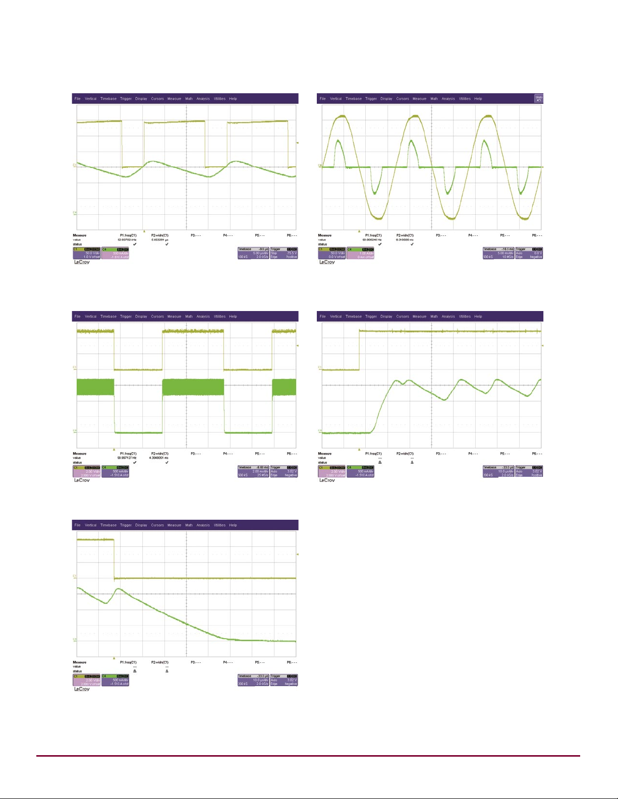
Supertex inc. ● 1235 Bordeaux Drive, Sunnyvale, CA 94089 ● Tel: 408-222-8888 ● www.supertex.com
Waveforms
Steady State waveforms at 150Vdc input and full
load output
LED Current
Drain Voltag
e
PWM Dimming at 100Hz
LED Curren
t
PWMD Voltag
e
Steady State waveforms at 150Vdc input and full
load output
Input Voltage
Input
Curren
t
Rising Edge of LED Current during PWM Dimming
LED Curren
t
PWMD Voltag
e
Falling Edge of LED Current during PWM Dimming
LED Curren
t
PWMD Voltage
HV9910BDB1
3
Page 12
Supertex inc. ● 1235 Bordeaux Drive, Sunnyvale, CA 94089 ● Tel: 408-222-8888 ● www.supertex.com
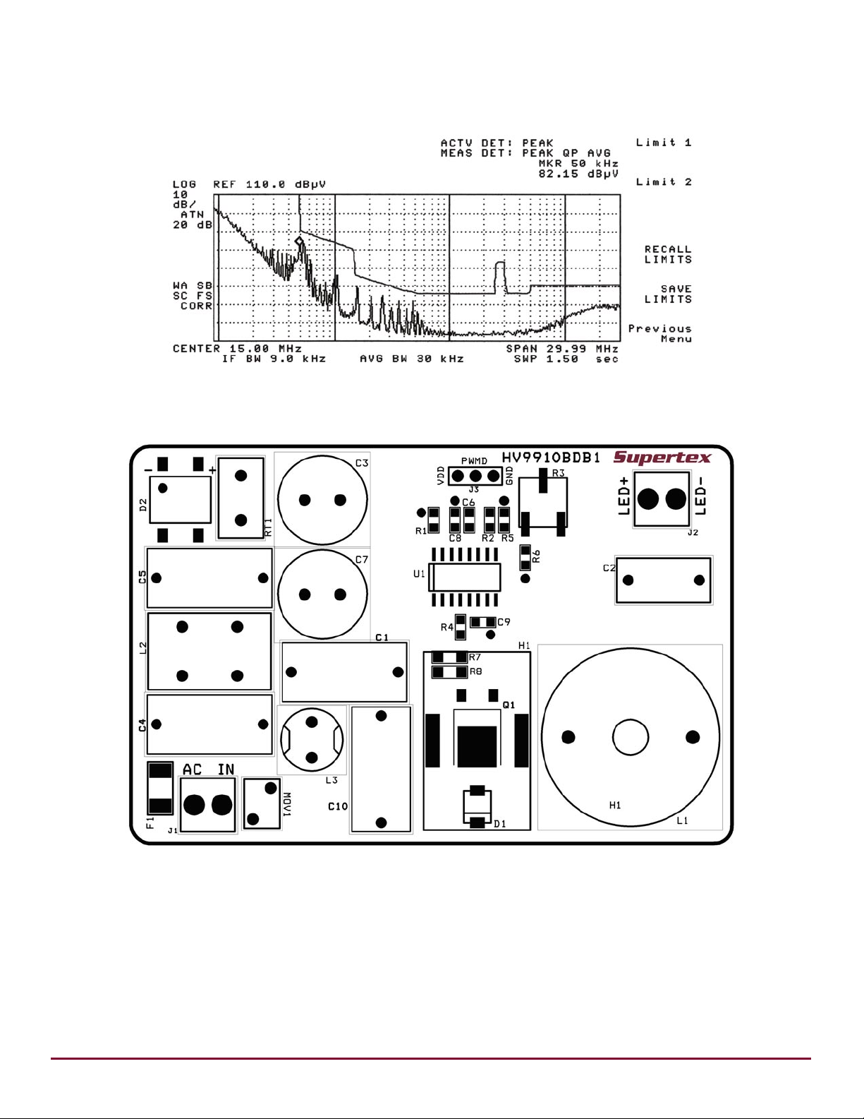
Conducted EMI Measurements at Full Load and 110V AC input
CISPR-15 Limit
Silk Screen
HV9910BDB1
4
Page 13
Supertex inc. ● 1235 Bordeaux Drive, Sunnyvale, CA 94089 ● Tel: 408-222-8888 ● www.supertex.com
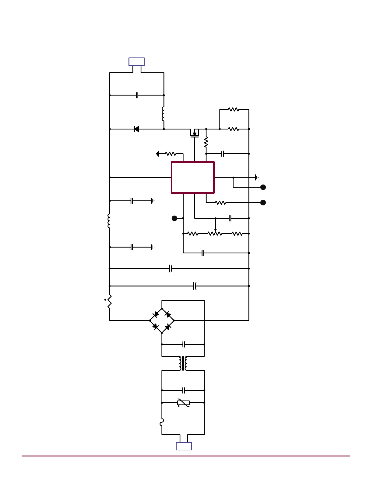
Schematic Diagram
t
RT1
CL
-
13
0
0
1
2
L1
1000
µH
2A
0
1
4
3
2
-
+
D2
DF1
5
04S-
T
R4
0.
0
D1
MURS240
Q1
FQD8N
2
5
1
2
1
2
J1
1
2
4
3
L2
R5
1k
F1
2A
125V
1
C4
0.1µ
F
250
V
4
MOV1
R
ERZ-V05D221
1
2
J2
1
J3
A
2
3
1
LD
13
PW
M
D
9
5
CS
4
GATE
8
RT
14
VIN
12
HV99
10B
U1
C5
0.1µ
F
250
V
C1
1.0µF
250
V
0
C10
1.0µ
F
250
V
C2
0.47µF
250
V
C6
2.2µ
F
16V
R7
0.27
0.25
W
R7
0.27
0.25
W
C1
1.0µ
F
250
V
J3
C
J3
B
C8
0.1µ
F
16V
R6
1k
R2
178k
R3
5k
R1
464k
L3
22
µH
C3
68µ
F
200
V
C7
68µ
F
200
V
VDD
GND
HV9910BDB1
5
Page 14

Supertex inc. does not recommend the use of its products in life support applications, and will not knowingly sell them for use in such applications unless it receives
an adequate “product liability indemnification insurance agreement.”
Supertex inc. does not assume responsibility for use of devices described, and limits its liability
to the replacement of the devices determined defective due to workmanship. No responsibility is assumed for possible omissions and inaccuracies. Circuitry an
d
specifications are subject to change without notice. For the latest product specifications refer to the
Supertex inc. (website: http//www.supertex.com)
©2010 Supertex inc. All rights reserved. Unauthorized use or reproduction is prohibited.
Supertex inc.
1235 Bordeaux Drive, Sunnyvale, CA 94089
Tel: 408-222-8888
www.supertex.com
Bill of Materials
HV9910BDB1
Item
#
Qty RefDes Description Package Manufacturer
Manufacturer’s Part
Number
1 2 C1, C10 1µF, 250V metallized polyester capacitor Radial EPCOS Inc B32522C3105J
2 1 C2
0.47µF, 250V metallized polyester ca
pacitor
Radial EPCOS Inc B32521C3474J
3 2 C3, C7 68µF, 250V electrolytic capacitor Radial Panasonic EEU-EE2D680
4 2 C4, C5
0.1µF, 250V metallized polyester X2
capacitor
Radial Panasonic ECQ-U2A104MV
5 1 C6 2.2µF, 16V, X7R ceramic chip capacitor SMD0805 --- ---
6 1 C8 0.1µF, 50V, X7R ceramic chip capacitor SMD0805 --- ---
7 1 C9 open --- --- ---
8 1 D1 400V, 2A ultra fast recovery diode SMB ON Semi MURS240T3
9 1 D2 400V, 1.5A single phase diode bridge DF-S Diodes Inc DF1504S-T
10 1 F1 2A, 125V slow blow fuse SMT Littelfuse Inc 0452002.MRL
11 2 J1, J2 2 position 0.156” header Thru-Hole Molex 26-48-1021
12 1 J3 3 position, 0.1” pitch vertical header Thru-Hole Molex 22-28-4030
13 1 L1 1000µH, 2A rms, 2A sat inductor Radial Coilcraft PCV-2-105-02L
- - --- Cross Reference Radial Coiltronics CTX01-17784G-R
14 1 L2 0.6mH, 1A rms common mode choke Thru-Hole Coilcraft BU9-6011R0BL
15 1 L3 22µH, 2.1A sat, 1.9A rms inductor Radial Coilcraft RFB0807-220L
16 1 MOV1 220V, 600A surge absorber Radial Panasonic ERZ-V05D221
17 1 Q1 250V, 0.55Ω, N-channel FET DPAK Fairchild Semi FQD8N25
18 1 RT1 2A rms, 50Ω inrush current limiter Radial GE Sensing CL-130
19 1 R1 464KΩ, 1/8W, 1% chip resistor SMD0805 --- ---
20 1 R2 178KΩ, 1/8W, 1% chip resistor SMD0805 --- ---
21 1 R3 5KΩ 6mmsq single turn potentiometer SMT Bourns Inc 3361P-1-502GLF
22 1 R4 0.0Ω, 1/8W chip resistor SMD0805 --- ---
23 2 R5, R6 1KΩ, 1/8W, 1% chip resistor SMD0805 --- ---
24 2 R7, R8 0.27Ω, 1/4W, 1% chip resistor SMD1206 --- ---
25 1 U1 Universal LED Driver SO-16 Supertex HV9910BNG-G
100410
6
Page 15
● 1235 Bordeaux Drive, Sunnyvale, CA 94089 ● Tel: 408-222-8888 ● www.supertex.com
90 - 265VAC
50/60Hz
10 - 40V,
350mA max.
Universal, Off-Line, High Brightness,
350mA LED Driver Demo Board
HV9910BDB2
General Description
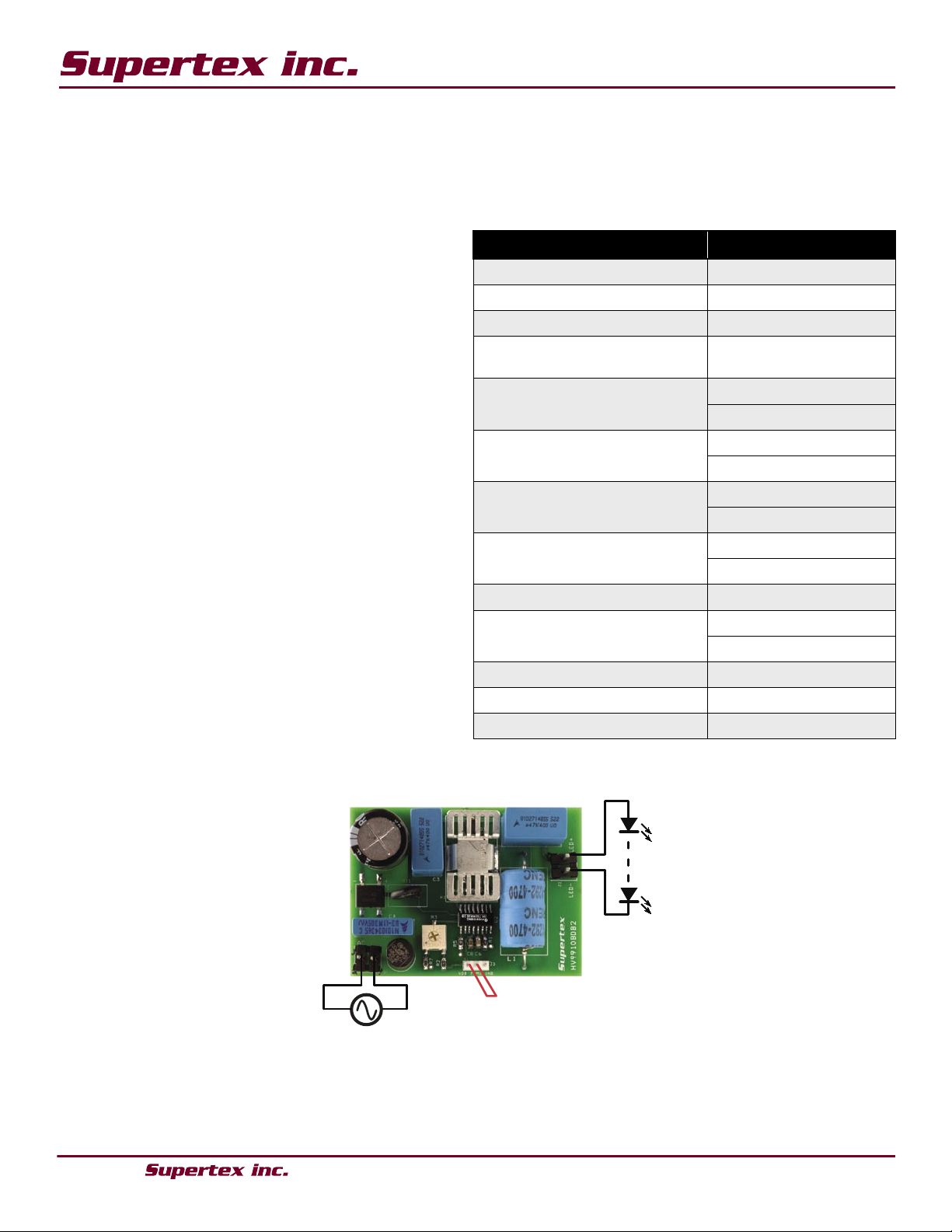
The Supertex HV9910BDB2 demo board is a HighBrightness LED power driver to supply a string of LEDs
using the HV9910B IC from a universal AC input voltage.
The HV9910BDB2 can supply a maximum output current
of 350mA to drive 10 - 40V LED strings from a wide input
voltage - 90 to 265VAC, 50/60Hz.
The power conversion stage of the HV9910BDB2 consists
of a diode bridge rectifier followed by a current-controlled
buck converter operating at a switching frequency of
50kHz. The nominal output current of the demo board can
be adjusted to any value between 30 and 350mA using
the on-board trimming potentiometer. PWM dimming can
be achieved by applying a pulse-width-modulated square
wave signal between the PWMD and GND pins. Zero
output current can be obtained only by PWM dimming.
The HV9910BDB2 is not CISPR-15 compliant. Additional
filtering is required to make the board meet CISPR-15
limits.
Specifications
Parameter Value
Input voltage 90 - 265Vrms, 50/60Hz
Output voltage 10 - 40V
Output current 350mA max
Output current ripple (typ)
@110V input
Full load efficiency
Power factor
Input current (rms)
Input current THD
Switching frequency (typ) 50kHz
Minimum output current
Open LED protection yes
Output short circuit protection no
Dimensions 68.6mm X 49.6mm
25% (peak-peak)
@40V output, 350mA
88% @110VAC
86% @230VAC
0.70 @110VAC
0.48 @230VAC
0.20A @110VAC
0.14A @230VAC
94% @110VAC
95% @230VAC
20mA @110VAC
30mA @230VAC
Connection Diagram
WARNING!!!
Do not connect earth-grounded test instruments. Doing so will short the AC line, resulting in damage to the instrument and/or
the HV9910BDB2. Use floating high voltage differential probes or isolate the demoboard by using an isolating transformer.
There is no galvanic isolation. Dangerous voltages are present when connected to the AC line.
1
Page 16
HV9910BDB2
● 1235 Bordeaux Drive, Sunnyvale, CA 94089 ● Tel: 408-222-8888 ● www.supertex.com
VDD
PWMD
Opto-isolator
(eg: LTV-814 from Lite-On)
5.0V
square wave signal
(<1.0kHz)
3.8kΩ
Efficiency vs.Input Voltage
60
65
70
75
80
85
90
80 130 180 230 280
Input Voltage (VAC)
Efficiency (%)
40V output
10V output
Efficiency vs. LED String Voltage
60
65
70
75
80
85
90
0 10 20 30 40 5
0
LED String Voltage (V
)
Efficiency (%)
110VAC Input
230VAC Input
Current Regulation vs. Input Voltage
-10
-5
0
5
10
80 130 180 230 280
Input Voltage (VAC)
% change in LED Current
40V Ouput
10V Output
Current Regulation vs. LED String
Voltag
e
0
5
10
15
20
0 10 20 30 40 5
0
LED String Voltage (V
)
% change in LED Current
110VAC Input
230VAC Input
Connections
Connect the input AC voltage between the AC IN
1.
terminals as shown in the connection diagram.
Connect the LED string between LED+ (anode of LED
2.
string) and LED- (cathode of LED string).
Connect the PWMD terminal to the VDD terminal using
3.
the jumper provided to enable the LED driver.
The current level can be adjusted using the on-board
4.
potentiometer.
PWM Dimming
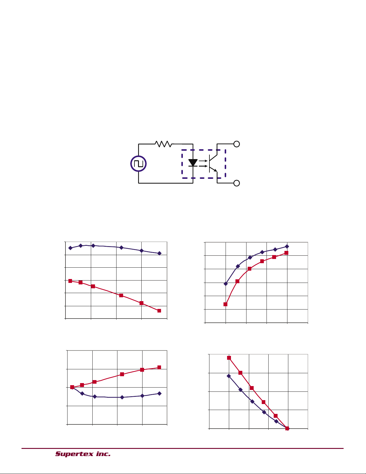
The HV9910BDB2 is capable of being PWM dimmed by
applying a square wave TTL compatible signal between
PWMD and GND terminals. However, since there is no
galvanic isolation on the board, care must be taken to
prevent damage to the PWM dimming source and/or the
HV9910BDB2. One simple way is to isolate the LED driver
from the AC line using an isolation transformer. Another
approach is to use an opto-isolator to drive the PWMD pin
as shown in the figure below.
Typical Results
2
Page 17
● 1235 Bordeaux Drive, Sunnyvale, CA 94089 ● Tel: 408-222-8888 ● www.supertex.com
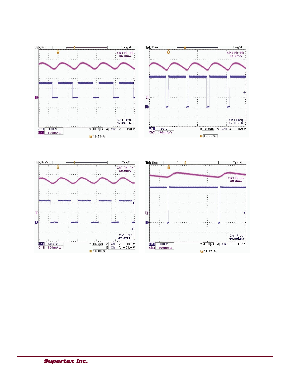
Waveforms
Steady State waveforms at 110VAC input and full
load output
LED Current
Drain Voltage
Steady State waveforms at 230VAC input and full
load output
LED Current
Drain Voltage
Steady State waveforms at 90VAC input and
40V, 350mA output
LED Current
Drain Voltage
Steady State waveforms at 230VAC input and
10V, 350mA output
LED Current
Drain Voltage
HV9910BDB2
3
Page 18
● 1235 Bordeaux Drive, Sunnyvale, CA 94089 ● Tel: 408-222-8888 ● www.supertex.com
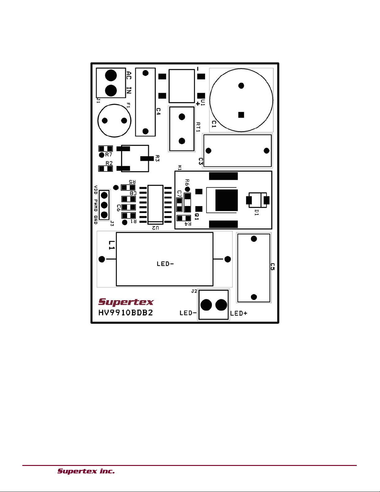
Silk Screen
HV9910BDB2
4
Page 19
● 1235 Bordeaux Drive, Sunnyvale, CA 94089 ● Tel: 408-222-8888 ● www.supertex.com
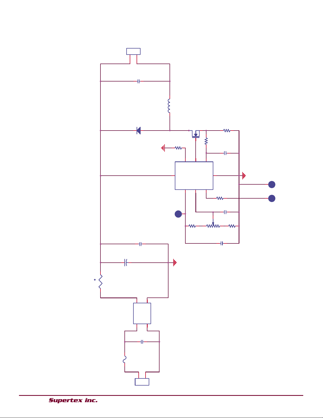
Schematic Diagram
t
R
T
1
C
L
-
1
4
0
C
4
0.1uF, 305VAC
1
2
L
1
4
.
7
m
H
C
3
0.47uF, 400V
R
1
4
6
4
K
R
6
0
.
5
6
C
1
22uF, 400V
D
1
S
T
T
H
2
R
0
6
U
Vin
1
H
D
1
3
E
N
9
Gnd
5
C
S
4
G
a
t
e
8
R
o
s
c
1
4
V
d
d
1
2
H
V
9
9
1
0
U
2
1
2
J
2
1
2
J
1
F
1
2
A
,
2
5
0
VA
C
R
2
1
7
8
K
R
7
1
K
C
6
0.1uF
C
8
2.2uF, 16V
R
5
1
k
1
J
3
A
R
3
5
K
R
L
-
1
2
9
2
-
4
7
0
0
C
5
0.47uF, 400V
A
C
1
A
C
2
P
O
S
N
E
G
U
1
2
J
3
B
3
J
3
C
Q
1
S
T
D
7
N
M
5
0
N
R
4
1
k
C
7
1
0
0
p
F
HV9910BDB2
5
Page 20
Supertex inc. does not recommend the use of its products in life support applications, and will not knowingly sell them for use in such applications unless it receives an
adequate “product liability indemnification insurance agreement.” Supertex inc. does not assume responsibility for use of devices described, and limits its liability to the
replacement of the devices determined defective due to workmanship. No responsibility is assumed for possible omissions and inaccuracies. Circuitry and specifications
are subject to change without notice. For the latest product specifications refer to the Supertex inc. website: http//www.supertex.com
.
©2009 All rights reserved. Unauthorized use or reproduction is prohibited .
1235 Bordeaux Drive, Sunnyvale, CA 94089
Tel: 408-222-8888
www.supertex.com
HV9910BDB2
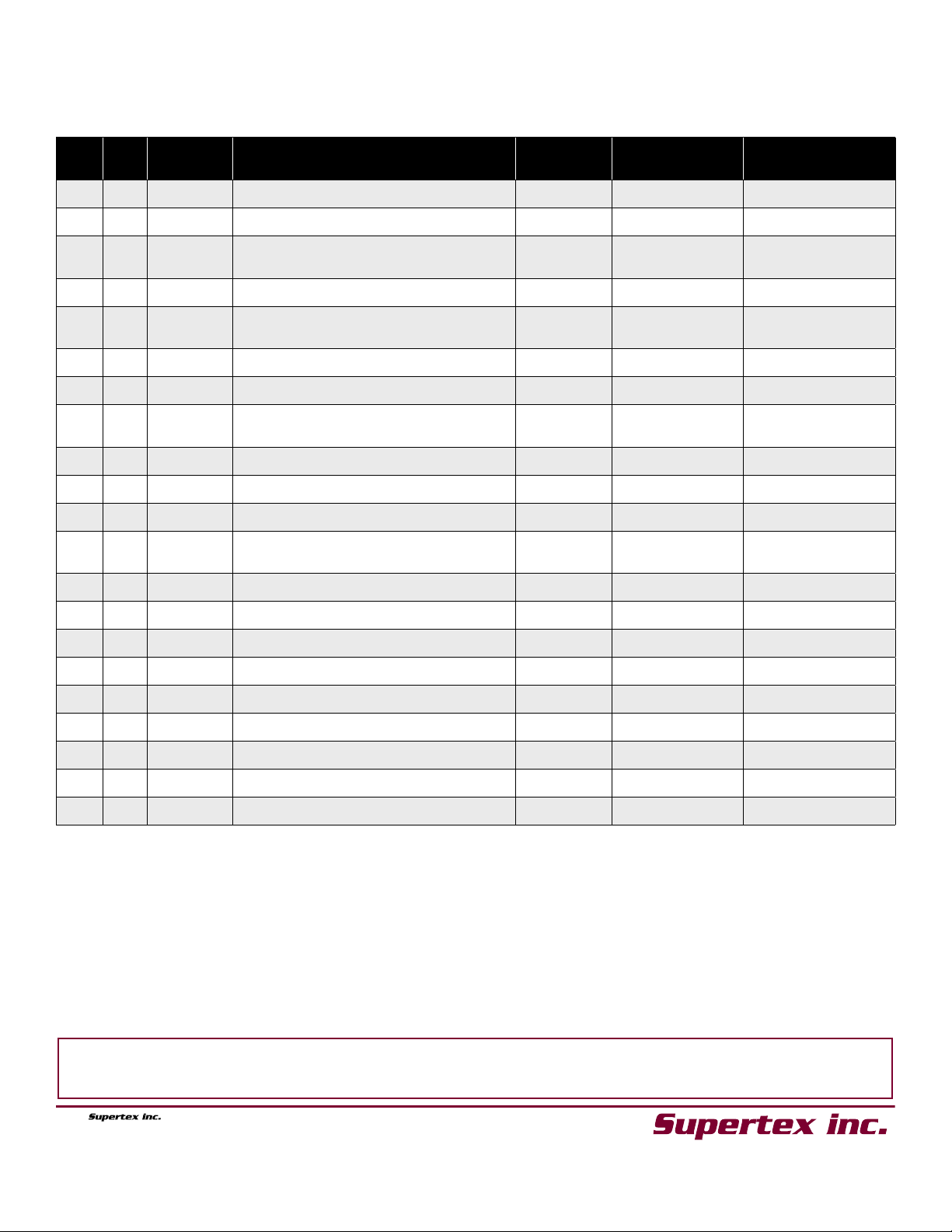
Bill of Materials
Item
Qty RefDes Description Package Manufacturer
#
1 1 C1 22µF, 400V electrolytic capacitor Radial Nichion UVR2G220MHD
2 2 C3,C5 0.47µF, 400V metal film capacitor Radial EPCOS Inc B32522C6474K
3 1 C4
0.1µF, 305VAC EMI suppresion
capacitor
Radial EPCOS Inc B32922C3104M
4 1 C6 0.1µF, 16V X7R ceramic chip capacitor SMD0805 Panasonic ECJ-2VB1C104K
5 1 C7
100pF, 50V C0G ceramic chip
capacitor
SMD0805 TDK Corp C2012C0G1H101J
6 1 C8 2.2µF, 16V X7R ceramic chip capacitor SMD0805 TDK Corp C2012X7R1C225K
7 1 D1 600V, 2A ultrafast diode SMB ST Micro STTH2R06U
8 1 F1 2A, 250VAC time lag fuse Radial
Cooper
Bussman
9 1 H1 15C/W DPAK heatsink SMT Aavid 7106PD
10 2 J1,J2 2 position, 0.156” pitch, vertical header Thru-Hole Molex 26-48-1021
11 1 J3 3 position, 0.100” pitch, vertical header Thru-Hole Molex 22-03-2031
12 1 L1
4.7mH, 400mA rms,
470mA sat inductor
Axial Renco USA RL-1292-4700
13 1 Q1 550V, 0.7Ω N-channel FET DPAK ST Micro STD5NM50
Manufacturer’s
Part Number
SR-5-2A-BK
14 1 RT1 50Ω NTC inrush limiter Thru-Hole GE Sensing CL-140
15 1 R1 464KΩ, 1/8W, 1% chip resistor SMD0805 --- ---
16 1 R2 178KΩ, 1/8W, 1% chip resistor SMD0805 --- ---
17 1 R3 5KΩ top adjust trimpot SMT Bourns Inc 3361P-1-502G
18 3 R4,R5,R7 1KΩ, 1/8W, 1% chip resistor SMD0805 --- ---
19 1 R6 0.56Ω, 1/4W, 1% chip resistor SMD1206 --- ---
20 1 U1 400V, 1A single phase diode bridge DF-S Diodes Inc DF04S
21 1 U2 Universal LED Driver SO-16 Supertex HV9910BNG-G
012309
6
Page 21
● 1235 Bordeaux Drive, Sunnyvale, CA 94089 ● Tel: 408-222-8888 ● www.supertex.com
HV9910BDB3
+
Short for
constant frequency mode
+
-
Short for
constant off-time mode
Low Voltage, High Current, LED Driver Demoboard
General Description
The HV9910BDB3 demoboard is a high current LED driver
designed to drive one LED or two LEDs in series at currents
up to 1.0A from a 10 – 30V DC input. The demoboard uses
Supertex’s HV9910B Universal LED driver IC to drive a
buck converter.
The HV9910BDB3 can be configured to operate in either a
constant frequency mode (for driving a single LED) or in a
constant off-time mode (for driving two LEDs).
The output current can be adjusted in two ways – either
with linear dimming using the onboard potentiometer or
with PWM dimming by applying a TTL – compatible square
wave signal at the PWMD terminal. Using linear dimming,
the output current of the HV9910DB1 can be lowered to
about 0.01A (note: zero output current can be obtained
only by PWM dimming).
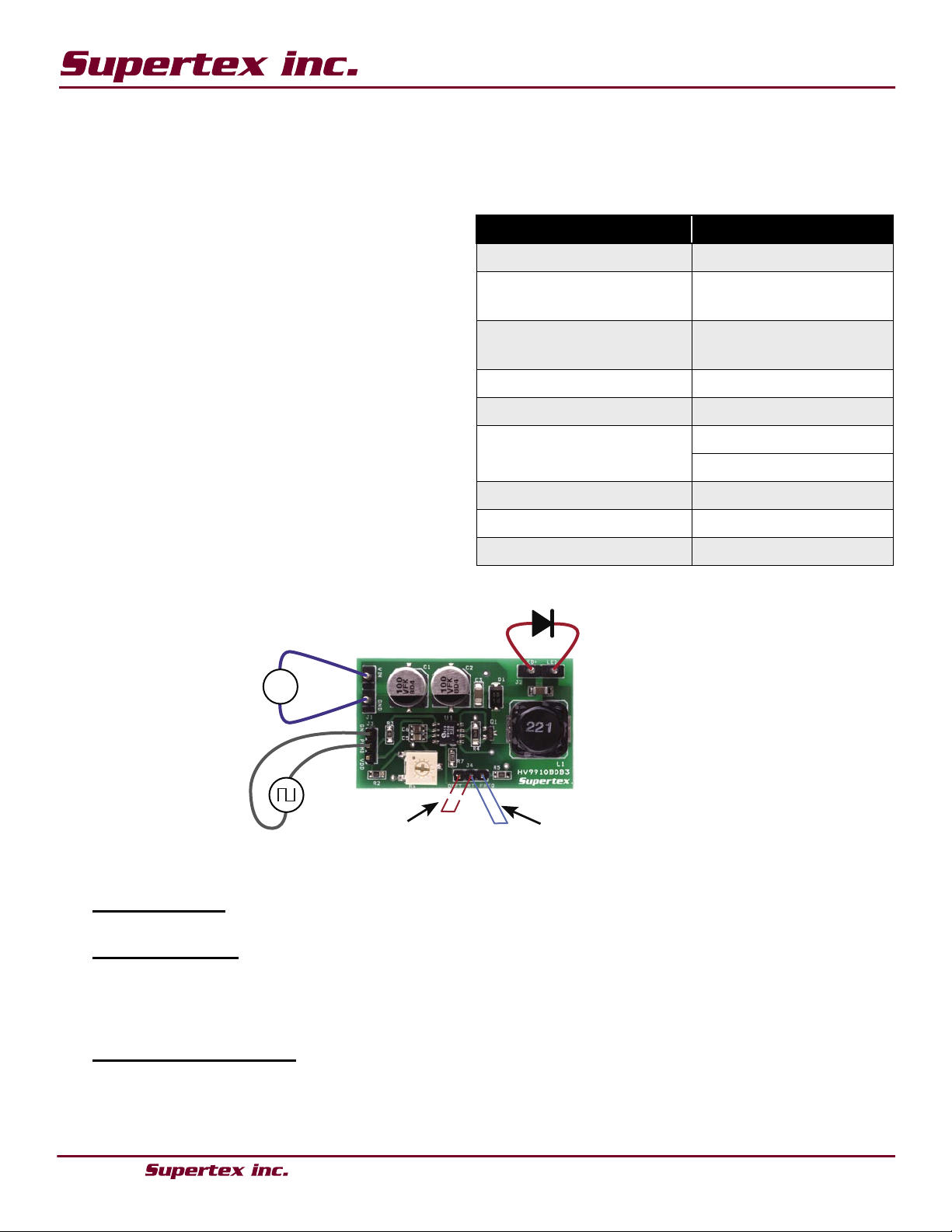
Connection Diagram
Specifications
Parameter Value
Input voltage 10 - 30VDC
Output voltage constant frequency mode
Output voltage constant off-time mode
Maximum output current 1.0A ± 10%
Output current ripple (typ) 20% (peak-peak)
86% (for one LED)
Efficiency (@ 12V input)
93% (for two LEDs)
Open LED protection yes
Output short circuit protection no
Dimensions 48.2mm X 29.0mm
2.0 - 4.5V
4.0 - 8.0V
Connections
1. Input Connection: Connect the input DC voltage between VIN and GND terminals of connector J1 as shown in the
connection diagram.
2. Output Connection: Connect the LEDs between LED+ (anode of LED string) and LED- (cathode of LED string) of
connector J2.
a. If the load is one LED, short the RT and FREQ terminals of connector J4 using a jumper.
b. If the load is two LEDs, short the RT and OFFT terminals of connector J4 using a jumper.
3. PWM Dimming Connection:
a. If no PWM dimming is required, short PWMD and VDD terminals of connector J3.
b. If PWM dimming is required, connect the TTL-compatible PWM source between PWMD and GND terminals of
connector J3. The recommended PWM dimming frequency is ≤ 1.0kHz.
1
Page 22
HV9910BDB3
● 1235 Bordeaux Drive, Sunnyvale, CA 94089 ● Tel: 408-222-8888 ● www.supertex.com
V
O,MAX
• T
OFF
L
Δl =
I
LED
= –
V
CS
R
CS
Δl
2
V
O, MAX
V
IN,MIN
1 –
Maximum Switching Frequency =
{
{
T
OFF
V
O, MAX
V
IN,MIN
1 –
{
{
L • f
S
V
O,MAX
•
I
LED
= –
V
CS
R
CS
Δl
2
Δl =
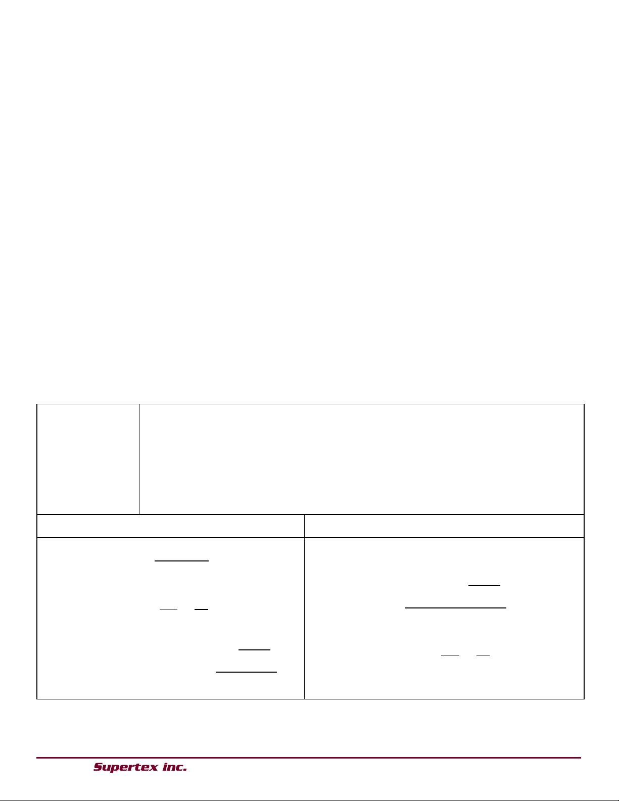
Frequently Asked Questions
1. Why does the demoboard have two operating modes?
Constant frequency mode limits the maximum output voltage to less then 50% of the minimum input voltage. So, in
this case, if we use only the constant frequency mode, the maximum output voltage will have to be less than 5V. Con
stant off-time mode removes this limitation and allows the output voltage become higher. However, in order to achieve
reasonable noise immunity and to limit the switching frequency variation over the input voltage range, it is not recommended to operate the HV9910DB3 with the output voltage exceeding 80% of the input voltage, even in the constant
off-time mode. Please refer to application note AN-H50 on the Supertex website for more details.
2. If the minimum input voltage in my application is higher (say 20V), does that mean I can drive a 9V LED string
in the constant frequency mode or an 16V LED string in the constant off-time mode using the
demoboard?
Although a larger LED string can be driven using the demoboard in these conditions, the demoboard will not be able to
drive the LED at 1A.
The HV9910B is a constant peak current controller. The average LED current is equal to the peak current set (using the
sense resistor) minus one-half of the ripple current in the inductor.
Higher output voltages lead to larger ripple current values, which will reduce the maximum LED current the board can
deliver.
-
3. How can I compute the maximum LED current the demoboard can deliver if I use a higher input voltage and a
higher LED string voltage?
Parameters Minimum input voltage
Maximum LED string voltage
Switching frequency (constant frequency mode)
Off-Time (constant off-time mode)
HV9910B CS threshold voltage
Sense Resistor
Inductor
= V
= V
= f
= T
= V
= R
= L
IN,MIN
O,MAX
S
OFF
CS
CS
(100kHz)
(5.1μs)
(0.25V)
(0.22Ω)
(220μH)
Constant Off-Time Mode Constant Frequency Mode
2
Page 23
HV9910BDB3
● 1235 Bordeaux Drive, Sunnyvale, CA 94089 ● Tel: 408-222-8888 ● www.supertex.com
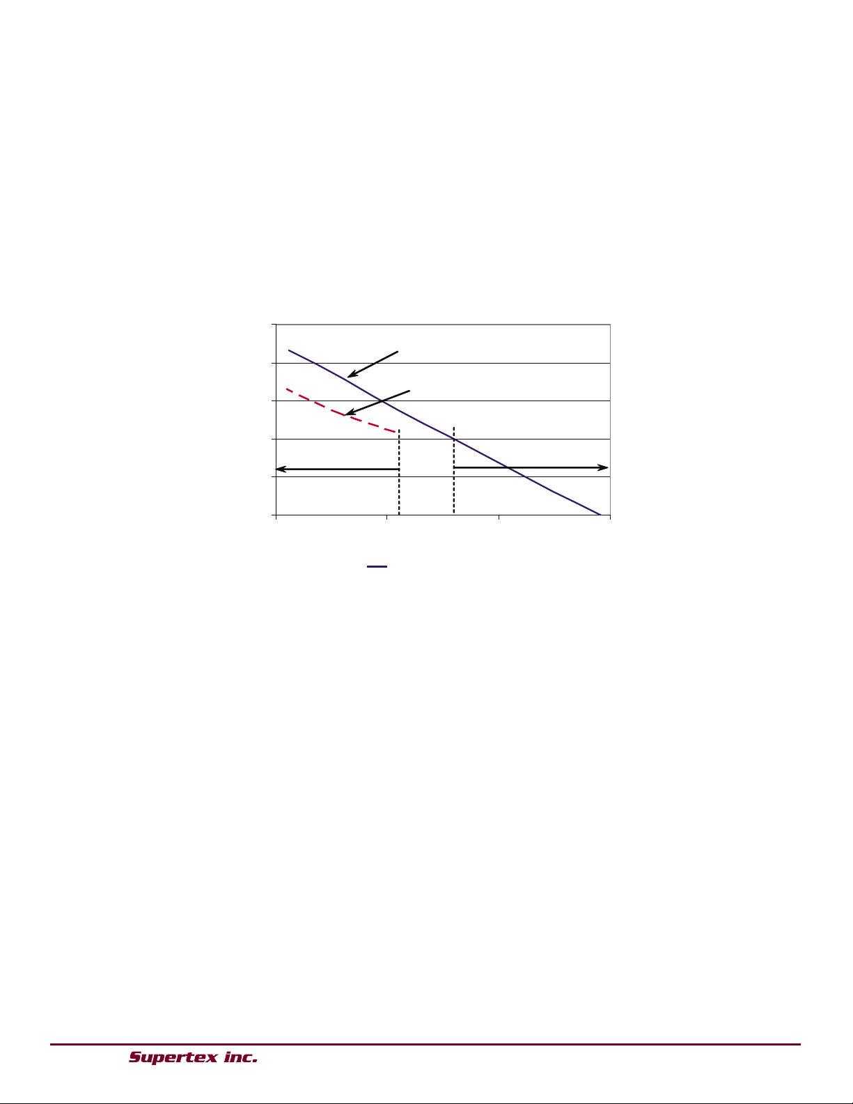
Load Regulation
(@ VIN = 12V)
0
2
4
6
8
10
2 4 6 8
Load Voltage (V)
Change in current (%)
Constant Off-Time Mode
Constant off-time mode
Constant Frequency Mode
Constant Off-time Mode
With mode chang
e
Frequently Asked Questions (cont.)
4. If the constant off-time mode allows a wider LED voltage range, why not use that mode exclusively? Why do
we need the constant frequency mode?
Although the constant off-time mode allows the demoboard to operate at a higher output voltage, the LED ripple current
is directly proportional to the output voltage in this mode. This makes it difficult to get a good load regulation of the LED
current in the constant off-time mode with a wide variation in the LED string voltage (in this case it will be a 1:4 variation).
At lower LED voltage values, the ripple will be lower and the LED current would be higher.
By switching between the two modes depending on the load, we can get a better current accuracy without having to
adjust the LD voltage or the sense resistor.
5. Why is the efficiency of the demoboard higher with a load of two LEDs compared to a single LED load?
Losses in the HV9910BDB3 occur due mainly due to two factors:
a. Conduction losses in the FET and diode
b. Switching losses in the FET
Switching losses are dependent on the switching frequency, input voltage and total parasitic capacitance at the node.
At higher switching frequencies, the switching losses are higher.
Conduction losses are dependent on the duty cycle. Since the voltage drop on the FET is smaller than the voltage drop
on the diode (the on-resistance of the FET is very small), the higher the duty cycle, the smaller is the conduction loss.
Please note that we are ignoring the losses in the inductor, which will be identical in both cases.
Also, efficiency = P
thereby the efficiency is higher.
Comparing the operation of the converter in both modes at 12V input for this particular demoboard, the following
are the differences:
input power. So, if the output power is higher, the fixed switching losses are a smaller fraction of the output power and
a. Output power is higher with 2 LEDs as the load
OUT
/ P
= P
IN
OUT
/ (P
+ losses) = 1/ (1 + losses/P
OUT
), where P
OUT
is the output power and PIN is the
OUT
b. Switching frequency in the constant off-time mode is 55kHz, whereas it is 100kHz in the constant frequency
mode
c. Duty cycle of operation is about higher in the constant off-time mode by a factor of 2 than in the constant
frequency mode
All the above factors favor the higher load voltage and thus the demoboard has a higher efficiency when the load is larger.
3
Page 24
HV9910BDB3
● 1235 Bordeaux Drive, Sunnyvale, CA 94089 ● Tel: 408-222-8888 ● www.supertex.com
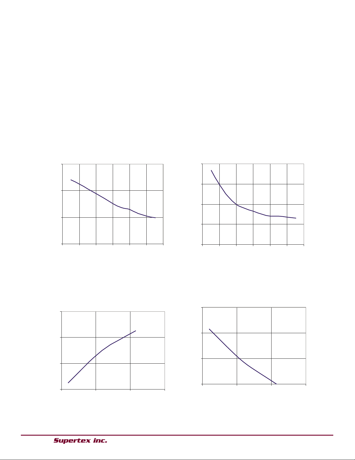
Fig. 1. Efficiency vs. Input Voltage Plot
Efficiency vs. Input Voltage (@ VO = 4V)
82
84
86
88
8 12 16 20 24 28 32
Input Voltage (V)
Efficiency (%)
Fig. 2. Line Regulation of LED Current Plot
Line Regulation (@ VO = 4V)
-2
-1
0
1
2
8 12 16 20 24 28 32
Input Voltage (V
)
Change in current (%)
Efficiency vs. Load Voltage
(@ VIN = 12V)
75
80
85
90
2 3 4 5
Load Voltage (V)
Efficiency (%)
Fig. 3. Efficiency vs. Load Voltage Plot
Load Regulation (@ VIN = 12V)
0
1
2
3
2 3 4 5
Load Voltage (V)
Change in current (%)
Fig. 4. Load Regulation of LED Current Plot
Frequently Asked Questions (cont.)
6. Why are the LED current rise and fall times during PWM dimming different when the load changes from
one LED to two LEDs?
The LED current rise time is directly proportional to V
input voltage and V
is the output voltage). Since V
OUT
- V
IN
OUT
and the fall time is proportional to V
OUT
is higher with two LEDs, the rise time will be larger and the fall
(where VIN is the
OUT
time will be smaller.
Typical Results
Constant Frequency Mode:
The HV9910BDB3 is designed to be operated in the constant frequency mode when the load is a single LED. In this
mode, the line regulation of the LED current is less than 2% and full-load efficiency greater than 80%.
4
Page 25
HV9910BDB3
● 1235 Bordeaux Drive, Sunnyvale, CA 94089 ● Tel: 408-222-8888 ● www.supertex.com
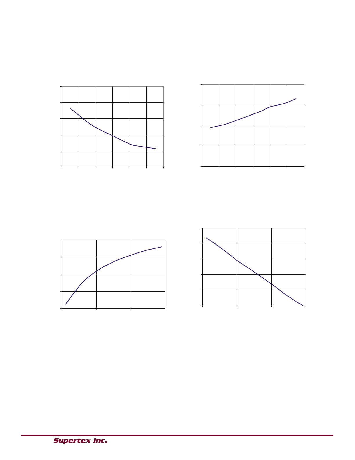
Fig. 5. Efficiency vs. Input Voltage Plot
Efficiency vs. Input Voltage
(@V
O
= 7.8V)
90
91
92
93
94
95
8 12 16 20 24 28 3
2
Input Voltage (V)
Efficiency (%)
Fig. 6. Line Regulation of LED Current Plot
Line Regulation (@ VO = 7.8V)
-2
-1
0
1
2
8 12 16 20 24 28 3
2
Input Voltage (V
)
Change in current (%)
Efficiency vs. Load Voltage
(@V
IN
= 12V)
75
80
85
90
95
2 4 6 8
Load Voltage (V)
Efficiency (%)
Fig. 7. Efficiency vs. Load Voltage Plot
Fig. 8. Load Regulation of LED Current Plot
Load Regulation (@ VIN = 12V)
0
2
4
6
8
10
2 4 6 8
Load Voltage (V)
Change in current (%)
Constant Off-Time Mode:
The HV9910BDB3 is designed to be operated in the constant off-time mode when the load is two LEDs in series. In this
mode, the line regulation of the LED current is less than 2% and the efficiency greater than 80%.
5
Page 26
HV9910BDB3
● 1235 Bordeaux Drive, Sunnyvale, CA 94089 ● Tel: 408-222-8888 ● www.supertex.com
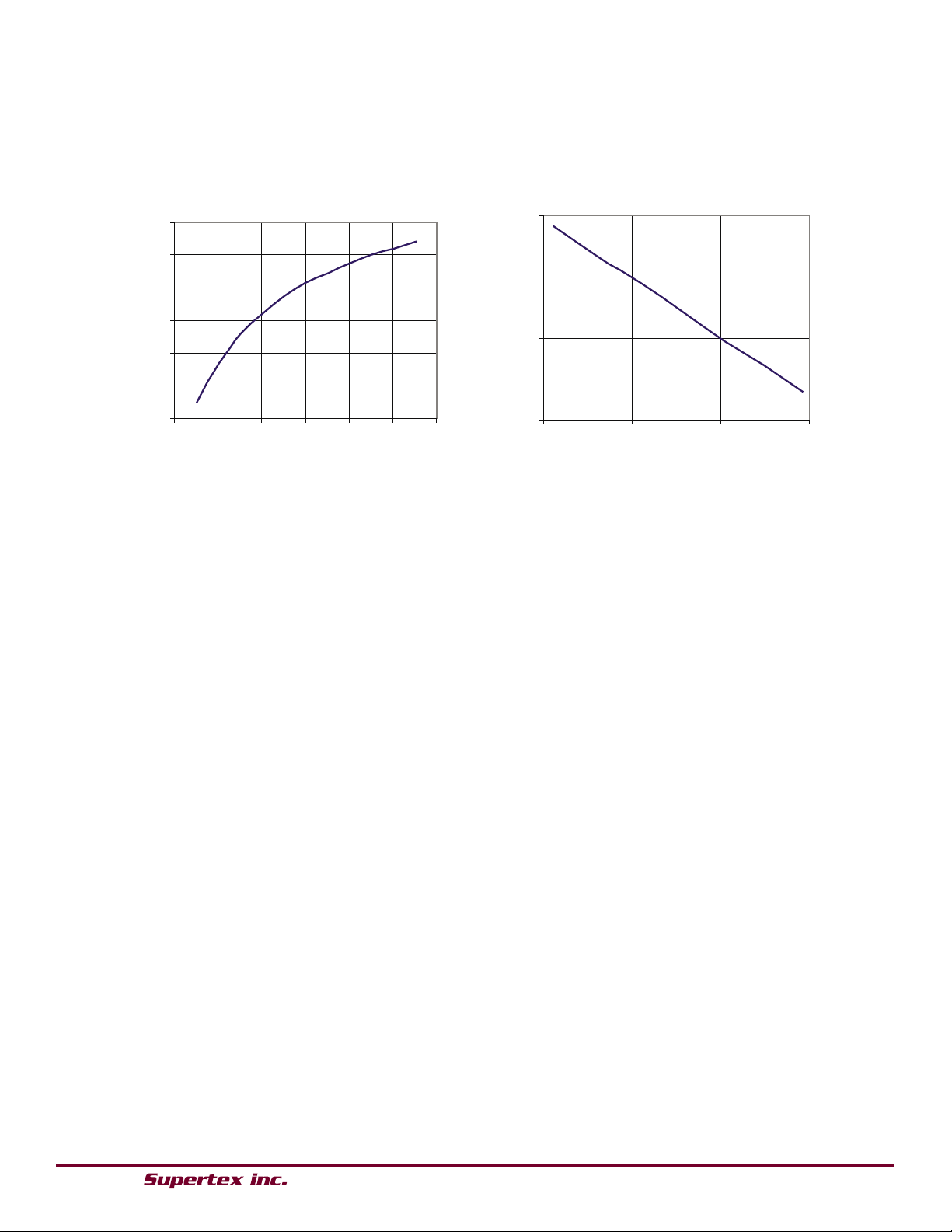
Fig. 9. Switching Frequency vs. Input Voltage Plot
Switching Frequency vs. Input Voltage
(@V
O
=7.8V)
20
40
60
80
100
120
140
8 12 16 20 24 28 3
2
Input Voltage (V)
Switching Frequency (kHz)
Fig. 10. Switching Frequency vs. Load Voltage Plot
Switching Frequency vs. Load
Vo
ltage (@VIN =12V)
40
60
80
100
120
140
2 4 6 8
Load Voltage (V
)
Switching Frequency (kHz)
The variation in the switching frequency, when the HV9910BDB3 is operated in the constant off-time mode, is shown in
Figs. 9 and 10.
6
Page 27
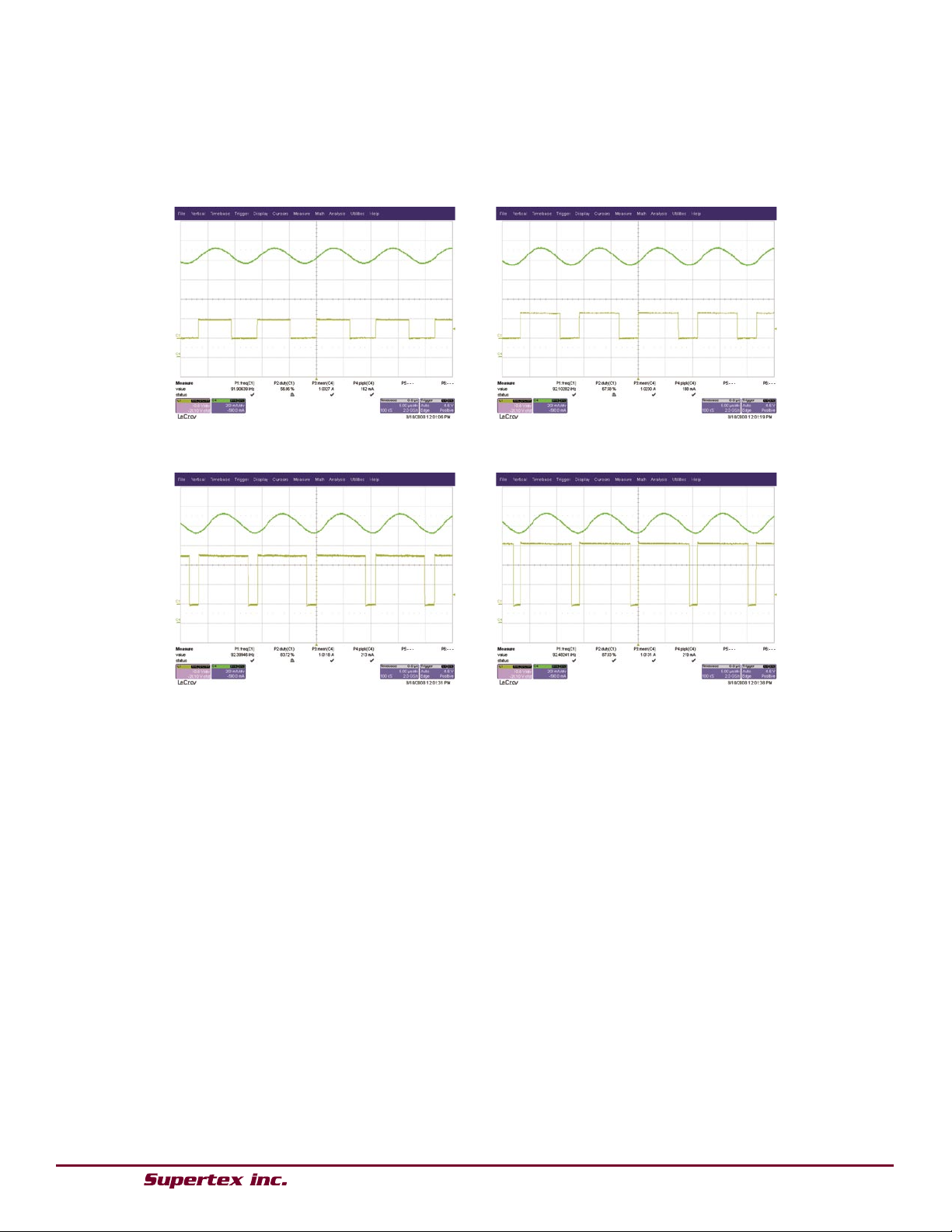
● 1235 Bordeaux Drive, Sunnyvale, CA 94089 ● Tel: 408-222-8888 ● www.supertex.com
Waveforms
(a) 10V input
Drain Voltage
LED Current
(b) 12V input
Drain Vo
ltage
LED Curren
t
(c) 24V input
Drain Voltage
LED Current
(d) 30V input
Drain Vo
ltage
LED Curren
t
Fig.11. Steady State Waveforms in Constant Frequency Mode
C1 (Yellow) : Drain Voltage (10V/div)
C4 (Green) : LED Current (200mA/div)
Ti
me Base : 5μs/div
Constant Frequency mode (LED Voltage = 3.3V):
HV9910BDB3
7
Page 28
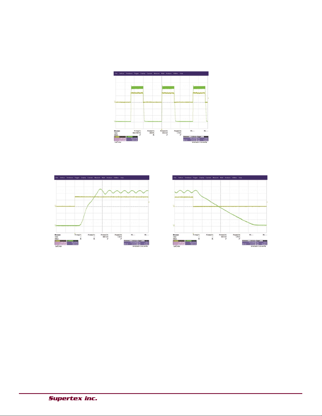
● 1235 Bordeaux Drive, Sunnyvale, CA 94089 ● Tel: 408-222-8888 ● www.supertex.com
Waveforms (cont.)
(b) PWM Dimming Fall Time
Time Scale : 10μs/di
v
PWM Dimming Input
LED Current
(a) P
WM Dimming Rise Time
Time Scale : 10μs/di
v
PWM Dimming Input
LED Current
(a) PWM Dimming Performanc
e
Time Scale
: 500μs/div
PWM
Dimming
Input
LED Current
Fig.12. PWM Dimming Performance in Constant Frequency Mode
C1 (Yellow) : PWMD Input Voltage (2V/div)
C4 (Green)
: LED Current (200mA/div)
HV9910BDB3
8
Page 29
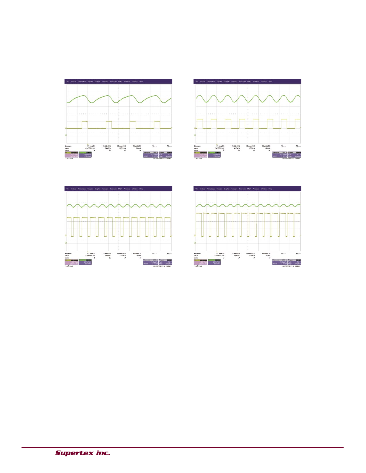
● 1235 Bordeaux Drive, Sunnyvale, CA 94089 ● Tel: 408-222-8888 ● www.supertex.com
Waveforms (cont.)
(a) 10V input
Drain Voltage
LED Current
(b) 12V input
Drain Voltage
LED Curren
t
(c) 24V input
Drain Voltage
LED Current
(d) 30V input
Drain Voltage
LED Curren
t
Fig.13. Steady State Waveforms in Constant Frequency Mode
C1 (Yellow) : Drain Voltage (10V/div
)
C4 (Green) : LED Current (200mA/div
)
Time Base : 10μs/div
Constant Off-time mode (LED Voltage = 6.4V):
HV9910BDB3
9
Page 30
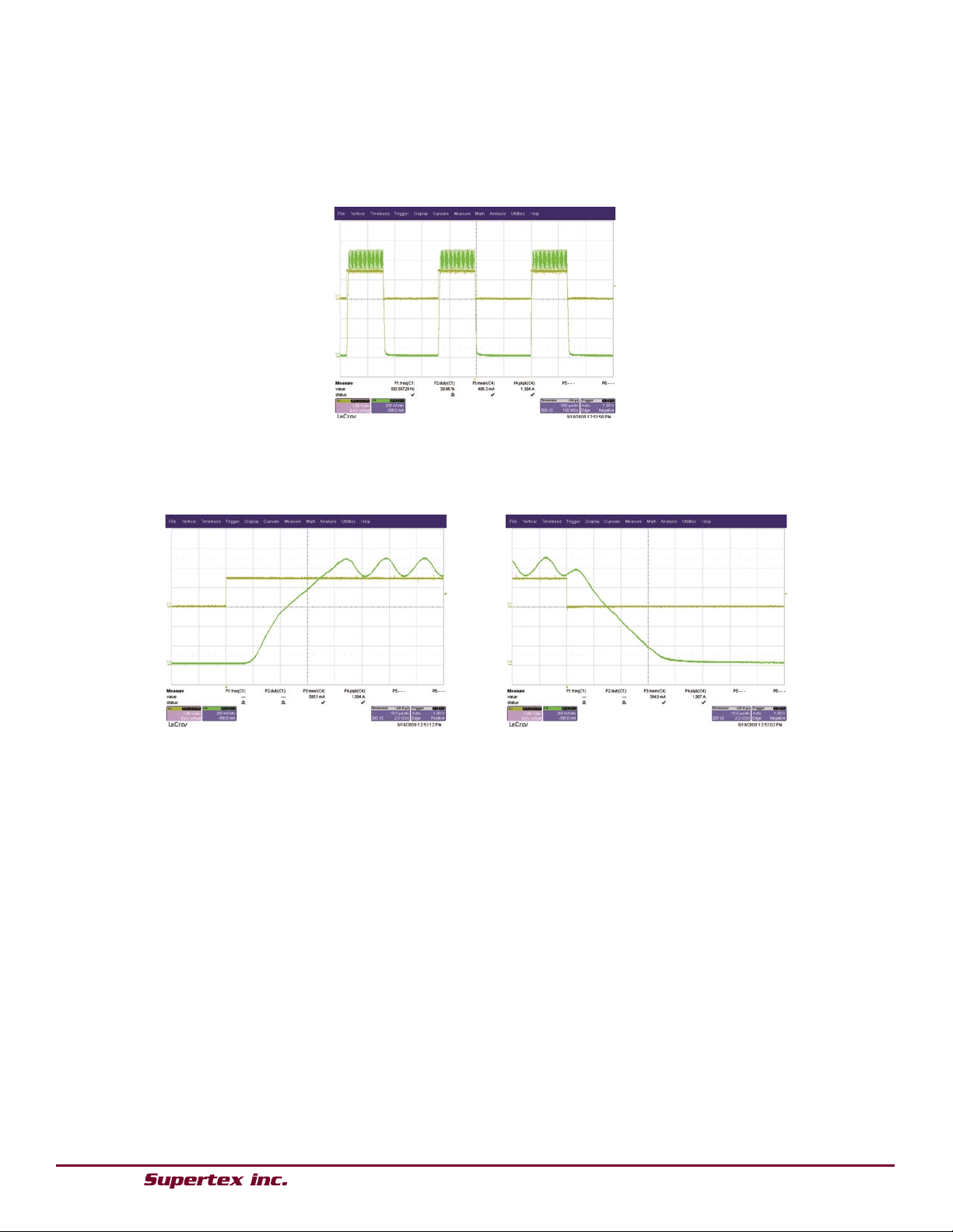
● 1235 Bordeaux Drive, Sunnyvale, CA 94089 ● Tel: 408-222-8888 ● www.supertex.com
Waveforms (cont.)
(a) PWM Dimming Fall Time
Time Scale : 10μs/di
v
PWM Dimming Input
LED Current
(b)
PWM Dimming Rise Time
Time Scale : 10μs/di
v
PWM Dimming Input
LED Current
(a) PWM Dimming Performanc
e
Time Scale : 500μs/div
PWM
Dimming
Input
LED Curren
t
Fig.14. PWM Dimming Performance in Constant Frequency Mode
C1 (Yellow) : PWMD Input Voltage (2V/div)
C4 (Green) : LED Current (200mA/div)
HV9910BDB3
10
Page 31
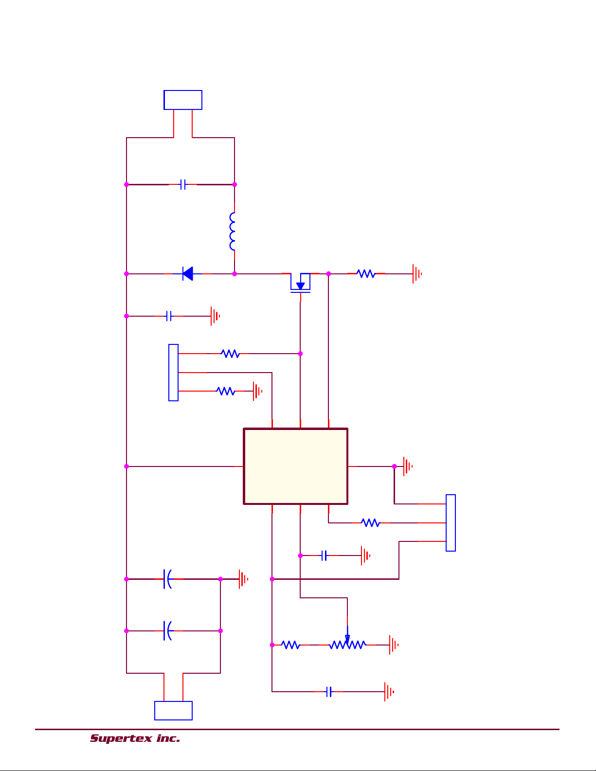
● 1235 Bordeaux Drive, Sunnyvale, CA 94089 ● Tel: 408-222-8888 ● www.supertex.com
Schematic Diagram
7
R
105k
7
R
105k
2
R
K741
2
R
K741
5
C
0.1uF, 16V
5
C
0.1uF, 16V
3
C
2.2uF, 50V
3
C
2.2uF, 50V
1
1
2
2
3
3
3J
3J
1
1
2
2
3
3
4
J
4
J
4C
2.2uF, 50V
4C
2.2uF, 50V
1
2
1J1J
3R
k
1
3R
k
1
1
7
5
3
2
4
8
6
1U
1U
1
2
2J2
J
5R
226k
5R
226k
2
C
100uF, 35V
2
C
100uF, 35V
1C
100uF, 35V
1C
100uF, 35V
1
D
3
1
-0
4
1
B
1
D
3
1
-0
4
1
B
1
2
1
L
H
u
022
1
L
H
u
022
4R
22.0
4R
22.0
6R
K5
6R
K5
1
Q
S
D
8132
i
S
1
Q
S
D
8132
i
S
6
C
2.2uF, 16V
6
C
2.2uF, 16V
VIN
LD
PWMD
GND
CS
GAT
E
ROSC
VDD
HV9910B
HV9910BDB3
11
Page 32
Supertex inc. does not recommend the use of its products in life support applications, and will not knowingly sell them for use in such applications unless it receives an
adequate “product liability indemnification insurance agreement.” Supertex inc. does not assume responsibility for use of devices described, and limits its liability to the
replacement of the devices determined defective due to workmanship. No responsibility is assumed for possible omissions and inaccuracies. Circuitry and specifications
are subject to change without notice. For the latest product specifications refer to the Supertex inc. website: http//www.supertex.com
.
©2008 All rights reserved. Unauthorized use or reproduction is prohibited .
1235 Bordeaux Drive, Sunnyvale, CA 94089
Tel: 408-222-8888
www.supertex.com
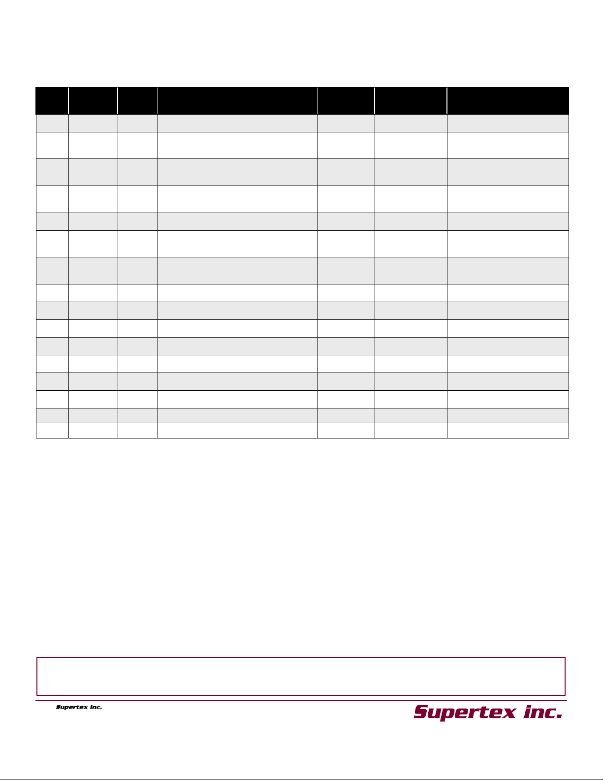
HV9910BDB3
Bill of Materials
Item
#
Quantity
Ref
Des
Description Package Manufacturer
1 2 C1,C2 100µF, 35V, electrolytic capacitor SMT Panasonic EEV-FK1V101P
2 2 C3,C4
3 1 C5
4 1 C6
2.2µF, 50V, X7R ceramic chip
capacitor
0.1µF, 16V X7R ceramic chip
capacitor
2.2µF, 16V X7R ceramic chip
capacitor
SMD1206 Murata GRM31CR71H225KA88L
SMD0805 Panasonic ECJ-2VB1C104K
SMD0805 TDK Corp C2012X7R1C225K
5 1 D1 40V, 1A schottky diode SMA Diodes Inc B140-13
6 2 J1,J2
7 2 J3,J4
2 position, 5mm pitch, vertical
header
3 position, 0.100” pitch, vertical
header
Thru-Hole
Thru-Hole Molex 22-03-2031
On Shore
Tech
8 1 L1 220uH, 1.3A rms, 2.4A sat inductor SMT Coiltronics DR127-221-R
9 1 Q1 40V, 45mΩ, 10nC N-channel FET SOT-23 Vishay Si2318DS
10 1 R2 147KΩ, 1/8W, 1% chip resistor SMD0805 - -
Manufacturer’s Part
Number
EDSTL130/02
11 1 R3 1kΩ, 1/8W, 1% chip resistor SMD0805 - -
12 1 R4 0.22Ω, 1/4W, 1% chip resistor SMD1206 - -
13 1 R5 226kΩ, 1/8W, 1% chip resistor SMD0805 - -
14 1 R6 5KΩ top adjust trimpot SMT Bourns Inc 3361P-1-502G
15 1 R7 105kΩ, 1/8W, 1% chip resistor SMD0805 - -
16 1 U1 Universal LED Driver SO-8 Supertex HV9910BLG-G
082608
12
Page 33
● 1235 Bordeaux Drive, Sunnyvale, CA 94089 ● Tel: 408-222-8888 ● www.supertex.com
HV9910B PFC 40W
LED Driver Demoboard
HV9910BDB7
General Description
The Supertex HV9910BDB7 demonstrates the use of an
HV9910B control IC in an off-line, High Brightness LED driver
application. The board incorporates power factor correction
(PFC) and satisfies the limits for harmonic currents according
to the EN61000-3-2 Class C standard having total harmonic
distortion (THD) less than 20%. The board features a low
component count and long life operation due to the absence
of electrolytic capacitors. The board is designed to supply a
string of LEDs with a current of 350mA and a voltage in the 65
to 105V range from a 220/230VAC line.
The conversion stage draws line current throughout the AC
line cycle, partly using a charge pumping and partly using a
boost conversion technique to charge the bulk energy storage
capacitors. The LED current is provided with a continuous
mode buck stage giving a DC current with about 30% peak-topeak ripple. A patent for this conversion technique is pending.
Please inquire with the Supertex applications department for
design guidance, should change of input line voltage, output
voltage, or output current be desired.
An effort was made to satisfy the requirements of CISPR
15 (EN55015), limits and methods of measurement of radio
disturbance characteristics of electrical lighting and similar
equipment.
Specifications
Parameter Value
Input voltage 190~265VAC, 50Hz
Power factor 0.95
Total harmonic distortion
EMI limits CISPR 15
Output voltage 65~105V
Output current 350mA±10%
Output power 40W
Efficiency
Load regulation <3%
AC Line regulation <1.5%
Output ripple <30% peak-peak
Life time Non-Electrolytic
Output short circuit
protection
Output open circuit
protection
Dimensions
EN 61000-3-2 Class C
3.0” x 2.3” x 1.1”
(76mm x 58mm x 28mm)
<20%;
90%
No
Yes
The connection diagram details the hookup of the board to
the AC line. Note that the load is
and that measurements to the board require measurement
techniques in common use with non-isolated off-line power
supplies (isolation transformers, differential probes, etc).
NOT galvanically isolated,
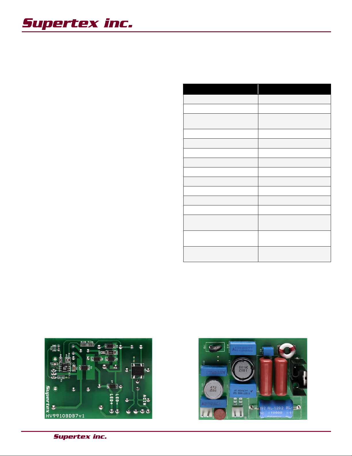
Board Layout
Top View
Actual Size: 3.0” x 2.3” x 1.1”
Bottom View
Page 34
● 1235 Bordeaux Drive, Sunnyvale, CA 94089 ● Tel: 408-222-8888 ● www.supertex.com
190 … 265V
RMS
BR1
DF04S
1
6
2
L2
560μ
H
M1
SPP04N50C3
L1
10mH
D1
STTH1R06
A
NE
G
PO
S
R20
2.2k
Ω
C2
0
100pF
C8
10μ
F
D9
S1
J
L3
4.7m
H
C11
100nF
AC
AC
F1
1A
F
3 4
1
2
J1
HDR
C10
220nF
C1
2.2μ
F
4
8
7 5 3
CT1
1:
1
C3
10n
F
D3
STTH1L06
A
D2
STTH1L06
A
J2
HDR
IC1
HV9910BNG-G
1 2
43
CL
CL-140
C7
100pF
105VDC
350mADC
D4
STTH1L06
A
C2
2.2μ
F
C5
470n
F
R6
620mΩ
R1
6
620mΩ
R4
1.0kΩ
R1
464kΩ
R12A
499k
Ω
R12B
499k
Ω
R11A
10kΩ
C1
2
100nF
VIN
GATE
CS
VDD
ROSC
LD
PW
M
GN
D
HV9910B
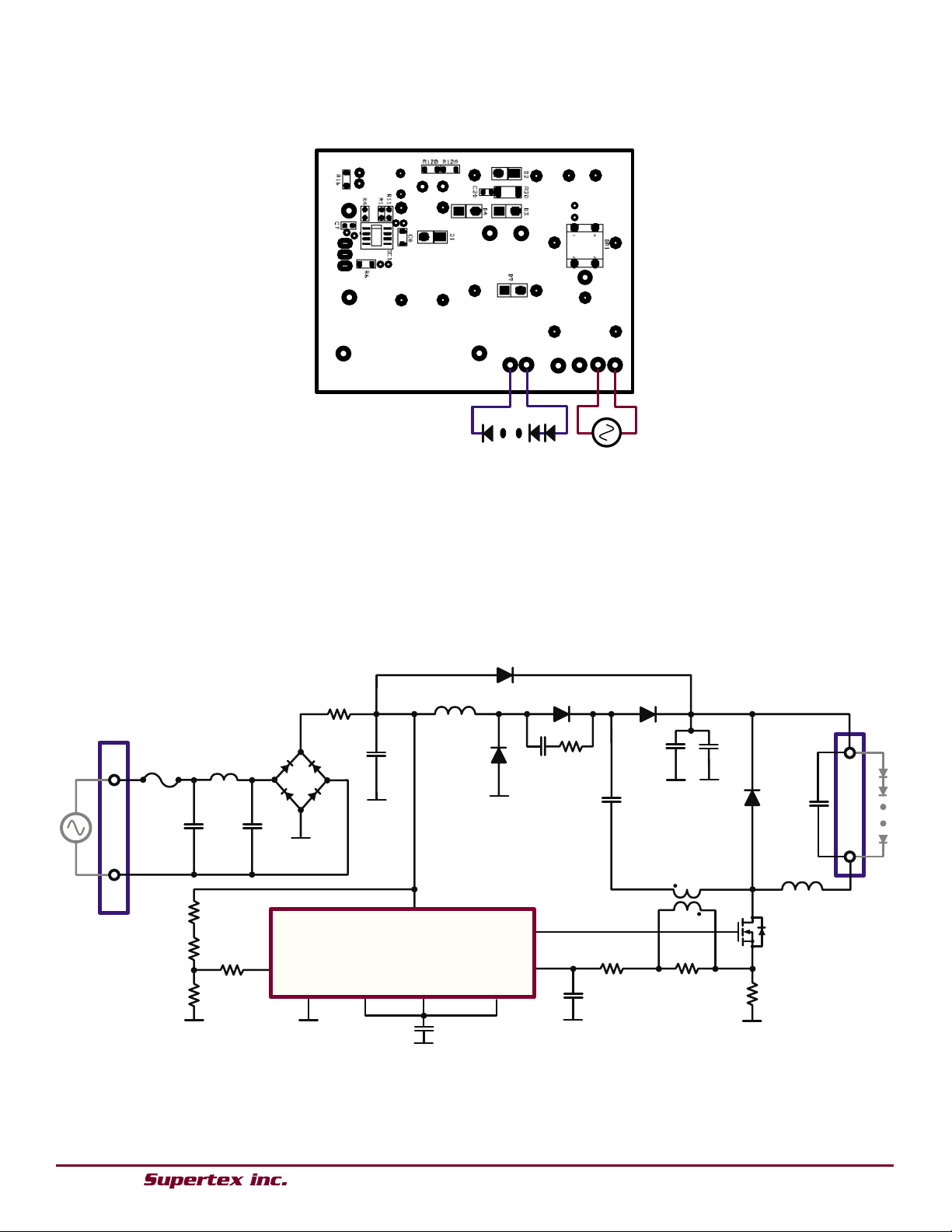
Connection Diagram
220VAC
105VDC
350mADC
HV9910BDB7
Connections
Input Voltage - Connect the AC line input voltage to AC
VIN as shown.
Schematic Diagram
LED String - Connect the LED strings between LED+ and
LED- as shown (anode of the string to LED+ and cathode
to LED-).
2
Page 35
HV9910BDB7
● 1235 Bordeaux Drive, Sunnyvale, CA 94089 ● Tel: 408-222-8888 ● www.supertex.com
I
LED
Load Regulation (VIN = 230VAC)
0.348
0.35
0.35
2
0.354
0.35
6
0.35
8
0.36
0.36
2
0.36
4
0.36
6
104.3 84.
4 67.5
V
O
I
LED
I
LED
Line Regulation (VO = 105V)
0.349
0.35
0.351
0.352
0.353
0.354
0.355
0.356
0.357
0.358
190 210 230 250 270
V
AC
I
LED
Harmonic Distortion (VO = 105V, I
LED
= 350mA)
0
5
10
15
20
25
30
35
40
190 210 230 250 27
0
V
AC
THD,%
Power Factor (VO = 105V, I
LED
= 350mA)
0.87
0.88
0.89
0.
9
0.91
0.92
0.93
0.94
0.95
0.96
190 210 230 250 270
V
AC
PF
Efficiency (V
LED
= 105V, I
LED
= 350mA)
0.885
0.89
0.89
5
0.
9
0.90
5
0.91
190 210 230 250 27
0
V
AC
EFF
Efficiency (V
IN
= 230VAC, I
LED
= 350mA)
0.85
0.86
0.87
0.88
0.89
0.
9
0.91
104.3 84.4 67.
5
V
O
EFF
Typical Characteristics
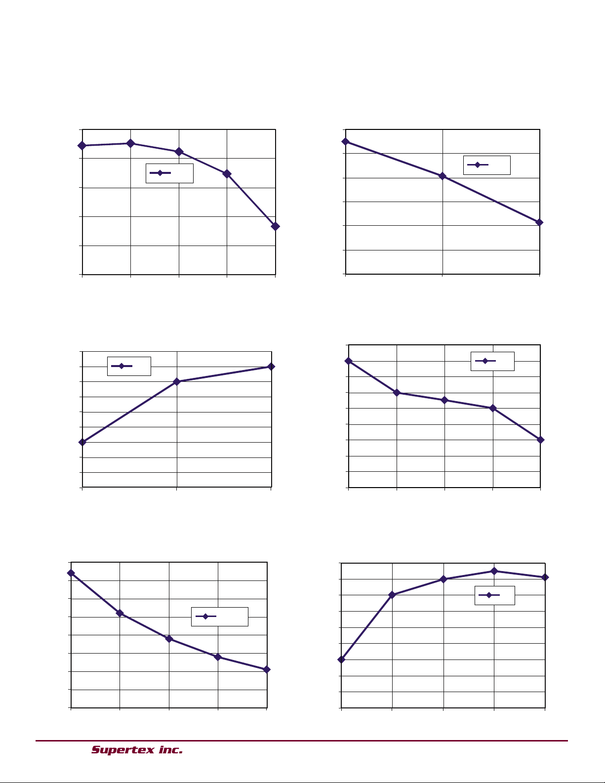
Figure 1. Efficiency at full load. Figure 2. Efficiency at nominal AC line voltage.
Figure 3. Load regulation. Figure 4. AC line regulation.
Figure 5. Harmonic Distortion vs. AC Line Voltage.
Figure 6. Power Factor vs. AC Line Voltage.
3
Page 36
● 1235 Bordeaux Drive, Sunnyvale, CA 94089 ● Tel: 408-222-8888 ● www.supertex.com
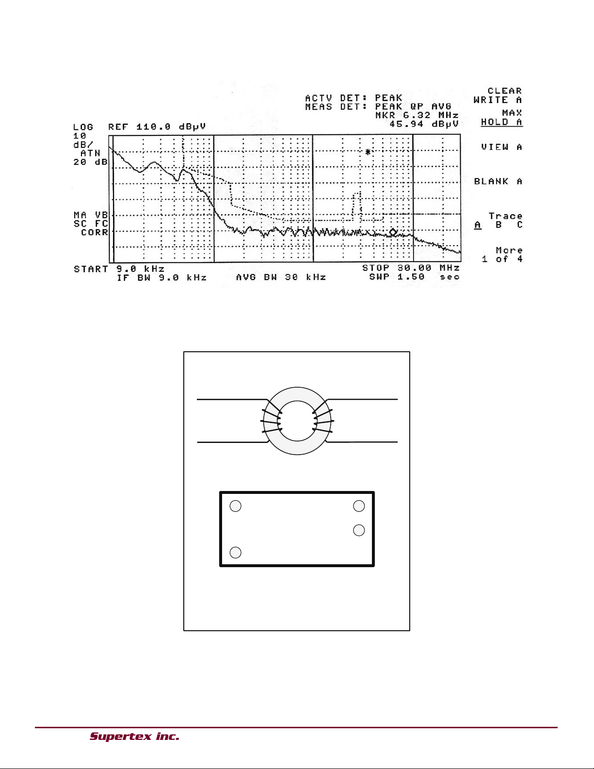
Figure 7. EMI Characterization - Conducted Emissions vs CISPR 15 Limits.
1
2
4
3
1
2
4
3
TOP VIEW
Vertical Toroid Mount
Mfr: Lodestone Pacific
PN: VTM455-4 CT1
4T : 4T
AWG2
4
Mfr: Ferroxcube
PN: TN/10/6/
4
HV9910BDB7
Figure 8. CT1 Construction Diagram.
4
Page 37

Supertex inc. does not recommend the use of its products in life support applications, and will not knowingly sell them for use in such applications unless it receives
an adequate “product liability indemnification insurance agreement.”
Supertex inc. does not assume responsibility for use of devices described, and limits its liability
to the replacement of the devices determined defective due to workmanship. No responsibility is assumed for possible omissions and inaccuracies. Circuitry an
d
specifications are subject to change without notice. For the latest product specifications refer to the
Supertex inc. (website: http//www.supertex.com)
©2009 Supertex inc. All rights reserved. Unauthorized use or reproduction is prohibited.
Supertex inc.
1235 Bordeaux Drive, Sunnyvale, CA 94089
Tel: 408-222-8888
www.supertex.com
HV9910BDB7
Bill of Materials
Qty Ref Des Description Manufacturer Part Number
1 BR1 Rect Bridge, DFS, 400V, 1.5A Fairchild Semi DF04S
2 C1, C2 Cap, MZPEF, 450VDC, 10%, 2.2UF Panasonic ECG ECQ-E2W225KH
1 C3 Cap, MZPEF, 630VDC, 5%, 10NF EPCOS Inc B32529C8103J
1 C5 Cap, MZPEF, 400V, 10%, .47UF EPCOS Inc B32522C6474K
1 C7 Cap, CER, NP0, 50V, 10%, 0805, 100PF Kemet C0805C101K5GACTU
1 C8 Cap, CER, X7R, 10V, 10%, 1206, 10UF Murata GRM31CR71A106KA01L
1 C20 Cap, CER, NP0, 1000V, 5%, 0805, 100PF Vishay/Vitramon VJ0805A101JXGAT5Z
1 C10 Cap, MKP, 220NF, 305VAC, X2, 125C, 20% EPCOS Inc B32922T2224M
2 C11, C12 Cap, MKP, 100NF, 305VAC, X2, 125C, 20% EPCOS Inc B32922A2104M
1 CL1 Inrush current limiter, 50/0.89Ω, 1.1A GE Sensing CL-140
1
1 Toroidal core mount, 0.455Dia, 4PIN Lodestone Pacific VTM455-4T
CT1
Core, toroidal, TN10/6/4-3E25 Yageo / Ferroxcube TN10/6/4-3E25
AR Magnet wire, MW28C, SPN AWG24 MWS Wire Industries SPN AWG24
1 D1 Diode, ultrafast, 600V, 1A, SMA STMicroelectronics STTH1R06A
3 D2, D3, D4 Diode fast, 600V, 1A ,SMA STMicroelectronics STTH1L06A
1 D9 Rectifier, GPP, 600V, 1A, SMA Diodes Inc S1J-13-F
1 F1 Fuse fast, 1.00A, IEC, Short, TR5 Wickmann USA 37011000410
1 HS1 Heatsink, TO-220, Ver MNT W/Tab, H75 21K Aavid Thermalloy 574502B03700G
1 IC1 IC, LED Driver, 8-Lead SOIC Supertex HV9910BLG-G
2 J1, J2 Header, 2POS, .156, VERT TIN Molex 26-48-1021
1 L1 Choke AXL,14mm, 10mH, 10%, 350mA Renco RL-1292-10000
1 L2 Choke SH RAD,16mm, 10%, 560µH, 1.1A Sumida RCR1616NP-561K
1 L3 Choke SH RAD,13mm, 15%, 4.7mH, 370mA Sumida RCP1317NP-472L
1 M1 MOSFET, N-CH, 560V, 4.5A, TO-220AB Infineon Technologies SPP04N50C3
1 R1 Resistor 1/8W, 1%, 0805, 464KΩ Panasonic ECG ERJ-6ENF4643V
1 R4 Resistor 1/8W, 1%, 0805, 1.00KΩ Panasonic ECG ERJ-6ENF1001V
1 R11 Resistor 1/8W, 1%, 0805, 10.0KΩ Panasonic ECG ERJ-6ENF1002V
2 R12A, R12B Resistor 1/4W, 1%, 1206, 499KΩ Panasonic ECG ERJ-8ENF4993V
1 R20 Resistor 1/2W, 5%, 2010, 2.2KΩ Panasonic ECG ERJ-12ZYJ222U
2 R6, R16 Resistor 1/2W, 1%, 1206, .62Ω Susumu Co Ltd RL1632R-R620-F
010510
5
Page 38
Supertex inc.
Buck-based LED Drivers
Using the HV9910B
AN-H48
Application Note
Fundamental Buck Converter topology is an excellent
choice for LED drivers in off-line (as well as low-voltage)
applications as it can produce a constant LED current at
very high efciencies and low cost. A peak-current-controlled
buck converter can give reasonable LED current variation
over a wide range of input and LED voltages and needs
little effort in feedback control design. Coupled with the fact
that these converters can be easily designed to operate at
above 90% efciency, the buck-based driver becomes an
unbeatable solution to drive High Brightness LEDs.
The Supertex HV9910B provides a low-cost, low component
count solution to implement the continuous mode buck
converter. HV9910B has two current sense threshold voltages
– an internally set 250mV and an external voltage at the
LD pin. The actual threshold voltage will be the lower of the
internal 250mV and the voltage at the LD pin. The low sense
voltage allows the use of low current sense resistor values.
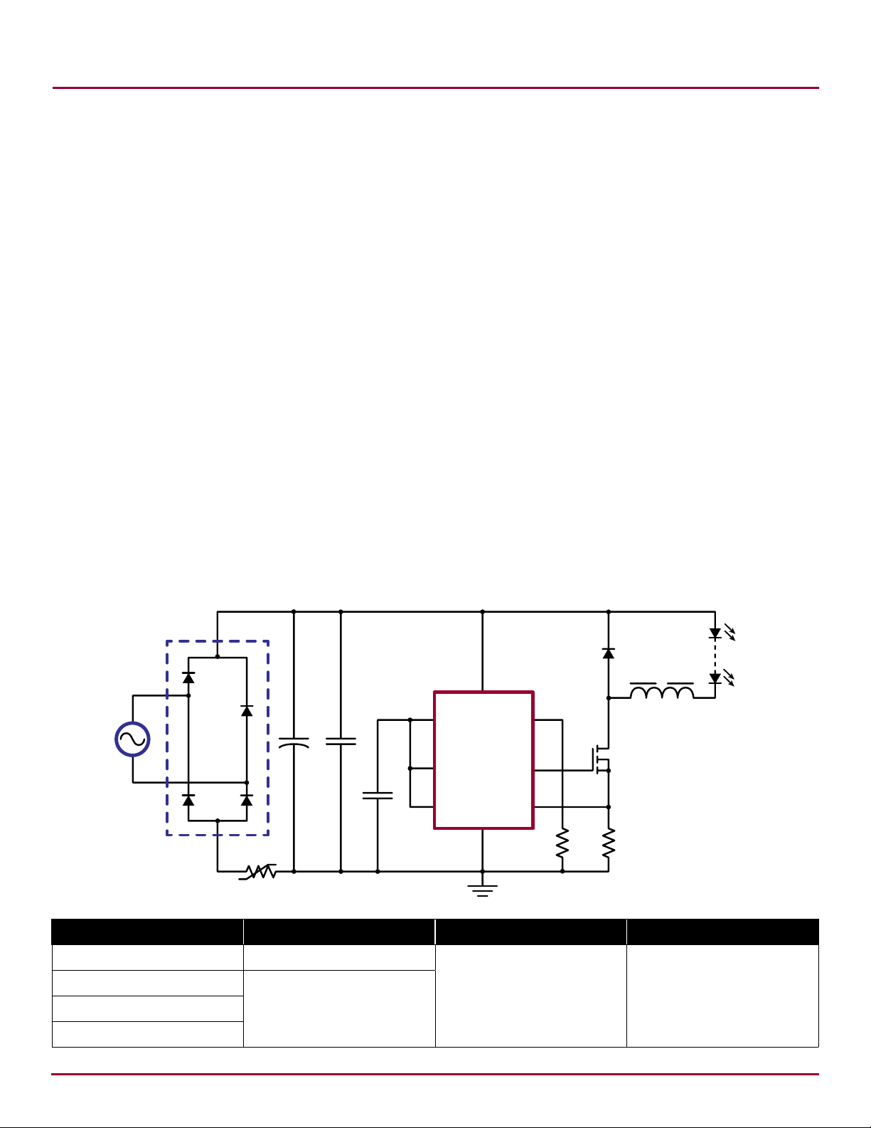
Circuit Diagram
D1
HV9910B operates down to 8V input, which is required for
automobile applications, and can take a maximum of 450V
input, which makes it ideal for off-line applications. It also
has an internal regulator that supplies power to the IC from
the input voltage, eliminating the need for an external low
voltage power supply. It is capable of driving the external
FET directly, without the need for additional driver circuitry.
Linear or PWM dimming can also be easily implemented
using the HV9910B.
This Application Note discusses the design of a buck-based
LED driver using the HV9910B with the help of an off-line
application example. The same procedure can be used to
design LED drivers with any other lower voltage AC or DC
input; 12V for example.
The information in this Application Note also applies to the
Supertex HV9910.
D2
L1
VIN
C
C
1
2
VDD
RT
LED(s)
HV9910B
Q1
R
R
1
2
NTC1
LD
C
3
PWMD
GND
GATE
CS
AC Input Voltage Range Expected LED string voltage Stabilized LED current Expected Efciency
V
= 120V rms V
NOM,AC
V
= 90V rms
MIN,AC
= 135V rms
MAX,AC
V
O,MIN
O,MAX
= 20V
= 40VV
I
350mA η = 0.9
O,MAX
freq = 60Hz
Supertex inc. ● 1235 Bordeaux Drive, Sunnyvale, CA 94089 ● Tel: 408-222-8888 ● www.supertex.com
Page 39

AN-H48
V
x I
Step 1: Switching Frequency and resistor (R1)
The switching frequency determines the size of the inductor L1 and size or type of input lter capacitor C1. A larger
switching frequency will result in a smaller inductor, but will
The hold-up and input lter capacitor required at the the diode bridge output have to be calculated at the minimum AC
input voltage. The minimum capacitor value can be calculated as:
increase the switching losses in the circuit. For off-Line applications, typical switching frequencies should be in range
(5)
20KHz-150KHz. The higher the input voltage range (for example in Europe 230VAC), the lower the frequency should
be to avoid extensive capacitive losses in the converter. For
In this example, C
North America AC line a frequency of fS = 100kHz is a good
compromise. From the datasheet, the oscillator resistor
needed to achieve this is 228kΩ.
Step 2: Choose the Input Diode Bridge (D1)
and the thermistor (NTC1)
The voltage rating of the diode bridge will depend on the
maximum value of the input voltage. The current rating will
depend on the maximum average current drawn by the con-
verter.
V
I
The 1.5 factor in equation (1) a 50% safety margin is more
than enough. For this design, choose a 400V, 1.0A diode
bridge.
Placing a thermistor (or resistor) in series with input bridge
rectier will effectively limit the inrush charging current to input bulk capacitor C1 during the initial start-up of the convert-
er. Except this useful action during very short time interval,
such a series element creates a unnecessary power loss
dissipation during normal operation of the converter, and
must be minimized. A good rule of thumb is that the thermistor should limit the inrush current to not more than ve times
the steady state current as given by equation (2), assuming
maximum voltage is applied. The required cold resistance is:
R
= 1.5 • (√2 • V
BRIDGE
=
BRIDGE
=
COLD
V
O,MAX
V
V
5 • I
) (1)
MAX,AC
• I
O,MAX
(2)
• η
MIN, DC
BRIDGE
(3)
BRIDGE
Note: Equation (5) yields a conservative estimate to
for the least amount of capacitance required. It means
that the capacitor lter will normally care large ripple
content. Some electrolytic capacitors may not be able
to withstand such ripple current and minimum value of
C1 capacitor may not be met, forcing the design to use
larger value capacitor. In the case where the allowable
ripple at the input of the buck converter is large, the
capacitor C1 can be reduced signicantly. See the Appendix for a more accurate calculation of the required
capacitor value.
The voltage rating of the capacitor should be more than the
peak input voltage with 10-12% safety margin.
V
Choose a 250V, 33µF electrolytic capacitor.
Such electrolytic capacitors have a sizable ESR component.
The large ESR of these capacitors makes it inappropriate
to absorb the high frequency ripple current generated by
the buck converter. Thus, adding a small MLCC capacitor
in parallel with the electrolytic capacitor is a good option to
absorb the high frequency ripple current. The required high
frequency capacitance can be computed as:
C2 =
In this design example, the high frequency capacitance required is about 250V, 22µF.
Step 4: Choose the Inductor (L1)
This gives us a 200Ω resistance at 25°C. Choose a thermistor with a resistance around 200Ω and rms current greater
than 0.2A for that application.
Step 3: Choose the Input Capacitors (C1/C2)
The rst design criterion to meet is that the maximum LED
string voltage is should be less than half the minimum input
voltage to avoid having to implement a special loop compen-
sation technique. For this example, the minimum rectied
voltage should be:
V
MIN,DC
= 2 • V
= 80V (4)
O,MAX
The inductor value depends on the ripple current in the
LEDs. Assume a +/- 15% ripple (a total of 30%) in the LED
current, an aggressive assumption would go up to +/-30% to
reduce the size of the inductor more than twice at the price
of reduced efciency and, possibly, reduced LED lifetime.
Then, the inductor L1 can be computed at the rectied value
of the nominal input voltage as:
(8)
C1 ≥
MAX,CAP
(fS • 0.05 • V
L1 =
2
2 x V
≥ 26.45µF.
1
≥ √2 • V
I
O,MAX
V
x 1-
O,MAX
O,MAX
MIN,AC
MAX,AC
- V
O,MAX
2
MIN,DC
→ V
x η x freq
≥ 191V (6)
MAX,CAP
• 25
(7)
)
MIN,DC
]
0.3 x I
V
√2 x V
x fS
O,MAX
O,MAX
AC,NOM
]
Supertex inc. ● 1235 Bordeaux Drive, Sunnyvale, CA 94089 ● Tel: 408-222-8888 ● www.supertex.com
2
Page 40

Supertex inc.
94089
.supertex.com
AN-H48
]
]
In this example, L1 = 2.9mH.
The peak current rating of the inductor will be:
IP = 0.35 • 1.15 = 0.4A (9)
The rms current through the inductor will be the same as
the average current for the chosen 30% ripple.Right inductor
for this application is an off-the-shelf 2.7mH, 0.54A (peak),
0.33A (rms) inductor.
Step 5: Choose the FET (Q1) and Diode (D2)
The peak voltage seen by the FET is equal to the maximum
input voltage. Using a 50% safety rating,
V
The maximum rms current through the FET depends on the
maximum duty cycle, which is 50% by design. Hence, the
current rating of the FET is:
I
Typically a FET with about 3 times the current is chosen to
minimize the resistive losses in the switch.
For this application chose a 300V, <1A MOSFET, such as a
BSP130 from Phillips. Actual MOSFET type should be de-
termined by the transistor permitted power dissipation on
printed board. For example, a BSP130 SOT-223 package
limits the dissipation to less than a Watt at 50+ Celsius, even
if the MOSFET peak current capability is 1.5A. A good rule
of thumb is to limit overall MOSFET power dissipation to
not more than 3-5% of total output power, by making a right
transistor choice. In choosing MOSFET transistors for such
LED drivers, going bigger does not mean getting better, just
the opposite. Using TO-220 transistor 500/4A/2W instead
of SOT-223 transistor 300V/0.5A/6W does more harm than
good, reducing overall efciency by several percent.
The peak voltage rating of the diode is the same as the FET.
Hence,
V
The average current through the diode is:
I
= 1.5 • (√2 • 135) = 286V (10)
FET
FET
DIODE
DIODE
≈ I
• √0.5 = 0.247A (11)
O,MAX
= V
= 286V (12)
FET
= 0.5 • I
= 0.175A (13)
O,MAX
Step 6: Choose the Sense Resistor (R2)
The sense resistor value is given by:
R2 =
if the internal voltage threshold is being used. Otherwise,
substitute the voltage at the LD pin instead of the 0.25V in
equation (14).
For this design, R2 = 0.55Ω. Also calculate the resistor power
dissipation:
PR2 = (I
A 0.1W resistor is good for this application.
Note:
Capacitor C3 is a bypass capacitor. A typical value of 1.0 to
2.2µF, 16V is recommended.
0.25
1.15 • I
O,MAX
)2 • R2 = 0.067W (15)
O,MAX
(14)
Design for DC/DC Applications
The same procedure can be used for DC/DC applications
(like the HV9910DB3). The only modications are that the
input diode bridge and input hold-up capacitor are not re-
quired. A small input capacitance to absorb high frequency
ripple current is all that is required. This capacitance can be
computed using equation (7).
Appendix
The more accurate equations for computing the required capacitance values are:
]
(16)
For the example in this application note, the actual minimum
capacitance required from the above equations is 19µF (as
compared to 26µF from equation (5)).
=
t
1
C1 ≥
1
2 x π x freq
2 x V
O,MAX
2 x V
x I
2
-1
sin
O,MAX
MIN,AC
V
√2 x V
]
x t1 +
2
- V
MIN,DC
MIN,DC
MIN,AC
4 x freq
]
1
]
(17)
x η
Choose a 300V, 1A ultra-fast diode.
Supertex inc. does not recommend the use of its products in life support applications, and will not knowingly sell them for use in such applications unless it receives
an adequate “product liability indemnification insurance agreement.” Supertex inc. does not assume responsibility for use of devices described, and limits its liability
to the replacement of the devices determined defective due to workmanship. No responsibility is assumed for possible omissions and inaccuracies. Circuitry and
specifications are subject to change without notice. For the latest product specifications refer to the Supertex inc. (website: http//www.supertex.com)
©2011 Supertex inc. All rights reserved. Unauthorized use or reproduction is prohibited.
022509
1235 Bordeaux Drive, Sunnyvale, CA
3
Tel: 408-222-8888
www
Page 41
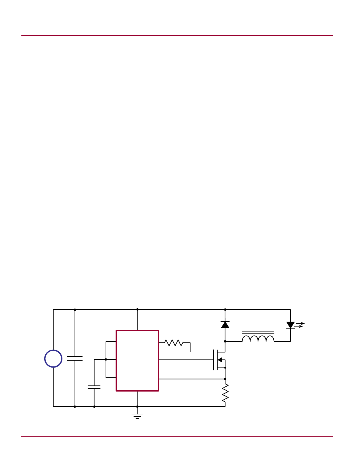
Supertex inc.
Constant, Off-time, Buck-based, LED Drivers
Using the HV9910B
AN-H50
Application Note
Constant frequency, peak current controlled buck converters
(Fig. 1) are an excellent choice for driving LEDs for a number
of reasons:
► Reasonable regulation of LED current over wide
variations in input and output voltages.
► Simple to design as no feedback compensation
is required.
► PWM dimming response of the converters is
almost instantaneous.
However, peak current controlled buck converters go into
sub-harmonic oscillations at duty cycles over 50%. These
oscillations cause the average output current to drop, while
the output ripple current increases. The only way to avoid
these problems is by adding slope compensation circuitry
externally. The slope compensation adds an upward slope
on to the current sense signal and the converter can be
stabilized by varying the slope of the added ramp (Fig.
2). This added ramp causes an error between the sensed
current (as seen at the CS pin of the HV9910B) and the
actual LED current.
Although this error can be compensated for by changing the
sensed resistor appropriately, the converter’s rejection of
the input and output voltage variations will be signicantly
degraded. Thus, changing the input or output voltage will
signicantly change the LED current, without additional
feedback circuitry for regulating the LED current. This
makes the peak current controlled buck converter practically
useless for cases where the input voltage is less than twice
the output voltage.
This problem can be overcome by changing the control
method to a constant off-time operation. In this case, the off-
time is xed by design, the on-time is based on the current
sense signal and the switching time-period adjusts to be
equal to the on-time plus the off-time. This change will allow
the converter to work with greater than 50% duty cycles and
still have the advantages of the peak current controlled buck
converter given above.
The information in this Application Note also applies to the
Supertex HV9910.
Fig. 1. Constant Frequency, Peak Current Controlled LED Driver
D1
VIN
VDD
2
HV9910B
LD
PWMD
GND
+
-
C
1
C
RT
GATE
CS
R
1
Supertex inc. ● 1235 Bordeaux Drive, Sunnyvale, CA 94089 ● Tel: 408-222-8888 ● www.supertex.com
Q1
LED(s)
L1
R
2
Page 42
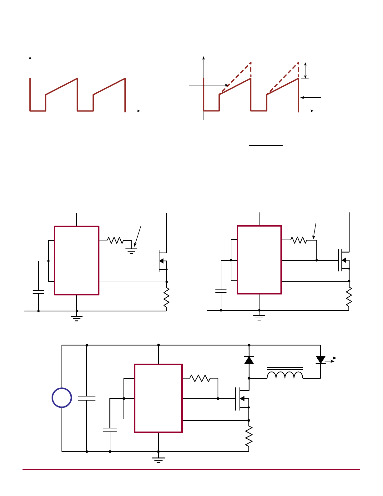
Fig. 2. Slope Compensation to Eliminate Subharmonic Oscillation
Slope Compensation
HV9910B
VIN
RT
GATE
CS
VDD
LD
PWMD
GND
C
2
R
1
R
2
Q1
Connected
to GATE
Connected
to GND
HV9910B
VIN
RT
GATE
CS
VDD
LD
PWMD
GND
C
2
R
2
Q1
AN-H50
I
R2
Current Through
Sense Resistor
Added
External Slope
t
The unique design of the oscillator in the HV9910B allows
the IC to be congured for either constant frequency or constant off-time based on how one resistor, connected to the
RT pin, is wired. For normal operation as constant frequency
converter, the resistor at the RT pin is connected to GND
(Fig. 3a). For operation as a constant off-time converter, the
resistor is connected between the RT and GATE pins (Fig.
3b). In both cases, the equation to determine the resistor is
Fig. 3a. Constant Frequency Operation
V
CS
Error due to
t
given by:
T
OSC
(µs) =
For constant frequency operation T
RT(kΩ) + 22
25
is set to the switching
OSC
time period and for constant off-time operation, T
the required off-time.
Fig. 3b. Constant Off-Time Operation
Voltage Across
Sense Resistor
is set to
OSC
Fig. 4 Circuit Diagram
LED(s)
D1
VIN
VDD
C
1
+
-
C
2
HV9910B
LD
PWMD
GND
RT
GATE
CS
R
1
L1
Q1
R
2
Supertex inc. ● 1235 Bordeaux Drive, Sunnyvale, CA 94089 ● Tel: 408-222-8888 ● www.supertex.com
2
Page 43

AN-H50
√
An example detailing the design of a constant off-time buck
converter is shown in Fig. 4.
Input Voltage:
V
V
V
IN,MIN
IN,NOM
IN,MAX
= 9V
= 12V
= 16V
Output Voltage (corresponds to two 1W LEDs):
V
V
V
O,MIN
O,NOM
O,MAX
= 4.6V
= 6.8V
= 8V
LED current:
IO = 350mA
Expected Efciency:
η = 0.85
Step 1: Choose the Nominal Switching Frequency
Although the switching frequency is variable, a nominal
switching frequency can be chosen. The actual frequency
will vary around this nominal value based on the actual input
and output conditions. A larger switching frequency will typically result in a smaller inductor, but will increase the switching losses in the circuit.
A typical switching frequency: f
= 100kHz is a good com-
S,NOM
promise, which corresponds to a time period of:
T
= 1 = 10μs (1)
S,NOM
f
S,NOM
Step 2: Compute the Off-Time and Resistor R1
The off-time can be calculated as:
V
(2)
t
OFF
=−
O,NOM
1
V
IN,NOM
x T
S,NOM
This off-time will then be set by the resistor R1 based on the
following equation:
R1 = (t
In this case, t
(μs) • 25) - 22 (kΩ) (3)
OFF
= 4.33μs and R1 = 86.25kΩ.
OFF
Note that in this case, the converter is operating at 56.7%
duty cycle.
Step 3: Choose the required Inductor L1
The value of the inductor L1 will depend on the peak-to-peak
ripple desired in the output current. Assuming a 30% peak to
peak ripple in the output current,
L1 =
O,NOM
OFF
0.3 • I
O
(4)
V
• t
The peak current rating of the inductor should be greater
than 1.3xIO and the rms current rating of the inductor should
be at least IO. For this example, the closest inductor avail-
able is a 330μH inductor with a 0.6A rms current rating and
a 0.6A saturation current rating.
Step 4: Choose the Sense Resistor (R2)
The peak current sensed by the HV9910 corresponds to the
average output current plus one half of the actual current
ripple. The peak current is given by:
IPK = IO +
O,NOM
OFF
2 • L1
(5)
V
• t
The sense resistor can be then be computed as:
R2 =
0.25
(6)
I
PK
if the internal voltage threshold is being used. Otherwise,
substitute the voltage at the LD pin instead of the 0.25V in
equation (6). The power rating required for the sense resistor can be computed using:
V
(7)
P
SENSE
= (IO)2 X
O,MAX
V
IN,MIN
R
× 2
For this design,
IPK = 0.394A, R2 = 0.633Ω, and P
= 0.069W
SENSE
Note: Capacitor C2 is a bypass capacitor. A typical value of
1μF, 16V ceramic capacitor is recommended.
Step 5: Choose the FET (Q1) and Diode (D1)
The peak voltage seen by the FET is equal to the maximum
input voltage. Using a 50% safety rating:
V
= 1.5 • V
FET
= 24V
IN,MAX
(8)
The maximum rms current through the FET is:
V
(9)
I
FET
= IO x
V
O,MAX
IN,MIN
Supertex inc. ● 1235 Bordeaux Drive, Sunnyvale, CA 94089 ● Tel: 408-222-8888 ● www.supertex.com
3
Page 44

Supertex inc.
94089
.supertex.com
AN-H50
V
10
V
Typically a FET with about 3 times the current is chosen to
minimize the resistive losses in the switch. For this applica-
tion, choose a 40V, 1Ω FET (TN2504 from Supertex in a
SOT-89 package).
The peak voltage rating of the diode is the same as the FET.
Hence:
V
DIODE
= V
= 24V
FET
(10)
The average current through the diode is:
V
(11)
I
DIODE
I
=×−
o
O,MIN
V
IN,MAX
A
25.
=
Choose a 30V, 1A schottky diode.
Step 6: Analysis of the Switching Frequency Variation
The two extremes of the switching frequency can be approximately computed as:
(12)
f
S,MIN
(13)
f
S,MAX
1
==
T
S,MAX
1
1
==
T
S,MIN
O,MAX
1
−
O,MIN
−
t
OFF
t
OFF
V
V
IN,MAX
IN,MIN
In this case, the switching frequency varies from:
25kHz (VIN = 9V, VO = 8V) to
164kHz (VIN = 16V, VO = 4.6V)
Supertex inc. does not recommend the use of its products in life support applications, and will not knowingly sell them for use in such applications unless it receives
an adequate “product liability indemnification insurance agreement.” Supertex inc. does not assume responsibility for use of devices described, and limits its liability
to the replacement of the devices determined defective due to workmanship. No responsibility is assumed for possible omissions and inaccuracies. Circuitry and
specifications are subject to change without notice. For the latest product specifications refer to the Supertex inc. (website: http//www.supertex.com)
©2011 Supertex inc. All rights reserved. Unauthorized use or reproduction is prohibited.
1110 11
1235 Bordeaux Drive, Sunnyvale, CA
4
Tel: 408-222-8888
www
Page 45
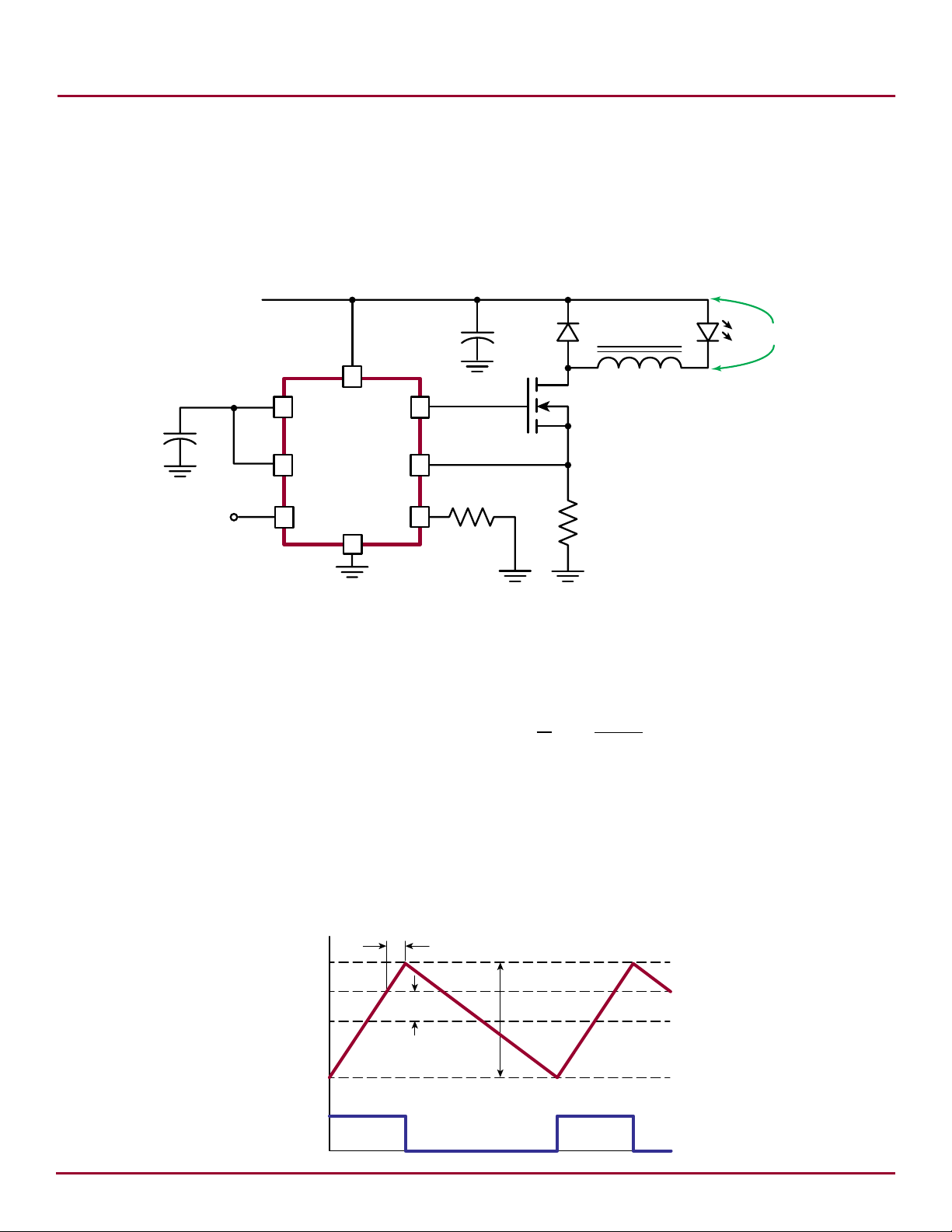
Supertex inc.
Compatibility and Functional Differences between
the HV9961 and HV9910B LED Drivers
Figure 1. Typical application circuit of HV9910B and HV9961.
V
IN
AN-H64
Application Note
V
O
1
PWMD
VIN
GATE
4
5
HV9961
6
VDD
or
CS
2
HV9910B
V
LD
7
LD
GND
3
RT
8
R
T
Peak-Current Control vs. Average-Mode
Current Control
Peak-current control of a buck converter used in the
HV9910B, while being the most economical and simplest way
to regulate the LED current, suffers accuracy and regulation
problems. These problems arise from the so-called peak-toaverage current error, contributed by the current ripple in the
output inductor and by the propagation delay in the current
sense comparator.
The peak-to-average current error ∆I
HV9910B, since the IC is controlling the peak inductor cur-
is inherent to the
L(ERR)
L
R
CS
rent I
rent I
one-half of the inductor current ripple ∆IL, which can be ex-
pressed by the following equation:
In this equation, VO is the LED voltage, t
of the GATE output of the HV9910B (the lower waveform in
Fig.2), and L is the inductance value. Note that all parameters in right side of Equation 1 can vary from one part to
another and depend on the operating temperature.
, whereas the intent is to regulate the average cur-
L(PK)
. The difference between the two currents equals
L(AVG)
1
2
∆IL =
VOt
OFF
(1)
2L
is the off-time
OFF
Figure 2. Peak-to-average current error produced by the peak-current control method of
HV9910B.
Δt
L(ERR)
CS
ΔI
L
OFF ON
I
L(PK)
I
L(CS)
I
L(AVG)
ΔI
ON
Supertex inc. ● 1235 Bordeaux Drive, Sunnyvale, CA 94089 ● Tel: 408-222-8888 ● www.supertex.com
Page 46
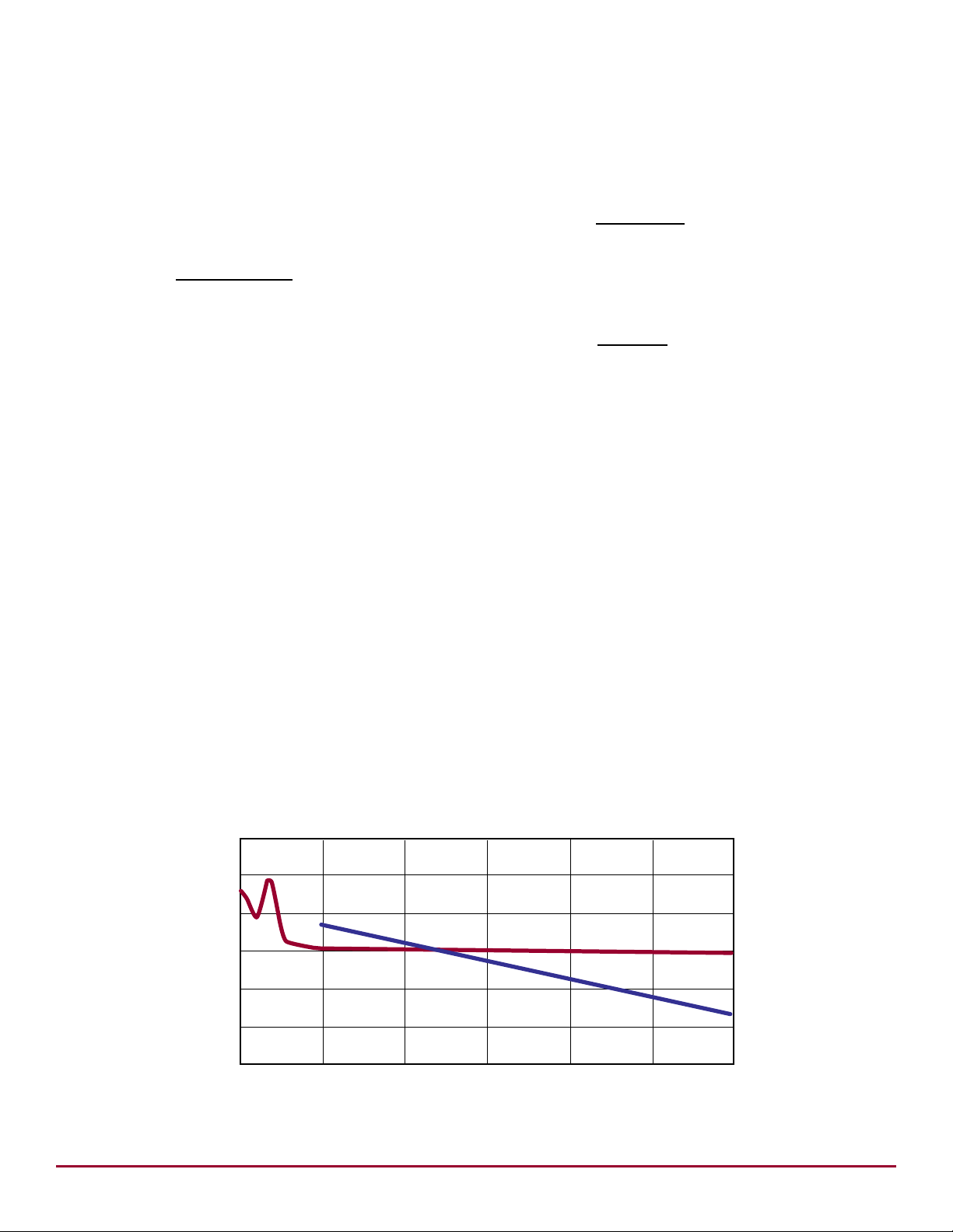
AN-H64
Another source of error produced by a peak-current controller such as the HV9910B is associated with the current-
sense comparator delay ∆tCS. The actual peak current I
is higher than the comparator threshold reference I
L(CS)
L(PK)
because of this propagation delay. Therefore, the total peak-toaverage error can be expressed as:
∆I
L(ERR)
=
VOt
- 2VIN∆t
OFF
2L
CS
(2)
where VIN is the input DC power supply voltage.
As one could see from Equation 2, the average inductor cur-
rent I
also suffers poor load and line regulation, since it
L(AVG)
is dependent on the input voltage VIN and the output voltage
VO.
Lastly, there is a signicant part-to-part variation in the LED
current that occurs due to the CS input offset voltage VOS.
Although this offset voltage is only ±25mV at -40°C < TA
< +85°C, it contributes as much as ±10% variation of the
LED current even at the maximum CS threshold voltage of
250mV.
The HV9961 overcomes the above drawbacks by means of
Supertex’s average-mode constant current control method.
The IC regulates the average inductor current I
L(AVG)
direct-
ly and accurately within ±3% over a wide GATE duty cycle
range of at least 0.1 < D < 0.75. It also includes an auto-zero
circuit at the CS input that cancels the propagation and off-
set errors.
Linear Dimming
When the LD voltage is VLD ≥1.5V, the output LED current is
simply programmed with the HV9961 as:
I
L(AVG)
where 272mV is the internally xed reference voltage. Otherwise:
I
L(AVG)
Unlike the HV9910B, which has the LD range from 0 to 0.25V,
the active LD input voltage range of the HV9961 is from 0
to 1.5V. Moreover, for the HV9910B, V
produce I
LED
some residual LED current remaining despite connecting LD
to GND. The HV9961 overcomes this issue by disabling the
GATE output when V
sumes when V
Note that the latter feature of the HV9961 allows a mixedmode PWM/linear dimming mode. A single square-wave input signal can be applied at LD, where both the signal duty
cycle and its amplitude are modulated in order to expand the
dimming range.
272mV ±3%
=
R
(3)
CS
VLD ±3%
=
5.5 • R
(4)
CS
= 0A due to the D
< 150mV. The GATE switching re-
LD
> 200mV.
LD
= GND does not
limitation. There is always
MIN
LD
Figure 3. Typical output voltage regulation characteristic of LED current.
0.50
0.45
0.40
HV9961
0.35
0.30
LED Current (A)
0.25
0.20
0 10 20 30 40 50 60
HV9910B
Output Voltage (V)
Supertex inc. ● 1235 Bordeaux Drive, Sunnyvale, CA 94089 ● Tel: 408-222-8888 ● www.supertex.com
2
Page 47
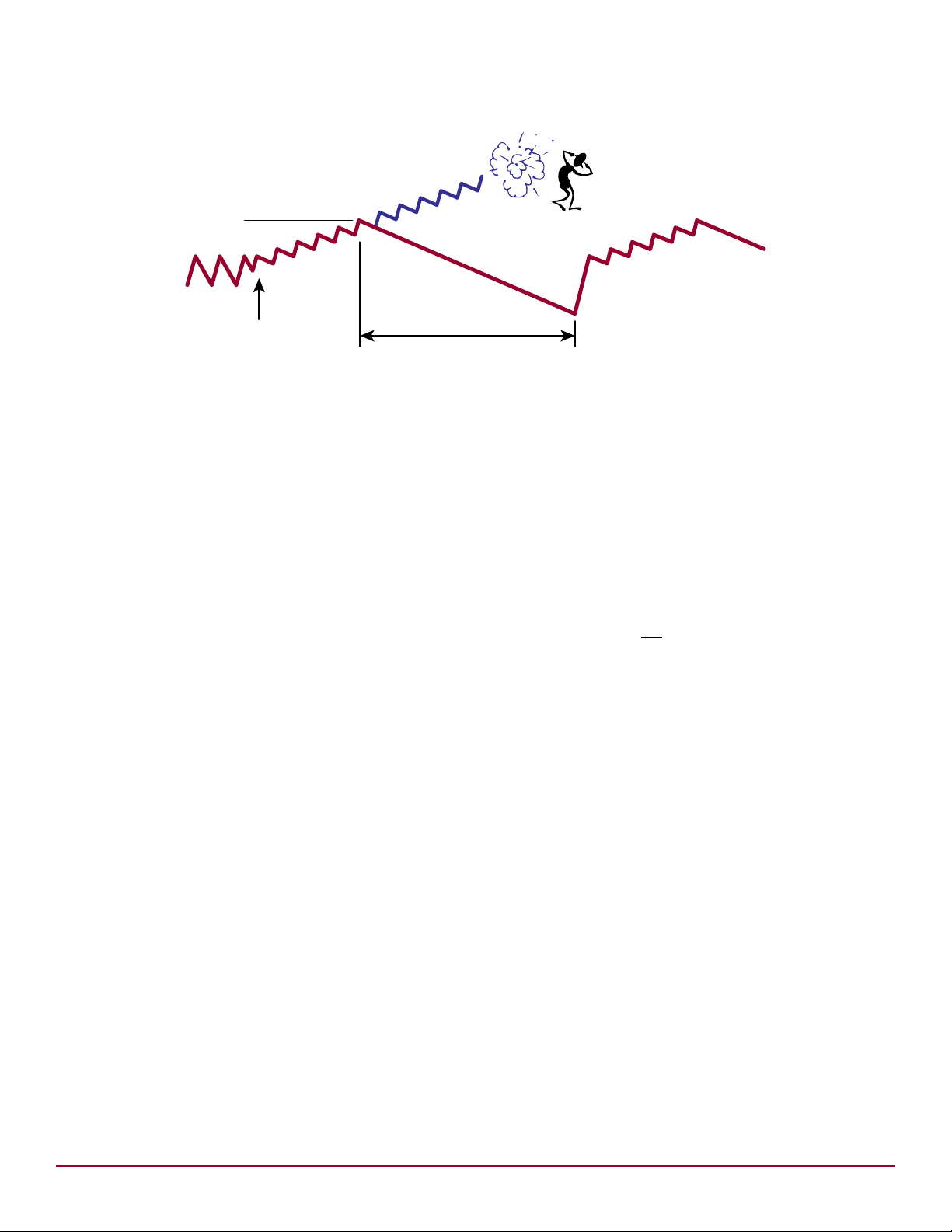
(
(
Figure 4. Effect of the output short circuit on the inductor current.
HV9910B
I
LIM
AN-H64
HV9961
SHORT
400µs
Short-Circuit Protection
Both the HV9910B and HV9961 are characterized by a min-
imum on-time of the GATE output. This minimum on-time
includes the leading-edge blanking delay and the currentsense comparator propagation delay. The minimum on-
time is 0.47µs(max) for the HV9910B and 1.0µs(max) for
the HV9961. When a short circuit is applied at the output of
the buck converter, the only voltage available to reset the
magnetic ux in the inductor during t
is the rectier di-
OFF
ode voltage drop. When the converter keeps switching at
the same frequency rate this may not be enough. Therefore,
the inductor current will keep rising every switching cycle.
(See Figure 4.)
The HV9961 is protecting the LED driver from such “staircase” saturation of the inductor by introducing a second
threshold I
= 0.44V/RCS. When this threshold is reached,
LIM
the GATE output becomes disabled for 400µs, thus letting
the inductor current ramp down to a safe level.
Constant-Frequency and Constant Off-Time
Operating Modes
The HV9910B can be congured for operating in either
switching mode. When RT is connected to GND, it maintains
a constant switching frequency. Wiring RT to GATE yields a
xed t
t
t
where t
t
OFF
The HV9961 does not support the xed frequency mode.
Moreover, the RT resistor must be wired to GND in all cases.
mode. The corresponding timing equations are:
OFF
= 40pF • RT + 0.88µs (5a)
OSC
= 40pF • RT + 0.88µs (5b)
OFF
is the switching period with RT wired to GND, and
OSC
is the off-time with RT connected to GATE.
Therefore, the HV9961 cannot be used as a direct drop-in
replacement in the applications of the HV9910B wired for
the xed t
HV9961 t
t
operation, and a layout change is required. The
OFF
is given by:
OFF
= 40pF • RT + 0.3µs (5c)
OFF
If the HV9910B is wired for the xed frequency operation,
the conversion to the HV9961 will merely require the RT re-
sistor value change. Since t
= (1-VO / VIN) • t
OFF
, Equations
OSC
5a and 5c can be solved for the new RT value:
V
R
T(HV9961)
= 1 -
O
• (R
V
IN
T(HV9910B)
+ 22kΩ) - 7.5kΩ (6)
Duty Cycle Range
The duty cycle is determined by the equation D = tON/t
= tON/(t
their minimum duty cycle D
+ tON). Both the HV9910B and the HV9961 have
OFF
limited by the minimum on-
min
time. However, with the HV9961 the guaranteed ±3% accuracy of the LED current can only be achieved with the duty
cycle D
>0.08~0.1.
min
The maximum duty cycle of the HV9910B operating with
the xed frequency is limited to D
= 0.5. Exceeding D =
max
0.5 with this operating mode causes sub-harmonic oscillation at ½ of the switching frequency. When the HV9910B is
operated with xed t
, there is no theoretical limit of D
OFF
However, due to parasitic resistances in the circuit and large
switching frequency variation, it is not recommended that a
D
= 0.8 be exceeded with this operating mode.
max
With the HV9961, regulation of the average inductor current
is limited to D
≤ 0.75. When D = 0.75 (125oC) or D = 0.8
max
(105oC) is exceeded, the functionality of the HV9961 will begin approaching that of the HV9910B, and the LED current
will drop accordingly.
OSC
max
.
Supertex inc. ● 1235 Bordeaux Drive, Sunnyvale, CA 94089 ● Tel: 408-222-8888 ● www.supertex.com
3
Page 48

Supertex inc.
94089
.supertex.com
Table 1. Functional comparison of HV9910B and HV9961.
Feature HV9910B HV9961
Fixed-Frequency Mode Resistor from RT to GND N/A
Resistor from RT to GND
Fixed Off-Time Mode Resistor from RT to GATE
(value adjustment needed for
conversion from HV9910B)
AN-H64
Current Threshold 250mV or V
(peak) 272mV or V
LD
/5.5 (average)
LD
Current Threshold Accuracy 10% Auto-zero
LED Current Accuracy
LED Current Regulation
Depends on inductance and
switching frequency variation
Poor. LED current depends on input
and output voltage
Independent of inductance and
switching frequency variation
Good
LD Input Range 0 to 250mV 0.2V(0.15V) to 1.5V
Residual LED Current at V
= GND 5% (typ.) of I
LD
LED
@ V
= 250mV 0A
LD
Current Limit Threshold none 440mV
Hiccup Time N/A 400µs
Minimum On-Time 465ns 1000ns
Maximum Duty Cycle 0.5 (xed freq.), 0.8 (xed T
) 0.75
OFF
Supertex inc. does not recommend the use of its products in life support applications, and will not knowingly sell them for use in such applications unless it receives
an adequate “product liability indemnification insurance agreement.” Supertex inc. does not assume responsibility for use of devices described, and limits its liability
to the replacement of the devices determined defective due to workmanship. No responsibility is assumed for possible omissions and inaccuracies. Circuitry and
specifications are subject to change without notice. For the latest product specifications refer to the Supertex inc. (website: http//www.supertex.com)
©2011 Supertex inc. All rights reserved. Unauthorized use or reproduction is prohibited.
081109
1235 Bordeaux Drive, Sunnyvale, CA
4
Tel: 408-222-8888
www
Page 49
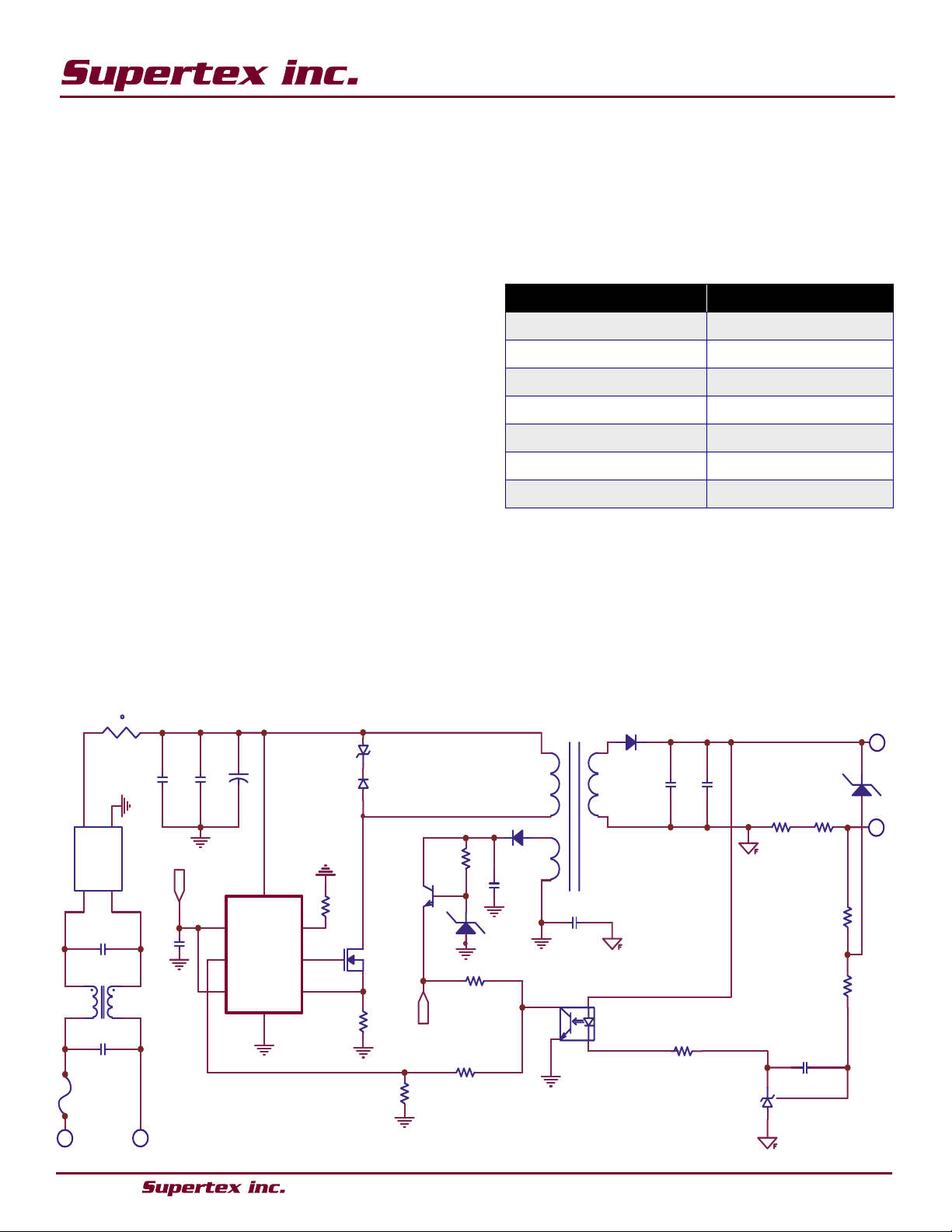
● 1235 Bordeaux Drive, Sunnyvale, CA 94089 ● Tel: 408-222-8888 ● www.supertex.com
Isolated LED Driver
C
3
10uF, 400V
C
2
2.2uF , 400V
1
2
3
4
L
1
BU9H S-153R15B
C
4
0
.
0
1
u
F
,
2
5
0
V
A
C
C
1
0.0
1
u
F
,
2
5
0
V
A
C
F
1
2
A
,25
0
V
A
C
1
3
2
D
9
L
M
V
4
3
1
D
7
9.1
V
C
1
2
1
n
,
2
5
0
V
A
C
D
2
B
1
1
0
0
-
1
3
D
4
B
A
V
2
0
W
-
7
Q
3
S
T
D
1
N
K
6
0
T
4
R
8
0
.56
VIN
1
LD
1
3
PW
MD
9
GND
5
C
S
4
GATE
8
RT
1
4
VDD
1
2
U
2
C
9
1uF, 16V
V
DD
V
DD
C
8
1uF, 50V
D
1
1
N
4
7
6
4
A
D
O
4
1
D
3
M
U
R
1
4
0
R
L
R
5
2
2
8
k
C
5
4.7uF , 25V
C
6
4.7uF , 25V
L
E
D
+
1
L
E
D
-
1
R
2
1
.
7
8
,
1
/
4
W
R
1
1
.
7
8
,1
/
4
W
R
7
2
0
k
C
1
1
0
.1u
F
R
9
1
k
U
3
H
1
1
A
8
17A
R
1
3
1
0
0
D
8
2
0
V
R
6
5.49k
R
1
1
97.
6
k
R
1
2
4
.
9
9
k
R
3
1
k
Q
1
M
M
B
T
2
2
2
2
A
t
R
T
1
C
L
-
1
4
0
C
1
3
2.2uF , 400V
1
3
9
1
0
4
5
O
O
O
T
1
J
1
J
2
AC1
AC2
POS
NEG
U
1
HV9910B
Using the HV9910B
DN-H01
Design Note
Introduction
In a few general lighting applications, there is a need to isolate
the LEDs from the AC input line. These are cases when
the driver terminals of the LED strings are exposed to the
external environmental conditions, or the LED strings are user
accessible for maintenance during operation. In these cases,
an isolated LED driver is needed for safety considerations.
This design note provides the circuit schematic, bill of
materials, and transformer design for an isolated LED driver
using Supertex’s HV9910B. The power stage is a flyback
converter with an isolated secondary side feedback, using an
opto coupler, to ensure a very good line and load regulation
(typically <1% over line and load). Below are the design
parameters which are the target specification for this LED
driver circuit. This LED driver will also meet CISPR-15 EMI
limits for general lighting.
The information in this datasheet also applies to the Supertex
HV9910.
Circuit Schematic
Design Parameters
Parameter Value
Input voltage 90 – 256VAC, 50/60Hz
LED string voltage 4.0 – 16V
LED current 350mA
Initial regulation <5%
Line and load regulation <1%
Over voltage protection 20V
Switching Frequency 100kHz
Page 50
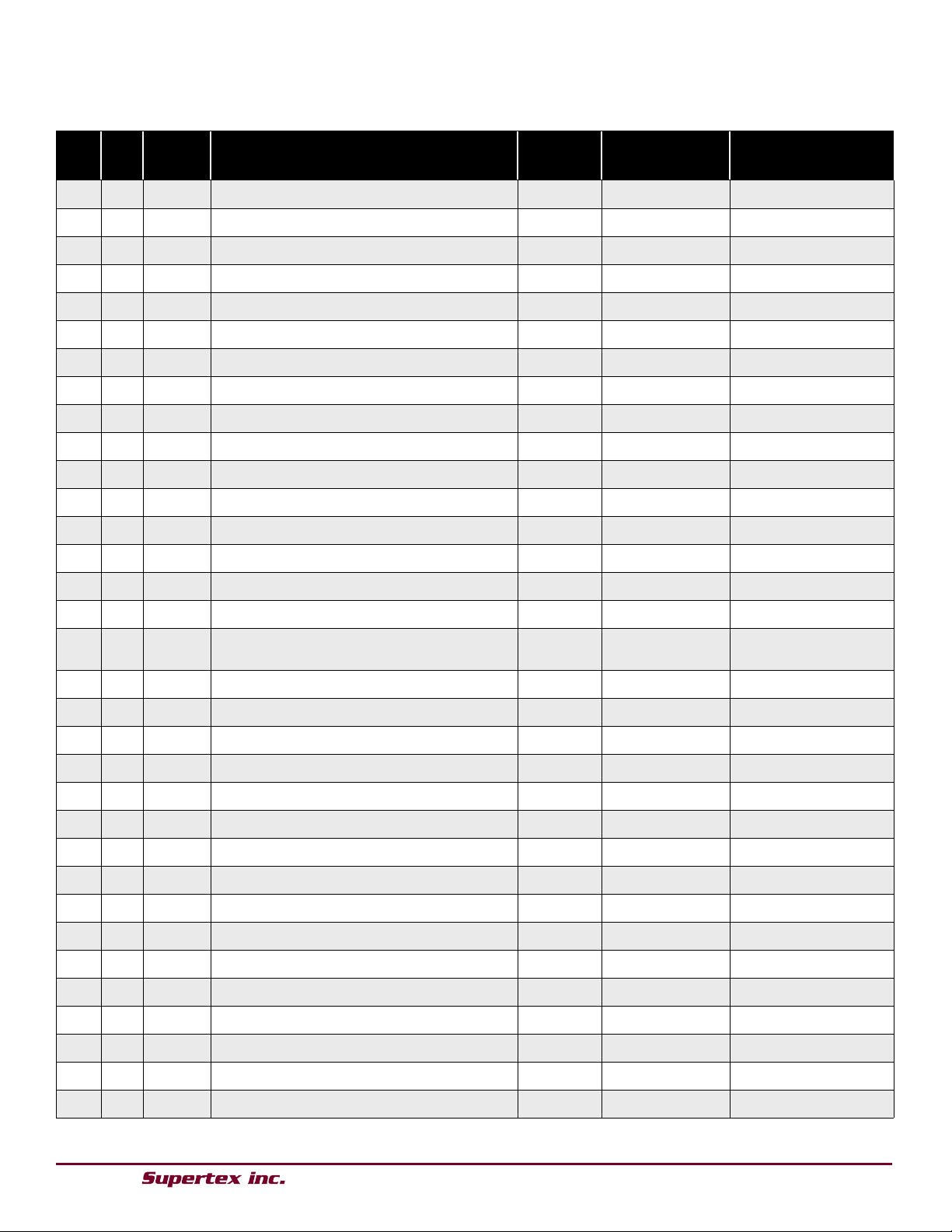
● 1235 Bordeaux Drive, Sunnyvale, CA 94089 ● Tel: 408-222-8888 ● www.supertex.com
Bill of Materials
DN-H01
Item
Qty Ref Description Package Manufacturer
#
1 2 C1, C4 0.01uF, 250VAC metal polypropylene capacitors Thru-Hole EPCOS Inc B81122A1103M
2 2 C2, C13 2.2uF, 400V metal film capacitors Thru-Hole Panasonic ECQ-E4225KF
3 1 C3 10uF, 400V electrolytic capacitors Radial Nichion UVR2G100MHD
4 2 C5, C6 4.7uF, 25V X7R ceramic chip capacitor SMD1210 TDK Corporation C3225X7R1E475M
5 1 C8 1uF, 50V X7R ceramic chip capacitor SMD1206 TDK Corporation C3216X7R1H105K
6 1 C9 1uF, 16V X7R ceramic chip capacitor SMD0805 TDK Corporation C2012X7R1C105K
7 1 C11 0.1uF, 16V X7R ceramic chip capacitor SMD0805 Kemet C0805C104K4RACTU
8 1 C12 1n, 250VAC ceramic capacitor Y2/X1 Thru-Hole Panasonic ECK-NVS102ME
9 1 D1 100V, 1W zener diode DO-41 Micro Semi 1N4764ADO41
10 1 D2 100V, 1A schottky diode SMA Diodes Inc B1100-13
11 1 D3 400V, 1A ultrafast switching diode DO-41 On Semi MUR140RL
12 2 D4 150V, 400mA switching diode SOD123 Diodes Inc BAV20W-7
13 1 D7 9.1V, 500mW zener diode SOD123 Diodes Inc BZT52C9V1-7
14 1 D8 20V, 500mW zener diode SOD123 Diodes Inc BZT52C20-7-F
15 1 D9 1.24V, precision shunt regulator SOT-23 National Semi LMV431
Manufacturer’s Part
Number
16 1 F1 2A, 250VAC fuse Thru-Hole Cooper/Bussmann BK/PCB-2
17 1 L1
18 1 Q1 40V, 600mA NPN transistor SOT-23 ST Micro MMBT2222A
19 1 Q3 600V, 1A N-Channel MOSFET DPAK ST Micro STD1NK60T4
20 1 RT1 50ohm Inrush current limiter Thru-Hole GE Infrastructure CL-140
21 2 R1, R2 1.78,1/4W, 1% chip resistor SMD0805 Yageo 9C12063A1R78FGHFT
22 2 R3, R9 1k, 1/8W, 1% chip resistor SMD0805 Yageo 9C08052A1001FKHFT
23 1 R5 226k, 1/8W, 1% chip resistor SMD0805 Yageo 9C08052A2263FKHFT
24 1 R6 5.49k, 1/8W, 1% chip resistor SMD0805 Yageo 9C08052A5491FKHFT
25 1 R7 20k, 1/8W, 1% chip resistor SMD0805 Yageo 9C08052A2002FKHFT
26 1 R8 0.56, 1/8W, 1% chip resistor SMD0805 Panasonic ERJ-6RQFR56V
27 1 R11 97.6k, 1/8W, 1% chip resistor SMD0805 Yageo 9C08052A9762FKHFT
28 1 R12 4.99k, 1/8W, 1% chip resistor SMD0805 Yageo 9C08052A4991FKHFT
29 1 R13 100 ohm, 1/8W, 1% chip resistor SMD0805 Yageo 9C08052A1000FKHFT
30 1 T1 Flyback Transformer - - ---
31 1 U1 400V, 1A Single Phase diode bridge rectifier DF-S Diodes Inc DF04S
15mH (300uH differential),
0.15A rms common mode choke
Thru-Hole Coilcraft BU9HS-153R15B
32 1 U2 Universal LED Driver SO-16 Supertex HV9910BNG-G
33 1 U3 Single Channel Optoisolator 4-DIP Fairchild H11A817A
2
Page 51
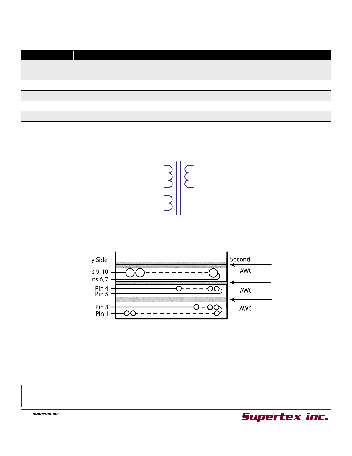
Supertex inc. does not recommend the use of its products in life support applications, and will not knowingly sell them for use in such applications unless it receives an
adequate “product liability indemnification insurance agreement.” Supertex inc. does not assume responsibility for use of devices described, and limits its liability to the
replacement of the devices determined defective due to workmanship. No responsibility is assumed for possible omissions and inaccuracies. Circuitry and specifications
are subject to change without notice. For the latest product specifications refer to the Supertex inc. website: http//www.supertex.com
.
©2009 All rights reserved. Unauthorized use or reproduction is prohibited .
1235 Bordeaux Drive, Sunnyvale, CA 94089
Tel: 408-222-8888
www.supertex.com
Flyback Transformer Details
Primary
Auxiliar
y
Secondary
1
3
9
10
4
5
O
O
O
T1
Pin 1
Pin
3
Pin 5
Pin 4
Pins 6, 7
Pins 9,
10
Pr
imary Side
Secondary Side
AWG #24
AW
G #32
AW
G #32
2 Layers Tape
2 Layers Tape
2 Layers Tape
Component Description
DN-H01
Core :
EFD20/10/7 – 3C90 – A250 from Ferroxcube
(EFD 20 core with 160µm gap in the center leg)
Bobbin: CPHS – EFD20 – 1S – 10P from Ferroxcube
Primary: 66 turns of AWG#32 magnet wire
Secondary: 13 turns of AWG#24 equivalent triple-insulated litz wire
Auxiliary: 32 turns of AWG#32 magnet wire
Insulation: 3M 1928 Polyester Film, 2.0 mil thick tape
Schematic Diagram of the Transformer
L
= 1.1mH ± 8%
PRIMARY
Leakage inductance = 8% of L
PRIMARY
Winding Diagram
022009
3
Page 52
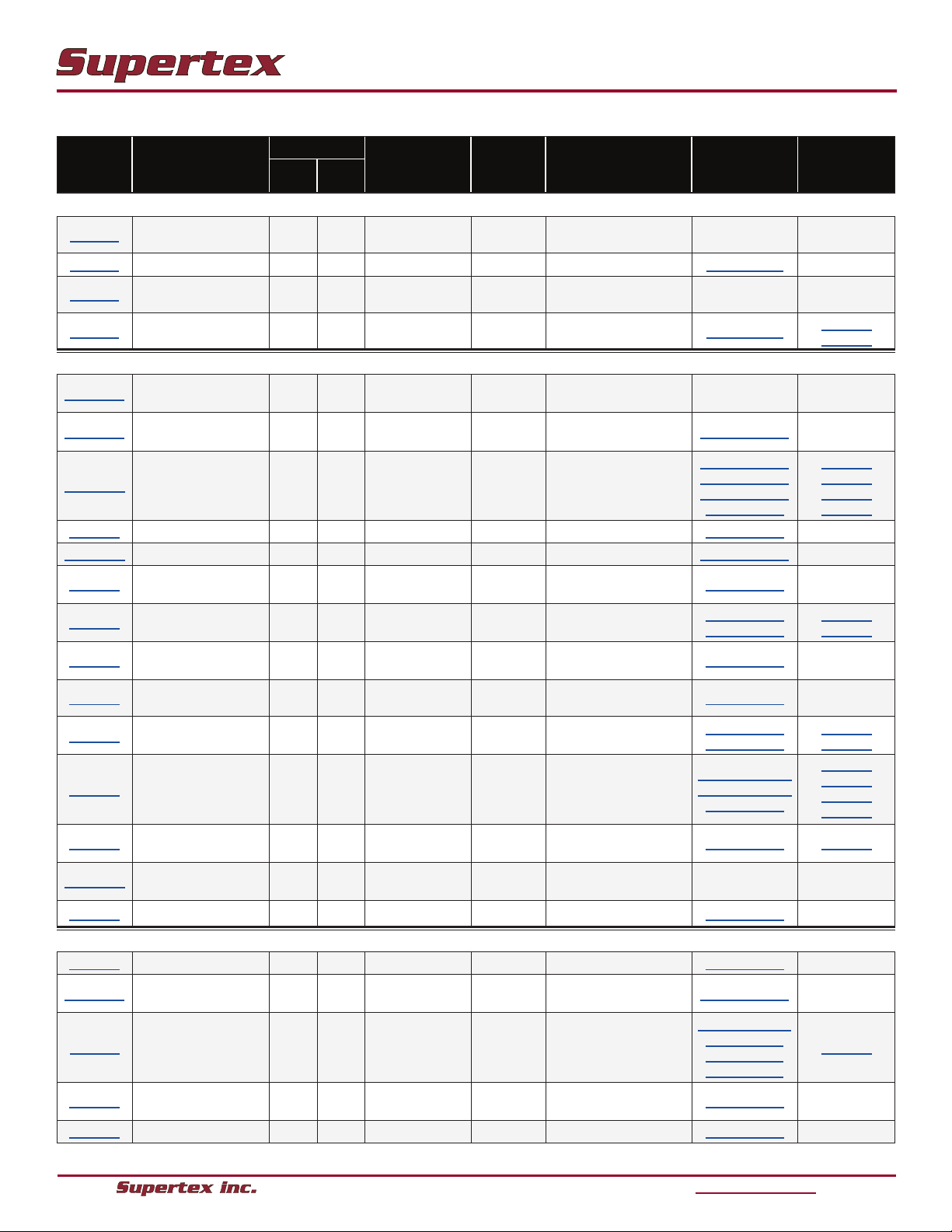
Selector Guide
Switching Converters
Device Topology
min
(V)
V
IN
max
(V)
LED Driver ICs
Output
Current
(mA)
Dimming
Package
Options
Demoboards
Application/
Design
Notes
Automotive (AEC-Q100 Certied) LED Drivers
AT9917 Boost, SEPIC 5.3 40 External FET
AT9919 Buck 4.5 40 External FET PWM 8-Lead DFN (K7) AT9919DB1 ---
AT9932 Boost-Buck (Ćuk) 5.3 40 External FET
AT9933 Boost-Buck (Ćuk) 9.0 75 External FET PWM 8-Lead SOIC (LG) AT9933DB1
PWM /
Linear
PWM /
Linear
24-Lead TSSOP (TS) --- ---
24-Lead TSSOP (TS) --- ---
AN-H51
AN-H58
General Purpose LED Drivers
HV9801A Buck 15 450 External FET
HV9861A Buck 12 450 External FET
HV9910B Buck 8.0 450 External FET
HV9918 Buck 4.5 40 Integrated FET PWM 8-Lead DFN (K7) HV9918DB1 ---
HV9919B Buck 4.5 40 External FET PWM 8-Lead DFN (K7) HV9919BDB1 ---
HV9921 Buck 20 400 20 No
HV9922 Buck 20 400 50 No
HV9923 Buck 20 400 30 No
HV9925 Buck 20 400 20 - 50 PWM
HV9930 Hysteric 8.0 200 External FET PWM 8-Lead SOIC (LG)
HV9931 Single-Switch PFC 8.0 450 External FET PWM 8-Lead SOIC (LG)
HV9961 Buck 8.0 450 External FET
HV9967B Buck 8.0 60 External FET
HV9971 Flyback - - External FET PWM 8-Lead SOIC (LG) HV9971DB1 ---
4-Level
Switch
PWM /
Linear
PWM /
Linear
PWM /
Linear
PWM /
Linear
8-Lead SOIC (LG)
16-Lead SOIC (NG)
8-Lead SOIC (LG)
16-Lead SOIC (NG)
8-Lead SOIC (LG)
16-Lead SOIC (NG)
3-Lead TO-92 (N3)
3-Lead SOT-89 (N8)
3-Lead TO-92 (N3)
3-Lead SOT-89 (N8)
3-Lead TO-92 (N3)
3-Lead SOT-89 (N8)
8-Lead SOIC (SG)
w/ Heat Slug
8-Lead SOIC (LG)
16-Lead SOIC (NG)
8-Lead DFN (K7)
8-Lead MSOP (MG)
--- ---
HV9861ADB1 ---
HV9910BDB2
HV9910BDB3
HV9910BDB7
HV9910DB6
HV9921DB1 ---
HV9922DB1
HV9922DB2
HV9923DB1 ---
HV9925DB1 ---
HV9930DB1
HV9930DB2
HV9931DB1v2
HV9931DB2v1
HV9931DB5
HV9961DB1 AN-H64
--- ---
AN-H48
AN-H50
AN-H64
DN-H01
DN-H02
DN-H03
AN-H51
AN-H58
AN-H52
DN-H04
DN-H05
DN-H06
Backlight LED Drivers
HV9860 Boost 10 40 External FET PWM 16-Lead SOIC (NG) HV9860DB1 ---
HV9861A
HV9911
HV9912
HV9957 Boost 2.7 28 30 x 6-Channel PWM 24-Lead QFN (K7) HV9957DB1 ---
● 1235 Bordeaux Drive, Sunnyvale, CA 94089 ● Tel: (408) 222-8888 ●
Buck
Boost, SEPIC,
Buck-Boost
Boost, SEPIC,
Buck-Boost
12 450 External FET
9.0 250 External FET PWM 16-Lead SOIC (NG)
9.0 100 External FET PWM 16-Lead SOIC (NG)
PWM /
Linear
8-Lead SOIC (LG)
16-Lead SOIC (NG)
HV9861ADB1 ---
HV9911DB1v2
HV9911DB2
HV9911DB3
HV9911DB4
HV9912DB1 ---
www.supertex.com
AN-H55
Page 53
Selector Guide
Switching Converters
Device Topology
min
(V)
V
IN
max
(V)
LED Driver ICs
Output
Current
(mA)
Dimming
Package
Options
Backlight LED Drivers (cont.)
HV9961 Buck 8.0 450 External FET
HV9963
Boost, SEPIC,
Buck-Boost
8.0 40 External FET
HV9967B Buck 8.0 60 External FET
HV9980 Buck 100 160 70
HV9982 Boost, SEPIC 10 40 External FET
HV9985 Boost, SEPIC 10 40 External FET
HV9986 Boost, SEPIC 10 40 External FET
HV9989 Boost, SEPIC 10 40 External FET
PWM /
Linear
PWM /
Linear
PWM /
Linear
PWM /
Linear
PWM /
Linear
PWM /
Linear
PWM /
Linear
PWM /
Linear
8-Lead SOIC (LG)
16-Lead SOIC (NG)
16-Lead SOIC (NG) --- ---
8-Lead DFN (K7)
8-Lead MSOP (MG)
24-Lead SOW (WG) HV9980DB1 ---
40-Lead QFN (K6) HV9982DB1 ---
40-Lead QFN (K6)
44-Lead QSOP (QP)
40-Lead QFN (K6) --- ---
40-Lead QFN (K6) --- ---
Ofine PFC
HV9931 Buck, BIBRED 8.0 450 External FET PWM 8-Lead SOIC (LG)
Demoboards
Design
Notes
HV9961DB1 AN-H64
--- ---
HV9985DB1 ---
Application/
HV9931DB1v2
HV9931DB2v1
HV9931DB5
AN-H52
DN-H04
DN-H05
DN-H06
Linear Regulators
V
Device
CL2
CL25
CL220
CL320
CL325
CL330
CL520
CL525
CL6
CL7
IN
(V)
max
(V)
min
5.0 90 5.0 90 20
5.0 90 5.0 90 25
5.0 220 5.0 220 20
6.5 90 4.0 90 20
6.5 90 4.0 90 25
6.5 90 4.0 90 30
4.75 90 1.0 90 20 - Yes
4.75 90 1.0 90 25 - Yes
6.5 90 4.0 90 100 No Ye s
6.5 90 4.0 90 100
min
(V)
V
OUT
max
(V)
Output
Current
(mA)
Dimming Parallelable
External
FET
External
FET
External
FET
PWM
PWM
PWM
PWM
Yes
Yes
Yes
Yes
Yes
Yes
Yes
Package
Options
3-Lead TO-252 (K4)
3-Lead TO-92 (N3)
3-Lead SOT-89 (N8)
3-Lead TO-92 (N3)
3-Lead SOT-89 (N8)
3-Lead TO-252 (K4)
3-Lead TO-220 (N5)
8-Lead SOIC (SG)
w/ Heat Slug
8-Lead SOIC (SG)
w/ Heat Slug
8-Lead SOIC (SG)
w/ Heat Slug
3-Lead TO-252 (K4)
3-Lead TO-92 (N3)
3-Lead TO-252 (K4)
3-Lead TO-92 (N3)
3-Lead TO-252 (K4)
3-Lead TO-220 (N5)
8-Lead SOIC (SG)
w/ Heat Slug
Features
---
---
---
OTP, separate ENABLE pin
OTP, separate ENABLE pin
OTP, separate ENABLE pin
---
---
Reverse polarity protection, OTP
Reverse polarity protection, OTP
● 1235 Bordeaux Drive, Sunnyvale, CA 94089 ● Tel: (408) 222-8888 ●
www.supertex.com
 Loading...