

Page 1
查询HV508供应商
High Voltage Liquid Crystal
Shutter Driver
Ordering Information
Device HVIN Maximum Voltage Package Options
HV508 45V HV508LG
HV508
SO-8
Features
❏ HVCMOS technology for high performance
❏ Logic-selectable output voltage
❏ 100nF drive capability
❏ Up to 90V
❏ 25µs response time
P-P
General Description
The Supertex HV508 is a 45V liquid crystal shutter driver in an SO8 surface mount package. It consist of two outputs that provide
square waves of opposite phase. The liquid crystal shutter is
connected between the two outputs. Its equivalent load can be
approximated as a resistor in parallel with a capacitor. Minimum
resistance is 1.0MΩ and maximum capacitance is 0.1µF.
The HV508 has three input supply voltages, HV
The output’s amplitude will be either LVIN or HVIN. A logic high on
the HVEN input will set the output to operate from the HVIN supply.
A logic low on the HV
LVIN supply. The output frequency is set by the logic input frequency applied on the POL input.
input will set the output to operate from the
EN
, LVIN, and VDD.
IN
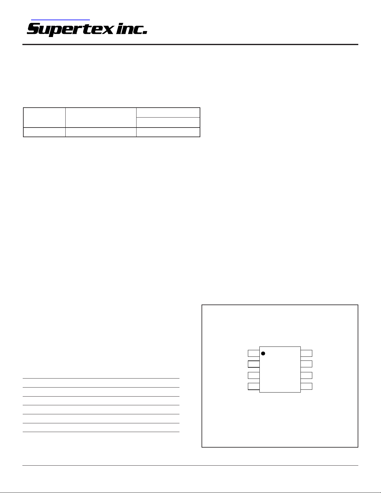
Pin Configuration
LV
Absolute Maximum* Ratings
HVIN, high voltage input +60V
LVIN, low voltage input +7.5V
VDD, logic supply voltage +12V
Continuous total power dissipation 700mW
Operating temperature -5°C to +60°C
Storage temperature –65°C to +150°C
Soldering temperature +300°C
* All voltages are referenced to GND.
For operation above 25°C ambient derate linearly at 6mW/°C.
12/13/01
Supertex Inc. does not recommend the use of its products in life support applications and will not knowingly sell its products for use in such applications unless it receives an adequate "products liability
indemnification insurance agreement." Supertex does not assume responsibility for use of devices described and limits its liability to the replacement of devices determined to be defective due to
workmanship. No responsibility is assumed for possible omissions or inaccuracies. Circuitry and specifications are subject to change without notice. For the latest product specifications, refer to the
Supertex website: http://www.supertex.com. For complete liability information on all Supertex products, refer to the most current databook or to the Legal/Disclaimer page on the Supertex website.
1
POL HV
HV
GND HV
EN
1
IN
2
3
4
top view
SO-8
HV
8
7
6
5
OUT1
IN
V
DD
OUT2
Page 2
Electrical Characteristics
HV508
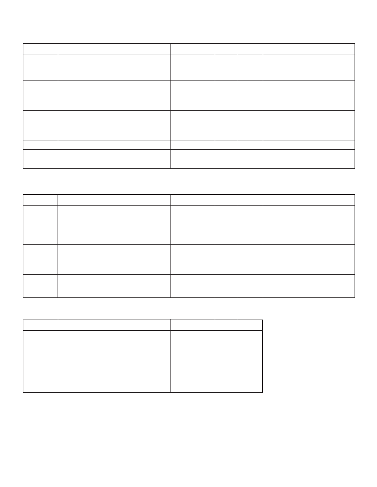
DC Electrical Characteristics (over operating supply voltages unless otherwise specified, T
= -5°C to +60°C)
A
Symbol Parameter Min Typ Max Unit Conditions
I
I
I
I
HVQ
LVQ
DDQ
HV
HVIN quiescent current 10 µA
LVIN quiescent current 10 µA
VDD quiescent current 10 µA
HVIN operating current 2.8 mA POL = 100Hz, HVEN = high,
= 25°C, Load = 1MΩ in parallel
T
A
with 0.1µF between HV
HV
OUT2
I
LV
LVIN operating current 380 µA POL = 100Hz, HVEN = low,
T
= 25°C, Load = 1MΩ in parallel
A
with 0.1µF between HV
HV
OUT2
I
IL
I
IH
C
LOAD
*The device can operate continuously without any damage within this range. AC limits are not implemented.
AC Electrical Characteristics (HV
Logic input current low -5 µA
Logic input current high 5.0 µA
Output capacitive load* 0 0.25 µFC
= 45V, LVIN = 6V, VDD = 5V, TA = -5°C to +60°C)
IN
LOAD
in parallel with a 1MΩ resistor
Symbol Parameter Min Typ Max Unit Conditions
f
POL
t
HV(ON)
t
HV(OFF)
POL input frequency 0 100 Hz
Turn-on time when high voltage is enable 16 µs Load = 1MΩ in parallel with 0.1µF
between HV
OUT1
Turn-off time when high voltage is enabled 16 µsHVEN = High. Outputs rise to HVIN.
See Fig. 1.
t
LV(ON)
t
LV(OFF)
Turn-on time when high voltage is disabled 40 µs Load = 1MΩ in parallel with 0.1µF
between HV
OUT1
Turn-off time when high voltage is disabled 6.0 µsHVEN = Low. Outputs rise to LVIN.
See Fig. 1.
t
EN(ON)
Turn-on time from HVEN to HV
OUT
25 µs Load = 1MΩ in parallel with 0.1µF
between HV
OUT1
See Fig. 2.
and HV
and HV
and HV
OUT1
OUT1
OUT2
OUT2
OUT2
and
and
.
.
.
Recommended Operating Conditions
Symbol Parameter Min Typ Max Unit
V
DD
LV
IN
HV
IN
V
IL
V
IH
T
A
Notes:
Power-up sequence should be the following:
1. Connect GND, V
Power-down sequence should be the reverse of the above.
Logic supply voltage 5.0 10.0 V
Low output supply voltage 3.0 6.0 V
High output supply voltage 5.0 45 V
Logic input voltage low 0 0.3V
Logic input voltage high 0.7V
DD
DD
V
DD
Ambient Temperature -5.0 +60 °C
, logic inputs, HVIN, and LVIN.
DD
2
V
V
Page 3
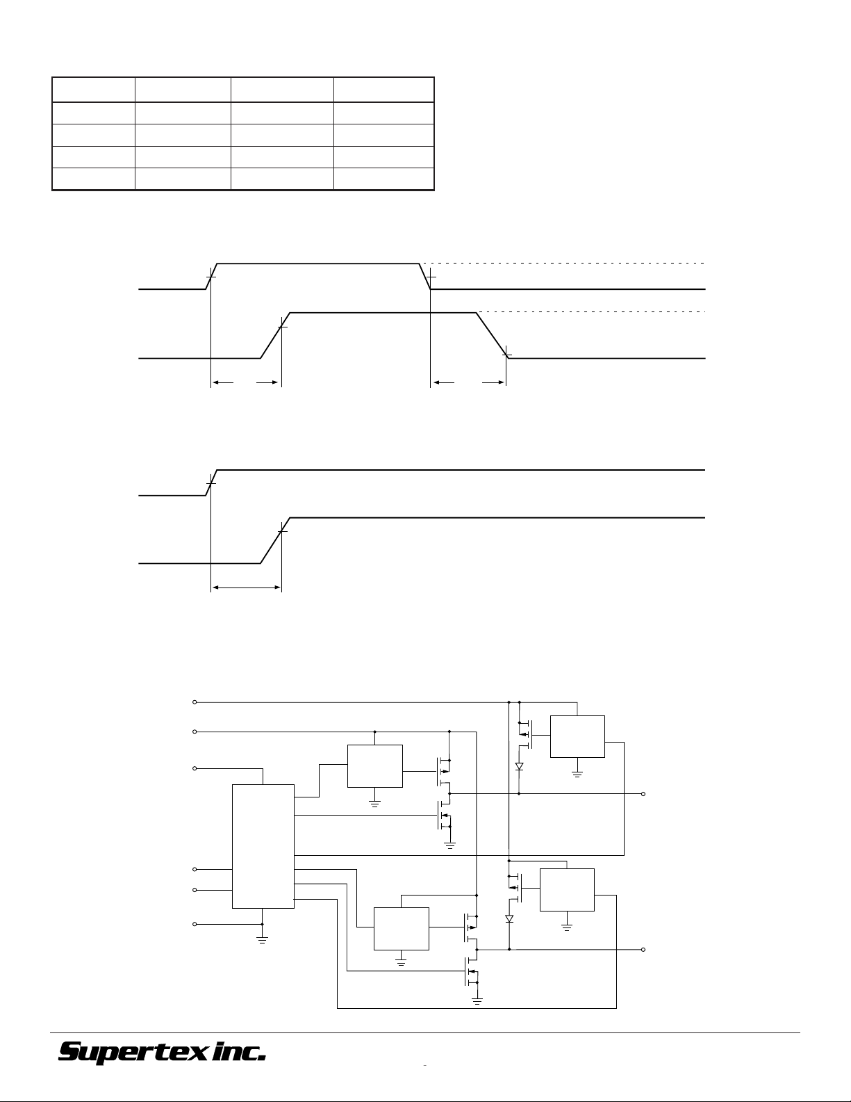
Truth Table
HV
EN
HHHVINGND
HLGND HV
LHLVINGND
LLGND LV
POL HV
OUT1
Timing Diagram
HV
POL
OUT1
GND
50%
t
(ON)
80%
HV
OUT2
IN
IN
Figure 1
50%
t
(OFF)
5%
V
IH
V
IL
VIN
or LV
HV508
IN
HV
EN
HV
OUT1
LV
IN
Block Diagram
LV
IN
HV
IN
V
DD
HV
EN
POL
50%
t
EN
CMOS
(ON)
Logic
80%
Figure 2
Level
Translator
Level
Translator
Level
Translator
HV
OUT
V
IH
V
IL
HV
IN
1
GND
©2001 Supertex Inc. All rights reserved. Unauthorized use or reproduction prohibited.
Level
Translator
HV
2
OUT
12/13/010
1235 Bordeaux Drive, Sunnyvale, CA 94089
3
TEL: (408) 744-0100 • FAX: (408) 222-4895
www.supertex.com
 Loading...