

Page 1

X9DRFF-i+
X9DRFF-iT+
X9DRFF-7+
X9DRFF-7T+
USER’S MANUAL
Revision 1.1
Page 2

The information in this User’s Manual has been carefully reviewed and is believed to be accurate.
The vendor assumes no responsibility for any inaccuracies that may be contained in this document,
and makes no commitment to update or to keep current the information in this manual, or to notify
any person or organization of the updates. Please Note: For the most up-to-date version of this
manual, please see our Website at www.supermicro.com.
Super Micro Computer, Inc. ("Supermicro") reserves the right to make changes to the product
described in this manual at any time and without notice. This product, including software and documentation, is the property of Supermicro and/or its licensors, and is supplied only under a license.
Any use or reproduction of this product is not allowed, except as expressly permitted by the terms
of said license.
IN NO EVENT WILL SUPER MICRO COMPUTER, INC. BE LIABLE FOR DIRECT, INDIRECT,
SPECIAL, INCIDENTAL, SPECULATIVE OR CONSEQUENTIAL DAMAGES ARISING FROM THE
USE OR INABILITY TO USE THIS PRODUCT OR DOCUMENTATION, EVEN IF ADVISED OF
THE POSSIBILITY OF SUCH DAMAGES. IN PARTICULAR, SUPER MICRO COMPUTER, INC.
SHALL NOT HAVE LIABILITY FOR ANY HARDWARE, SOFTWARE, OR DATA STORED OR USED
WITH THE PRODUCT, INCLUDING THE COSTS OF REPAIRING, REPLACING, INTEGRATING,
INSTALLING OR RECOVERING SUCH HARDWARE, SOFTWARE, OR DATA.
Any disputes arising between the manufacturer and the customer shall be governed by the laws of
Santa Clara County in the State of California, USA. The State of California, County of Santa Clara
shall be the exclusive venue for the resolution of any such disputes. Supermicro's total liability for
all claims will not exceed the price paid for the hardware product.
FCC Statement: This equipment has been tested and found to comply with the limits for a Class
A digital device pursuant to Part 15 of the FCC Rules. These limits are designed to provide
reasonable protection against harmful interference when the equipment is operated in a commercial
environment. This equipment generates, uses, and can radiate radio frequency energy and, if not
installed and used in accordance with the manufacturer’s instruction manual, may cause harmful
interference with radio communications. Operation of this equipment in a residential area is likely
to cause harmful interference, in which case you will be required to correct the interference at your
own expense.
California Best Management Practices Regulations for Perchlorate Materials: This Perchlorate
warning applies only to products containing CR (Manganese Dioxide) Lithium coin cells. “Perchlorate
Material-special handling may apply. See www.dtsc.ca.gov/hazardouswaste/perchlorate”.
WARNING: Handling of lead solder materials used in this
product may expose you to lead, a chemical known to
the State of California to cause birth defects and other
reproductive harm.
Manual Revision 1.1
Release Date: November 12, 2013
Unless you request and receive written permission from Super Micro Computer, Inc., you may not
copy any part of this document.
Information in this document is subject to change without notice. Other products and companies
referred to herein are trademarks or registered trademarks of their respective companies or mark
holders.
Copyright © 2013 by Super Micro Computer, Inc.
All rights reserved.
Printed in the United States of America
Page 3

Preface
This manual is written for system integrators, PC technicians and
knowledgeable PC users. It provides information for the installation and use of the
X9DRFF-i+/iT+/7+/7T+ motherboard.
About This Motherboard
The Super X9DRFF-i+/iT+/7+/7T+ motherboard supports dual Intel E5-2600(v2)
Series Processors (Socket R LGA 2011) that offer QPI (Intel QuickPath Interface)
Technology (V.1.1), providing point-to-point connection with a transfer speed of up
to 8.0 TG/s. With the C602 chipset built in, the X9DRFF-i+/iT+/7+/7T+ motherboard
supports Intel® Intelligent Power Node Manager (NM), Management Engine (ME)
Technology, Digital Media Interface (DMI), PCI-E Gen. 3.0 and up to 1866 MHz
DDR3 memory. This motherboard was designed for SMC FatTwin server platforms.
Please refer to our website (http://www.supermicro.com) for CPU and memory
support updates.
Manual Organization
Chapter 1 describes the features, specications and performance of the mother-
board. It also provides detailed information about the Intel C602 chipset.
Chapter 2 provides hardware installation instructions. Read this chapter when in-
stalling the processor, memory modules and other hardware components into the
system. If you encounter any problems, see Chapter 3, which describes trouble-
shooting procedures for video, memory, and system setup stored in the CMOS.
Chapter 4 includes an introduction to the BIOS, and provides detailed instructions
on how to run the CMOS setup utility.
Appendix A provides BIOS error beep codes.
Appendix B lists software installation instructions.
Preface
iii
Page 4

X9DRFF-i+/iT+/7+/7T+ Motherboard User’s Manual
Conventions Used in the Manual
Pay special attention to the following symbols for proper system installation and to
prevent damage to the system or injury to yourself:
Warning: Important information given to ensure proper system installation or to prevent
damage to the components or injury to yourself.
Note: Additional information given to differentiate between various models
or provides information for correct system setup.
iv
Page 5

Contacting Supermicro
Headquarters
Address: Super Micro Computer, Inc.
980 Rock Ave.
San Jose, CA 95131 U.S.A.
Tel: +1 (408) 503-8000
Fax: +1 (408) 503-8008
Email: [email protected] (General Information)
[email protected] (Technical Support)
Web Site: www.supermicro.com
Europe
Address: Super Micro Computer B.V.
Het Sterrenbeeld 28, 5215 ML
's-Hertogenbosch, The Netherlands
Tel: +31 (0) 73-6400390
Fax: +31 (0) 73-6416525
Email: [email protected] (General Information)
[email protected] (Technical Support)
[email protected] (Customer Support)
Preface
Asia-Pacic
Address: Super Micro Computer, Inc.
3F, No. 150, Jian 1st Rd.
Zhonghe Dist., New Taipei City 23511
Taiwan (R.O.C)
Tel: +886-(2) 8226-3990
Fax: +886-(2) 8226-3992
Web Site: www.supermicro.com.tw
Technical Support:
Email: [email protected]
Tel: +886-(2)-8226-3990
v
Page 6

X9DRFF-i+/iT+/7+/7T+ Motherboard User’s Manual
Table of Contents
Preface
Chapter 1 Overview
1-1 Overview ......................................................................................................... 1-1
1-2 Processor and Chipset Overview...................................................................1-11
1-3 Special Features ........................................................................................... 1-12
1-4 PC Health Monitoring .................................................................................... 1-12
1-5 ACPI Features ............................................................................................... 1-13
1-6 Power Supply ................................................................................................ 1-13
1-7 Super I/O ....................................................................................................... 1-13
1-8 Advanced Power Management ..................................................................... 1-14
Intel® Intelligent Power Node Manager (IPNM) ............................................ 1-14
Management Engine (ME) ............................................................................ 1-14
1-9 Overview of the Nuvoton WPCM450 Controller .......................................... 1-14
WPCM450R DDR2 Memory Interface .......................................................... 1-15
WPCM450R PCI System Interface ............................................................... 1-15
Other Features Supported by the WPCM BMC Controller ........................... 1-15
Chapter 2 Installation
2-1 Standardized Warning Statements ................................................................. 2-1
Battery Handling .............................................................................................. 2-1
Product Disposal ............................................................................................. 2-3
2-2 Static-Sensitive Devices .................................................................................. 2-4
Precautions ..................................................................................................... 2-4
Unpacking ....................................................................................................... 2-4
2-3 Processor and Heatsink Installation................................................................ 2-5
Installing the LGA2011 Processor .................................................................2-5
Installing a Passive CPU Heatsink ................................................................. 2-9
Removing the Heatsink ................................................................................. 2-10
2-4 Installing and Removing the Memory Modules ..............................................2-11
Installing & Removing DIMMs ........................................................................2-11
Removing Memory Modules ..........................................................................2-11
2-5 Motherboard Installation ................................................................................ 2-16
Tools Needed ................................................................................................ 2-16
Location of Mounting Holes .......................................................................... 2-16
Installing the Motherboard ............................................................................ 2-17
2-6 Control Panel Connectors and I/O Ports ...................................................... 2-18
Back Panel Connectors and I/O Ports .......................................................... 2-18
vi
Page 7

Table of Contents
Back Panel I/O Port Locations and Denitions ........................................... 2-18
Universal Serial Bus (USB) ...................................................................... 2-19
Video Connection ..................................................................................... 2-19
Ethernet Ports .......................................................................................... 2-20
Serial Port ................................................................................................. 2-20
Power Switch ............................................................................................ 2-21
2-7 Connecting Cables ........................................................................................ 2-22
Fan Headers ............................................................................................. 2-23
TPM Header/Port 80 ................................................................................ 2-23
SATA DOM Power Connector .................................................................. 2-24
Chassis Intrusion ..................................................................................... 2-24
T-SGPIO 1/2 & 6-SGPIO 1/2 Headers ..................................................... 2-25
Power SMB (I2C) Connector .................................................................... 2-25
NMI Header .............................................................................................. 2-26
Unit Identier Switch ................................................................................ 2-27
Battery Backup Unit (BBU) Connector (X9DRF-7+/7T+ Only) ................ 2-28
TFM Module Connector (X9DRF-7+/7T+ Only) ....................................... 2-28
2-8 Jumper Settings ............................................................................................ 2-29
Explanation of Jumpers ................................................................................ 2-29
GLAN Enable/Disable .............................................................................. 2-29
CMOS Clear ............................................................................................. 2-30
Watch Dog Enable/Disable ...................................................................... 2-30
VGA Enable .............................................................................................. 2-31
BMC Enable ............................................................................................ 2-31
Management Engine (ME) Recovery ...................................................... 2-32
Manufacture Mode Select ........................................................................ 2-32
System Reset .......................................................................................... 2-33
SAS Enable (For X9DRFF-7+/7T+) ......................................................... 2-33
2-9 Onboard LED Indicators ............................................................................... 2-35
GLAN LEDs .............................................................................................. 2-35
IPMI Dedicated LAN LEDs ....................................................................... 2-35
HDD Activity LED ..................................................................................... 2-36
BMC Heartbeat LED ................................................................................ 2-36
SAS Heartbeat LED ................................................................................. 2-37
BMC Failure LED ..................................................................................... 2-37
UID LED ................................................................................................... 2-38
SAS Error LEDs ....................................................................................... 2-38
vii
Page 8

X9DRFF-i+/iT+/7+/7T+ Motherboard User’s Manual
2-10 SATA/SAS Connections ................................................................................ 2-39
SATA/SAS Ports ....................................................................................... 2-39
Chapter 3 Troubleshooting
3-1 Troubleshooting Procedures ........................................................................... 3-1
3-2 Technical Support Procedures ........................................................................ 3-4
3-3 Battery Removal and Installation .................................................................... 3-5
3-4 Frequently Asked Questions ........................................................................... 3-6
3-5 Returning Merchandise for Service................................................................. 3-7
Chapter 4 BIOS
4-1 Introduction ...................................................................................................... 4-1
4-2 Main Setup ...................................................................................................... 4-2
4-3 Advanced Setup Congurations...................................................................... 4-4
4-4 Event Logs .................................................................................................... 4-24
4-5 IPMI ............................................................................................................... 4-26
4-6 Boot ............................................................................................................... 4-28
4-7 Security ......................................................................................................... 4-29
4-8 Save & Exit ................................................................................................... 4-30
Appendix A BIOS Error Beep Codes
Appendix B Software Installation Instructions
B-1 Installing Software Programs ..........................................................................B-1
B-2 Conguring SuperDoctor® III (For Window OS Only) .................................... B-2
viii
Page 9

Chapter 1: Overview
Chapter 1
Overview
1-1 Overview
Checklist
Congratulations on purchasing your computer motherboard from an acknowledged
leader in the industry. Supermicro boards are designed with the utmost attention to
detail to provide you with the highest standards in quality and performance.
This motherboard was designed to be used in an SMC-proprietary system as a part
of an integrated system platform.
Note: For your system to work properly, please follow the links below to
download all necessary drivers/utilities and the user's manual for your
motherboard.
SMCI product manuals: http://www.supermicro.com/support/manuals/
Product Drivers and utilities: ftp://ftp.supermicro.com/
If you have any questions, please contact our support team at support@supermicro.
com.
1-1
Page 10
X9DRFF-i+/iT+/7+/7T+ Motherboard User’s Manual
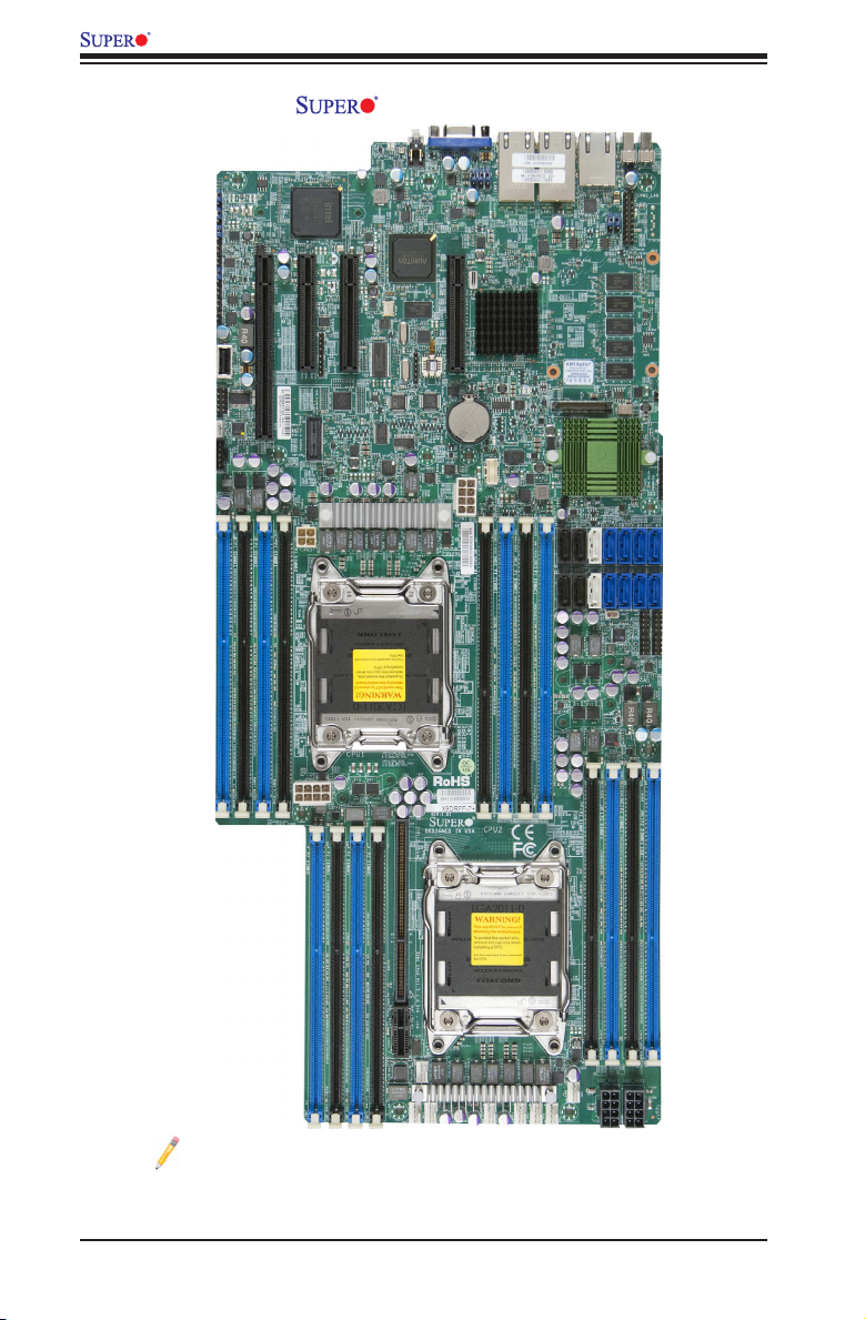
Motherboard Image
Note: All graphics shown in this manual were based upon the latest PCB
Revision available at the time of publishing of the manual. The motherboard
you've received may or may not look exactly the same as the graphics
shown in this manual.
1-2
Page 11
COM1
HDD_PWR1
HDD_PWR2
JPW3
SXB1_1
JPW2
JPW1
FAN7
FAN6
FAN8
FAN5
FAN4
FAN3
FAN2
FAN1
UID_SW1
JPI2C1
PWR_SW1
SXB1_2
FAILURE_LED1
UID_LED1
HDD_FAULT
_LED1
USB0
T-SGPIO2
T-SGPIO1
6-SGPIO1
6-SGPIO2
JSD1
JPL1
JPME1
JPME2
JWD1
JPG1
JP7
JPB1
JP6
JPS1
Rev.1.02
X9DRFF-i(T)+_7(T)+
CPLD1
JPP1
LSI_UART2
LSI_UART1
JBT1
BMC_HB_LED1
HDD_ACT
_LED1
JL1
JNMI1
JRST1
JI2C2
JI2C1
JBAT1
JTPM1
FAN9
#4
#6
#0
#5
#3
#1
CPU2 SLOT4 PCI-E 3.0 X8
CPU1 SLOT3 PCI-E 3.0 X8
PCH SLOT2 PCI-E 2.0 X4 (IN X8)
CPU1 SLOT1 PCI-E 3.0 X16
USB2
VGA
LAN2
LAN1
IPMI_LAN
P1 DIMMA1
P1 DIMMA2
P1 DIMMB1
P1 DIMMB2
P2 DIMMG1
P2 DIMMG2
P2 DIMMH1
CPU1
P2 DIMMH2
P1 DIMMD2
P1 DIMMD1
SXB1 CPU2 PCI-E 3.0 X16 + x16
P1 DIMMC2
P1 DIMMC1
P2 DIMMF2
P2 DIMMF1
P2 DIMME2
P2 DIMME1
#2
BIOS
JPP2
CPU2
CLOSE 1st
OPEN 1st
CLOSE 1st
OPEN 1st
LSI 2208
SAS CTRL
Intel PCH
Intel
LAN CTRL
Nuvotun
BMC
(SAS #0-7)
(SATA #0-5)
SAS_ERR_LED1
SAS_ERR_LED2
SAS_HB_LED1
USB1
JITP1
XDP-CPU
BBU1
#3#1#7
#5
#0
#4
#2
TFM1
Chapter 1: Overview
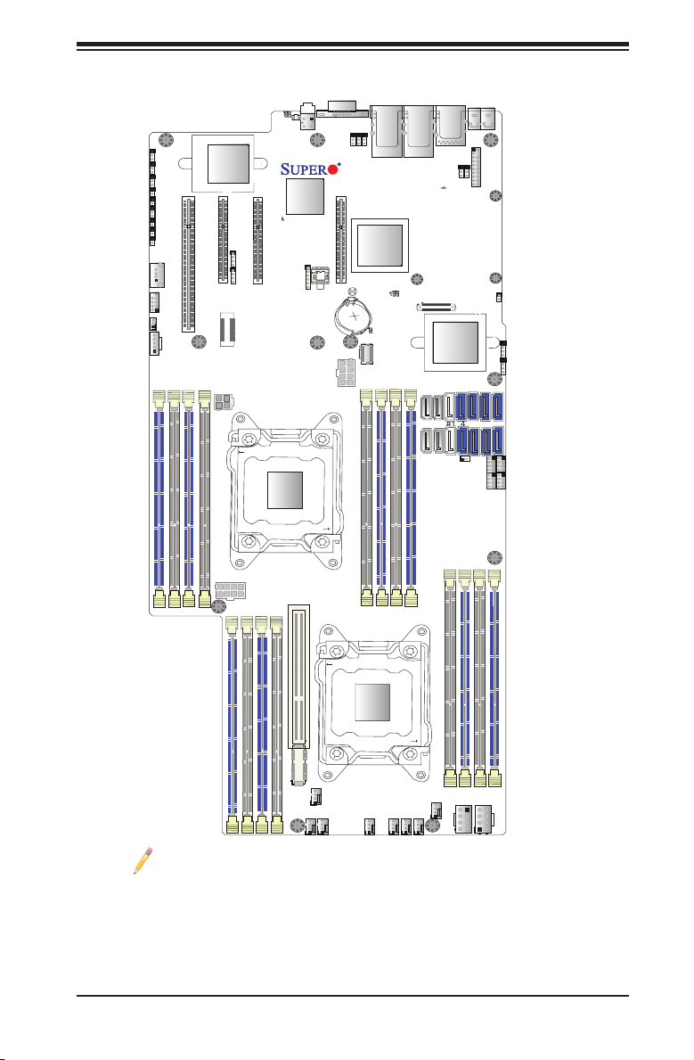
Motherboard Layout
Note 1: For the latest CPU/Memory updates, please refer to our website
at http://www.supermicro.com/products/motherboard/ for details.
Note 2: Changing BMC log-in information is recommended during initial
system power-on. The default username is ADMIN and password is
ADMIN. For BMC best practices, please refer to: http://www.supermicro.
com/products/nfo/les/IPMI/Best_Practices_BMC_Security.pdf
1-3
Page 12
X9DRFF-i+/iT+/7+/7T+ Motherboard User’s Manual
LSI_UART1
LAN2
LAN1
P2 DIMME1
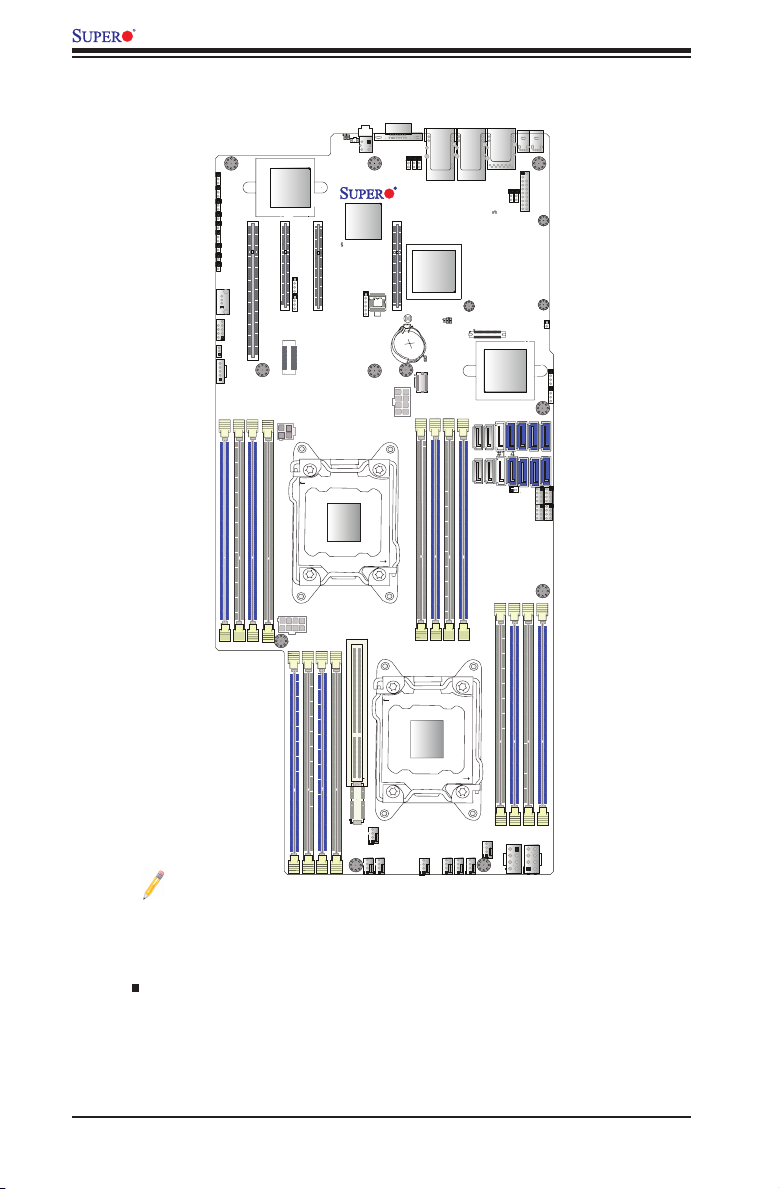
X9DRFF-i+/iT+/7+/7T+ Quick Reference
FAILURE_LED1
UID_LED1
UID_SW1
VGA
PWR_SW1
JPB1
JP6
JPL1
JPME1
JPME2
JNMI1
JWD1
JRST1
JI2C2
JI2C1
JL1
COM1
FAN9
JPI2C1
P1 DIMMA1
USB2
Nuvotun
CPU2 SLOT4 PCI-E 3.0 X8
BMC
CPLD1
BIOS
JBAT1
JPW1
JP7
X9DRFF-i(T)+_7(T)+
Rev.1.02
Intel PCH
JBT1
BBU1
Intel
LAN CTRL
PCH SLOT2 PCI-E 2.0 X4 (IN X8)
JITP1
P1 DIMMB2
JPW3
CPU1 SLOT3 PCI-E 3.0 X8
BMC_HB_LED1
JPP1
JPP2
XDP-CPU
CPU1
CLOSE 1st
CPU1 SLOT1 PCI-E 3.0 X16
P1 DIMMA2
P1 DIMMB1
SAS_ERR_LED2
SAS_HB_LED1
HDD_FAULT
_LED1
IPMI_LAN
_LED1
SAS_ERR_LED1
TFM1
LSI 2208
SAS CTRL
(SAS #0-7)
#4
#2
#3
#5
(SATA #0-5)
USB0
USB1
HDD_ACT
JPG1
JPS1
JTPM1
LSI_UART2
#3#1#7
#0
#5
#2
#6
#1
#0
#4
6-SGPIO2
6-SGPIO1
JSD1
T-SGPIO2
T-SGPIO1
P2 DIMMG1
JPW2
OPEN 1st
P1 DIMMC2
P1 DIMMC1
P1 DIMMD2
P1 DIMMD1
SXB1_2
P2 DIMMH2
P2 DIMMH1
P2 DIMMG2
SXB1 CPU2 PCI-E 3.0 X16 + x16
CPU2
CLOSE 1st
OPEN 1st
SXB1_1
FAN8
FAN4
FAN6
FAN5
FAN7
P2 DIMMF1
P2 DIMME2
P2 DIMMF2
FAN1
HDD_PWR2
FAN3
FAN2
HDD_PWR1
Notes:
•See Chapter 2 for detailed information on jumpers, I/O ports and JF1 front
panel connections.
•" " indicates the location of "Pin 1".
•Jumpers/LED Indicators not indicated are for testing only.
•Use only the correct type of onboard CMOS battery as specied by the manufac-
turer. Do not install the onboard battery upside down to avoid possible explosion.
1-4
Page 13

Chapter 1: Overview
X9DRFF-i+/iT+/7+/7T+ Jumpers
Jumper
JBT1 Clear CMOS See Chapter 2
JI2C1/JI2C2 SMB to PCI-E Slots Open (Disabled)
JPB1 BMC Enable Pins 1-2 (Enabled)
JPG1 VGA Enable Pins 1-2 (Enabled)
JPL1 LAN1/LAN2 Enable Pins 1-2 (Enabled)
JPME1 Management Engine (ME)
JPME2 Management Engine (ME)
JRST1 System Reset Enable Pins 2-3 (Normal)
JPS1 (X9DRFF-7+/7T+ Only) SAS Enable Pins 1-2 (Enabled)
JWD1 Watch Dog Timer Enable Pins 1-2 (Reset)
X9DRFF-i+/iT+/7+/7T+ Connectors
Connectors Description
BBU1 SAS Battery Backup Unit (BBU)
COM1 Serial (COM) Port
FAN1-FAN8,
FAN9 (Rear_FAN1)
HDD_PWR1/HDD_PWR2 8-pin Power Supply Connectors for HDD Device Use
JBAT1 Onboard CMOS Battery (See Chpt. 3 for Battery Dis-
JL1 Chassis Intrusion Header
JNMI1 Non-maskable Interrupt Header
JPI2C1 Power Supply SMBbus I2C Header
JPW1/JPW2 8-pin Power Connectors
JPW3 4-pin Power Connector (PS_ON_N)
JSD1 SATA DOM (Device on Module) Power Connector
JTPM1 TPM (Trusted Platform Module)/Port 80
LAN1/LAN2 G-bit Ethernet LAN Ports 1/2 (X9DRFF-i+/7+),
(IPMI) LAN IPMI LAN
PWR_SW1 Power Switch
(I-)SATA 0/1 SATA 3.0 Connectors 0/1 from Intel AHCI
(I-) SATA 2-5 SATA 2.0 Connectors 2/3/4/5 from Intel AHCI
(L)-SAS 0-7
(X9DRFF-7+/7T+ Only)
Description Default Setting
Pins 1-2 (Normal)
Recovery Mode
Pins 1-2 (Normal)
Manufacture Mode
CPU/System/Cooling Fan Headers
posal)
10 G_bit (TLAN) LAN Ports 1/2 (X9DRFF-iT+/7T+)
SAS 2.0 Connections 0-7 supported by the LSI 2208
SAS Controller
1-5
Page 14

X9DRFF-i+/iT+/7+/7T+ Motherboard User’s Manual
6-SGPIO 1
(X9DRFF-7+/7T+)
T-SGPIO 1/2 Serial_Link General Purpose I/O Headers 1/2 for Intel
(CPU1) Slot1 PCI-Exp. 3.0 x16 Slot
(CPU1) Slot3/(CPU2)Slot4 PCI-Exp. 3.0 x8 Slots
(PCH) Slot2 PCI-Exp. 3.0 x4 in x8 Slot
SXB1 (CPU2) PCI-E 3.0
x16 + 16 Slot
TFM1 (X9DRFF-7+/7T+
Only)
UID_SWI UID (Unit Identifer) Switch (SW1)
USB0/USB1 Backplane USB 0/ USB1 Ports
USB2 Front Accessible USB 2 Port
VGA (Backplane) VGA Port
X9DRFF-i+/iT+/7+/7T+ LED Indicators
LED Description State Status
BMC_HB_LED1 BMC Heartbeat LED Green: Blinking BMC Normal
HDD_ACT_LED1 HDD Activity LED Green: Blinking HDD Active
HDD_Fault_LED1 HDD Error LED Red: On
Serial_Link General Purpose I/O Header for L-SATA
0-5 Connectors
SATA Connections
PCI-Exp. 3.0 x16 + 16 SMC-Proprietary Slot (SXB1)
TFM Module Connector for Super Cap (Capacitor)
support (Super Cap Battery Pack Kit: Part# BTR0024LH-LSI00297)
Error(s) in HDD
Connections
Failure_LED1 BMC Failure Red: On BMC Failure
SAS_HB_LED1 SAS Heartbeat LED Green: Blinking SAS Normal
SAS_Fault_LED1
(For X9DRFF7+/7T+)
SAS_Fault_LED2
(For X9DRFF7+/7T+)
UID_LED1 UID LED Blue: On Unit Identied
Warning: To avoid damaging your motherboard and components, please use a
power supply that supports a 24-pin, two 8-pin and one 4-pin power connectors. Be
sure to connect the 24-pin and the 8-pin power connectors to your power supply
for adequate power delivery to your system. The 4-pin power connector is optional;
however, Supermicro recommends that this connector also be plugged in for optimal
power delivery.
SAS Error LED 1 Red: On
SAS Error LED 2 Red: On
Error(s) in SAS
Connections
Error(s) in SAS
Connections
1-6
Page 15

Motherboard Features
Chapter 1: Overview
CPU
Memory
Chipset
Expansion
Slot
Graphics
Network
• Dual Intel
LGA 2011); each processor supports four full-width
Intel QuickPath Interconnect (QPI) links (with support
of up to 25.6 GT/s per QPI link and with Data Transfer
Rate of up to 8.0 GT/s per direction).
®
E5-2600(v2) Series Processors (Socket R
Note: For Intel E5-2600(v2) processor support,
BIOS version 3.0 or above is required.
•Integrated memory controller supports up to 1 TB
of Load Reduced (LRDIMM), 512 GB of Registered
(RDIMM) or 128 GB of Unbuffered (UDIMM) ECC/
Non-ECC DDR3 800/1066/1333/1600/1866 MHz
240-pin 4-channel memory modules in 16 DIMM
slots.
Note 1: 1866 MHz memory speed is dependent
on Intel E5-2600v2 CPUs.
Note 2: For the latest memory updates, please
refer to the Tested Memory List posted on our
website (http://www.supermicro.com/products/
motherboard).
• Intel® C602 Chipset
• One (1) PCI-E 3.0 x32 (SMC-Proprietary) slot (CPU2
3.0 x16 + X16 Slot SXB1)
• One (1) PCI-E 3.0 x16 slot (CPU1 Slot 1)
• One (1) PCI-E 3.0 x4 in x8 slot (PCH Slot 2)
• Two (2) PCI-E 3.0 x8 slots (CPU1 Slot 3/CPU2 Slot 4)
• Nuvoton WPCM450R G200 Graphics Controller
• Intel X540 dual-channel 10G Base-T (T) Ethernet
controller for LAN 1/LAN 2 ports (X9DRFF-iT+/7T+
only),
• Intel i350 dual-channel Gigabit (10/100/1000 Mb/s)
Ethernet controller for LAN 1/LAN 2 ports (for
X9DRFF-i+/7+)
• Nuvoton WPCM450R Base-Board Controller (BMC)
supports IPMI_LAN 2.0
1-7
Page 16

X9DRFF-i+/iT+/7+/7T+ Motherboard User’s Manual
I/O Devices
Peripheral
Devices
BIOS
Power
Cong.
PC Health
Monitoring
SATA Connections
• SATA Ports Two (2) SATA 3.0 (I-SATA 0/1),
Four (4) SATA 2.0 Ports from
Intel AHCI (I-SATA 2-5),
• RAID RAID 0, 1, 5, 10 (Windows
OS and Latest Linux Latest
Kernel)
SAS Ports (X9DRFF-7+/7T+ Only)
• SAS Ports Eight (8) SAS 2.0 Ports from
LSI 2208 SAS Controller
• RAID RAID 0, 1, 5, 6, 10, 50, 60 (via
LSI 2208)
Integrated IPMI 2.0
• IPMI 2.0 supported by the WPCM450R BMC
Serial (COM) Port
• One (1) Fast UART 16550 Connection: 9-pin RS-
232 port
Super I/O
• Winbond Super I/O 83527HG
USB Devices
• Two (2) USB ports on the rear I/O panel (USB 0/1),
• One (1) USB port for front panel access (JUSB 2)
• 16 MB SPI AMI BIOS
®
SM Flash BIOS
• APM 1.2, DMI 2.3, PCI 2.3, ACPI 1.0/2.0/3.0/4.0,
USB Keyboard, Plug & Play (PnP) and SMBIOS 2.5
• ACPI/ACPM Power Management
• Main switch override mechanism
• Intel® Intelligent Power Node Manager (NM)
• Management Engine (ME)
Note: Special power supply required. See the
note on IPNM support on Page 1-14.
• Keyboard Wake-up from Soft-Off
• Power-on mode for AC power recovery
CPU Monitoring
• Onboard voltage monitors for 3.3V, +3.3VSB, 5V,
+5VSB, +12V/-12V, VBAT, HT, memory voltages,
CPU core voltages, chipset voltages.
1-8
Page 17

Chapter 1: Overview
• CPU 5 Phase switching voltage regulator
• CPU/System overheat LED and control
• CPU Thermal Design Power (TDP): supports up to
130W (See Note 1 next page)
• CPU Thermal Trip support
• Thermal Monitor 2 (TM2) support
Fan Control
• Fan status monitoring with rmware 4-pin (Pulse
Width Modulation) fan speed control
• Low noise fan speed control
System
Management
• PECI (Platform Environment Conguration Interface)
2.0 support
• System resource alert via SuperDoctor® III
• SuperDoctor® III, Watch Dog, NMI
• Chassis Intrusion Header and Detection
Dimensions
Note 1: CPU Maximum Thermal Design Power (TDP) is subject to chassis
and heatsink cooling restrictions. For proper thermal management, please
check the chassis and heatsink specications for proper CPU TDP sizing.
• 18.72" (L) x 8.54" (W) (475.49 mm x 216.92 mm)
Note 2: For IPMI Conguration Instructions, please refer to the Embedded
IPMI Conguration User's Guide available @ http://www.supermicro.com/
support/manuals/.
Note 3: Changing BMC log-in information is recommended during initial
system power-on. The default username is ADMIN and password is
ADMIN. For BMC best practices, please refer to: http://www.supermicro.
com/products/nfo/les/IPMI/Best_Practices_BMC_Security.pdf
1-9
Page 18
X9DRFF-i+/iT+/7+/7T+ Motherboard User’s Manual
Gen3 x16 x16
Gen3 x8
#1
PCI-Ex16x16
RJ45
RJ45
#1
Proprietary SLOT
PCI-Ex8 SLOT
J3
LAN
X540
I350 (2 ports)
J1 J2
J3
PCI-Ex16 SLOT
PCI-E x4 in x8 SLOT
DDR3
DDR3 DIMM
DDR3 DIMM
PCI-E x8 SLOT
DDR3
E
C
DDR3
DDR3
F
DDR3 DIMM
#1#1
D
DDR3 DIMM
Gen3 x8 (0~7)
Gen2 x4
Gen3 x16
Gen3 x8 (8~15)
SAS2208
DDR3
SAS
SAS2 #0
SAS2 #1
SAS2 #2
SAS2 #3
SAS2 #4
SAS2 #5
SAS2 #6
SAS2 #7
PE2PE1 DMI
PE3
CPU1
Rear (Fan Side)
E5-2600(v2) Series Processor
P0 P1
QPI
QPI
P1 P0
CPU0
Front (I/O Side)
E5-2600(v2) Series Processor
PE3
PE2PE1 DMI
Gen3 x8 (0~7)
BBU Conn
TFM
Super-CAP
H
B
AT25321
SPI
DMI
PCH C602
PEG0
PEG1_4:1
PEG1_8
WPCM450
VGA BMC
DDR2
VGA CONN
G
DDR3 DIMM
#1
A
DDR3 DIMM
SATA
PHY
RTL8201F
LAN
AHCI
#1#1
DDR3 DIMM
#1
DDR3 DIMM
SCU
USB
LPCPCI-32bit
3/1.5
3/1.5
3/1.5
3/1.5
6/3/1.5
6/3/1.5
SATA
USB
TPM
SATA2 #5
SATA2 #4
SATA2 #3
SATA2 #2
SATA3 #1
SATA3 #0
DOM on I-SATA
0 1 2
Single
Single
Type A
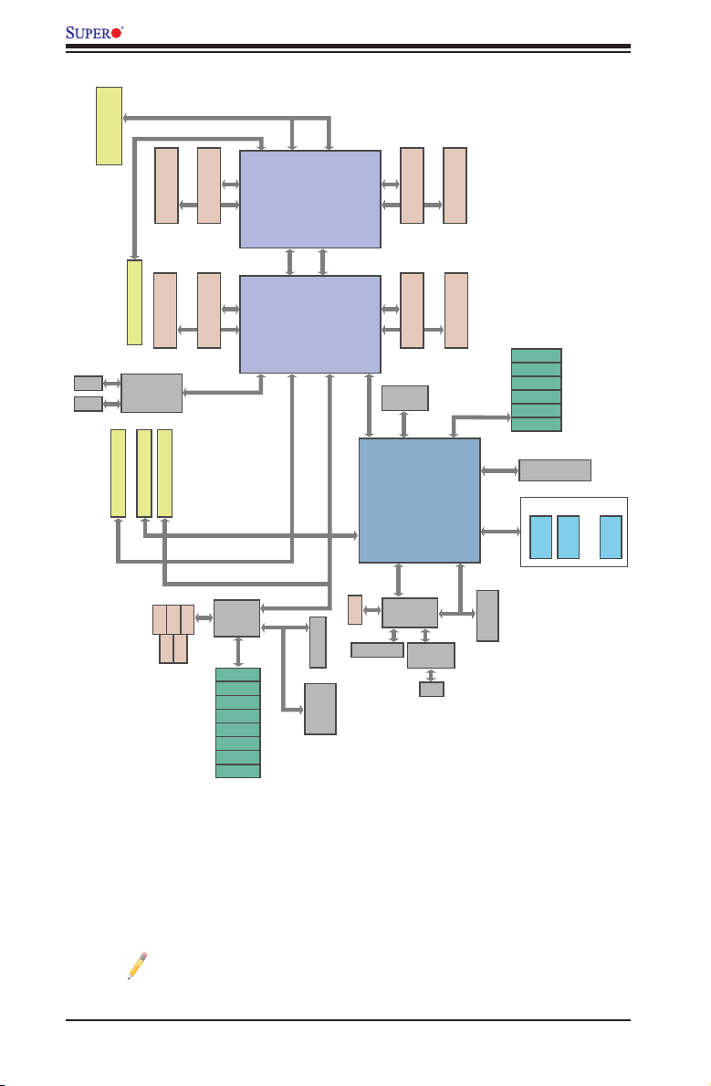
System Block Diagram
Note: This is a general block diagram and may not exactly represent the
features on your motherboard. See the Motherboard Features pages for
the actual specications of each motherboard.
1-10
Page 19

Chapter 1: Overview
1-2 Processor and Chipset Overview
Built upon the functionality and the capability of Intel E5-2600(v2) Series Pro-
cessors (Socket R LGA 2011) and the C602 chipset, the X9DRFF-i+/iT+/7+/7T+
motherboard provides the performance and feature sets required for dual_pro-
cessor-based Fat Twin server platforms. (See note below for processor support.)
With support of Intel QuickPath interconnect (QPI) Technology, the X9DRFF-i+/
iT+/7+/7T+ offers point-to-point serial interconnect interface with a transfer speed
of up to 8.0 GT/s, providing superb system performance.
The C602 chipset provides extensive IO support, including the following functions
and capabilities:
•PCI-E 2.0 and 3.0 support
•ACPI Power Management Logic Support, Rev. 3.0b
•Intel® Intelligent Power Node Management (NM) (Special power supply cables
required)
•Management Engine (ME)
•Intel Rapid Storage Technology supported
•Intel Virtualization Technology for Directed I/O (Intel VT-d) supported
•Intel Trusted Execution Technology supported
•Serial Peripheral Interface (SPI) Supported
•Intel Anti-Theft Technology (Intel AT) supported
•Digital Media Interface (DMI) supported
•Advanced Host Controller Interface (AHCI) supported
•Compatibility Modules (DMA Controller, Timer/Counters, Interrupt Controller)
supported
Note: For Intel E5-2600(v2) processor support, BIOS version 3.0 or above
is required.
1-11
Page 20

X9DRFF-i+/iT+/7+/7T+ Motherboard User’s Manual
1-3 Special Features
Recovery from AC Power Loss
The Basic I/O System (BIOS) provides a setting that determines how the system will
respond when AC power is lost and then restored to the system. You can choose for
the system to remain powered off (in which case you must press the power switch
to turn it back on), or for it to automatically return to the power-on state. See the
Advanced BIOS Setup section for this setting. The default setting is Last State.
1-4 PC Health Monitoring
This section describes the features of PC health monitoring of the motherboard.
This motherboard has an onboard System_Hardware_Monitor chip that supports
PC health monitoring. An onboard voltage monitor will scan the following onboard
voltages continuously: Onboard voltage monitors for 3.3V, +3.3VSB, 5V, +5VSB,
+12V/-12V, VBAT, HT, memory voltages, chipset voltages and CPU core voltages .
Once a voltage becomes unstable, a warning is given, or an error message is sent
to the screen. The user can adjust the voltage thresholds to dene the sensitivity
of the voltage monitor.
Environmental Temperature Control
A thermal control sensor monitors the CPU temperatures in real time and will turn
on the thermal control fans whenever the CPU temperature exceeds a user-dened
threshold. The overheat circuitry runs independently from the CPU. Once it detects
that the CPU temperature is too high, it will automatically turn on the thermal fan
control to prevent the CPU from overheating. The onboard chassis thermal circuitry
can monitor the overall system temperature and alert the user when the chassis
temperature is too high.
Note: To avoid possible system overheating, please be sure to provide
adequate airow to your system.
1-12
Page 21

Chapter 1: Overview
System Resource Alert
This feature is available when used with SuperDoctor® III in the Windows OS
environment or used with SuperDoctor II in Linux. SuperDoctor is used to notify
the user of certain system events. For example, you can congure SuperDoctor
to provide you with warnings when the system temperature, CPU temperatures,
voltages, and fan speeds go beyond a predened range.
1-5 ACPI Features
ACPI stands for Advanced Conguration and Power Interface. The ACPI specica-
tion denes a exible and abstract hardware interface that provides a standard
way to integrate power management features throughout a PC system, including
its hardware, operating system and application software. This enables the system
to automatically turn on and off peripherals such as CD-ROMs, network cards, hard
disk drives and printers.
In addition to operating_system-directed power management, ACPI also provides
a generic system event mechanism for Plug and Play, and an operating system-
independent interface for conguration control. ACPI leverages the Plug and
Play BIOS data structures while providing a processor_architecture-independent
implementation that is compatible with Windows 7, Windows 8, and Windows 2008
Operating Systems.
Slow Blinking LED for Suspend-State Indicator
When the CPU goes into a suspend state, the chassis power LED will start blinking
to indicate that the CPU is in the suspend mode. When the user presses any key,
the CPU will "wake up," and the LED will automatically stop blinking and remain on.
1-6 Power Supply
As with all computer products, a stable power source is necessary for proper and
reliable operation. It is even more important for processors that have high CPU
clock rates.
The X9DRFF-i+/iT+/7+/7T+ motherboard was designed to be installed in Supermicro
-Proprietary Fat Twin chassis as a integrated platform solution. Please refer to your
server manual for power supply requirement.
1-7 Super I/O
The Super I/O provides functions that comply with ACPI (Advanced Conguration
and Power Interface), which includes support of legacy and ACPI power manage-
1-13
Page 22

X9DRFF-i+/iT+/7+/7T+ Motherboard User’s Manual
ment through an SMI or SCI function pin. It also features auto power management
to reduce power consumption.
Note 1: For more information on IPMI conguration, please refer to the
IPMI User's Guide posted on our website at http://www.supermicro.com/
support/manuals/.
Note 2: The term "IPMI controller" and the term "BMC controller" can be
used interchangeably in this section.
1-8 Advanced Power Management
The new advanced power management features supported by this motherboard
include IPNM and ME. Please note that you will need to do the following to use
these two new features:
•Use a power supply that supports PMBus 1.1 or 1.2.
•Install the NMView software in your system. NMView is optional and can be
purchased from Supermicro.
Intel® Intelligent Power Node Manager (IPNM)
The Intel® Intelligent Power Node Manager (IPNM) provides your system with
real-time thermal control and power management for maximum energy efciency.
Although IPNM is supported by the BMC (Baseboard Management Controller),
your system must also have IPNM-compatible Management Engine (ME) rmware
installed in your system for IPNM support.
Note: Support for IPNM Specication Version 1.5 or Vision 2.0 depends
on the power supply used in the system.
Management Engine (ME)
The Management Engine, which is an ARC controller embedded in the PCH, pro-
vides Server Platform Services (SPS) to your system. The services provided by
SPS are different from those provided by the ME on client platforms.
1-9 Overview of the Nuvoton WPCM450 Controller
Note: The term "IPMI controller" and the term "BMC controller" can be
used interchangeably in this section.
The Nuvoton WPCM450R Controller, a Baseboard Management Controller (BMC),
supports 2D/VGA-compatible Graphic Cores with PCI interface, creating multi-media
1-14
Page 23

Chapter 1: Overview
virtualization via Keyboard/Video/Mouse Redirection (KVMR). The WPCM450R
Controller is ideal for remote system management.
The WPCM450R Controller interfaces with the host system via PCI connections
to communicate with the graphics cores. It supports USB 2.0 and 1.1 for remote
keyboard/mouse/virtual media emulation. It also provides LPC interface support to
control Super IO functions. The WPCM450R Controller is connected to the network
via an external Ethernet PHY module or shared NCSI connections.
The WPCM450R communicates with onboard components via six SMBus inter-
faces, PECI (Platform Environment Control Interface) buses, and General Purpose
I/O ports.
WPCM450R DDR2 Memory Interface
The WPCM450R supports a 16-bit DDR2 memory module with a speed of up to 220
MHz. For best signal integrity, the WPCM450R provides point-to-point connection.
WPCM450R PCI System Interface
The WPCM450R provides 32-bit, 33 MHz 3.3V PCI interface, which is compliant
with the PCI Local Bus Specication Rev. 2.3. The PCI system interface connects
to the onboard PCI Bridge used by the graphics controller.
Other Features Supported by the WPCM BMC Controller
The WPCM450R supports the following features:
•IPMI 2.0
•Serial over LAN
•KVM over LAN
•LAN Alerting-SNMP Trap
•Event Log
•X-Bus parallel interface for I/O expansion
•Multiple ADC inputs, Analog and Digital Video outputs
•SPI Flash Host BIOS and rmware bootstrap program supported
•Reduced Media Independent Interface (RMII)
1-15
Page 24

X9DRFF-i+/iT+/7+/7T+ Motherboard User’s Manual
•OS (Operating System) Independency
•Provides remote Hardware Health Monitoring via IPMI. Key features
•Provides Network Management Security via remote access/console redirection.
•Supports the following Management tools: IPMIView, CLI (Command Line
Interface)
•RMCP+ protocol supported
Note 1: For more information on IPMI conguration, please refer to the
IPMI User's Guide posted on our website at http://www.supermicro.com/
support/manuals/.
Note 2: The term "IPMI controller" and the term "BMC controller" can be
used interchangeably in this section.
1-16
Page 25

Chapter 2: Installation
Chapter 2
Installation
2-1 Standardized Warning Statements
The following statements are industry-standard warnings, provided to warn the user
of situations which have the potential for bodily injury. Should you have questions or
experience difculty, contact Supermicro's Technical Support department for assis-
tance. Only certied technicians should attempt to install or congure components.
Read this section in its entirety before installing or conguring components in the
Supermicro chassis.
Battery Handling
Warning!
There is a danger of explosion if the battery is replaced incorrectly. Replace the
battery only with the same or equivalent type recommended by the manufacturer.
Dispose of used batteries according to the manufacturer's instructions
電池の取り扱い
電池交換が正しく行われなかった場合、破裂の危険性があります。 交換する電池はメー
カーが推奨する型、または同等のものを使用下さい。 使用済電池は製造元の指示に従
って処分して下さい。
警告
电池更换不当会有爆炸危险。请只使用同类电池或制造商推荐的功能相当的电池更
换原有电池。请按制造商的说明处理废旧电池。
警告
電池更換不當會有爆炸危險。請使用製造商建議之相同或功能相當的電池更換原有
電池。請按照製造商的說明指示處理廢棄舊電池。
Warnung
Bei Einsetzen einer falschen Batterie besteht Explosionsgefahr. Ersetzen Sie die
Batterie nur durch den gleichen oder vom Hersteller empfohlenen Batterietyp.
Entsorgen Sie die benutzten Batterien nach den Anweisungen des Herstellers.
2-1
Page 26

X9DRFF-i+/iT+/7+/7T+ Motherboard User’s Manual
Attention
Danger d'explosion si la pile n'est pas remplacée correctement. Ne la remplacer
que par une pile de type semblable ou équivalent, recommandée par le fabricant.
Jeter les piles usagées conformément aux instructions du fabricant.
¡Advertencia!
Existe peligro de explosión si la batería se reemplaza de manera incorrecta. Re-
emplazar la batería exclusivamente con el mismo tipo o el equivalente recomen-
dado por el fabricante. Desechar las baterías gastadas según las instrucciones
del fabricante.
!הרהזא
תנכס תמייקץוציפ .הניקת אל ךרדב הפלחוהו הדימב הללוסה לש ףילחהל שי
גוסב הללוסה תא מ םאותה תרבחלמומ ןרציתצ.
תוללוסה קוליס תושמושמה עצבל שי .ןרציה תוארוה יפל
경고!
배터리가 올바르게 교체되지 않으면 폭발의 위험이 있습니다. 기존 배터리와 동일
하거나 제조사에서 권장하는 동등한 종류의 배터리로만 교체해야 합니다. 제조사
의 안내에 따라 사용된 배터리를 처리하여 주십시오.
Waarschuwing
Er is ontplofngsgevaar indien de batterij verkeerd vervangen wordt. Vervang de
batterij slechts met hetzelfde of een equivalent type die door de fabrikant aan-
bevolen wordt. Gebruikte batterijen dienen overeenkomstig fabrieksvoorschriften
afgevoerd te worden.
2-2
Page 27

Chapter 2: Installation
Product Disposal
Warning!
Ultimate disposal of this product should be handled according to all national laws
and regulations.
製品の廃棄
この製品を廃棄処分する場合、国の関係する全ての法律・条例に従い処理する必要が
ありま す。
警告
本产品的废弃处理应根据所有国家的法律和规章进行。
警告
本產品的廢棄處理應根據所有國家的法律和規章進行。
Warnung
Die Entsorgung dieses Produkts sollte gemäß allen Bestimmungen und Gesetzen
des Landes erfolgen.
¡Advertencia!
Al deshacerse por completo de este producto debe seguir todas las leyes y regla-
mentos nacionales.
Attention
La mise au rebut ou le recyclage de ce produit sont généralement soumis à des
lois et/ou directives de respect de l'environnement. Renseignez-vous auprès de
l'organisme compétent.
רצומה קוליס
!הרהזא
ו תויחנהל םאתהב תויהל בייח הז רצומ לש יפוס קוליס.הנידמה יקוח
2-3
Page 28

X9DRFF-i+/iT+/7+/7T+ Motherboard User’s Manual
경고!
이 제품은 해당 국가의 관련 법규 및 규정에 따라 폐기되어야 합니다.
Waarschuwing
De uiteindelijke verwijdering van dit product dient te geschieden in overeenstemming
met alle nationale wetten en reglementen.
2-2 Static-Sensitive Devices
Electrostatic Discharge (ESD) can damage electronic com ponents. To avoid dam-
aging your system board, it is important to handle it very carefully. The following
measures are generally sufcient to protect your equipment from ESD.
Precautions
•Use a grounded wrist strap designed to prevent static discharge.
•Touch a grounded metal object before removing the motherboard from the
antistatic bag.
•Handle the board by its edges only; do not touch its components, peripheral
chips, memory modules or gold contacts.
•When handling chips or modules, avoid touching their pins.
•Put the motherboard and peripherals back into their antistatic bags when not
in use.
•For grounding purposes, make sure that your system chassis provides excellent
conductivity between the power supply, the case, the mounting fasteners and
the motherboard.
Unpacking
The motherboard is shipped in antistatic packaging to avoid static damage. When
unpacking the motherboard, make sure that the person handling it is protected
against static.
2-4
Page 29

Chapter 2: Installation
2-3 Processor and Heatsink Installation
Warning: When handling the processor package, avoid placing direct pressure on
the label area.
Notes:
•Always connect the power cord last, and always remove it before adding,
removing or changing any hardware components. Make sure that you install
the processor into the CPU socket before you install the CPU heatsink.
Also, be sure to install a processor in CPU Socket 1 before populating
CPU Socket 2.
•If you buy a CPU separately, make sure that you use an Intel-certied multi-
directional heatsink only.
•Make sure to install the system board into the chassis before you install
the CPU heatsink.
•When receiving a server board without a processor pre-installed, make sure
that the plastic CPU socket cap is in place and none of the socket pins are
bent; otherwise, contact your retailer immediately.
•Refer to the Supermicro website for updates on CPU support.
Installing the LGA2011 Processor
1. There are two load levers on the LGA2011 socket. To open the socket cover,
rst press and release the load lever labeled 'Open 1st'.
1
WARNING!
OPEN 1st
Press down
on
labeled 'Open 1st'.
2
WARNING!
OPEN 1st
Load Lever
2-5
Page 30

X9DRFF-i+/iT+/7+/7T+ Motherboard User’s Manual
2. Press the second load lever labeled 'Close 1st' to release the load plate that
covers the CPU socket from its locking position.
1
Press down on
Load the
Lever labeled 'Close 1st'
WARNING!
OPEN 1st
2
Pull lever away from
the socket
WARNING!
OPEN 1st
Pin 1
3. With the lever labeled 'Close 1st' fully retracted, gently push down on the
'Open 1st' lever to open the load plate. Lift the load plate to open it com-
pletely.
Gently push
down to pop the
1
load plate open.
WARNING!
OPEN 1st
2
WARNING!
2-6
Page 31
Chapter 2: Installation
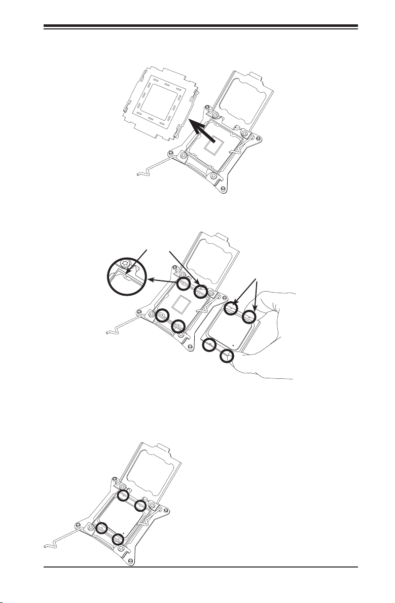
1. Using your thumb and the index nger, remove the 'WARNING' plastic cap
from the socket.
WARNING!
2. Use your thumb and index nger to hold the CPU on its edges. Align the CPU
keys, which are semi-circle cutouts, against the socket keys.
Socket Keys
CPU Keys
3. Once they are aligned, carefully lower the CPU straight down into the socket.
(Do not drop the CPU on the socket. Do not move the CPU horizontally or
vertically. Do not rub the CPU against the surface or against any pins of the
socket to avoid damaging the CPU or the socket.)
Warning: You can only install the CPU
inside the socket in one direction. Make
sure that it is properly inserted into the
CPU socket before closing the load
plate. If it doesn't close properly, do not
force it as it may damage your CPU.
Instead, open the load plate again and
double-check that the CPU is aligned
properly.
2-7
Page 32
X9DRFF-i+/iT+/7+/7T+ Motherboard User’s Manual
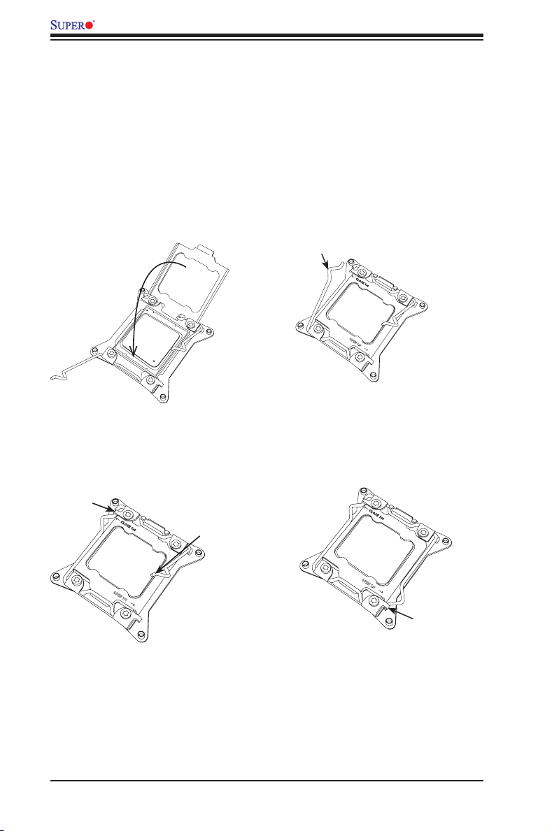
4. With the CPU inside the socket, inspect the four corners of the CPU to make
sure that the CPU is properly installed.
5. Close the load plate with the CPU inside the socket. Lock the lever labeled
'Close 1st' rst, and then lock the lever labeled 'Open 1st' second. Use your
thumb to gently push the load levers down to the lever locks.
1 2
Gently close
the load plate.
Push down and lock the
level labeled 'Close 1st'.
OPEN 1st
3
Lever Lock
4
Push down and
lock the lever
labeled 'Open 1st'
OPEN 1st
OPEN 1st
Lever Lock
2-8
Page 33
Chapter 2: Installation
Installing a Passive CPU Heatsink
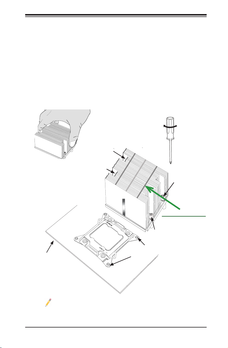
1. Do not apply any thermal grease to the heatsink or the CPU die -- the re-
quired amount has already been applied.
2. Place the heatsink on top of the CPU so that the four mounting holes are
aligned with those on the motherboard's and the heatsink bracket underneath.
3. Screw in two diagonal screws (i.e., the #1 and the #2 screws) until just snug
(-do not over-tighten the screws to avoid possible damage to the CPU.)
4. Finish the installation by fully tightening all four screws.
Screw#1
Screw#3
Screw#4
Motherboard
Notes: 1. For optimized airow, please follow your chassis airow direction
to install the correct CPU heatsink direction. 2. Graphic drawings included
in this manual are for reference only. They might look different from the
components installed in your system.
OPEN 1st
DirectionofAirow
Screw#2
Mounting Holes
2-9
Page 34
X9DRFF-i+/iT+/7+/7T+ Motherboard User’s Manual
Removing the Heatsink
Warning: We do not recommend that the CPU or the heatsink be removed. However,
if you do need to uninstall the heatsink, please follow the instructions below to avoid
damaging the CPU or the CPU socket.
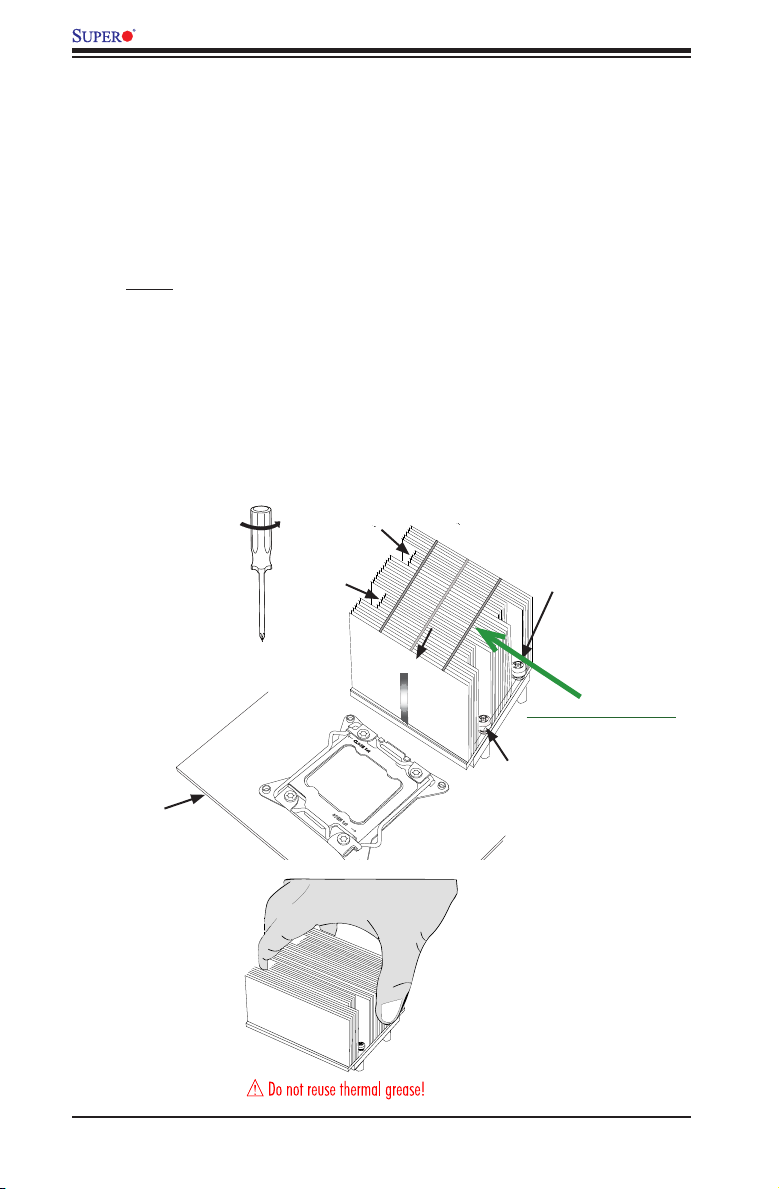
1. Unscrew the heatsink screws from the motherboard in the sequence as
shown in the illustration below.
2. Gently wriggle the heatsink to loosen it from the CPU. (Do not use excessive
force when wriggling the heatsink!)
3. Once the CPU is loosened from the heatsink, remove the CPU from the CPU
socket.
4. Remove the used thermal grease, and clean the surface of the CPU and the
heatsink, Reapply the proper amount of thermal grease on the surface before
reinstalling the CPU and the heatsink.
Loosen screws
in sequence as
shown.
Motherboard
Screw#1
Screw#3
OPEN 1st
Screw#4
DirectionofAirow
Screw#2
2-10
Page 35
Chapter 2: Installation
COM1
HDD_PWR1
HDD_PWR2
JPW3
SXB1_1
JPW2
JPW1
FAN7
FAN6
FAN8
FAN5
FAN4
FAN3
FAN2
FAN1
UID_SW1
JPI2C1
PWR_SW1
SXB1_2
FAILURE_LED1
UID_LED1
HDD_FAULT
_LED1
USB0
T-SGPIO2
T-SGPIO1
6-SGPIO1
6-SGPIO2
JSD1
JPL1
JPME1
JPME2
JWD1
JPG1
JP7
JPB1
JP6
JPS1
Rev.1.02
X9DRFF-i(T)+_7(T)+
CPLD1
JPP1
LSI_UART2
LSI_UART1
JBT1
BMC_HB_LED1
HDD_ACT
_LED1
JL1
JNMI1
JRST1
JI2C2
JI2C1
JBAT1
JTPM1
FAN9
#4
#6
#0
#5
#3
#1
CPU2 SLOT4 PCI-E 3.0 X8
CPU1 SLOT3 PCI-E 3.0 X8
PCH SLOT2 PCI-E 2.0 X4 (IN X8)
CPU1 SLOT1 PCI-E 3.0 X16
USB2
VGA
LAN2
LAN1
IPMI_LAN
P1 DIMMA1
P1 DIMMA2
P1 DIMMB1
P1 DIMMB2
P2 DIMMG1
P2 DIMMG2
P2 DIMMH1
CPU1
P2 DIMMH2
P1 DIMMD2
P1 DIMMD1
SXB1 CPU2 PCI-E 3.0 X16 + x16
P1 DIMMC2
P1 DIMMC1
P2 DIMMF2
P2 DIMMF1
P2 DIMME2
P2 DIMME1
#2
BIOS
JPP2
CPU2
CLOSE 1st
OPEN 1st
CLOSE 1st
OPEN 1st
LSI 2208
SAS CTRL
Intel PCH
Intel
LAN CTRL
Nuvotun
BMC
(SAS #0-7)
(SATA #0-5)
SAS_ERR_LED1
SAS_ERR_LED2
SAS_HB_LED1
USB1
JITP1
XDP-CPU
BBU1
#3#1#7
#5
#0
#4
#2
TFM1
2-4 Installing and Removing the Memory Modules
Note: Check Supermicro's Website for recommended memory modules.
CAUTION
Exercise extreme care when installing or removing DIMM
modules to prevent any possible damage.
Installing & Removing DIMMs
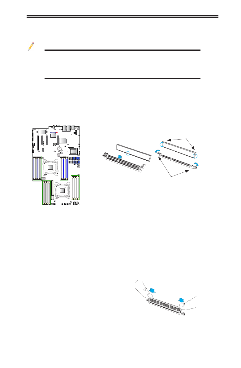
1. Insert the desired number of DIMMs into the memory slots, starting with
P1-DIMMA1. (For best performance, please use the memory modules of the
same type and speed in the same bank.)
2. Push the release tabs outwards on both ends of the DIMM slot to unlock it.
Notches
Release Tabs
3. Align the key of the DIMM module with the receptive point on the DIMM slot.
4. Align the notches on both ends of the module against the receptive points on
the ends of the slot.
5. Use two thumbs together to press the notches on both ends of the module
straight down into the slot until the module snaps into place.
6. Press the release tabs to the locking positions to secure the DIMM module
into the slot.
Removing Memory Modules
Press both notches at the ends of a DIMM module to unlock it. Once it is loosened
from the memory slot, remove the DIMM module from the motherboard.
Press both notches straight
down into the memory slot at
the same time.
2-11
Page 36
X9DRFF-i+/iT+/7+/7T+ Motherboard User’s Manual
Memory Support for the X9DRFF-i+/iT+/7+/7T+ Motherboard
The X9DRFF-i+/iT+/7+/7T+ motherboard supports up to 1 TB of Load Reduced
(LRDIMM), 512 GB of Registered (RDIMM) or 128 GB of Unbuffered (UDIMM)
ECC/Non-ECC DDR3 800/1066/1333/1600/1866 MHz 240-pin 4-channel memory
modules in 16 DIMM slots.
Note: For the latest memory updates, please refer to the Tested Memory
List posted on our website (http://www.supermicro.com/products/mother-
board).
Processor & Memory Module Population Conguration
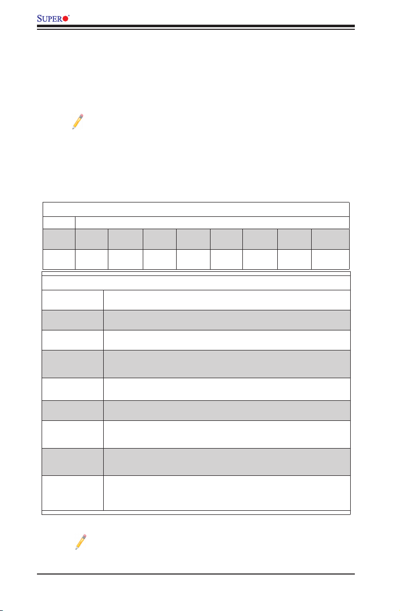
For memory to work properly, follow the tables below for memory installation.
Processors and their Corresponding Memory Modules
CPU# Corresponding DIMM Modules
CPU 1 P1-
DIMMA1
CPU2 P2-
DIMME1
Processor and Memory Module Population for Optimal Performance
Number of
CPUs+DIMMs
1 CPU &
2 DIMMs
1 CPU &
4 DIMMs
1 CPU &
5~8 DIMMs
2 CPUs &
4 DIMMs
2 CPUs &
6 DIMMs
2 CPUs &
8 DIMMs
2 CPUs &
10~16 DIMMs
2 CPUs &
16 DIMMs
P1DIMMB1
P2DIMMF1
CPU1
P1-DIMMA1/P1-DIMMB1
CPU1
P1-DIMMA1/P1-DIMMB1, P1-DIMMC1/P1-DIMMD1
CPU1
P1-DIMMA1/P1-DIMMB1, P1-DIMMC1/P1-DIMMD1 + Any memory pairs in P1DIMMA2/P1-DIMMB2/P1-DIMMC2/P1-DIMMD2 slots
CPU1 + CPU2
P1-DIMMA1/P1-DIMMB1, P2-DIMME1/P2-DIMMF1
CPU1 + CPU2
P1-DIMMA1/P1-DIMMB1/P1-DIMMC1/P1-DIMMD1, P2-DIMME1/P2-DIMMF1
CPU1 + CPU2
P1-DIMMA1/P1-DIMMB1/P1-DIMMC1/P1-DIMMD1, P2-DIMME1/P2-DIMMF1/P2DIMMG1/P2-DIMMH1
CPU1/CPU2
P1-DIMMA1/P1-DIMMB1/P1-DIMMC1/P1-DIMMD1, P2-DIMME1/P2-DIMMF1/P2DIMMG1/P2-DIMMH1 + Any memory pairs in P1, P2 DIMM slots
CPU1/CPU2
P1-DIMMA1/P1-DIMMB1/P1-DIMMC1/P1-DIMMD1, P2-DIMME1/P2-DIMMF1/P2-DIMMG1/P2-DIMMH1,P1-DIMMA2/P1-DIMMB2/P1-DIMMC2/P1-DIMMD2, P2-DIMME2/
P2-DIMMF2/P2-DIMMG2/P2-DIMMH2
P1DIMMC1
P2DIMMG1
(For memory to work properly, please follow the instructions below.)
P1DIMMD1
P2DIMMH1
CPUandMemoryPopulationCongurationTable
P1DIMMA2
P2DIMME2
P1DIMMB2
P2DIMM F2
P1DIMMC2
P2DIMMG2
P1DIMMD2
P2DIMMH2
Notes: 1866 MHz memory speed is dependent on Intel E5-2600v2 CPUs.
For Intel E5-2600(v2) processor support, BIOS version 3.0 or above is
required.
2-12
Page 37
Chapter 2: Installation
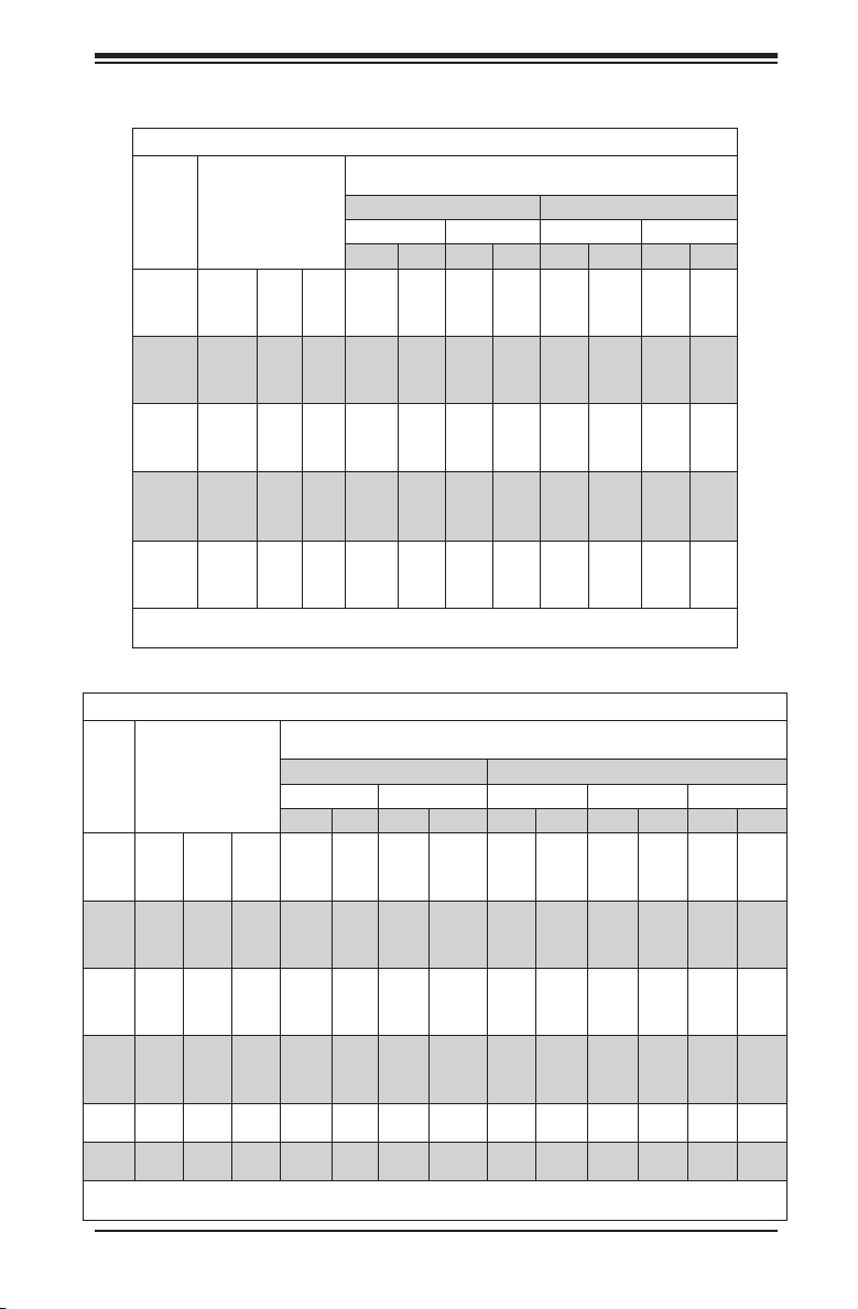
Populating UDIMM (ECC/Non-ECC) Memory Modules
Intel E5-2600(v2) Series Processor UDIMM Memory Support
Ranks
DIMM
& Data
Width
SRx8
Non-
ECC
DRx8
Non-
ECC
SRx16
Non-
ECC
SRx8
ECC
DRx8
ECC
Note: For detailed information on memory support and updates, please refer to the SMC Recommended
Memory List posted on our website at http://www.supermicro.com/support/resources/mem.cfm.
Memory Capacity
Per
Per DIMM
(See the Note below)
1GB 2GB 4GB NA 1066,
2GB 4GB 8GB NA 1066,
512MB 1GB 2GB NA 1066,
1GB 2GB 4GB 1066,
2GB 4GB 8GB 1066,
Speed (MT/s) and Voltage Validated by Slot per Channel (SPC) and
2 Slots Per Channel 3 Slots Per Channel
1DPC 2DPC 1DPC 2DPC
1.35V 1.5V 1.35V 1.5V 1.35V 1.5V 1.35V 1.5v
1333
1333
1333,
1600,
1866
1333,
1600,
1866
1333,
1600,
1866
1066,
1333,
1600,
1866
1066,
1333,
1600,
1866
NA 1066,
NA 1066,
NA 1066,
1066,
1333
1066,
1333
DIMM Per Channel (DPC)
N/A 1066,
1333,
1600
N/A 1066,
1333,
1600
N/A 1066,
1333,
1600
1066,
1066,
1333,
1333
1600
1066,
1066,
1333,
1333
1600
1333,
1600,
1866
1333,
1600,
1866
1333,
1600,
1866
1066,
1333,
1600,
1866
1066,
1333,
1600,
1866
N/A 1066,
N/A 1066,
N/A 1066,
1066,
1333
1066,
1333
1333,
1600
1333,
1600
1333,
1600
1066,
1333,
1600
1066,
1333,
1600
Populating RDIMM (ECC) Memory Modules
Intel E5-2600(v2) Series Processor RDIMM Memory Support
Ranks
DIMM
Width
QRx4 8GB 16GB 32GB 800 800
QRx8 4GB 8GB 16GB 800 800
Note: For detailed information on memory support and updates, please refer to the SMC Recommended Memory List posted on
our website at http://www.supermicro.com/support/resources/mem.cfm.
Memory Capacity
Per
&
Data
SRx8 1GB 2GB 4GB 1066,
DRx8 2GB 4GB 8GB 1066,
SRx4 2GB 4GB 8GB 1066,
DRx4 4GB 8GB 16GB 1066,
Per DIMM
(See the Note Below)
Speed (MT/s) and Voltage Validated by Slot per Channel (SPC) and DIMM Per Channel
1.35V 1.5V 1.35V 1.5V 1.35V 1.5V 1.35V 1.5V 1.35V 1.5v
1333
1333
1333
1333
(DPC)
2 Slots Per Channel 3 Slots Per Channel
1DPC 2DPC 1 DPC 2DPC 3DPC
1066,
1066,
1066,
1066,
1066,
1066,
1066,
1333,
1333
1600,
1866
1066,
1333,
1600,
1866
1066,
1333,
1600,
1866
1066,
1333,
1600,
1866
1066
1066
1333,
1600
1066,
1066,
1333
1333,
1600
1066,
1066,
1333
1333,
1600
1066,
1066,
1333
1333,
1600
800 800 800 800,
800 800 800 800,
1333
1066,
1333
1066,
1333
1066,
1333
1333,
1333
1600,
1866
1066,
1066,
1333,
1333
1600,
1866
1066,
1066,
1333,
1333
1600,
1866
1066,
1066,
1333,
1333
1600,
1866
800 800 N/A N/A
1066
800 800 N/A N/A
1066
1333,
1600
1066,
1333,
1600
1066,
1333,
1600
1066,
1333,
1600
800 800,
800 800,
800 800,
800 800,
1066
1066
1066
1066
2-13
Page 38
X9DRFF-i+/iT+/7+/7T+ Motherboard User’s Manual
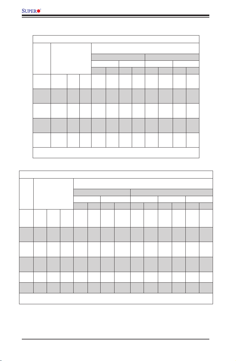
Populating UDIMM (ECC/Non-ECC) Memory Modules
Intel E5-2600 Series Processor UDIMM Memory Support
Ranks
DIMM
& Data
Width
SRx8
Non-
ECC
DRx8
Non-
ECC
SRx16
Non-
ECC
SRx8
ECC
DRx8
ECC
Note: For detailed information on memory support and updates, please refer to the SMC Recommended
Memory List posted on our website at http://www.supermicro.com/support/resources/mem.cfm.
Memory Capacity
Per
Per DIMM
(See the Note below)
1GB 2GB 4GB NA 1066,
2GB 4GB 8GB NA 1066,
512MB 1GB 2GB NA 1066,
1GB 2GB 4GB 1066,
2GB 4GB 8GB 1066,
Speed (MT/s) and Voltage Validated by Slot per Channel (SPC) and
2 Slots Per Channel 3 Slots Per Channel
1DPC 2DPC 1DPC 2DPC
1.35V 1.5V 1.35V 1.5V 1.35V 1.5V 1.35V 1.5v
1333
1333
1333
1333
1333
1066,
1333
1066,
1333
NA 1066,
NA 1066,
NA 1066,
1066 1066,
1066 1066,
DIMM Per Channel (DPC)
N/A 1066,
1333
N/A 1066,
1333
N/A 1066,
1333
1066 1066,
1333
1066 1066,
1333
1333,
1333,
1333
1333,
1333,
N/A 1066,
1333
N/A 1066,
1333
N/A 1066,
1333
1066,
1066,
1333
1333
1066,
1066,
1333
1333
Populating RDIMM (ECC) Memory Modules
Intel E5-2600 Series Processor RDIMM Memory Support
Ranks
Memory Capacity
Per
DIMM
&
Data
Width
SRx8 1GB 2GB 4GB 1066,
DRx8 2GB 4GB 8GB 1066,
SRx4 2GB 4GB 8GB 1066,
DRx4 4GB 8GB 16GB 1066,
QRx4 8GB 16GB 32GB 800 1066 800 800 800 1066 800 800 N/A N/A
Per DIMM
(See the Note Below)
Speed (MT/s) and Voltage Validated by Slot per Channel (SPC) and DIMM Per Channel
2 Slots Per Channel 3 Slots Per Channel
1DPC 2DPC 1 DPC 2DPC 3DPC
1.35V 1.5V 1.35V 1.5V 1.35V 1.5V 1.35V 1.5V 1.35V 1.5v
1066,
1066,
1333
1333
1333
1333
1333,
1600
1066,
1333,
1600
1066,
1333,
1600
1066,
1333,
1600
1333
1066,
1333
1066,
1333
1066,
1333
1066,
1333,
1600
1066,
1333,
1600
1066,
1333,
1600
1066,
1333,
1600
1066,
1333
1066,
1333
1066,
1333
1066,
1333
(DPC)
1066,
1333,
1600
1066,
1333,
1600
1066,
1333,
1600
1066,
1333,
1600
1066,
1333
1066,
1333
1066,
1333
1066,
1333
1066,
1333,
1600
1066,
1333,
1600
1066,
1333,
1600
1066,
1333,
1600
N/A 800,
N/A 800,
N/A 800,
N/A 800,
1066
1066
1066
1066
QRx8 4GB 8GB 16GB 800 1066 800 800 800 1066 800 800 N/A N/A
Note: For detailed information on memory support and updates, please refer to the SMC Recommended Memory List posted on
our website at http://www.supermicro.com/support/resources/mem.cfm.
2-14
Page 39
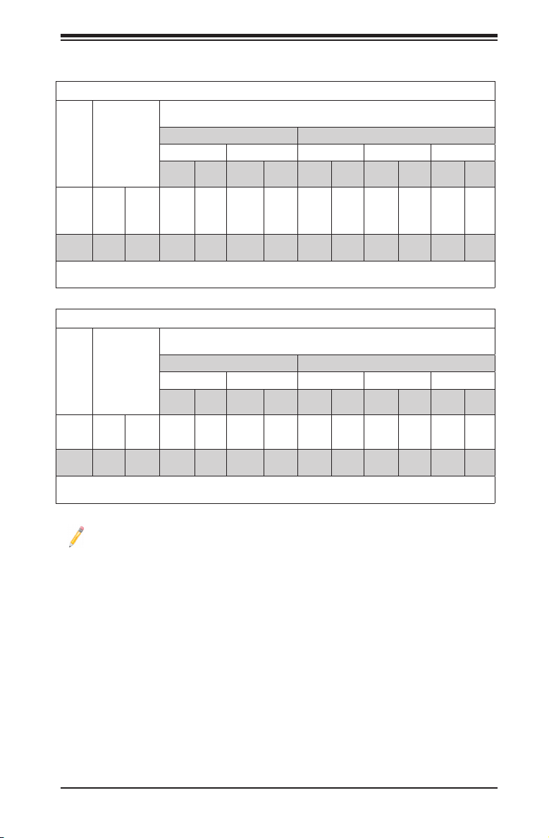
Chapter 2: Installation
Populating LRDIMM (ECC) Memory Modules
Intel E5-2600(v2) Series Processor LRDIMM Memory Support
Ranks
DIMM
Data
Width
QRx4
(DDP)
8Rx4
(QDP)
Note: For detailed information on memory support and updates, please refer to the SMC Recommended Memory
List posted on our website at http://www.supermicro.com/support/resources/mem.cfm.
Ranks
DIMM
Data
Width
QRx4
(DDP)
Memory
Per
Capacity
Per DIMM
&
(See the Note
Below)
16GB 32GB 1066,
32GB 64GB 1066 1066 1066 1066 1066 1066 1066 1066 1066 1066
Speed (MT/s) and Voltage Validated by Slot per Channel (SPC) and DIMM Per
2 Slots Per Channel 3 Slots Per Channel
1DPC 2DPC 1DPC 2DPC 3DPC
1.35V 1.5V 1.35V 1.5V 1.35V 1.5V 1.35V 1.5V 1.35V 1.5V
1066,
1333,
1600,
1866
1066,
1333,
1600
1333,
1600
1066,
1333,
1600
Channel (DPC)
1066,
1066,
1333,
1333,
1600
1600,
1866
1066,
1333,
1600
1066,
1333,
1600
Intel E5-2600 Series Processor LRDIMM Memory Support
Memory
Per
Capacity
Per DIMM
&
(See the Note
Below)
16GB 32GB 1066 1066,
Speed (MT/s) and Voltage Validated by Slot per Channel (SPC) and DIMM Per
2 Slots Per Channel 3 Slots Per Channel
1DPC 2DPC 1DPC 2DPC 3DPC
1.35V 1.5V 1.35V 1.5V 1.35V 1.5V 1.35V 1.5V 1.35V 1.5V
1066 1066,
1333
1333
Channel (DPC)
1066 1066,
1333
1066 1066,
1333
1066 1066
1066 1066
QRx8
8GB 16GB 1066 1066,
(QDP)
Note: For detailed information on memory support and updates, please refer to the SMC Recommended Memory
List posted on our website at http://www.supermicro.com/support/resources/mem.cfm.
1333
1066 1066,
1333
1066 1066 1066 1066 1066 1066
Other Important Notes and Restrictions
•For the memory modules to work properly, please install DIMM modules of the same
type, same speed and same operating frequency on the motherboard. Mixing of
RDIMMs, UDIMMs or LRDIMMs is not allowed. Do not install both ECC and Non-ECC
memory modules on the same motherboard.
•Using DDR3 DIMMs with different operating frequencies is not allowed. All channels
in a system will run at the lowest common frequency.
2-15
Page 40
X9DRFF-i+/iT+/7+/7T+ Motherboard User’s Manual
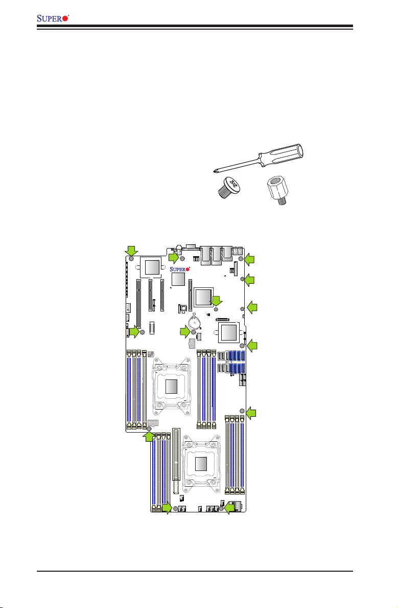
2-5 Motherboard Installation
All motherboards have standard mounting holes to t different types of chassis.
Make sure that the locations of all the mounting holes for both motherboard and
chassis match. Although a chassis may have both plastic and metal mounting fas-
teners, metal ones are highly recommended because they ground the motherboard
to the chassis. Make sure that the metal standoffs click in or are screwed in tightly.
Then use a screwdriver to secure the motherboard onto the motherboard tray.
Tools Needed
•Phillips Screwdriver
•Pan head screws (13 pieces)
•Standoffs (13 pieces, if needed)
Location of Mounting Holes
There are thirteen (13) mounting holes on this motherboard indicated by the arrows.
JPL1
JPME1
JPME2
JNMI1
JWD1
JRST1
JI2C2
JI2C1
JL1
USB2
COM1
FAN9
JPI2C1
P1 DIMMA2
P1 DIMMB1
P1 DIMMA1
FAILURE_LED1
Intel
LAN CTRL
PCH SLOT2 PCI-E 2.0 X4 (IN X8)
CPU1 SLOT3 PCI-E 3.0 X8
CPU1 SLOT1 PCI-E 3.0 X16
BMC_HB_LED1
JPP1
JPP2
JITP1
XDP-CPU
P1 DIMMB2
JPW3
CPU1
CLOSE 1st
P2 DIMMH2
P2 DIMMH1
P2 DIMMG2
JPW2
P2 DIMMG1
UID_LED1
UID_SW1
VGA
PWR_SW1
JPB1
JP7
X9DRFF-i(T)+_7(T)+
Rev.1.02
Nuvotun
CPU2 SLOT4 PCI-E 3.0 X8
BMC
CPLD1
JBT1
BIOS
JBAT1
JPW1
OPEN 1st
P1 DIMMC2
P1 DIMMC1
P1 DIMMD2
P1 DIMMD1
SXB1_2
SXB1 CPU2 PCI-E 3.0 X16 + x16
CLOSE 1st
JP6
Intel PCH
BBU1
CPU2
LAN2
SAS_HB_LED1
HDD_FAULT
_LED1
LAN1
IPMI_LAN
_LED1
SAS_ERR_LED2
SAS_ERR_LED1
TFM1
SAS CTRL
(SAS #0-7)
#4
#2
#3
#5
(SATA #0-5)
HDD_ACT
LSI 2208
#0
#1
P2 DIMMF2
JPG1
JPS1
#5
#4
JSD1
P2 DIMMF1
USB1
JTPM1
#6
#0
6-SGPIO2
6-SGPIO1
P2 DIMME2
#3#1#7
#2
T-SGPIO1
USB0
LSI_UART2
LSI_UART1
T-SGPIO2
P2 DIMME1
OPEN 1st
SXB1_1
FAN8
FAN6
FAN7
FAN1
HDD_PWR2
FAN3
FAN4
FAN5
HDD_PWR1
FAN2
Warning: 1) To avoid damaging the motherboard and its components, please do
not use a force greater than 8 lb/inch on each mounting screw during motherboard
installation. 2) Some components are very close to the mounting holes. Please take
precautionary measures to prevent damage to these components when installing the
motherboard to the chassis.
2-16
Page 41
Chapter 2: Installation
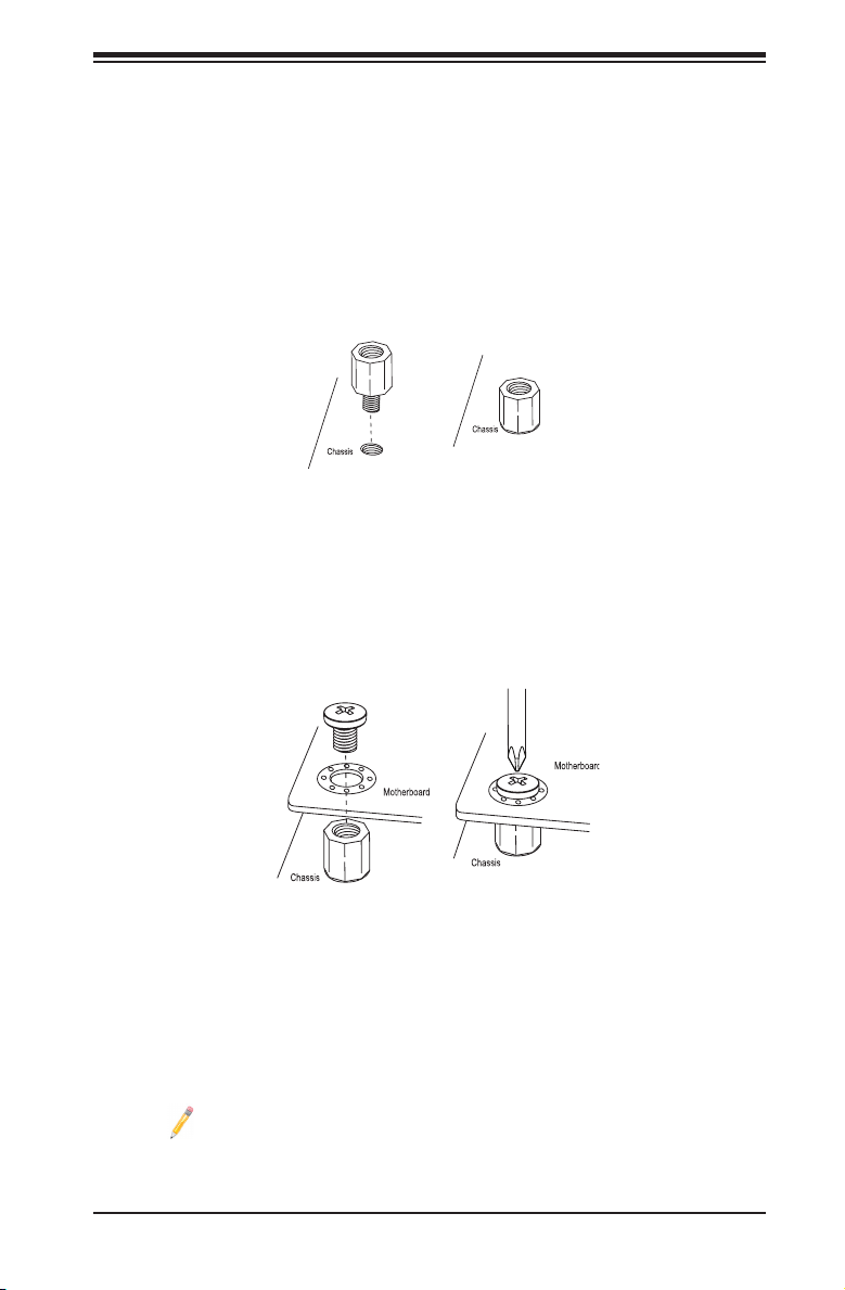
Installing the Motherboard
1. Locate the mounting holes on the motherboard.
2. Locate the matching mounting holes on the chassis. Align the mounting holes
on the motherboard against the mounting holes on the chassis.
3. Install standoffs in the chassis as needed.
4. Install the motherboard into the chassis carefully to avoid damaging mother-
board components.
5. Using the Phillips screwdriver, insert a Pan head #6 screw into a mounting
hole on the motherboard and its matching mounting hole on the chassis.
6. Repeat Step 5 to insert #6 screws into all mounting holes.
7. Make sure that the motherboard is securely placed in the chassis.
Note: Images displayed are for illustration only. Your chassis or compo-
nents might look different from those shown in this manual.
2-17
Page 42
X9DRFF-i+/iT+/7+/7T+ Motherboard User’s Manual
1
2
3
4
5
6
7
2-6 Control Panel Connectors and I/O Ports
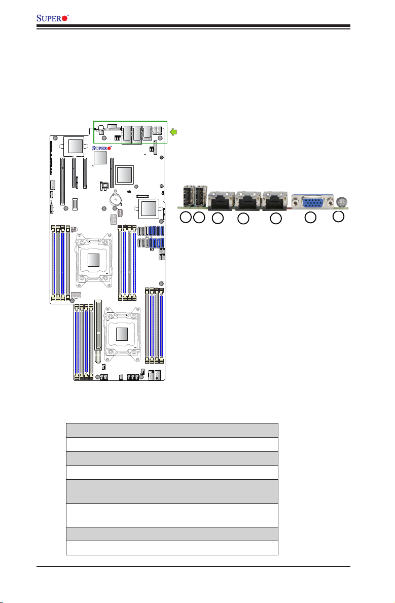
The I/O ports are color coded in conformance with the PC 99 specication. See
the picture below for the colors and locations of the various I/O por ts.
Back Panel Connectors and I/O Ports
FAILURE_LED1
Intel
JPL1
LAN CTRL
JPME1
JPME2
PCH SLOT2 PCI-E 2.0 X4 (IN X8)
CPU1 SLOT1 PCI-E 3.0 X16
JITP1
P1 DIMMA2
P1 DIMMB1
P1 DIMMB2
JPW3
JPW2
P2 DIMMG1
CPU1 SLOT3 PCI-E 3.0 X8
JPP1
JPP2
XDP-CPU
CPU1
CLOSE 1st
P2 DIMMH2
P2 DIMMH1
P2 DIMMG2
JNMI1
JWD1
JRST1
JI2C2
JI2C1
JL1
USB2
COM1
FAN9
JPI2C1
P1 DIMMA1
UID_LED1
UID_SW1
VGA
PWR_SW1
JPB1
X9DRFF-i(T)+_7(T)+
Rev.1.02
Nuvotun
CPU2 SLOT4 PCI-E 3.0 X8
BMC
BMC_HB_LED1
CPLD1
JBT1
BIOS
JBAT1
JPW1
OPEN 1st
P1 DIMMD2
P1 DIMMD1
SXB1_2
SXB1 CPU2 PCI-E 3.0 X16 + x16
CLOSE 1st
SXB1_1
FAN8
FAN6
FAN7
JP6
JP7
Intel PCH
BBU1
P1 DIMMC2
P1 DIMMC1
CPU2
FAN5
LAN2
SAS_HB_LED1
HDD_FAULT
_LED1
OPEN 1st
FAN4
LAN1
IPMI_LAN
_LED1
SAS_ERR_LED2
SAS_ERR_LED1
TFM1
(SAS #0-7)
#4
#2
#3
#5
(SATA #0-5)
FAN1
FAN3
FAN2
HDD_ACT
LSI 2208
SAS CTRL
#0
#1
P2 DIMMF2
HDD_PWR2
JPG1
JPS1
#5
#4
JSD1
P2 DIMMF1
USB1
JTPM1
#6
#0
6-SGPIO2
6-SGPIO1
P2 DIMME2
T-SGPIO1
USB0
LSI_UART2
LSI_UART1
#3#1#7
#2
T-SGPIO2
P2 DIMME1
HDD_PWR1
BackPanelI/OPortLocationsandDenitions
X9DRFF-i+/iT+/7+/7T+ I/O Back Panel
1. Back Panel USB Port 1
2. Back Panel USB Port 2
3. IPMI LAN
4. 10-Gigabit LAN 1 (for X9DRFF-iT+/-7T+),
1-Gigabit LAN 1 (X9DRFF-i+/-7+)
5. 10-Gigabit LAN 2 (X9DRFF-iT+/-7T+),
1-Gigabit LAN 2 (X9DRFF-i+/-7+)
6. VGA
7. Power Switch
2-18
Page 43
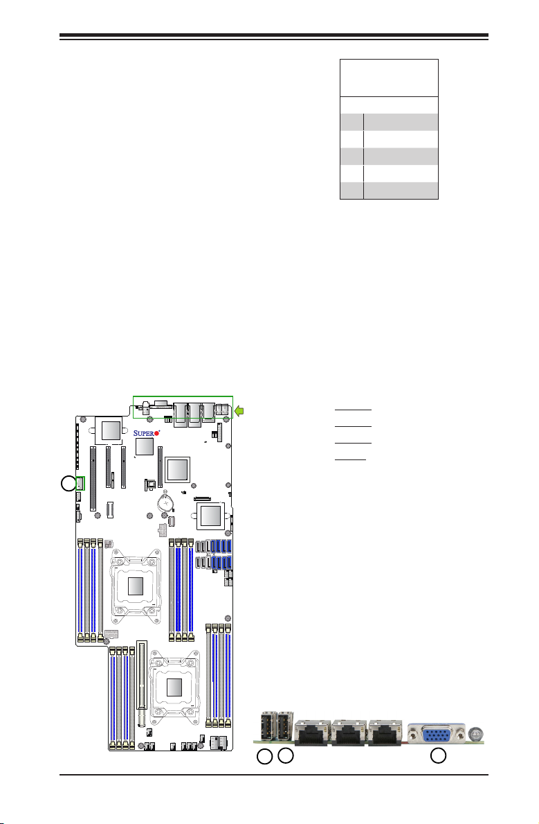
Chapter 2: Installation
1
2
3
4
Universal Serial Bus (USB)
Two Universal Serial Bus ports (USB0,
USB1), located on the I/O backplane,
provide rear USB support. In addi-
tion, USB2 (JUSB2), located next to
the 4-pin JIPMB1 connector, provides
front USB support. (USB Cables are
not included). See the table on the
right for pin denitions.
Video Connection
A Video (VGA) port is located next to
the LAN Port 2 on the I/O backplane.
Refer to the layout below for the
location.
LAN2
LAN1
VGA
JPB1
JP6
JP7
X9DRFF-i(T)+_7(T)+
Rev.1.02
CPU2 SLOT4 PCI-E 3.0 X8
Intel PCH
SAS_ERR_LED2
SAS_ERR_LED1
SAS_HB_LED1
JBT1
BIOS
JBAT1
HDD_FAULT
_LED1
BBU1
JPW1
P1 DIMMC2
P1 DIMMC1
P1 DIMMD2
P1 DIMMD1
SXB1 CPU2 PCI-E 3.0 X16 + x16
CPU2
CLOSE 1st
TFM1
(SAS #0-7)
#4
#5
(SATA #0-5)
IPMI_LAN
HDD_ACT
_LED1
LSI 2208
SAS CTRL
#0
#2
#1
#3
P2 DIMMF2
USB1
JPG1
JPS1
#5
#6
#4
6-SGPIO1
JSD1
P2 DIMMF1
JTPM1
#0
6-SGPIO2
T-SGPIO1
P2 DIMME2
USB0
LSI_UART2
LSI_UART1
#3#1#7
#2
T-SGPIO2
P2 DIMME1
JPL1
JPME1
JPME2
JNMI1
JWD1
JRST1
JI2C2
JI2C1
JL1
USB2
COM1
FAN9
JPI2C1
P1 DIMMA1
P1 DIMMA2
P1 DIMMB1
FAILURE_LED1
Intel
LAN CTRL
PCH SLOT2 PCI-E 2.0 X4 (IN X8)
CPU1 SLOT3 PCI-E 3.0 X8
CPU1 SLOT1 PCI-E 3.0 X16
BMC_HB_LED1
JPP1
JPP2
JITP1
XDP-CPU
P1 DIMMB2
JPW3
CPU1
CLOSE 1st
P2 DIMMH2
P2 DIMMH1
P2 DIMMG2
JPW2
P2 DIMMG1
UID_LED1
UID_SW1
Nuvotun
BMC
CPLD1
SXB1_2
PWR_SW1
OPEN 1st
Backplane USB 0/1
& FP USB 2
PinDenitions
Pin# Denition
1 +5V
2 PO-
3 PO+
4 Ground
5 NA
1. USB0
2. USB1
3. USB2
4. VGA
OPEN 1st
SXB1_1
FAN8
FAN6
FAN7
FAN1
HDD_PWR2
FAN3
FAN4
FAN5
HDD_PWR1
FAN2
2-19
Page 44
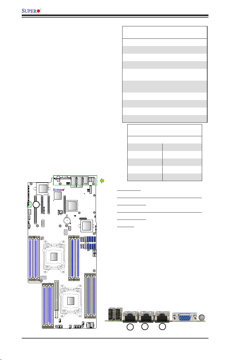
X9DRFF-i+/iT+/7+/7T+ Motherboard User’s Manual
1
2
3
4
Ethernet Ports
Two Ethernet ports (LAN1, LAN2) are
located on the I/O backplane. These
Ethernet ports support 10G LAN con-
nections on the X9DRFF-iT+/7T+, and
1G LAN connections on the X9DRFF-
i+/7+. In addition, an IPMI LAN port
is also located on the backplane.
All these ports accept RJ45 cables.
Please refer to the LED Indicator Sec-
tion for LAN LED information.
Serial Port
A serial port (COM1) is located next to
the IPMI LAN port on the motherboard.
COM1 provides serial connection sup-
port. See the table on the right for pin
denitions.
LAN2
VGA
JPB1
JP6
JP7
X9DRFF-i(T)+_7(T)+
Rev.1.02
CPU2 SLOT4 PCI-E 3.0 X8
Intel PCH
JBT1
BIOS
JBAT1
BBU1
JPW1
P1 DIMMC2
P1 DIMMC1
P1 DIMMD2
P1 DIMMD1
CPU2
CLOSE 1st
SAS_HB_LED1
HDD_FAULT
_LED1
LAN1
IPMI_LAN
SAS_ERR_LED2
SAS_ERR_LED1
TFM1
(SAS #0-7)
#4
#3
#5
(SATA #0-5)
HDD_ACT
_LED1
LSI 2208
SAS CTRL
#0
#2
#1
P2 DIMMF2
JPG1
#5
#4
USB1
JPS1
JTPM1
#6
#0
6-SGPIO2
6-SGPIO1
JSD1
P2 DIMMF1
P2 DIMME2
#2
T-SGPIO1
USB0
LSI_UART2
LSI_UART1
#3#1#7
T-SGPIO2
P2 DIMME1
JPL1
JPME1
JPME2
JNMI1
CPU1 SLOT1 PCI-E 3.0 X16
JWD1
JRST1
JI2C2
JI2C1
JL1
USB2
COM1
FAN9
JPI2C1
P1 DIMMA2
P1 DIMMB1
P1 DIMMA1
FAILURE_LED1
UID_LED1
UID_SW1
Intel
LAN CTRL
Nuvotun
PCH SLOT2 PCI-E 2.0 X4 (IN X8)
CPU1 SLOT3 PCI-E 3.0 X8
BMC
BMC_HB_LED1
JPP1
JPP2
JITP1
XDP-CPU
P1 DIMMB2
JPW3
CPU1
CLOSE 1st
P2 DIMMH2
P2 DIMMH1
P2 DIMMG2
JPW2
P2 DIMMG1
PWR_SW1
CPLD1
OPEN 1st
SXB1_2
SXB1 CPU2 PCI-E 3.0 X16 + x16
LAN Ports
PinDenition
Pin# Denition
1 P2V5SB 10 SGND
2 TD0+ 11 Act LED
3 TD0- 12 P3V3SB
4 TD1+ 13 Link 100 LED (Yel-
5 TD1- 14 Link 1000 LED
low, +3V3SB)
(Yellow, +3V3SB)
6 TD2+ 15 Ground
7 TD2- 16 Ground
8 TD3+ 17 Ground
9 TD3- 18 Ground
Serial Port (COM1)
PinDenitions
Pin # Denition Pin # Denition
1 DCD 6 DSR
2 RXD 7 RTS
3 TXD 8 CTS
4 DTR 9 RI
5 Ground 10 N/A
1. IPMI LAN
2. LAN1(10G LAN: X9DRFF-iT+/7T+, GLAN:
X9DRFF-i+/7+)
3. LAN2 (10G LAN: X9DRFF-iT+/7T+, GLAN:
X9DRFF-i+/7+)
4. COM1
OPEN 1st
SXB1_1
FAN8
FAN6
FAN7
FAN1
HDD_PWR2
FAN3
FAN4
FAN5
HDD_PWR1
FAN2
2-20
Page 45
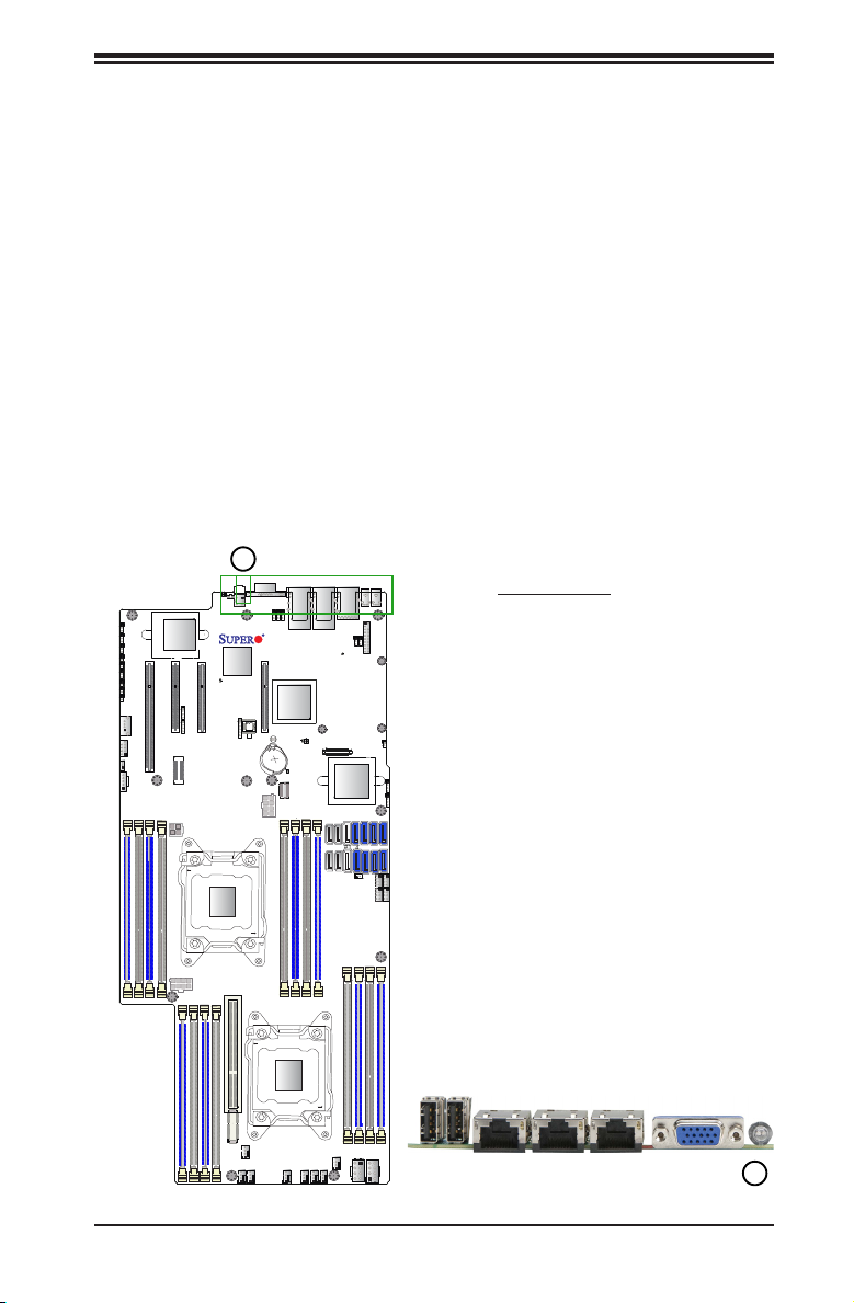
LAN2
LAN1
1
1
Power Switch
A power switch (PWR_SW1) is located next
to the VGA port on the motherboard. Refer
to the layout below for the location.
Chapter 2: Installation
JPL1
JPME1
JPME2
JNMI1
JWD1
JRST1
JI2C2
JI2C1
JL1
USB2
COM1
FAN9
JPI2C1
P1 DIMMA2
P1 DIMMA1
P1 DIMMB1
CPU1 SLOT1 PCI-E 3.0 X16
FAILURE_LED1
UID_LED1
UID_SW1
Intel
LAN CTRL
Nuvotun
PCH SLOT2 PCI-E 2.0 X4 (IN X8)
CPU1 SLOT3 PCI-E 3.0 X8
BMC
BMC_HB_LED1
JPP1
JPP2
JITP1
XDP-CPU
P1 DIMMB2
JPW3
CPU1
CLOSE 1st
SXB1_2
P2 DIMMH2
P2 DIMMH1
P2 DIMMG2
JPW2
P2 DIMMG1
SXB1_1
VGA
PWR_SW1
JPB1
JP6
JP7
X9DRFF-i(T)+_7(T)+
Rev.1.02
CPU2 SLOT4 PCI-E 3.0 X8
Intel PCH
CPLD1
SAS_HB_LED1
JBT1
BIOS
JBAT1
HDD_FAULT
_LED1
BBU1
JPW1
OPEN 1st
P1 DIMMC2
P1 DIMMC1
P1 DIMMD2
P1 DIMMD1
SXB1 CPU2 PCI-E 3.0 X16 + x16
CPU2
CLOSE 1st
FAN8
FAN4
FAN6
FAN5
FAN7
SAS_ERR_LED2
SAS_ERR_LED1
(SATA #0-5)
OPEN 1st
FAN3
FAN2
TFM1
(SAS #0-7)
#4
#5
IPMI_LAN
HDD_ACT
_LED1
LSI 2208
SAS CTRL
#0
#2
#1
#3
P2 DIMMF2
FAN1
HDD_PWR2
JPG1
JPS1
#5
#4
JSD1
P2 DIMMF1
USB1
JTPM1
#6
#0
6-SGPIO2
6-SGPIO1
T-SGPIO1
P2 DIMME2
USB0
LSI_UART2
LSI_UART1
#3#1#7
#2
T-SGPIO2
P2 DIMME1
HDD_PWR1
1. Power Switch
2-21
Page 46
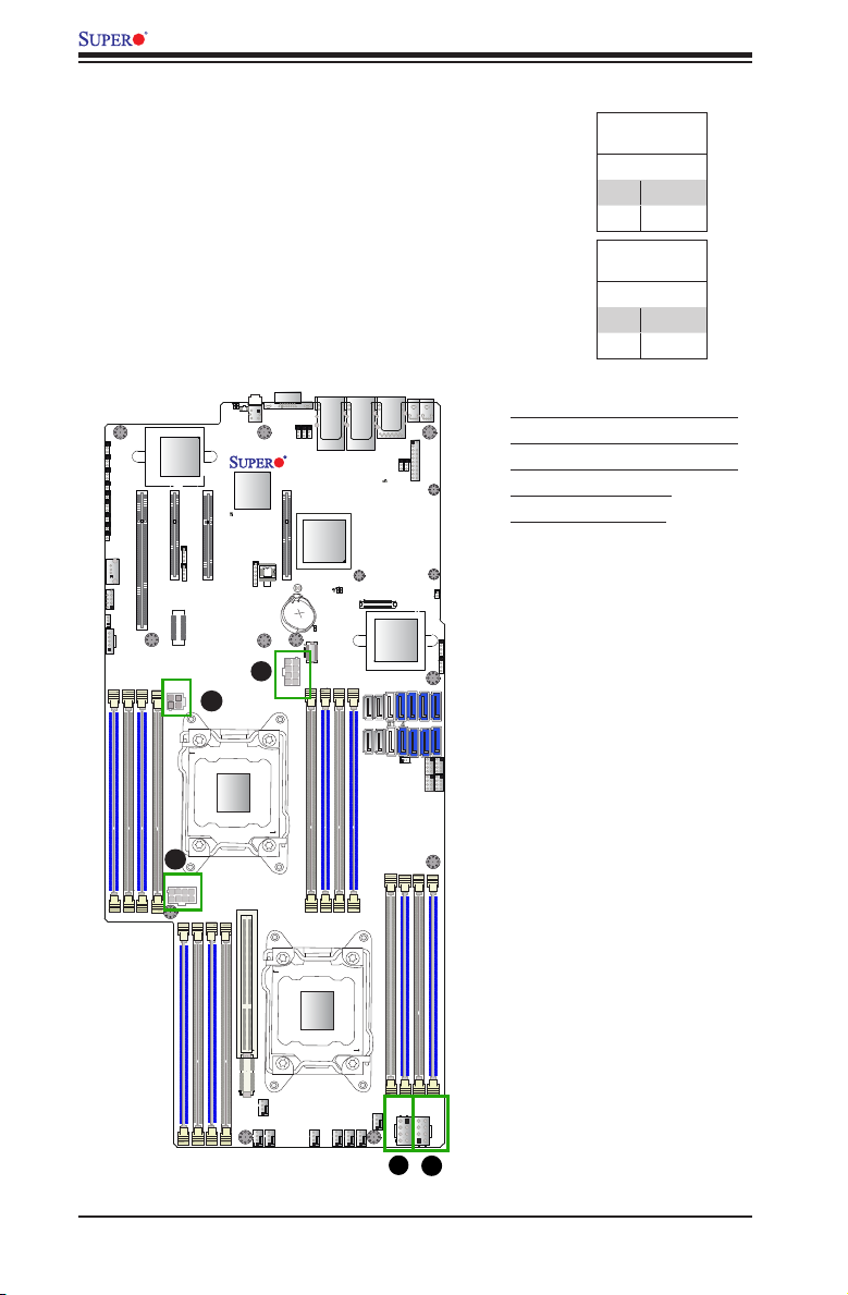
X9DRFF-i+/iT+/7+/7T+ Motherboard User’s Manual
D
E
2-7 Connecting Cables
Two 8-pin power connectors (JPW1/JPW2) and a
4-pin power connector (JPW3) are located on the
motherboard. In addition, two 8-pin power connectors
(HDD_PWR1/2) are also located onboard to provide
power supply to hard disk drive devices. These power
connectors meet the SSI EPS 12V specication. Be sure
to connect the all the power connectors to your power
supply to provide adequate power to the system. See
the table on the right for pin denitions.
LAN2
LAN1
JPB1
JP6
JP7
X9DRFF-i(T)+_7(T)+
Rev.1.02
Intel PCH
SAS_ERR_LED2
SAS_ERR_LED1
SAS_HB_LED1
JBT1
BBU1
HDD_FAULT
_LED1
TFM1
#4
#5
(SATA #0-5)
IPMI_LAN
HDD_ACT
_LED1
LSI 2208
SAS CTRL
(SAS #0-7)
#0
#2
#1
#3
JPG1
#4
JPS1
#5
JSD1
USB1
JTPM1
#6
#0
6-SGPIO2
6-SGPIO1
T-SGPIO1
USB0
LSI_UART2
LSI_UART1
#3#1#7
#2
T-SGPIO2
JPL1
JPME1
JPME2
JNMI1
CPU1 SLOT1 PCI-E 3.0 X16
JWD1
JRST1
JI2C2
JI2C1
JL1
USB2
COM1
FAN9
JPI2C1
P1 DIMMA2
P1 DIMMB1
P1 DIMMA1
FAILURE_LED1
UID_LED1
UID_SW1
PWR_SW1
Intel
LAN CTRL
CPU1 SLOT3 PCI-E 3.0 X8
BMC_HB_LED1
JPP1
JPP2
XDP-CPU
C
CPU1
CLOSE 1st
Nuvotun
BMC
CPLD1
PCH SLOT2 PCI-E 2.0 X4 (IN X8)
JITP1
P1 DIMMB2
JPW3
VGA
CPU2 SLOT4 PCI-E 3.0 X8
BIOS
JBAT1
A
JPW1
12V 8-pin PWR
PinDenitions
Pins Denition
1- 4 Ground
5-8 +12V
12V 4-pin PWR
PinDenitions
Pins Denition
1/2 Ground
3/4 +12V
(Required)
A. JPW1 (8-pin Power Connector)
B. JPW2 (8-pin Power Connector)
C. JPW3 (4-pin Power Connector)
D. HDD_ PWR1 (8-pin)
E. HDD_PWR2 (8-pin)
B
JPW2
P2 DIMMG1
P2 DIMMH1
P2 DIMMG2
P2 DIMMH2
OPEN 1st
P1 DIMMC2
P1 DIMMC1
P1 DIMMD2
P1 DIMMD1
SXB1_2
SXB1 CPU2 PCI-E 3.0 X16 + x16
CPU2
CLOSE 1st
SXB1_1
FAN8
FAN6
FAN5
FAN7
OPEN 1st
FAN4
P2 DIMMF1
P2 DIMME2
P2 DIMMF2
P2 DIMME1
FAN1
HDD_PWR2
FAN3
FAN2
HDD_PWR1
2-22
Page 47
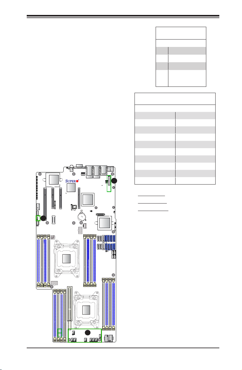
Chapter 2: Installation
Fan Headers
This motherboard has eight 4-pin
(Fan1~Fan8), and one 3-pin (Fan9)
system/CPU/cooling fan headers on the
motherboard. The 4-pin fan headers are
backward compatible with the traditional
3-pin fans. However, fan speed control
is only available on 4-pin fans via IPMI
rmware management. See the table on
the right for pin denitions.
TPM Header/Port 80
A Trusted Platform Module/Port 80 header,
located at JTPM1, provides TPM support
and Port 80 connection. Use this header
to enhance system performance and data
security. See the table on the right for pin
denitions.
LAN2
VGA
JPB1
JP6
JP7
X9DRFF-i(T)+_7(T)+
Rev.1.02
CPU2 SLOT4 PCI-E 3.0 X8
Intel PCH
SAS_ERR_LED2
SAS_HB_LED1
JBT1
JBAT1
HDD_FAULT
_LED1
BBU1
JPW1
P1 DIMMC2
P1 DIMMC1
P1 DIMMD2
P1 DIMMD1
CPU2
CLOSE 1st
LAN1
IPMI_LAN
_LED1
SAS_ERR_LED1
TFM1
LSI 2208
SAS CTRL
(SAS #0-7)
#4
#2
#3
#5
(SATA #0-5)
HDD_ACT
JPG1
JPS1
#0
#5
#1
#4
JSD1
P2 DIMMF1
P2 DIMMF2
USB1
JTPM1
#6
#0
6-SGPIO2
6-SGPIO1
P2 DIMME2
USB0
C
#3#1#7
#2
T-SGPIO1
LSI_UART2
LSI_UART1
T-SGPIO2
P2 DIMME1
JPL1
JPME1
JPME2
JNMI1
CPU1 SLOT1 PCI-E 3.0 X16
JWD1
JRST1
JI2C2
JI2C1
JL1
USB2
COM1
FAN9
B
JPI2C1
P1 DIMMA2
P1 DIMMB1
P1 DIMMA1
FAILURE_LED1
UID_LED1
UID_SW1
Intel
LAN CTRL
Nuvotun
PCH SLOT2 PCI-E 2.0 X4 (IN X8)
CPU1 SLOT3 PCI-E 3.0 X8
BMC
BMC_HB_LED1
JPP1
CPLD1
JPP2
JITP1
XDP-CPU
P1 DIMMB2
JPW3
CPU1
CLOSE 1st
SXB1_2
P2 DIMMH2
P2 DIMMH1
P2 DIMMG2
JPW2
P2 DIMMG1
PWR_SW1
BIOS
OPEN 1st
SXB1 CPU2 PCI-E 3.0 X16 + x16
Fan Header
PinDenitions
Pin# Denition
1 Ground
2 +12V
3 Tachometer
4 PWR Modulation
(Available for 4-pin
fans only)
TPM/Port 80 Header
PinDenitions
Pin # Denition Pin # Denition
1 LCLK 2 GND
3 LFRAME# 4 <(KEY)>
5 LRESET# 6 +5V (X)
7 LAD 3 8 LAD 2
9 +3.3V 10 LAD1
11 LAD0 12 GND
13 SMB_CLK4 14 SMB_DAT4
15 +3V_DUAL 16 SERIRQ
17 GND 18 CLKRUN# (X)
19 LPCPD# 20 LDRQ# (X)
A. Fan1-Fan8
B. Rear_Fan 1
C. TPM/Port 80
SXB1_1
OPEN 1st
FAN8
FAN6
FAN7
FAN1
HDD_PWR2
FAN3
A
FAN4
FAN5
HDD_PWR1
FAN2
2-23
Page 48
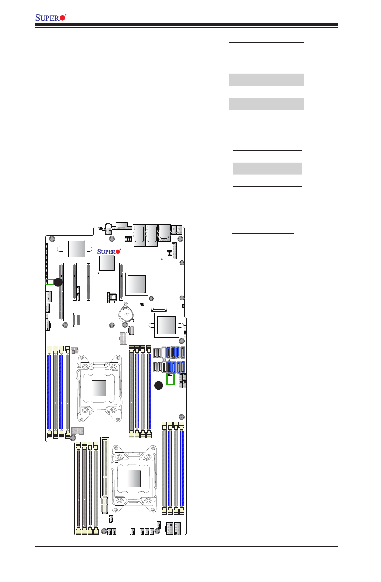
X9DRFF-i+/iT+/7+/7T+ Motherboard User’s Manual
SATA DOM Power Connector
A power connector for SATA DOM
(Disk_On_Module) devices is located at
JSD1. Connect an appropriate cable here
to provide power support for your SATA
DOM devices.
Chassis Intrusion
A Chassis Intrusion header is located at
JL1 on the motherboard. Attach an ap-
propriate cable from the chassis to alert
you when the chassis is opened.
LAN2
LAN1
VGA
JPB1
JP6
JP7
X9DRFF-i(T)+_7(T)+
Rev.1.02
Intel PCH
SAS_ERR_LED2
SAS_ERR_LED1
SAS_HB_LED1
JBT1
HDD_FAULT
_LED1
BBU1
JPW1
IPMI_LAN
_LED1
TFM1
LSI 2208
SAS CTRL
(SAS #0-7)
#4
#2
#3
#5
(SATA #0-5)
A
HDD_ACT
JPG1
JPS1
#0
#5
#1
#4
JSD1
USB1
JTPM1
#6
#0
6-SGPIO2
6-SGPIO1
USB0
#3#1#7
#2
T-SGPIO2
T-SGPIO1
JPL1
JPME1
JPME2
JNMI1
CPU1 SLOT1 PCI-E 3.0 X16
JWD1
JRST1
JI2C2
JI2C1
JL1
B
USB2
COM1
FAN9
JPI2C1
P1 DIMMA2
P1 DIMMB1
P1 DIMMA1
FAILURE_LED1
UID_LED1
UID_SW1
PWR_SW1
Intel
LAN CTRL
JITP1
JPP1
JPP2
XDP-CPU
CLOSE 1st
Nuvotun
CPU1 SLOT3 PCI-E 3.0 X8
BMC
BMC_HB_LED1
CPLD1
CPU1
PCH SLOT2 PCI-E 2.0 X4 (IN X8)
P1 DIMMB2
JPW3
CPU2 SLOT4 PCI-E 3.0 X8
BIOS
JBAT1
DOM PWR
PinDenitions
Pin# Denition
1 +5V
2 Ground
3 Ground
Chassis Intrusion
PinDenitions
Pin# Denition
1 Intrusion Input
2 Ground
A. DOM PWR
B. Chassis Intrusion
LSI_UART2
LSI_UART1
JPW2
P2 DIMMG1
P2 DIMMH1
P2 DIMMG2
P2 DIMMH2
OPEN 1st
P1 DIMMC2
P1 DIMMC1
P1 DIMMD2
P1 DIMMD1
SXB1_2
SXB1 CPU2 PCI-E 3.0 X16 + x16
CPU2
CLOSE 1st
SXB1_1
FAN8
FAN6
FAN5
FAN7
P2 DIMMF1
P2 DIMME2
P2 DIMMF2
P2 DIMME1
OPEN 1st
FAN1
HDD_PWR2
FAN3
FAN2
FAN4
HDD_PWR1
2-24
Page 49
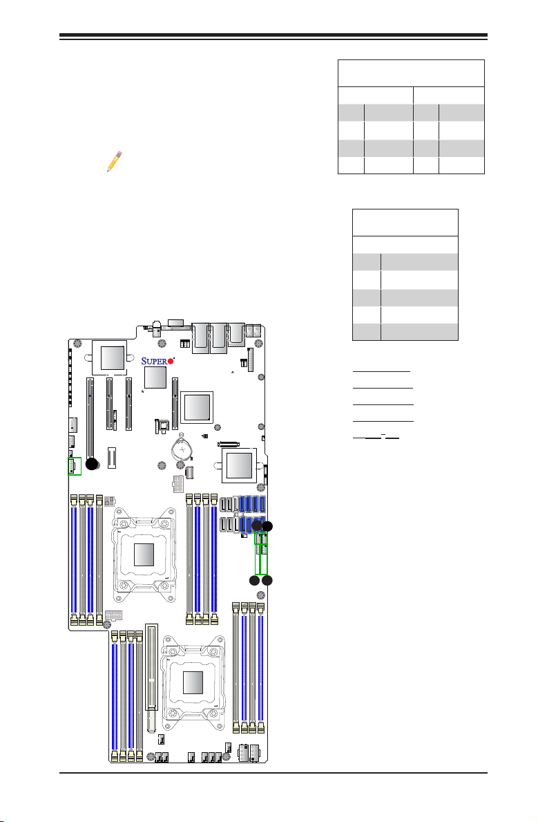
Chapter 2: Installation
E
D
T-SGPIO 1/2 & 6-SGPIO 1/2 Headers
Four SGPIO (Serial-Link General Purpose Input/
Output) headers (T-SGPIO 1/2 & 6-SGPIO 1/2)
are located on the motherboard. These headers
support onboard Serial_Link interface connections.
Note: T-SGPIO 1/2 support onboard SATA
connections. 6-SGPIO 1/2 support SAS
interface on the X9DRFF-7+/7T+.
Power SMB (I2C) Connector
Power System Management Bus (I2C) Connector
(JPI2C1) monitors power supply, fan and system
temperatures. See the table on the right for pin
denitions.
LAN2
LAN1
VGA
JPB1
JP6
JP7
X9DRFF-i(T)+_7(T)+
Rev.1.02
Intel PCH
SAS_ERR_LED2
SAS_ERR_LED1
SAS_HB_LED1
JBT1
HDD_FAULT
_LED1
BBU1
JPW1
(SATA #0-5)
IPMI_LAN
_LED1
TFM1
(SAS #0-7)
#4
#2
#3
#5
HDD_ACT
JPG1
LSI 2208
SAS CTRL
#0
#1
#4
JPS1
#5
JSD1
USB1
JTPM1
#6
#0
C
6-SGPIO2
6-SGPIO1
USB0
#3#1#7
#2
T-SGPIO2
T-SGPIO1
LSI_UART2
LSI_UART1
JPL1
JPME1
JPME2
JNMI1
CPU1 SLOT1 PCI-E 3.0 X16
JWD1
JRST1
JI2C2
JI2C1
JL1
USB2
COM1
FAN9
JPI2C1
P1 DIMMA2
P1 DIMMB1
P1 DIMMA1
FAILURE_LED1
UID_LED1
UID_SW1
Intel
LAN CTRL
JITP1
JPP1
JPP2
XDP-CPU
CLOSE 1st
Nuvotun
CPU1 SLOT3 PCI-E 3.0 X8
BMC
BMC_HB_LED1
CPLD1
CPU1
PCH SLOT2 PCI-E 2.0 X4 (IN X8)
P1 DIMMB2
JPW3
PWR_SW1
CPU2 SLOT4 PCI-E 3.0 X8
BIOS
JBAT1
T-SGPIO/6-SGPIO
PinDenitions
Pin# Denition Pin Denition
2 NC 1 NC
4 Ground 3 Data
6 Load 5 Ground
8 Clock 7 NC
Note: NC= No Connection
PWR SMB
PinDenitions
Pin# Denition
1 Clock
2 Data
3 PWR Fail
4 Ground
5 +3.3V
A. T-SGPIO1
B. T-SGPIO 2
C. 6-SGPIO 1
D. 6-SGPIO 2
2
E. JPI
C1
JPW2
P2 DIMMG1
P2 DIMMH1
P2 DIMMG2
P2 DIMMH2
OPEN 1st
P1 DIMMC2
P1 DIMMC1
P1 DIMMD2
P1 DIMMD1
SXB1_2
SXB1 CPU2 PCI-E 3.0 X16 + x16
CPU2
CLOSE 1st
SXB1_1
FAN8
FAN6
FAN5
FAN7
FAN4
P2 DIMMF1
P2 DIMME2
P2 DIMMF2
B
A
P2 DIMME1
OPEN 1st
FAN1
HDD_PWR2
FAN3
FAN2
HDD_PWR1
2-25
Page 50
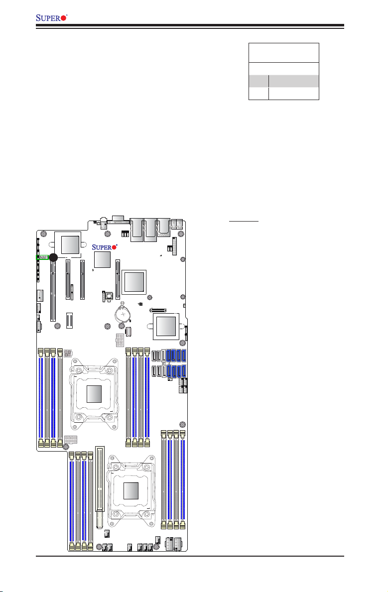
X9DRFF-i+/iT+/7+/7T+ Motherboard User’s Manual
NMI Header
The non-maskable interrupt button header is
located at JNMI1. Refer to the table on the
right for pin denitions.
LAN2
LAN1
JPB1
JP6
JP7
X9DRFF-i(T)+_7(T)+
Rev.1.02
Intel PCH
SAS_ERR_LED2
SAS_ERR_LED1
SAS_HB_LED1
JBT1
BBU1
HDD_FAULT
_LED1
TFM1
#4
#5
(SATA #0-5)
IPMI_LAN
HDD_ACT
_LED1
LSI 2208
SAS CTRL
(SAS #0-7)
#0
#2
#1
#3
JPG1
#5
#4
USB1
JPS1
#6
6-SGPIO1
JSD1
JTPM1
#0
6-SGPIO2
T-SGPIO1
JPL1
JPME1
JPME2
JNMI1
CPU1 SLOT1 PCI-E 3.0 X16
A
JWD1
JRST1
JI2C2
JI2C1
JL1
USB2
COM1
FAN9
JPI2C1
P1 DIMMA2
P1 DIMMB1
P1 DIMMA1
P1 DIMMB2
FAILURE_LED1
UID_LED1
UID_SW1
PWR_SW1
Intel
LAN CTRL
CPU1 SLOT3 PCI-E 3.0 X8
BMC_HB_LED1
JPP1
JPP2
XDP-CPU
CPU1
CLOSE 1st
Nuvotun
BMC
CPLD1
BIOS
PCH SLOT2 PCI-E 2.0 X4 (IN X8)
JITP1
JPW3
VGA
CPU2 SLOT4 PCI-E 3.0 X8
JBAT1
JPW1
USB0
#3#1#7
#2
T-SGPIO2
NMI Button
PinDenitions(JF1)
Pin# Denition
1 Control
2 Ground
A. JNMI1
LSI_UART2
LSI_UART1
JPW2
P2 DIMMG1
P2 DIMMH1
P2 DIMMG2
P2 DIMMH2
OPEN 1st
P1 DIMMC2
P1 DIMMC1
P1 DIMMD2
P1 DIMMD1
SXB1_2
SXB1 CPU2 PCI-E 3.0 X16 + x16
CPU2
CLOSE 1st
SXB1_1
FAN8
FAN6
FAN5
FAN7
P2 DIMMF1
P2 DIMME2
P2 DIMMF2
P2 DIMME1
OPEN 1st
FAN1
HDD_PWR2
FAN3
FAN2
FAN4
HDD_PWR1
2-26
Page 51
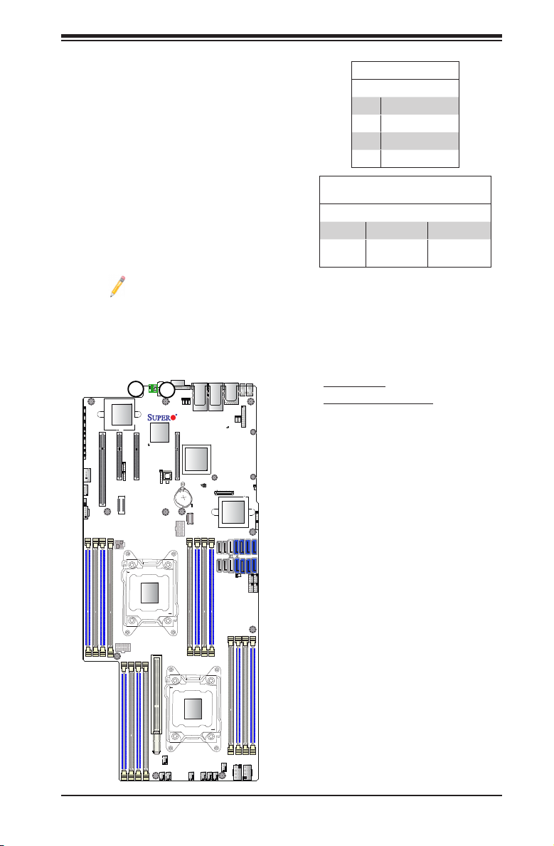
Chapter 2: Installation
COM1
HDD_PWR1
HDD_PWR2
JPW3
SXB1_1
JPW2
JPW1
FAN7
FAN6
FAN8
FAN5
FAN4
FAN3
FAN2
FAN1
UID_SW1
JPI2C1
PWR_SW1
SXB1_2
FAILURE_LED1
UID_LED1
HDD_FAULT
_LED1
USB0
T-SGPIO2
T-SGPIO1
6-SGPIO1
6-SGPIO2
JSD1
JPL1
JPME1
JPME2
JWD1
JPG1
JP7
JPB1
JP6
JPS1
Rev.1.02
X9DRFF-i(T)+_7(T)+
CPLD1
JPP1
LSI_UART2
LSI_UART1
JBT1
BMC_HB_LED1
HDD_ACT
_LED1
JL1
JNMI1
JRST1
JI2C2
JI2C1
JBAT1
JTPM1
FAN9
#4
#6
#0
#5
#3
#1
CPU2 SLOT4 PCI-E 3.0 X8
CPU1 SLOT3 PCI-E 3.0 X8
PCH SLOT2 PCI-E 2.0 X4 (IN X8)
CPU1 SLOT1 PCI-E 3.0 X16
USB2
VGA
LAN2
LAN1
IPMI_LAN
P1 DIMMA1
P1 DIMMA2
P1 DIMMB1
P1 DIMMB2
P2 DIMMG1
P2 DIMMG2
P2 DIMMH1
CPU1
P2 DIMMH2
P1 DIMMD2
P1 DIMMD1
SXB1 CPU2 PCI-E 3.0 X16 + x16
P1 DIMMC2
P1 DIMMC1
P2 DIMMF2
P2 DIMMF1
P2 DIMME2
P2 DIMME1
#2
BIOS
JPP2
CPU2
CLOSE 1st
OPEN 1st
CLOSE 1st
OPEN 1st
LSI 2208
SAS CTRL
Intel PCH
Intel
LAN CTRL
Nuvotun
BMC
(SAS #0-7)
(SATA #0-5)
SAS_ERR_LED1
SAS_ERR_LED2
SAS_HB_LED1
USB1
JITP1
XDP-CPU
BBU1
#3#1#7
#5
#0
#4
#2
TFM1
2
1
UnitIdentierSwitch
A Unit Identier switch (SW1) and a UID
LED Indicator are located on the mother-
board. The UID switch is located next to the
power switch on the backplane. The UID
LED (UID_LED1) is located next to the UID
switch. When you press the UID switch, the
UID LED Indicator will be turned on. Press
the UID switch again to turn off the UID LED.
The UID Indicator provides easy identica-
tion of a system unit that may be in need
of service.
Note: UID can also be triggered via
IPMI on the motherboard. For more
information on IPMI, please refer to
the IPMI User's Guide posted on
our website @ http://www.super-
micro.com.
UID Switch
Pin# Denition
1 Ground
2 Ground
3 Button In
4 Ground
UID LED
Status
Color/State OS Status
Blue: On Windows OS Unit Identied
Blue:
Blinking
Linux OS Unit Identied
1. UID Switch
2. UID LED (UID_LED1)
2-27
Page 52
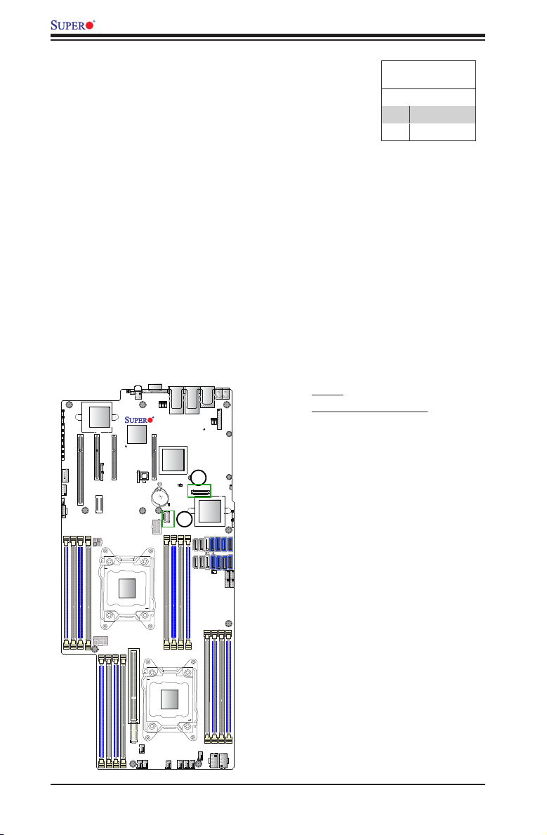
X9DRFF-i+/iT+/7+/7T+ Motherboard User’s Manual
1
2
Battery Backup Unit (BBU) Connector (X9DRF-7+/7T+
Only)
An onboard SAS battery backup unit connector is located
at BBU1 on the motherboard. This unit provides extended
battery backup support for onboard LSI 2208 SAS devices
Battery Backup Unit
PinDenitions
Pin# Denition
1 +3V Input
2 Ground
to prevent data loss during a power outage. An optional
battery backup accessory kit is required for BBU support.
Please contact our sales at Supermicro to purchase a Bat-
tery Backup Accessory kit. Also, contact our tech support for
installation instructions and possible component updates.
TFM Module Connector (X9DRF-7+/7T+ Only)
A TFM (Transportable Flash Module) connector is located at TFM1. Install a TFM
module kit (PT# BTR-0024LH-LSI00297), which contains a super capacitor, on this
connector for super cap support. A super cap is used to provide high-density power
backup support to onboard SAS storage devices to prevent data loss during a power
shortage. Refer to your server manual for Super Cap Installation instructions. See
the layout below for the location of TFM1.
LAN2
VGA
JPB1
JP6
JP7
X9DRFF-i(T)+_7(T)+
Rev.1.02
CPU2 SLOT4 PCI-E 3.0 X8
Intel PCH
SAS_ERR_LED2
SAS_HB_LED1
JBT1
JBAT1
HDD_FAULT
_LED1
BBU1
JPW1
P1 DIMMC2
P1 DIMMC1
P1 DIMMD2
P1 DIMMD1
CPU2
CLOSE 1st
LAN1
IPMI_LAN
_LED1
SAS_ERR_LED1
TFM1
LSI 2208
SAS CTRL
(SAS #0-7)
#4
#2
#3
#5
(SATA #0-5)
HDD_ACT
JPG1
JPS1
#0
#5
#1
#4
JSD1
P2 DIMMF1
P2 DIMMF2
USB1
JTPM1
#6
#0
6-SGPIO2
6-SGPIO1
P2 DIMME2
USB0
#3#1#7
#2
T-SGPIO2
T-SGPIO1
1. BBU
2. TFM Module Connector
LSI_UART2
LSI_UART1
P2 DIMME1
JPL1
JPME1
JPME2
JNMI1
CPU1 SLOT1 PCI-E 3.0 X16
JWD1
JRST1
JI2C2
JI2C1
JL1
USB2
COM1
FAN9
JPI2C1
P1 DIMMA2
P1 DIMMB1
P1 DIMMA1
FAILURE_LED1
UID_LED1
UID_SW1
Intel
LAN CTRL
Nuvotun
PCH SLOT2 PCI-E 2.0 X4 (IN X8)
CPU1 SLOT3 PCI-E 3.0 X8
BMC
BMC_HB_LED1
JPP1
CPLD1
JPP2
JITP1
XDP-CPU
P1 DIMMB2
JPW3
CPU1
CLOSE 1st
SXB1_2
P2 DIMMH2
P2 DIMMH1
P2 DIMMG2
JPW2
P2 DIMMG1
PWR_SW1
BIOS
OPEN 1st
SXB1 CPU2 PCI-E 3.0 X16 + x16
OPEN 1st
SXB1_1
FAN8
FAN6
FAN7
FAN1
HDD_PWR2
FAN3
FAN4
FAN5
HDD_PWR1
FAN2
2-28
Page 53
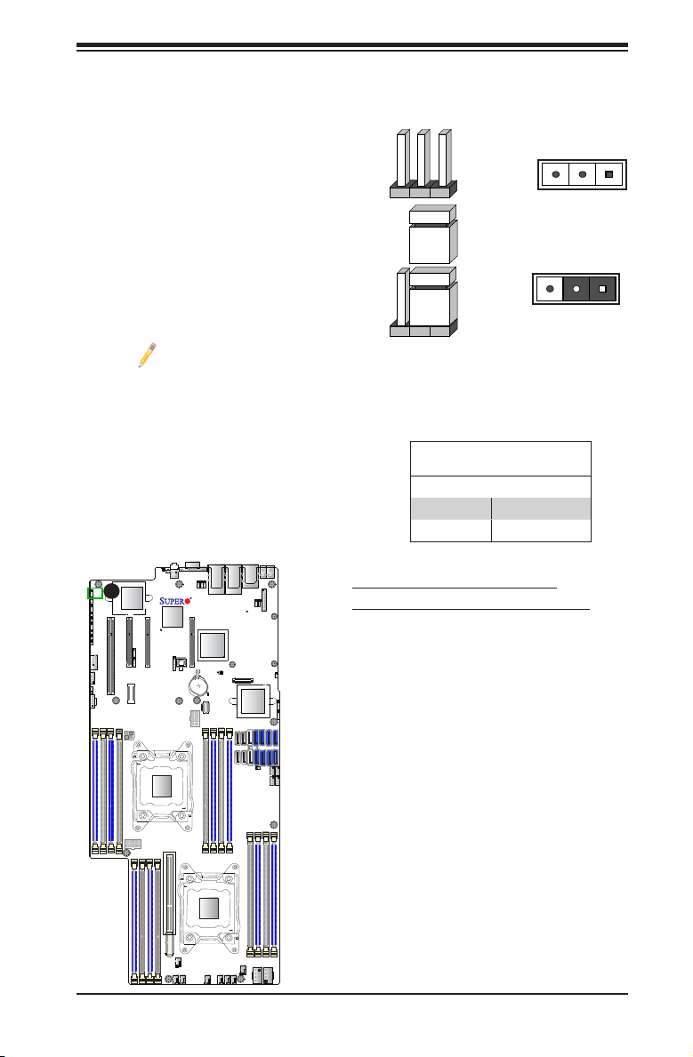
2-8 Jumper Settings
Connector
Pins
Jumper
Cap
Setting
Chapter 2: Installation
Explanation of Jumpers
To modify the operation of the mother-
board, jumpers can be used to choose
between optional settings. Jumpers create
shorts between two pins to change the
function of the connector. Pin 1 is identied
with a square solder pad on the printed
circuit board. See the motherboard layout
pages for jumper locations.
Note: On two-pin jumpers,
"Closed" means the jumper is
on and "Open" means the jumper
is off the pins.
GLAN Enable/Disable
JPL1 enables or disables LAN Port1/LAN
Port2 on the motherboard. See the table
on the right for jumper settings. The de-
fault setting is Enabled.
LAN2
VGA
JPB1
JP6
JP7
X9DRFF-i(T)+_7(T)+
Rev.1.02
CPU2 SLOT4 PCI-E 3.0 X8
Intel PCH
SAS_ERR_LED2
SAS_HB_LED1
JBT1
BIOS
JBAT1
HDD_FAULT
_LED1
BBU1
JPW1
P1 DIMMC2
P1 DIMMC1
P1 DIMMD2
P1 DIMMD1
SXB1 CPU2 PCI-E 3.0 X16 + x16
CPU2
CLOSE 1st
LAN1
IPMI_LAN
_LED1
SAS_ERR_LED1
TFM1
LSI 2208
SAS CTRL
(SAS #0-7)
#4
#2
#3
#5
(SATA #0-5)
HDD_ACT
JPG1
JPS1
#0
#5
#1
#4
JSD1
P2 DIMMF1
P2 DIMMF2
USB1
JTPM1
#6
6-SGPIO1
P2 DIMME2
#0
6-SGPIO2
T-SGPIO1
USB0
LSI_UART2
LSI_UART1
#3#1#7
#2
T-SGPIO2
P2 DIMME1
JPL1
JPME1
JPME2
JNMI1
JWD1
JRST1
JI2C2
JI2C1
JL1
USB2
COM1
FAN9
JPI2C1
P1 DIMMA2
P1 DIMMA1
Intel
A
LAN CTRL
PCH SLOT2 PCI-E 2.0 X4 (IN X8)
CPU1 SLOT1 PCI-E 3.0 X16
JPP1
JPP2
JITP1
XDP-CPU
P1 DIMMB1
P1 DIMMB2
JPW3
CLOSE 1st
P2 DIMMG2
JPW2
P2 DIMMG1
FAILURE_LED1
UID_LED1
UID_SW1
PWR_SW1
Nuvotun
CPU1 SLOT3 PCI-E 3.0 X8
BMC
BMC_HB_LED1
CPLD1
CPU1
OPEN 1st
SXB1_2
P2 DIMMH2
P2 DIMMH1
3 2 1
3 2 1
Pin 1-2 short
LAN Enable
Jumper Settings
Jumper Setting Denition
1-2 Enabled (default)
2-3 Disabled
A. GLAN1/2 Enable (X9DRFF-i+/7+)
A. 10G LAN1/2 Enable (X9DRFF-iT+/7T+)
SXB1_1
OPEN 1st
FAN8
FAN6
FAN7
FAN1
HDD_PWR2
HDD_PWR1
FAN3
FAN2
FAN4
FAN5
2-29
Page 54
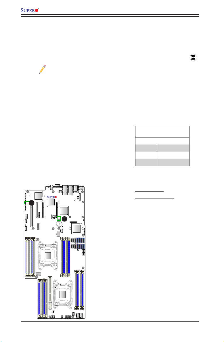
X9DRFF-i+/iT+/7+/7T+ Motherboard User’s Manual
CMOS Clear
JBT1 is used to clear CMOS. Instead of pins, this "jumper" consists of contact pads
to prevent accidental clearing of CMOS. To clear CMOS, use a metal object such
as a small screwdriver to touch both pads at the same time to short the connection.
Always remove the AC power cord from the system before clearing CMOS.
Note 1: For an ATX power supply, you must completely shut down the
system, remove the AC power cord, and then short JBT1 to clear CMOS.
Note 2: Be sure to remove the onboard CMOS Battery before you short
JBT1 to clear CMOS.
Note 3: Clearing CMOS will also clear all passwords.
Watch Dog Enable/Disable
Watch Dog (JWD1) is a system monitor that
will reboot the system when a software ap-
plication hangs. Close pins 1-2 to reset the
system if an application hangs. Close pins
2-3 to generate a non-maskable interrupt
signal for the application that hangs. See the
Watch Dog
Jumper Settings
Jumper Setting Denition
Pins 1-2 Reset (default)
Pins 2-3 NMI
Open Disabled
table on the right for jumper settings. Watch
Dog must also be enabled in the BIOS.
LAN2
VGA
JPB1
JP6
JP7
X9DRFF-i(T)+_7(T)+
Rev.1.02
CPU2 SLOT4 PCI-E 3.0 X8
Intel PCH
SAS_ERR_LED2
SAS_HB_LED1
JBT1
BIOS
A
JBAT1
HDD_FAULT
_LED1
BBU1
JPW1
P1 DIMMC2
P1 DIMMC1
P1 DIMMD2
P1 DIMMD1
SXB1 CPU2 PCI-E 3.0 X16 + x16
CPU2
CLOSE 1st
LAN1
IPMI_LAN
_LED1
SAS_ERR_LED1
TFM1
LSI 2208
SAS CTRL
(SAS #0-7)
#4
#2
#3
#5
(SATA #0-5)
HDD_ACT
JPG1
#0
#5
#1
#4
P2 DIMMF2
USB1
JPS1
JTPM1
#6
6-SGPIO1
JSD1
P2 DIMMF1
#2
#0
6-SGPIO2
T-SGPIO1
P2 DIMME2
USB0
#3#1#7
A. Clear CMOS
B. Watch Dog Enable
LSI_UART2
LSI_UART1
T-SGPIO2
P2 DIMME1
JPL1
JPME1
JPME2
JNMI1
JWD1
JRST1
JI2C2
JI2C1
JL1
USB2
COM1
FAN9
JPI2C1
P1 DIMMA1
B
P1 DIMMA2
P1 DIMMB1
CPU1 SLOT1 PCI-E 3.0 X16
FAILURE_LED1
UID_LED1
Intel
LAN CTRL
PCH SLOT2 PCI-E 2.0 X4 (IN X8)
CPU1 SLOT3 PCI-E 3.0 X8
BMC_HB_LED1
JPP1
JPP2
JITP1
XDP-CPU
P1 DIMMB2
JPW3
CPU1
CLOSE 1st
P2 DIMMH2
P2 DIMMH1
P2 DIMMG2
JPW2
P2 DIMMG1
UID_SW1
PWR_SW1
Nuvotun
BMC
CPLD1
OPEN 1st
SXB1_2
SXB1_1
OPEN 1st
FAN8
FAN7
FAN1
HDD_PWR2
HDD_PWR1
FAN3
FAN2
FAN4
FAN6
FAN5
2-30
Page 55
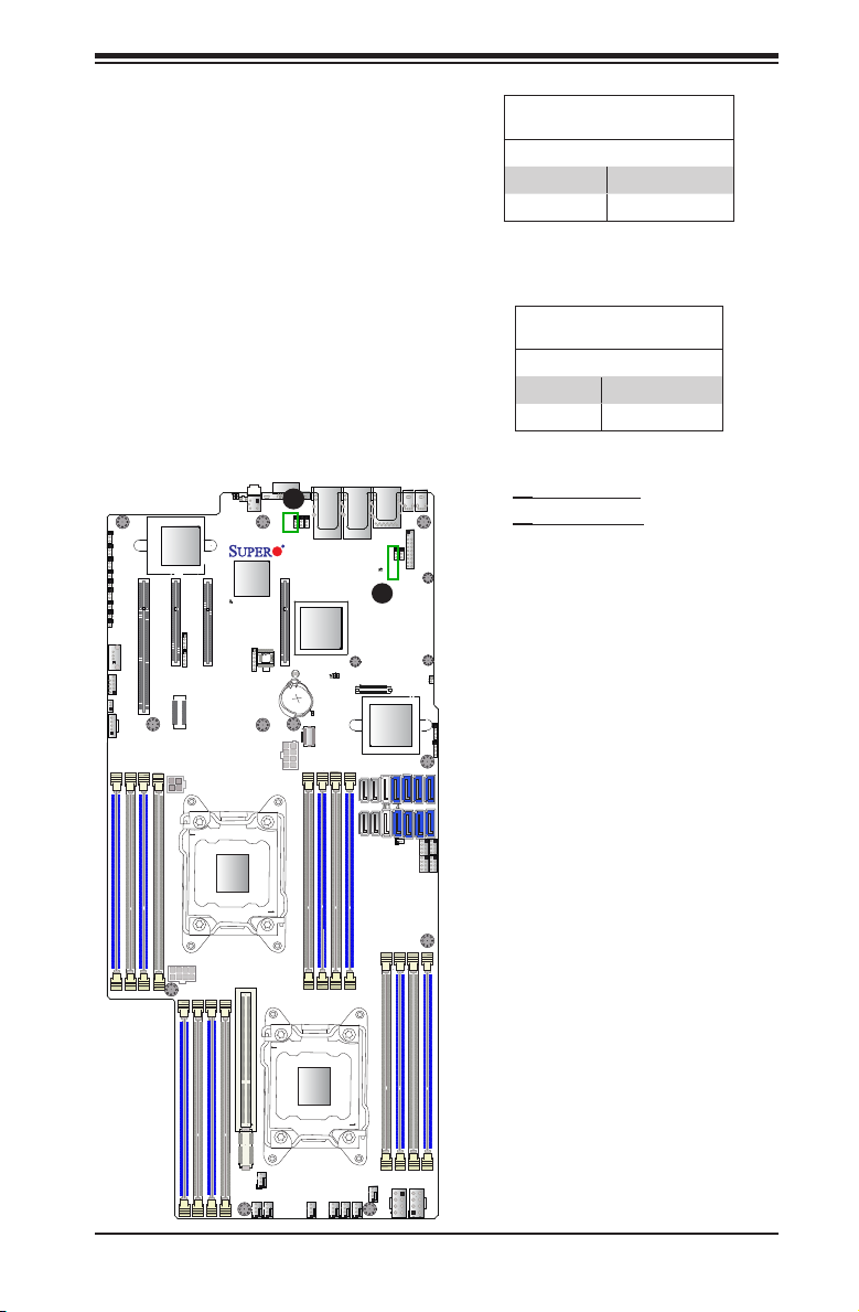
Chapter 2: Installation
VGA Enable
Jumper JPG1 allows the user to en-
able onboard VGA support. The default
setting is on pins 1-2 to enable VGA
support. See the table on the right for
jumper settings.
BMC Enable
Jumper JPB1 allows you to enable the
embedded BMC (Baseboard Manage-
ment) Controller to provide IPMI 2.0 sup-
port on the motherboard. See the table
on the right for jumper settings.
LAN2
LAN1
B
JPB1
JP6
JP7
X9DRFF-i(T)+_7(T)+
Rev.1.02
Intel PCH
SAS_ERR_LED2
SAS_ERR_LED1
SAS_HB_LED1
JBT1
BBU1
HDD_FAULT
_LED1
TFM1
(SAS #0-7)
#4
#5
(SATA #0-5)
IPMI_LAN
HDD_ACT
_LED1
JPG1
A
LSI 2208
SAS CTRL
#0
#2
#1
#4
#3
JPS1
#5
JSD1
JPL1
JPME1
JPME2
JNMI1
CPU1 SLOT1 PCI-E 3.0 X16
JWD1
JRST1
JI2C2
JI2C1
JL1
USB2
COM1
FAN9
JPI2C1
P1 DIMMA2
P1 DIMMB1
P1 DIMMA1
FAILURE_LED1
UID_LED1
UID_SW1
Intel
LAN CTRL
CPU1 SLOT3 PCI-E 3.0 X8
BMC_HB_LED1
JPP1
JPP2
XDP-CPU
CPU1
CLOSE 1st
Nuvotun
BMC
CPLD1
PCH SLOT2 PCI-E 2.0 X4 (IN X8)
JITP1
P1 DIMMB2
JPW3
VGA
PWR_SW1
CPU2 SLOT4 PCI-E 3.0 X8
BIOS
JBAT1
JPW1
USB1
JTPM1
#6
#0
6-SGPIO2
6-SGPIO1
USB0
#3#1#7
#2
T-SGPIO2
T-SGPIO1
VGA Enable
Jumper Settings
Jumper Setting Denition
1-2 Enabled (Default)
2-3 Disabled
BMC Enable
Jumper Settings
Jumper Setting Denition
Pins 1-2 BMC Enable
Pins 2-3 Normal (Default)
A. VGA Enabled
B. BMC Enabled
LSI_UART2
LSI_UART1
JPW2
P2 DIMMG1
P2 DIMMH1
P2 DIMMG2
P2 DIMMH2
OPEN 1st
P1 DIMMC2
P1 DIMMC1
P1 DIMMD2
P1 DIMMD1
SXB1_2
SXB1 CPU2 PCI-E 3.0 X16 + x16
CPU2
CLOSE 1st
SXB1_1
FAN8
FAN6
FAN5
FAN7
P2 DIMMF1
P2 DIMME2
P2 DIMMF2
P2 DIMME1
OPEN 1st
FAN1
HDD_PWR2
FAN3
FAN2
FAN4
HDD_PWR1
2-31
Page 56
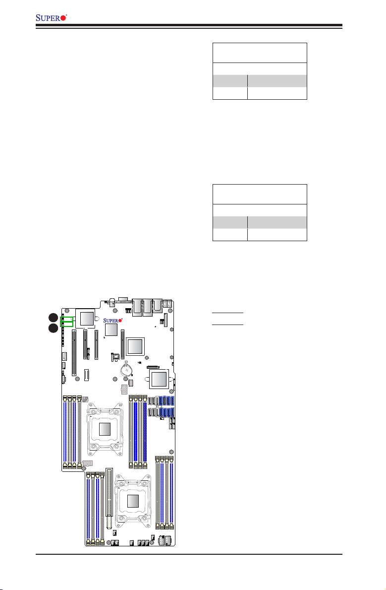
X9DRFF-i+/iT+/7+/7T+ Motherboard User’s Manual
COM1
HDD_PWR1
HDD_PWR2
JPW3
SXB1_1
JPW2
JPW1
FAN7
FAN6
FAN8
FAN5
FAN4
FAN3
FAN2
FAN1
UID_SW1
JPI2C1
PWR_SW1
SXB1_2
FAILURE_LED1
UID_LED1
HDD_FAULT
_LED1
USB0
T-SGPIO2
T-SGPIO1
6-SGPIO1
6-SGPIO2
JSD1
JPL1
JPME1
JPME2
JWD1
JPG1
JP7
JPB1
JP6
JPS1
Rev.1.02
X9DRFF-i(T)+_7(T)+
CPLD1
JPP1
LSI_UART2
LSI_UART1
JBT1
BMC_HB_LED1
HDD_ACT
_LED1
JL1
JNMI1
JRST1
JI2C2
JI2C1
JBAT1
JTPM1
FAN9
#4
#6
#0
#5
#3
#1
CPU2 SLOT4 PCI-E 3.0 X8
CPU1 SLOT3 PCI-E 3.0 X8
PCH SLOT2 PCI-E 2.0 X4 (IN X8)
CPU1 SLOT1 PCI-E 3.0 X16
USB2
VGA
LAN2
LAN1
IPMI_LAN
P1 DIMMA1
P1 DIMMA2
P1 DIMMB1
P1 DIMMB2
P2 DIMMG1
P2 DIMMG2
P2 DIMMH1
CPU1
P2 DIMMH2
P1 DIMMD2
P1 DIMMD1
SXB1 CPU2 PCI-E 3.0 X16 + x16
P1 DIMMC2
P1 DIMMC1
P2 DIMMF2
P2 DIMMF1
P2 DIMME2
P2 DIMME1
#2
BIOS
JPP2
CPU2
CLOSE 1st
OPEN 1st
CLOSE 1st
OPEN 1st
LSI 2208
SAS CTRL
Intel PCH
Intel
LAN CTRL
Nuvotun
BMC
(SAS #0-7)
(SATA #0-5)
SAS_ERR_LED1
SAS_ERR_LED2
SAS_HB_LED1
USB1
JITP1
XDP-CPU
BBU1
#3#1#7
#5
#0
#4
#2
TFM1
Management Engine (ME) Recovery
Use Jumper JPME1 to select ME Firm-
ware Recovery mode, which will limit
resource allocation for essential system
operation only in order to maintain nor-
mal power operation and management.
In the single operation mode, online
upgrade will be available via Recovery
mode. See the table on the right for
jumper settings.
Manufacture Mode Select
Close Pin 2 and Pin 3 of Jumper JPME2
to bypass SPI ash security and force
the system to operate in the Manufac-
ture Mode, allowing the user to ash the
system rmware from a host server for
system setting modications. See the
table on the right for jumper settings.
A
B
ME Recovery
Jumper Settings
Jumper Setting Denition
1-2 Normal (Default)
2-3 ME Recovery
ME Mode Select
Jumper Settings
Jumper Setting Denition
1-2 Normal (Default)
2-3 Manufacture Mode
A. JPME1
B. JPME2
2-32
Page 57
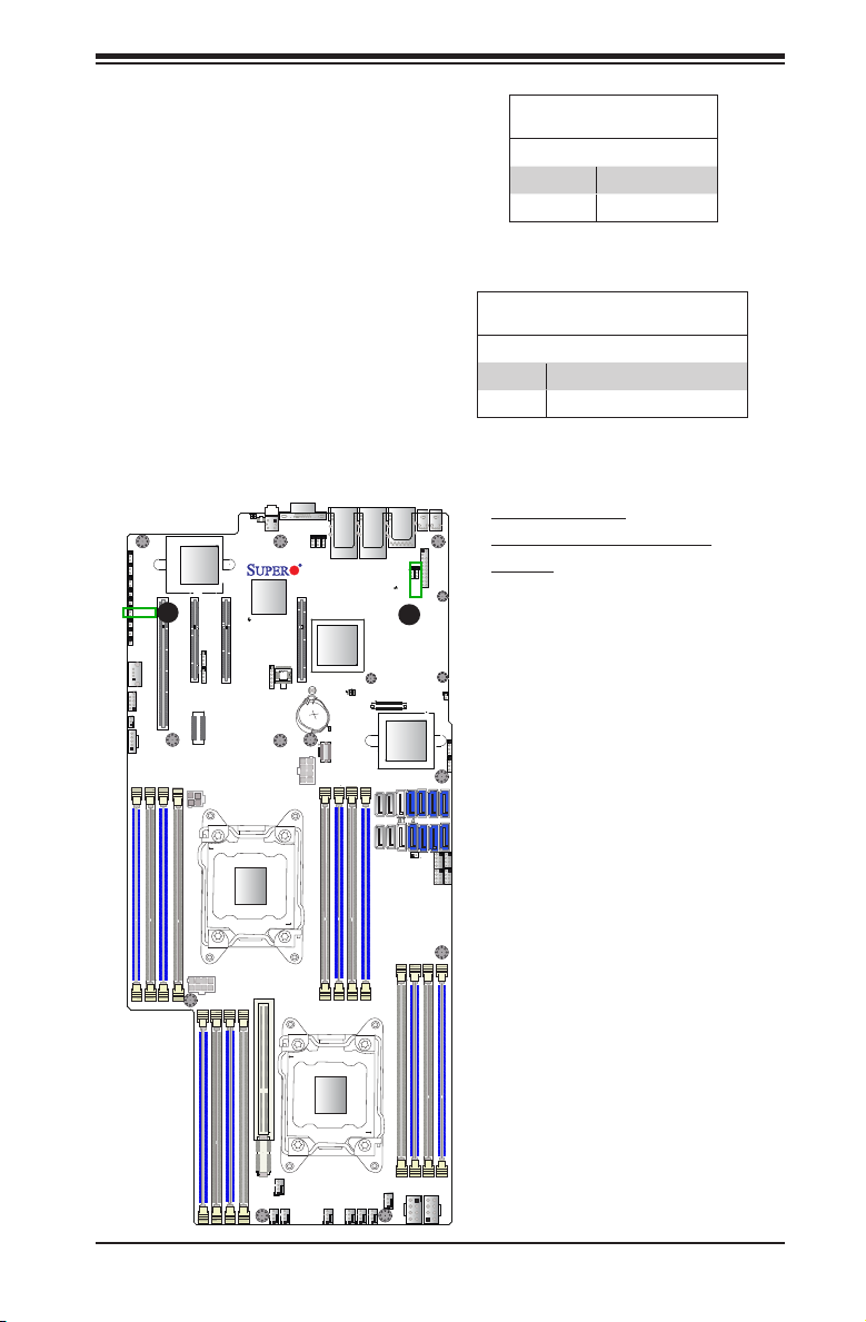
Chapter 2: Installation
LSI_UART2
LSI_UART1
P2 DIMME1
System Reset
Close the pins of JRST1 to reset BMC
settings. See the table on the right for
jumper settings.
SAS Enable (For X9DRFF-7+/7T+)
Use Jumper JPS1 to enable onboard
SAS support to enhance system perfor-
mance. The default setting is enabled.
LAN2
LAN1
JPB1
JP6
JP7
X9DRFF-i(T)+_7(T)+
Rev.1.02
Intel PCH
SAS_ERR_LED2
SAS_ERR_LED1
SAS_HB_LED1
JBT1
HDD_FAULT
_LED1
BBU1
JPW1
(SATA #0-5)
IPMI_LAN
TFM1
(SAS #0-7)
#4
#3
#5
HDD_ACT
_LED1
JPG1
B
LSI 2208
SAS CTRL
#0
#2
#1
#5
#4
USB1
JPS1
#6
6-SGPIO1
JSD1
JTPM1
#0
6-SGPIO2
T-SGPIO1
JPL1
JPME1
JPME2
JNMI1
CPU1 SLOT1 PCI-E 3.0 X16
JWD1
JRST1
A
JI2C2
JI2C1
JL1
USB2
COM1
FAN9
JPI2C1
P1 DIMMA2
P1 DIMMB1
P1 DIMMA1
FAILURE_LED1
UID_LED1
UID_SW1
Intel
LAN CTRL
CPU1 SLOT3 PCI-E 3.0 X8
BMC_HB_LED1
JPP1
JPP2
XDP-CPU
CPU1
CLOSE 1st
Nuvotun
BMC
CPLD1
PCH SLOT2 PCI-E 2.0 X4 (IN X8)
JITP1
P1 DIMMB2
JPW3
VGA
PWR_SW1
CPU2 SLOT4 PCI-E 3.0 X8
BIOS
JBAT1
System Reset
Jumper Settings
Jumper Setting Denition
Pins 1-2 BMC Reset
Pins 2-3 Normal (Default)
SAS Support Enable
Jumper Settings
Jumper Setting Denition
Pins 1/2 SAS Enabled (Default)
Pins 2/3 SAS Disabled
USB0
A. System Reset
B. SAS Enable (X9DRFF-
7+/7T+)
#3#1#7
#2
T-SGPIO2
JPW2
P2 DIMMG1
P2 DIMMH1
P2 DIMMG2
P2 DIMMH2
OPEN 1st
P1 DIMMC2
P1 DIMMC1
P1 DIMMD2
P1 DIMMD1
SXB1_2
SXB1 CPU2 PCI-E 3.0 X16 + x16
CPU2
CLOSE 1st
SXB1_1
FAN8
FAN6
FAN5
FAN7
OPEN 1st
FAN4
P2 DIMMF1
P2 DIMME2
P2 DIMMF2
FAN1
HDD_PWR2
FAN3
FAN2
HDD_PWR1
2-33
Page 58
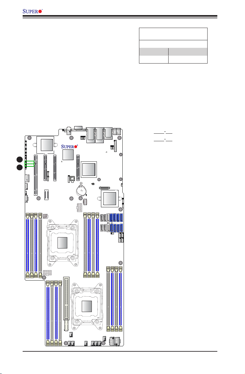
X9DRFF-i+/iT+/7+/7T+ Motherboard User’s Manual
I2C Bus to PCI-Exp. Slots
Jumpers JI2C1 and JI2C2 allow you to con-
nect the System Management Bus (I2C) to
PCI-Express slots. The default setting is
Open to disable the connection.
FAILURE_LED1
UID_LED1
UID_SW1
PWR_SW1
Intel
JPL1
LAN CTRL
JPME1
JPME2
PCH SLOT2 PCI-E 2.0 X4 (IN X8)
JNMI1
CPU1 SLOT1 PCI-E 3.0 X16
JWD1
JRST1
B
JI2C2
JI2C1
A
JL1
USB2
COM1
JITP1
FAN9
JPI2C1
P1 DIMMA2
P1 DIMMB1
P1 DIMMA1
P1 DIMMB2
JPW3
CPU1 SLOT3 PCI-E 3.0 X8
BMC_HB_LED1
JPP1
JPP2
XDP-CPU
CPU1
CLOSE 1st
Nuvotun
BMC
CPLD1
LAN2
VGA
JPB1
JP6
JP7
X9DRFF-i(T)+_7(T)+
Rev.1.02
CPU2 SLOT4 PCI-E 3.0 X8
Intel PCH
JBT1
BIOS
JBAT1
HDD_FAULT
_LED1
BBU1
JPW1
SAS_ERR_LED2
SAS_HB_LED1
LAN1
IPMI_LAN
HDD_ACT
_LED1
SAS_ERR_LED1
TFM1
LSI 2208
SAS CTRL
(SAS #0-7)
#0
#4
#2
#1
#3
#5
(SATA #0-5)
JPG1
#5
#4
JSD1
USB1
JPS1
JTPM1
#6
6-SGPIO1
USB0
#3#1#7
#2
#0
6-SGPIO2
T-SGPIO2
T-SGPIO1
Jumper Settings
Jumper Setting Denition
Closed Enabled
Open Disabled (Default)
A. JI2C1
B. JI2C2
LSI_UART2
LSI_UART1
I2C to PCI-Exp
JPW2
P2 DIMMG1
P2 DIMMH1
P2 DIMMG2
P2 DIMMH2
OPEN 1st
P1 DIMMC2
P1 DIMMC1
P1 DIMMD2
P1 DIMMD1
SXB1_2
SXB1 CPU2 PCI-E 3.0 X16 + x16
CPU2
CLOSE 1st
SXB1_1
FAN8
FAN6
FAN5
FAN7
P2 DIMMF1
P2 DIMME2
P2 DIMMF2
P2 DIMME1
OPEN 1st
FAN1
HDD_PWR2
FAN3
FAN2
FAN4
HDD_PWR1
2-34
Page 59
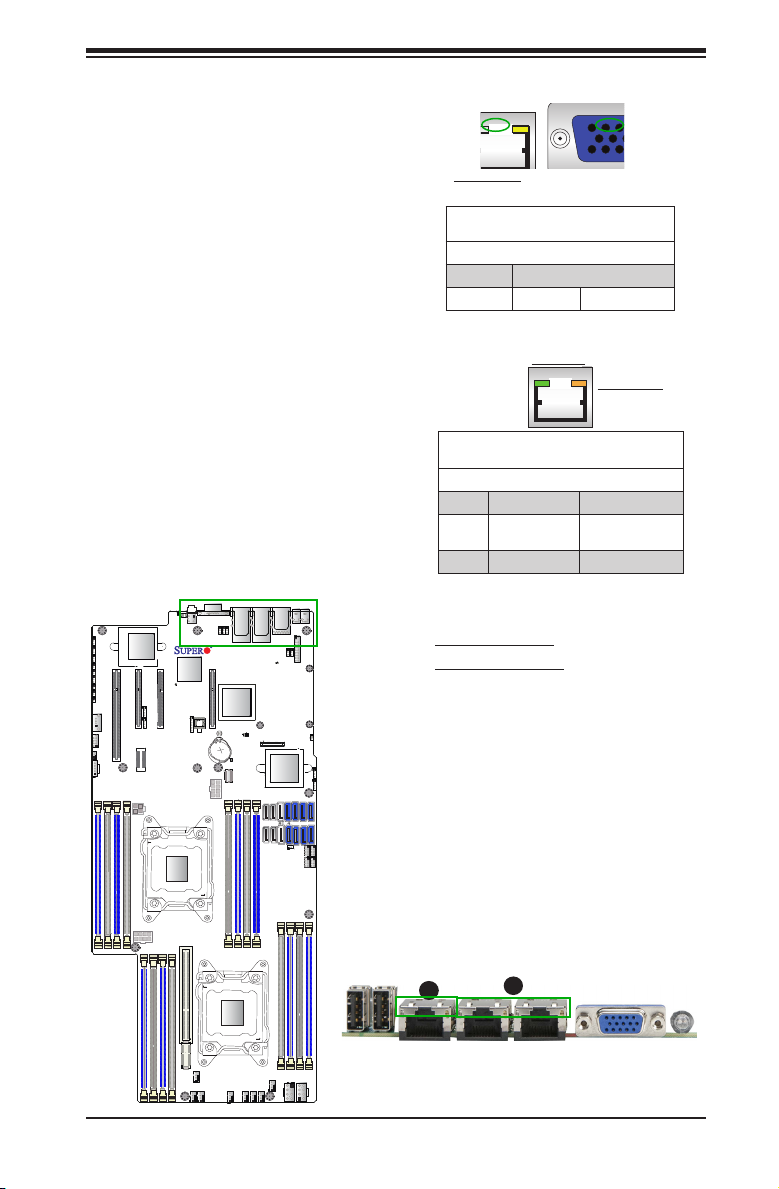
2-9 Onboard LED Indicators
GLAN LEDs
There are two LAN ports (LAN1/2) on the
motherboard. Each Ethernet LAN port has
two LEDs. The Yellow LED on the right
indicates connection and activity. The
Link LED on the left side may be green,
amber or off to indicate the speed of the
connection. See the table on the right for
more information.
IPMI Dedicated LAN LEDs
In addition to LAN Ports 1/2, an IPMI
Dedicated LAN is also located on the I/O
Backplane. The amber LED on the right
indicates connection and activity; while
the green LED on the left indicates the
speed of the connection. See the table
on the right for more information.
LAN2
VGA
JPB1
JP6
JP7
X9DRFF-i(T)+_7(T)+
Rev.1.02
CPU2 SLOT4 PCI-E 3.0 X8
Intel PCH
JBT1
BIOS
JBAT1
BBU1
JPW1
P1 DIMMC2
P1 DIMMC1
P1 DIMMD2
P1 DIMMD1
CPU2
CLOSE 1st
SAS_HB_LED1
HDD_FAULT
_LED1
LAN1
IPMI_LAN
_LED1
SAS_ERR_LED2
SAS_ERR_LED1
TFM1
(SAS #0-7)
#4
#2
#3
#5
(SATA #0-5)
HDD_ACT
LSI 2208
SAS CTRL
#0
#1
P2 DIMMF2
JPG1
JPS1
#5
#4
JSD1
P2 DIMMF1
USB1
JTPM1
#6
6-SGPIO1
USB0
#3#1#7
#2
#0
6-SGPIO2
T-SGPIO1
P2 DIMME2
LSI_UART2
LSI_UART1
T-SGPIO2
P2 DIMME1
JPL1
JPME1
JPME2
JNMI1
JWD1
JRST1
JI2C2
JI2C1
JL1
USB2
COM1
FAN9
JPI2C1
P1 DIMMA1
P1 DIMMA2
P1 DIMMB1
CPU1 SLOT1 PCI-E 3.0 X16
FAILURE_LED1
UID_LED1
UID_SW1
Intel
LAN CTRL
Nuvotun
PCH SLOT2 PCI-E 2.0 X4 (IN X8)
CPU1 SLOT3 PCI-E 3.0 X8
BMC
BMC_HB_LED1
JPP1
JPP2
JITP1
XDP-CPU
P1 DIMMB2
JPW3
CPU1
CLOSE 1st
P2 DIMMH2
P2 DIMMH1
P2 DIMMG2
JPW2
P2 DIMMG1
PWR_SW1
CPLD1
OPEN 1st
SXB1_2
SXB1 CPU2 PCI-E 3.0 X16 + x16
Chapter 2: Installation
Link Speed LED
Rear View (when facing the
rear side of the chassis)
GLAN/TLAN Activity Indicator (Right)
Color Status Denition
Off No Connections
Yellow Flashing Active
Link Speed LED
IPMI LAN Link Speed LED (Left) &
LED Color/State Denition
Off Off No Connection
Activity Amber:
Speed Green: Solid 100 Mbps
LED Settings
IPMI LAN
Connection Activity LED (Right)
Blinking
A. LAN1/2 LEDs
B. IPMI LAN LEDs
B
A
Activity LED
Activity LED
Active
SXB1_1
OPEN 1st
FAN8
FAN6
FAN7
FAN1
HDD_PWR2
FAN3
FAN4
FAN5
HDD_PWR1
FAN2
2-35
Page 60
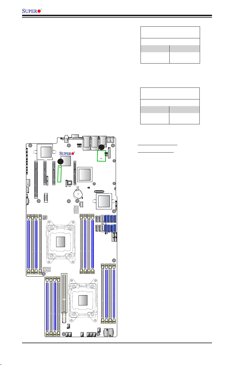
X9DRFF-i+/iT+/7+/7T+ Motherboard User’s Manual
HDD Activity LED
An HDD Activity LED is located at
HDD_ ACT LED1 on the motherboard.
When the HDD LED is blinking, an HDD
device is active. See the table on the right
for more information.
BMC Heartbeat LED
A BMC Hear tbeat LED is located at
BMC_HB_ LED1 on the motherboard.
When this LED indicator is blinking, BMC
is normal. See the table on the right for
more information.
LAN2
LAN1
JPB1
JP6
JP7
X9DRFF-i(T)+_7(T)+
Rev.1.02
Intel PCH
SAS_ERR_LED2
SAS_ERR_LED1
SAS_HB_LED1
JBT1
HDD_FAULT
_LED1
BBU1
TFM1
#4
#5
(SATA #0-5)
A
IPMI_LAN
HDD_ACT
_LED1
LSI 2208
SAS CTRL
(SAS #0-7)
#0
#2
#1
#3
JPG1
#4
JPS1
#5
JSD1
USB1
JTPM1
#6
#0
6-SGPIO2
6-SGPIO1
T-SGPIO1
JPL1
JPME1
JPME2
JNMI1
CPU1 SLOT1 PCI-E 3.0 X16
JWD1
JRST1
JI2C2
JI2C1
JL1
USB2
COM1
FAN9
JPI2C1
P1 DIMMA2
P1 DIMMB1
P1 DIMMA1
P1 DIMMB2
FAILURE_LED1
UID_LED1
UID_SW1
PWR_SW1
Intel
LAN CTRL
JITP1
JPP1
JPP2
XDP-CPU
CLOSE 1st
Nuvotun
CPU1 SLOT3 PCI-E 3.0 X8
B
BMC
BMC_HB_LED1
CPLD1
CPU1
PCH SLOT2 PCI-E 2.0 X4 (IN X8)
JPW3
VGA
CPU2 SLOT4 PCI-E 3.0 X8
BIOS
JBAT1
JPW1
USB0
LSI_UART2
LSI_UART1
#3#1#7
#2
T-SGPIO2
HDD Activity LED
Status
Color or State Denition
Green: Blinking HDD: Active
Off HDD Disabled,
BMC Heartbeat LED
or Failed
Status
Color or State Denition
Green BMC: Normal
Off or Red BMC Disabled,
or Failed
A. HDD_ACT LED1
B. BMC_HB LED1
JPW2
P2 DIMMG1
P2 DIMMH1
P2 DIMMG2
P2 DIMMH2
OPEN 1st
P1 DIMMC2
P1 DIMMC1
P1 DIMMD2
P1 DIMMD1
SXB1_2
SXB1 CPU2 PCI-E 3.0 X16 + x16
CPU2
CLOSE 1st
SXB1_1
FAN8
FAN6
FAN5
FAN7
P2 DIMMF1
P2 DIMME2
P2 DIMMF2
P2 DIMME1
OPEN 1st
FAN1
HDD_PWR2
FAN3
FAN2
FAN4
HDD_PWR1
2-36
Page 61
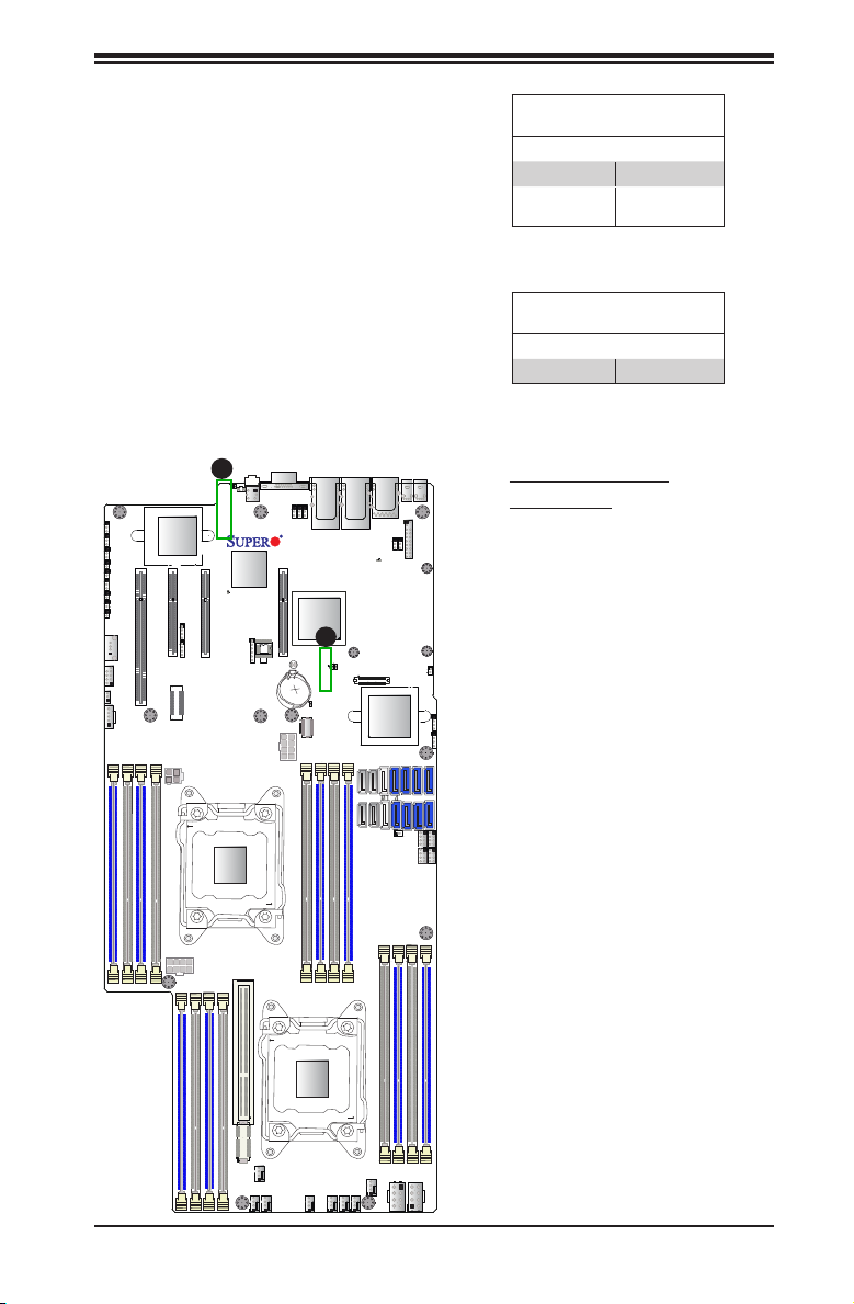
Chapter 2: Installation
SAS Heartbeat LED
A SAS Heartbeat LED is located at
SAS_HB_LED1 on the motherboard.
When LEDS2 is blinking, SAS is working
properly.
BMC Failure LED
A BMC Failure LED is located at Fail-
ure_LED1 on the motherboard. When
this LED indicator is on, BMC is not work-
ing properly. See the table on the right for
more information.
JPL1
JPME1
JPME2
JNMI1
CPU1 SLOT1 PCI-E 3.0 X16
JWD1
JRST1
JI2C2
JI2C1
JL1
USB2
COM1
FAN9
JPI2C1
P1 DIMMA2
P1 DIMMB1
P1 DIMMA1
B
FAILURE_LED1
UID_LED1
UID_SW1
Intel
LAN CTRL
CPU1 SLOT3 PCI-E 3.0 X8
BMC_HB_LED1
JPP1
JPP2
XDP-CPU
CPU1
CLOSE 1st
Nuvotun
BMC
CPLD1
PCH SLOT2 PCI-E 2.0 X4 (IN X8)
JITP1
P1 DIMMB2
JPW3
PWR_SW1
LAN2
VGA
JPB1
JP6
JP7
X9DRFF-i(T)+_7(T)+
Rev.1.02
CPU2 SLOT4 PCI-E 3.0 X8
Intel PCH
JBT1
BIOS
JBAT1
HDD_FAULT
_LED1
BBU1
JPW1
LAN1
A
SAS_ERR_LED2
SAS_ERR_LED1
SAS_HB_LED1
(SATA #0-5)
TFM1
(SAS #0-7)
#4
#5
IPMI_LAN
HDD_ACT
_LED1
LSI 2208
SAS CTRL
#0
#2
#1
#3
JPG1
#5
#4
USB1
JPS1
#6
6-SGPIO1
JSD1
JTPM1
#0
6-SGPIO2
T-SGPIO1
USB0
#3#1#7
#2
T-SGPIO2
SAS Heartbeat LED
Status
Color/State Denition
Green: Blinking SAS: Normal
Off or Red SAS: Disabled or
Failed
BMC Failure LED
Status
State Denition
On BMC: Failed
A. SAS Heartbeat LED
B. Failure LED
LSI_UART2
LSI_UART1
JPW2
P2 DIMMG1
P2 DIMMH1
P2 DIMMG2
P2 DIMMH2
OPEN 1st
P1 DIMMC2
P1 DIMMC1
P1 DIMMD2
P1 DIMMD1
SXB1_2
SXB1 CPU2 PCI-E 3.0 X16 + x16
CPU2
CLOSE 1st
SXB1_1
FAN8
FAN6
FAN5
FAN7
P2 DIMMF1
P2 DIMME2
P2 DIMMF2
P2 DIMME1
OPEN 1st
FAN1
HDD_PWR2
FAN3
FAN2
FAN4
HDD_PWR1
2-37
Page 62
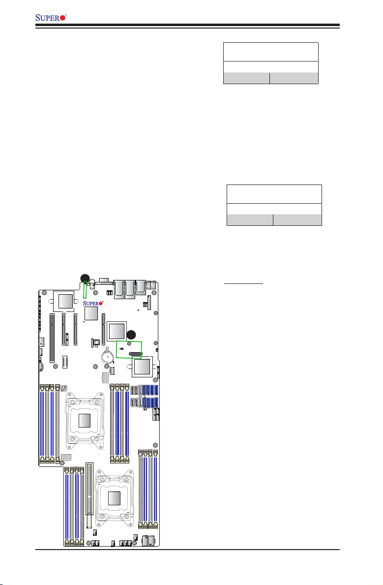
X9DRFF-i+/iT+/7+/7T+ Motherboard User’s Manual
UID LED
The Unit Identier (UID) LED is located at
UID_LED1 on the motherboard. When this
LED is on, the unit that might be in need of
service is identied. See the table on the right
for more information.
SAS Error LEDs
SAS Error LEDs are located at SAS_Err_
LED1/2 on the motherboard. When SASLED
indicator is on, BMC is not working properly.
See the table on the right for more information.
LAN2
VGA
JPB1
JP6
JP7
X9DRFF-i(T)+_7(T)+
Rev.1.02
CPU2 SLOT4 PCI-E 3.0 X8
Intel PCH
SAS_ERR_LED2
SAS_HB_LED1
JBT1
JBAT1
HDD_FAULT
_LED1
BBU1
JPW1
P1 DIMMC2
P1 DIMMC1
P1 DIMMD2
P1 DIMMD1
CPU2
CLOSE 1st
LAN1
IPMI_LAN
_LED1
B
SAS_ERR_LED1
TFM1
LSI 2208
SAS CTRL
(SAS #0-7)
#4
#2
#3
#5
(SATA #0-5)
HDD_ACT
JPG1
JPS1
#0
#5
#1
#4
JSD1
P2 DIMMF1
P2 DIMMF2
USB1
JTPM1
#6
#0
6-SGPIO2
6-SGPIO1
P2 DIMME2
USB0
#3#1#7
#2
T-SGPIO1
LSI_UART2
LSI_UART1
T-SGPIO2
P2 DIMME1
JPL1
JPME1
JPME2
JNMI1
JWD1
JRST1
JI2C2
JI2C1
JL1
USB2
COM1
FAN9
JPI2C1
P1 DIMMA1
P1 DIMMA2
P1 DIMMB1
CPU1 SLOT1 PCI-E 3.0 X16
A
FAILURE_LED1
UID_LED1
UID_SW1
Intel
LAN CTRL
Nuvotun
PCH SLOT2 PCI-E 2.0 X4 (IN X8)
CPU1 SLOT3 PCI-E 3.0 X8
BMC
BMC_HB_LED1
JPP1
JPP2
JITP1
XDP-CPU
P1 DIMMB2
JPW3
CPU1
CLOSE 1st
P2 DIMMH2
P2 DIMMH1
P2 DIMMG2
JPW2
P2 DIMMG1
PWR_SW1
CPLD1
BIOS
OPEN 1st
SXB1_2
SXB1 CPU2 PCI-E 3.0 X16 + x16
Rear UID LED
Status
Color/State Denition
Blue: On Unit Identied
SAS_ERR_LED1/2 Failure LED
Status
State Denition
On SAS: Failed
A. UID LED
B. SAS_ Err_LED1/2
SXB1_1
OPEN 1st
FAN8
FAN6
FAN7
FAN1
HDD_PWR2
FAN3
FAN4
FAN5
HDD_PWR1
FAN2
2-38
Page 63
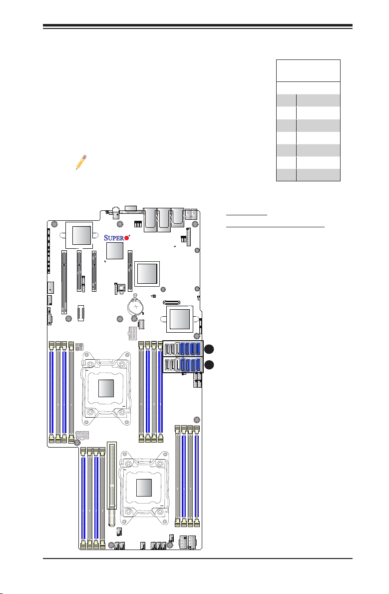
2-10 SATA/SAS Connections
Chapter 2: Installation
SATA/SAS Ports
Eight Serial_ATA ports are located on the motherboard.
I-SATA Ports 0/1 support SATA 3.0. I-SATA Ports 2-5 and
S-SATA 0 support SATA 2.0. In addition, eight SAS ports
(L-SAS 0-7), supported by the LSI SAS 2208 Controller
are also located on the X9DRFF-7+/7T+. See the table on
the right for pin denitions.
Note: For more information on SATA HostRAID
conguration, please refer to the Intel SATA and
LSI SAS HostRAID User's Guides posted on our
website @ http://www.supermicro.com..
LAN2
LAN1
JPB1
JP6
JP7
X9DRFF-i(T)+_7(T)+
Rev.1.02
Intel PCH
SAS_ERR_LED2
SAS_ERR_LED1
SAS_HB_LED1
JBT1
HDD_FAULT
_LED1
BBU1
TFM1
#4
#5
(SATA #0-5)
IPMI_LAN
HDD_ACT
_LED1
LSI 2208
SAS CTRL
(SAS #0-7)
#0
#2
#1
#3
JPG1
#5
#4
JPS1
#6
JSD1
USB1
JTPM1
#0
6-SGPIO2
6-SGPIO1
T-SGPIO1
USB0
A. I-SATA0-5
B. L-SAS0-7 (X9DRFF-7+/7T+)
LSI_UART2
LSI_UART1
#3#1#7
B
#2
A
T-SGPIO2
JPL1
JPME1
JPME2
JNMI1
CPU1 SLOT1 PCI-E 3.0 X16
JWD1
JRST1
JI2C2
JI2C1
JL1
USB2
COM1
FAN9
JPI2C1
P1 DIMMA2
P1 DIMMB1
P1 DIMMA1
P1 DIMMB2
FAILURE_LED1
UID_LED1
UID_SW1
PWR_SW1
Intel
LAN CTRL
CPU1 SLOT3 PCI-E 3.0 X8
BMC_HB_LED1
JPP1
JPP2
XDP-CPU
CPU1
CLOSE 1st
Nuvotun
BMC
CPLD1
BIOS
PCH SLOT2 PCI-E 2.0 X4 (IN X8)
JITP1
JPW3
VGA
CPU2 SLOT4 PCI-E 3.0 X8
JBAT1
JPW1
SATA/SAS
PinDenitions
Pin# Denition
1 Ground
2 TX_P
3 TX_N
4 Ground
5 RX_N
6 RX_P
7 Ground
JPW2
P2 DIMMG1
P2 DIMMH1
P2 DIMMG2
P2 DIMMH2
OPEN 1st
P1 DIMMC2
P1 DIMMC1
P1 DIMMD2
P1 DIMMD1
SXB1_2
SXB1 CPU2 PCI-E 3.0 X16 + x16
CPU2
CLOSE 1st
SXB1_1
FAN8
FAN6
FAN5
FAN7
P2 DIMMF1
P2 DIMME2
P2 DIMMF2
P2 DIMME1
OPEN 1st
FAN1
HDD_PWR2
FAN3
FAN2
FAN4
HDD_PWR1
2-39
Page 64

X9DRFF-i+/iT+/7+/7T+ Motherboard User’s Manual
Notes
2-40
Page 65

Chapter 3: Troubleshooting
Chapter 3
Troubleshooting
3-1 Troubleshooting Procedures
Use the following procedures to troubleshoot your system. If you have followed all
of the procedures below and still need assistance, refer to the ‘Technical Support
Procedures’ and/or ‘Returning Merchandise for Service’ section(s) in this chapter.
Note: Always disconnect the power cord before adding, changing or install-
ing any hardware components.
Before Power On
1. Make sure that there are no short circuits between the motherboard and
chassis.
2. Disconnect all ribbon/wire cables from the motherboard, including those for
the keyboard and mouse.
3. Remove all add-on cards.
4. Install CPU 1 rst (making sure it is fully seated) and connect the front panel
connectors to the motherboard.
No Power
1. Make sure that no short circuits between the motherboard and the chassis.
2. Make sure that the ATX power connectors are properly connected
3. Check that the 115V/230V switch on the power supply is properly set, if avail-
able.
4. Turn the power switch on and off to test the system, if applicable.
5. The battery on your motherboard may be old. Check to verify that it still sup-
plies ~3VDC. If it does not, replace it with a new one.
3-1
Page 66

X9DRFF-i+/iT+/7+/7T+ Motherboard User’s Manual
LosingtheSystem’sSetupConguration
1. Make sure that you are using a high quality power supply. A poor quality
power supply may cause the system to lose the CMOS setup information.
Refer to Section 2-7 for details on recommended power supplies.
2. The battery on your motherboard may be old. Check to verify that it still sup-
plies ~3VDC. If it does not, replace it with a new one.
3. If the above steps do not x the Setup Conguration problem, contact your
vendor for repairs.
When the System Becomes Unstable
A. The system becomes unstable during or after the OS installation
The system becomes unstable during or after the OS installation, check
the following:
1. CPU/BIOS support: Make sure that your CPU is supported, and you have the
latest BIOS installed in your system.
2. Memory support: Make sure that the memory modules are supported by test-
ing the modules using memtest86 or a similar utility.
Note: Refer to the product page on our website http:\\www.supermicro.
com for memory and CPU support and updates.
3. HDD support: Make sure that all hard disk drives (HDDs) work properly. Re-
place the bad HDDs with good ones.
4. System cooling: Check system cooling to make sure that all heatsink fans,
and CPU/system fans, etc., work properly. Check Hardware Monitoring set-
tings in the BIOS to make sure that the CPU and System temperatures are
within the normal range. Also check the front panel Overheat LED, and make
sure that the Overheat LED is not on.
5. Adequate power supply: Make sure that the power supply provides adequate
power to the system. Make sure that all power connectors are connected.
Please refer to our website for more information on minimum power require-
ment.
6. Proper software support: Make sure that the correct drivers are used.
3-2
Page 67

Chapter 3: Troubleshooting
B. The system becomes unstable before or during the OS installation
When the system becomes unstable before or during OS installation, check the
following:
1. Source of installation: Make sure that the devices used for installation are
working properly, including boot devices such as CD/DVD disc, CD/DVD-
ROM.
2. Cable connection: Check to make sure that all cables are connected and
working properly.
3. Using minimum conguration for troubleshooting: Remove all unnecessary
components (starting with add-on cards rst), and use minimum congura-
tion (with a CPU and one memory module installed) to identify the trouble
areas. Refer to the steps listed in Section A above for proper troubleshooting
procedures.
4. Identifying bad components by isolating them: If necessary, remove a compo-
nent in question from the chassis, and test it in isolation to make sure that it
works properly. Replace a bad component with a good one.
5. Check and change one component at a time instead of changing several
items at the same time. This will help isolate and identify the problem.
6. To nd out if a component is good, swap this component with a new one to
see if the system will work properly. If so, then the old component is bad.
You can also install the component in question in another system. If the new
system works, the component is good and the old system has problems.
3-3
Page 68

X9DRFF-i+/iT+/7+/7T+ Motherboard User’s Manual
3-2 Technical Support Procedures
Before contacting Technical Support, please take the following steps. Also, please
note that as a motherboard manufacturer, Supermicro also sells motherboards
through its channels, so it is best to rst check with your distributor or reseller for
troubleshooting services. They should know of any possible problem(s) with the
specic system conguration that was sold to you.
1. Please go through the ‘Troubleshooting Procedures’ and 'Frequently Asked
Question' (FAQ) sections in this chapter or see the FAQs on our website
(http://www.supermicro.com/) before contacting Technical Support.
2. BIOS upgrades can be downloaded from our website (http://www.supermicro.
com).
3. If you still cannot resolve the problem, include the following information when
contacting Supermicro for technical support:
•Motherboard model and PCB revision number
•BIOS release date/version (This can be seen on the initial display when your
system rst boots up.)
•System conguration
4. An example of a Technical Support form is on our website at (http://www.
supermicro.com).
•Distributors: For immediate assistance, please have your account number ready
when placing a call to our technical support department. We can be reached by
e-mail at [email protected].
3-4
Page 69
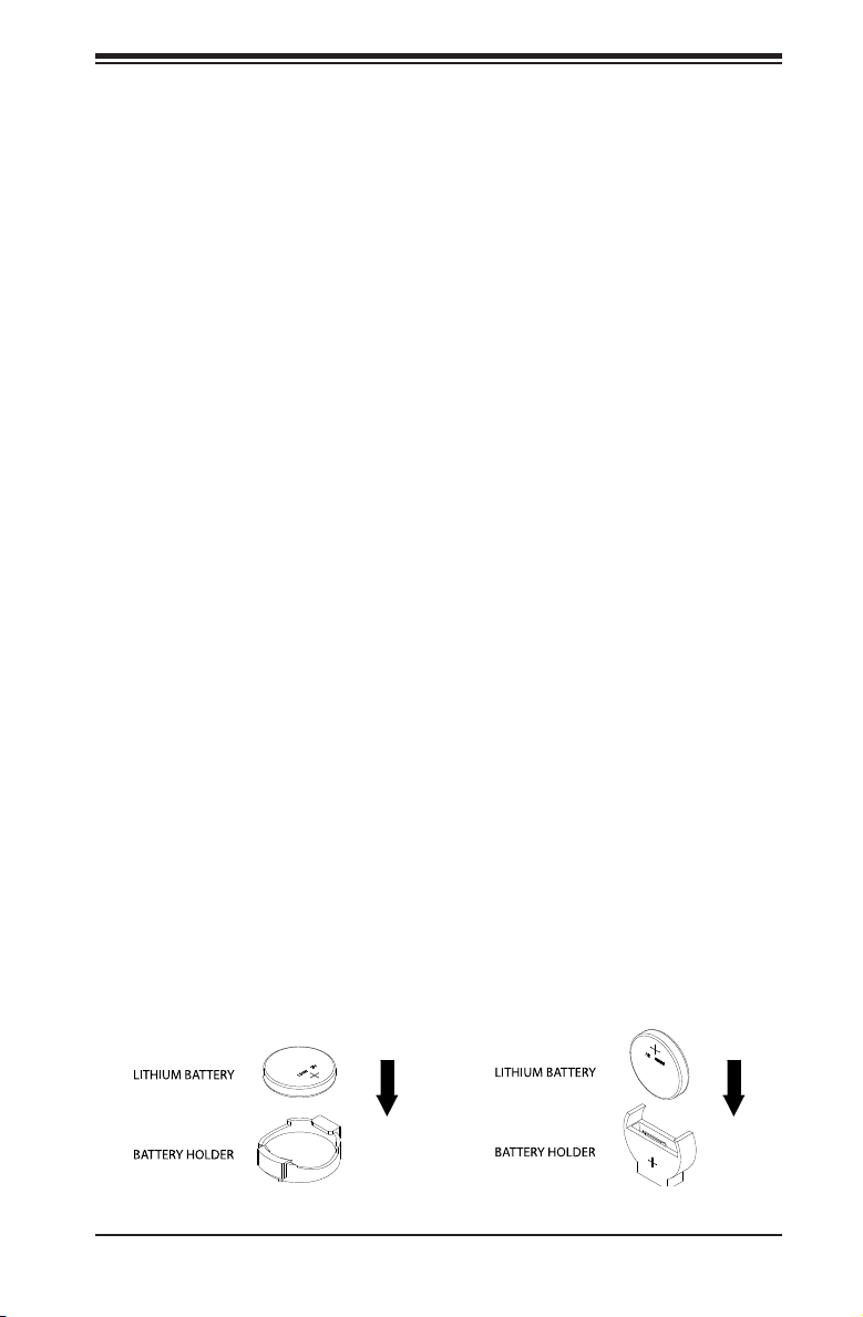
Chapter 3: Troubleshooting
3-3 Battery Removal and Installation
Battery Removal
To remove the onboard battery, follow the steps below:
1. Power off your system and unplug your power cable.
2. Locate the onboard battery as shown below.
3. Using a tool such as a pen or a small screwdriver, push the battery lock out-
wards to unlock it. Once unlocked, the battery will pop out from the holder.
4. Remove the battery.
Proper Battery Disposal
Warning: Please handle used batteries carefully. Do not damage the battery in any
way; a damaged battery may release hazardous materials into the environment. Do
not discard a used battery in the garbage or a public landll. Please comply with the
regulations set up by your local hazardous waste management agency to dispose of
your used battery properly.
Battery Installation
1. To install an onboard battery, follow the steps 1 & 2 above and continue
below:
2. Identify the battery's polarity. The positive (+) side should be facing up.
3. Insert the battery into the battery holder and push it down until you hear a
click to ensure that the battery is securely locked.
Warning: When replacing a battery, be sure to only replace it with the same type.
OR
3-5
Page 70

X9DRFF-i+/iT+/7+/7T+ Motherboard User’s Manual
3-4 Frequently Asked Questions
Question: What are the various types of memory that my motherboard can
support?
Answer: The motherboard supports Registered (RDIMM)/Load Reduced (LRDIMM)
ECC or Unbuffered (UDIMM) ECC/Non-ECC DDR3 modules. To enhance memory
performance, do not mix memory modules of different speeds, types, and sizes.
Please follow all memory installation instructions given on Section 2-4 in Chapter 2.
Question: How do I update my BIOS?
It is recommended that you do not upgrade your BIOS if you are not experiencing
any problems with your system. Updated BIOS les are located on our website
at http://www.supermicro.com. Please check our BIOS warning message and the
information on how to update your BIOS on our website. Select your motherboard
model and download the BIOS le to your computer. Also, check the current BIOS
revision to make sure that it is newer than your BIOS before downloading. You can
choose from the zip le and the .exe le. If you choose the zip BIOS le, please
unzip the BIOS le onto a bootable USB device. Run the batch le using the format
AMI.bat lename.rom from your bootable USB device to ash the BIOS. Then, your
system will automatically reboot.
Warning: Do not shut down or reset the system while updating the BIOS to prevent
possible system boot failure!)
Note: The SPI BIOS chip used on this motherboard cannot be removed.
Send your motherboard back to our RMA Department at Supermicro for
repair. For BIOS Recovery instructions, please refer to the AMI BIOS
Recovery Instructions posted at http://www.supermicro.com.
Question: How do I handle the used battery?
Answer: Please handle used batteries carefully. Do not damage the battery in any
way; a damaged battery may release hazardous materials into the environment.
Do not discard a used battery in the garbage or a public landll. Please comply
with the regulations set up by your local hazardous waste management agency to
dispose of your used battery properly. Refer to Section 3-3.
3-6
Page 71

Chapter 3: Troubleshooting
3-5 Returning Merchandise for Service
A receipt or copy of your invoice marked with the date of purchase is required before
any warranty service will be rendered. You can obtain service by calling your ven-
dor for a Returned Merchandise Authorization (RMA) number. When returning the
motherboard to the manufacturer, the RMA number should be prominently displayed
on the outside of the shipping carton, and the shipping package is mailed prepaid
or hand-carried. Shipping and handling charges will be applied for all orders that
must be mailed when service is complete. For faster service, you can also request
a RMA authorization online (http://www.supermicro.com/RmaForm/).
This warranty only covers normal consumer use and does not cover damages in-
curred in shipping or from failure due to the alternation, misuse, abuse or improper
maintenance of products.
During the warranty period, contact your distributor rst for any product problems.
3-7
Page 72

X9DRFF-i+/iT+/7+/7T+ Motherboard User’s Manual
Notes
3-8
Page 73

Chapter 4: AMI BIOS
Chapter 4
BIOS
4-1 Introduction
This chapter describes the AMI BIOS Setup utility for the X9DRFF-7/i. It also pro-
vides the instructions on how to navigate the AMI BIOS Setup utility screens. The
AMI ROM BIOS is stored in a Flash EEPROM and can be easily updated.
Starting BIOS Setup Utility
To enter the AMI BIOS Setup utility screens, press the <Del> key while the system
is booting up.
Note: In most cases, the <Del> key is used to invoke the AMI BIOS setup
screen. There are a few cases when other keys are used, such as <F3>,
<F4>, etc.
Each main BIOS menu option is described in this manual. The Main BIOS setup
menu screen has two main frames. The left frame displays all the options that can
be congured. Grayed-out options cannot be congured. Options in blue can be con-
gured by the user. The right frame displays the key legend. Above the key legend
is an area reserved for informational text related to the option currently selected in
the left frame. When an option is selected in the left frame, it is highlighted in white.
Note: The AMI BIOS has default informational messages built in. The
manufacturer retains the option to include, omit, or change any of these
messages.
The AMI BIOS Setup utility uses a key-based navigation system called "hot keys."
Most of the AMI BIOS setup utility "hot keys" can be used at any time during setup
navigation. These keys include <F3>, <F4>, <Enter>, <ESC>, arrow keys, etc.
Note 1: Options printed in Bold are default settings.
Note 2: <F3> is used to load optimal default settings. <F4> is used to save
the settings and exit the setup utility.
4-1
Page 74
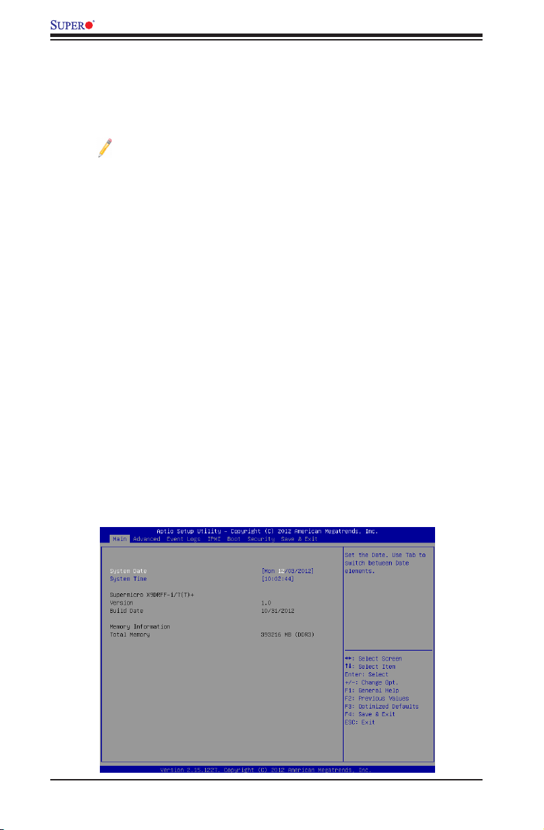
X9DRFF-i+/iT+/7+/7T+ Motherboard User’s Manual
HowToChangetheCongurationData
The conguration data that determines the system parameters may be changed by
entering the AMI BIOS Setup utility. This Setup utility can be accessed by pressing
<Delete> at the appropriate time during system boot.
Note: For AMI UEFI BIOS Recovery, please refer to the UEFI BIOS Re-
covery User Guide posted @http://www.supermicro.com/support/manuals/.
Starting the Setup Utility
Normally, the only visible Power-On Self-Test (POST) routine is the memory test.
As the memory is being tested, press the <Delete> key to enter the main menu of
the AMI BIOS Setup utility. From the main menu, you can access the other setup
screens. An AMI BIOS identication string is displayed at the left bottom corner of
the screen below the copyright message.
Warning: Do not upgrade the BIOS unless your system has a BIOS-related issue.
Flashing the wrong BIOS can cause irreparable damage to the system. In no event
shall the manufacturer be liable for direct, indirect, special, incidental, or consequential
damage arising from a BIOS update. If you have to update the BIOS, do not shut down
or reset the system while the BIOS is being updated to avoid possible boot failure.
4-2 Main Setup
When you rst enter the AMI BIOS Setup utility, you will enter the Main setup screen.
You can always return to the Main setup screen by selecting the Main tab on the
top of the screen. The Main BIOS Setup screen is shown below.
The AMI BIOS Main menu displays the following information:
4-2
Page 75

Chapter 4: AMI BIOS
System Date/System Time
Use this option to change the system time and date. Highlight System Time or
System Date using the arrow keys. Enter new values through the keyboard and
press <Enter>. Press the <Tab> key to move between elds. The date must be
entered in Day MM/DD/YY format. The time is entered in HH:MM:SS format. (Note:
The time is in the 24-hour format. For example, 5:30 P.M. appears as 17:30:00.).
Supermicro X9DRFF-i/7 (T)+
Version
This item displays the SMC version of the BIOS ROM used in this system.
Build Date
This item displays the date that the BIOS ROM was built.
Memory Information
Total Memory
This displays the amount of memory that is available in the system.
4-3
Page 76
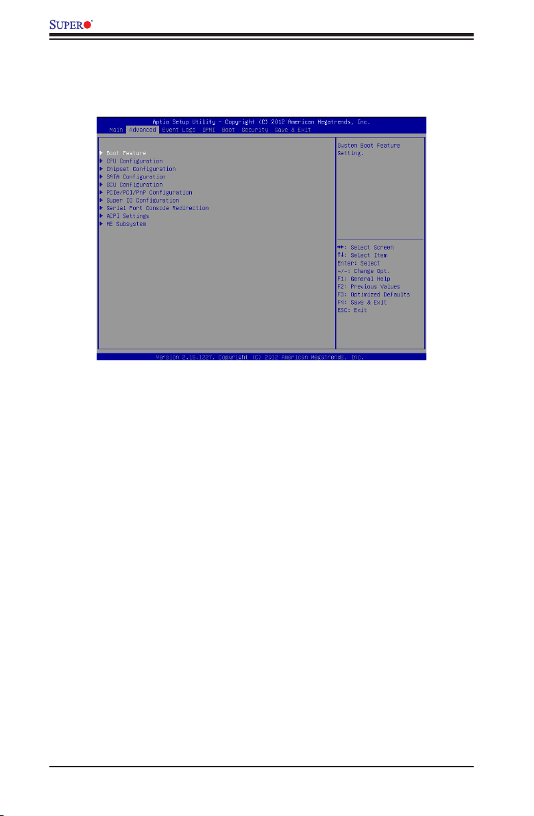
X9DRFF-i+/iT+/7+/7T+ Motherboard User’s Manual
4-3 AdvancedSetupCongurations
Select the Advanced tab to access the following submenu items.
Boot Feature
Quiet Boot
This feature allows the user to select bootup screen display between POST mes-
sages and the OEM logo. Select Disabled to display the POST messages. Select
Enabled to display the OEM logo instead of the normal POST messages. The op-
tions are Enabled and Disabled.
AddOn ROM Display Mode
Use this item to set the display mode for the Option ROM. Select Keep Current to
use the current AddOn ROM Display setting. Select Force BIOS to use the Option
ROM display mode set by the system BIOS. The options are Keep Current and
Force BIOS.
Bootup Num-Lock
Use this feature to set the Power-on state for the Numlock key. The options are
Off and On.
Wait For 'F1' If Error
Select Enabled to force the system to wait until the 'F1' key is pressed if an error
occurs. The options are Disabled and Enabled.
4-4
Page 77

Chapter 4: AMI BIOS
Interrupt 19 Capture
Interrupt 19 is the software interrupt that handles the boot disk function. When this
item is set to Enabled, the ROM BIOS of the host adaptors will "capture" Interrupt 19
at bootup and allow the drives that are attached to these host adaptors to function
as bootable disks. If this item is set to Disabled, the ROM BIOS of the host adap-
tors will not capture Interrupt 19, and the drives attached to these adaptors will not
function as bootable devices. The options are Enabled and Disabled.
Re-try Boot
When set to Enabled, the BIOS will continuously retry to boot from the selected
boot type. The options are Disabled, Legacy Boot, and EFI Boot.
PowerConguration
Watch Dog Function
If enabled, the Watch Dog timer will allow the system to automatically reboot when
a non-recoverable error occurs that lasts for more than ve minutes. The options
are Enabled and Disabled.
Power Button Function
If this feature is set to Instant Off, the system will power off immediately as soon
as the user presses the power button. If this feature is set to 4 Seconds Override,
the system will power off when the user presses the power button for 4 seconds or
longer. The options are Instant Off and 4 Seconds Override.
Restore on AC Power Loss
Use this feature to set the power state after a power outage. Select Stay Off for the
system power to remain off after a power loss. Select Power On for the system
power to be turned on after a power loss. Select Last State to allow the system
to resume its last state before a power loss. The options are Stay Off, Power On,
and Last State.
CPUConguration
This submenu displays the information of the CPU as detected by the BIOS. It also
allows the user to congure CPU settings.
Socket 1 CPU Information/Socket 2 CPU Information
This submenu displays the following information regarding the CPUs installed
in Socket 1/ Socket 2.
•Type of CPU
4-5
Page 78

X9DRFF-i+/iT+/7+/7T+ Motherboard User’s Manual
•CPU Signature
•Microcode Patch
•CPU Stepping
•Maximum / Minimum CPU Speed
•Processor Cores
•Intel HT (Hyper-Threading) Technology
•Intel VT-x Technology
•Intel SMX Technology
•L1 Data Cache / L1 Code Cache
•L2 Cache
•L3 Cache
CPU Speed
This item displays the speed of the CPU installed in Socket 1/Socket 2.
64-bit
This item indicates if the CPU installed in Socket 1 or Socket 2 supports 64-bit
technology.
Clock Spread Spectrum
Select Enable to enable Clock Spectrum support, which will allow the BIOS to moni-
tor and attempt to reduce the level of Electromagnetic Interference caused by the
components whenever needed. The options are Disabled and Enabled.
RTID (Record Types IDs)
This feature displays the total number of Record Type IDs for local and remote
pools. The options are Optimal and Alternate.
Hyper-threading
Select Enabled to support Intel Hyper-threading Technology to enhance CPU per-
formance. The options are Enabled and Disabled.
4-6
Page 79

Chapter 4: AMI BIOS
Active Processor Cores
Set to Enabled to use a processor's second core and above. (Please refer to Intel's
website for more information.) The options are All, 1, 2, 4, and 6.
Limit CPUID Maximum
This feature allows the user to set the maximum CPU ID value. Enable this function
to boot the legacy operating systems that cannot support processors with extended
CPUID functions. The options are Enabled and Disabled (for the Windows OS).
Execute-Disable Bit (Available if supported by the OS & the CPU)
Select Enabled to enable the Execute Disable Bit which will allow the processor
to designate areas in the system memory where an application code can execute
and where it cannot, thus preventing a worm or a virus from ooding illegal codes
to overwhelm the processor or damage the system during an attack. The default is
Enabled. (Refer to Intel and Microsoft Web sites for more information.)
Intel® AES-NI
Select Enable to use the Intel Advanced Encryption Standard (AES) New Instruc-
tions (NI) to ensure data security. The options are Enabled and Disabled.
MLC Streamer Prefetcher (Available when supported by the CPU)
If set to Enabled, the MLC (mid-level cache) streamer prefetcher will prefetch
streams of data and instructions from the main memory to the L2 cache to improve
CPU performance. The options are Disabled and Enabled.
MLC Spatial Prefetch (Available when supported by the CPU)
If this feature is set to Disabled, The CPU prefetches the cache line for 64 bytes.
If this feature is set to Enabled the CPU fetches both cache lines for 128 bytes as
comprised. The options are Disabled and Enabled.
DCU Streamer Prefetcher (Available when supported by the CPU)
Select Enabled to support Data Cache Unit (DCU) prefetch of L1 data to speed
up data accessing and processing in the DCU to enhance CPU performance. The
options are Disabled and Enabled.
DCU IP Prefetcher
Select Enabled for DCU (Data Cache Unit) IP Prefetcher support, which will prefetch
IP addresses to improve network connectivity and system performance. The options
are Enabled and Disabled.
4-7
Page 80

X9DRFF-i+/iT+/7+/7T+ Motherboard User’s Manual
Intel® Virtualization Technology (Available when supported by the CPU)
Select Enabled to support Intel Virtualization Technology, which will allow one
platform to run multiple operating systems and applications in independent parti-
tions, creating multiple "virtual" systems in one physical computer. The options
are Enabled and Disabled.
Note: If there is any change to this setting, you will need to reboot the
system for the change to take effect. Refer to Intel’s website for details.)
CPUPowerManagement Conguration
This submenu allows the user to congure the following CPU Power Manage-
ment settings.
Power Technology
Select Energy Efciency to support power-saving mode. Select Custom to cus-
tomize system power settings. Select Disabled to disable power-saving settings.
The options are Disabled, EnergyEfcient, and Custom. If the option is set to
Custom, the following items will display:
EIST (Available when Power Technology is set to Custom)
EIST (Enhanced Intel SpeedStep Technology) allows the system to au-
tomatically adjust processor voltage and core frequency to reduce power
consumption and heat dissipation. The options are Disabled, and Enabled.
Turbo Mode (Available when Power Technology is set to Custom and
EIST is set to Enabled)
Select Enabled to use the Turbo Mode to boost system performance. The
options are Enabled and Disabled.
C1E Support (Available when Power Technology is set to Custom)
Select Enabled to enable Enhanced C1 Power State to boost system per-
formance. The options are Enabled and Disabled.
CPU C3 Report (Available when Power Technology is set to Custom)
Select Enabled to allow the BIOS to report the CPU C3 State (ACPI C2) to
the operating system. During the CPU C3 State, the CPU clock generator
is turned off. The options are Enabled and Disabled.
4-8
Page 81

Chapter 4: AMI BIOS
CPU C6 Report (Available when Power Technology is set to Custom)
Select Enabled to allow the BIOS to report the CPU C6 State (ACPI C3) to
the operating system. During the CPU C6 State, the power to all cache is
turned off. The options are Enabled and Disabled.
CPU C7 Report (Available when Power Technology is set to Custom)
Select Enabled to allow the BIOS to report the CPU C7 State (ACPI C3) to
the operating system. CPU C7 State is a processor-specic low C-State.
The options are Enabled and Disabled.
Package C-State limit (Available when Power Technology is set to
Custom)
This feature allows the user to set the limit on the C-State package register.
The options are C0, C2, C6, and No Limit.
Energy/Performance Bias
Use this feature to select an appropriate fan setting to achieve maximum system
performance (with maximum cooling) or maximum energy efciency with maxi-
mum power saving). The fan speeds are controlled by the rmware management
via IPMI 2.0. The options are Performance, Balanced Performance, Balanced
Energy, and Energy Efcient.
Factory Long Duration Power Limit
This item displays the power limit (in watts) set by the manufacturer during which
long duration power is maintained.
Long Duration Power Limit
This item displays the power limit (in watts) set by the user during which long
duration power is maintained. The default setting is 0.
Factory Long Duration Maintained
This item displays the period of time (in seconds) set by the manufacturer during
which long duration power is maintained.
Long Duration Maintained
This item displays the period of time (in seconds) during which long duration
power is maintained. The default setting is 0.
4-9
Page 82

X9DRFF-i+/iT+/7+/7T+ Motherboard User’s Manual
Recommended Short Duration Power Limit
This item displays the short duration power settings (in watts) recommended by
the manufacturer.
Short Duration Power Limit
During Turbo Mode, the system may exceed the processors default power setting
and exceed the Short Duration Power limit. By increasing this value, the proces-
sor can provide better performance for short duration. This item displays the time
period during which short duration power is maintained. The default setting is 0.
ChipsetConguration
North Bridge
This feature allows the user to congure the settings for the Intel North Bridge.
IntegratedIO Conguration
Intel® VT-d
Select Enabled to enable Intel Virtualization Technology support for Direct I/O
VT-d by reporting the I/O device assignments to the VMM (Virtual Machine
Monitor) through the DMAR ACPI Tables. This feature offers fully-protected I/O
resource sharing across Intel platforms, providing greater reliability, security
and availability in networking and data-sharing. The options are Enabled and
Disabled.
Intel® I/OAT
Select Enabled to enable Intel I/OAT (I/O Acceleration Technology), which sig-
nicantly reduces CPU overhead by leveraging CPU architectural improvements
and freeing the system resource for other tasks. The options are Disabled and
Enabled.
DCA Support
When set to Enabled, this feature uses Intel's DCA (Direct Cache Access)
Technology to improve data transfer efciency. The options are Enabled and
Disabled.
IIO 1 PCIe Port Bifurcation Control
This submenu congures the following IO PCIe Port Bifurcation Control settings
for IIO 1 PCIe ports to determine how the available PCI-Express lanes to be
distributed between the PCI-Exp. Root Ports.
4-10
Page 83

Chapter 4: AMI BIOS
i350/X540 Link Speed
Select GEN1 to enable Generation 1 support for this port. Select GEN2 to enable
Generation 2 support for this port. Select GEN3 to enable Generation 3 support.
The options are GEN1, GEN2, and GEN3.
IOU1_2-PCIe Port
This feature allows the user to set the PCI-Exp bus speed between IOU3 and
PCI-e port. The options are x4x4x4x4, x4x4x8, x8x4x4, x8x8, and x16.
CPU1 SLOT1 Link Speed
Select GEN1 to enable Generation 1 support for this port. Select GEN2 to enable
Generation 2 support for this port. Select GEN3 to enable Generation 3 support.
The options are GEN1, GEN2, and GEN3.
IOU1_3-PCIe Port
This feature allows the user to set the PCI-Exp bus speed between IOU3 and
PCI-e port. The options are x4x4x4x4, x4x4x8, x8x4x4, x8x8, and x16.
LSI2208 Link Speed
Select GEN1 to enable Generation 1 support for this port. Select GEN2 to enable
Generation 2 support for this port. Select GEN3 to enable Generation 3 support.
The options are GEN1, GEN2, and GEN3.
CPU1 SLOT3 Link Speed
Select GEN1 to enable Generation 1 support for this port. Select GEN2 to enable
Generation 2 support for this port. Select GEN3 to enable Generation 3 support.
The options are GEN1, GEN2, and GEN3.
IIO 2 PCIe Port Bifurcation Control
This submenu congures the following IO PCIe Port Bifurcation Control settings
for IIO 1 PCIe ports to determine how the available PCI-Express lanes to be
distributed between the PCI-Exp. Root Ports.
IOU2_1-PCIe Port
This feature allows the user to set the PCI-Exp bus speed between IOU3 and
PCI-e port. The options are x4x4, and x8.
CPU2 SLOT4 Link Speed
Select GEN1 to enable Generation 1 support for this port. Select GEN2 to enable
Generation 2 support for this port. Select GEN3 to enable Generation 3 support.
The options are GEN1, GEN2, and GEN3.
4-11
Page 84

X9DRFF-i+/iT+/7+/7T+ Motherboard User’s Manual
IOU2_2-PCIe Port
This feature allows the user to set the PCI-Exp bus speed between IOU3 and
PCI-e port. The options are x4x4x4x4, x4x4x8, x8x4x4, x8x8, and x16.
CPU2 SXB1A Link Speed
Select GEN1 to enable Generation 1 support for this port. Select GEN2 to enable
Generation 2 support for this port. Select GEN3 to enable Generation 3 support.
The options are GEN1, GEN2, and GEN3.
IOU2_3-PCIe Port
This feature allows the user to set the PCI-Exp bus speed between IOU3 and
PCI-e port. The options are x4x4x4x4, x4x4x8, x8x4x4, x8x8, and x16.
CPU2 SXB1B Link Speed
Select GEN1 to enable Generation 1 support for this port. Select GEN2 to enable
Generation 2 support for this port. Select GEN3 to enable Generation 3 support.
The options are GEN1, GEN2, and GEN3.
QPIConguration
Current QPI Link
This item displays the current status of the QPI Link.
Current QPI Frequency
This item displays the frequency of the QPI Link.
Isoc
Select Enabled to enable Isochronous support to meet QoS (Quality of Service)
requirements. This feature is especially important for virtualization technology.
The options are Enabled and Disabled.
QPI (Quick Path Interconnect) Link Speed Mode
Use this feature to select data transfer speed for QPI Link connections. The
options are Slow and Fast.
QPI Link Frequency Select
Use this feature to select the desired QPI frequency. The options are Auto, 6.4
GT/s, 7.2 GT/s, and 8.0 GT/s.
4-12
Page 85

Chapter 4: AMI BIOS
DIMMConguration
This section displays the following DIMM information.
Current Memory Mode
This item displays the current memory mode.
Current Memory Speed
This item displays the current memory speed.
Mirroring
This item displays if memory mirroring is supported by the motherboard. Memory
mirroring creates a duplicate copy of the data stored in the memory to enhance
data security.
Sparing
This item displays if memory sparing is supported by the motherboard. Memory
sparing enhances system reliability, availability, and serviceability.
DIMM Information
CPU Socket 1 DIMM Information, CPU Socket 2 DIMM Information
The status of the memory modules detected by the BIOS will be displayed as
detected by the BIOS.
Memory Mode
When Independent is selected, all DIMMs are available to the operating system.
When Mirroring is selected, the motherboard maintains two identical copies of all
data in memory for data backup. When Lock Step is selected, the motherboard
uses two areas of memory to run the same set of operations in parallel. The
options are Independent, Mirroring, Lock Step, and Sparing.
DRAM RAPL Mode
RAPL (Running Average Power Limit) provides mechanisms to enforce power
consumption limits on supported processors The options are Disabled, DRAM
RAPL MODE0, and DRAM RAPL MODE1.
DDR Speed
Use this feature to force a DDR3 memory module to run at a frequency other than
what is specied in the specication. The options are Force DDR3-800, Force
DDR3-1066, Force DDR3-1333, Force DDR3-1600 and Force SPD, and Auto.
4-13
Page 86

X9DRFF-i+/iT+/7+/7T+ Motherboard User’s Manual
Channel Interleaving
This feature selects from the different channel interleaving methods. The options
are Auto, 1 Way, 2 Way, 3, Way, and 4 Way.
Rank Interleaving
This feature allows the user to select a rank memory interleaving method. The
options are Auto, 1 Way, 2 Way, 4, Way, and 8 Way.
Patrol Scrub
Patrol Scrubbing is a process that allows the CPU to correct correctable memory
errors detected on a memory module and send the correction to the requestor
(the original source). When this item is set to Enabled, the IO hub will read and
write back one cache line every 16K cycles, if there is no delay caused by internal
processing. By using this method, roughly 64 GB of memory behind the IO hub
will be scrubbed every day. The options are Enabled and Disabled.
Demand Scrub
Demand Scrubbing is a process that allows the CPU to correct correctable
memory errors found on a memory module. When the CPU or I/O issues a
demand-read command, and the read data from memory turns out to be a
correctable error, the error is corrected and sent to the requestor (the original
source). Memory is updated as well. Select Enabled to use Demand Scrubbing
for ECC memory correction. The options are Enabled and Disabled.
Data Scrambling
Select Enabled to enable data scrambling to ensure data security and integrity.
The options are Disabled and Enabled.
Device Tagging
Select Enabled to support device tagging. The options are Disabled and En-
abled.
Thermal Throttling
Throttling improves reliability and reduces power consumption in the proces-
sor via automatic voltage control during processor idle states. The options are
Disabled and CLTT (Closed Loop Thermal Throttling).
4-14
Page 87

Chapter 4: AMI BIOS
South Bridge
This feature allows the user to congure the settings for the Intel PCH chip.
PCH Information
This feature displays the following PCH information.
Name: This item displays the name of the PCH chip.
Stepping: This item displays the status of the PCH stepping.
USB Devices: This item displays the USB devices detected by the BIOS.
All USB Devices
This feature enables all USB ports/devices. The options are Disabled and Enabled.
(If set to Enabled, EHCI Controller 1 and Controller 2 will appear.)
EHCI Controller 1/EHCI Controller 2 (Available when All USB Devices is set
to Enabled)
Select Enabled to enable EHCI (Enhanced Host Controller Interface) Controller 1
or Controller 2. The options are Disabled and Enabled.
Legacy USB Support (Available when USB Functions is not Disabled)
Select Enabled to support legacy USB devices. Select Auto to disable legacy sup-
port if USB devices are not present. Select Disabled to have USB devices available
for EFI (Extensive Firmware Interface) applications only. The settings are Enabled
Disabled, and Auto.
Port 60/64 Emulation
Select Enabled to enable I/O port 60h/64h emulation support for the legacy USB
keyboard so that it can be fully supported by the operating systems that does not
recognize a USB device. The options are Disabled and Enabled.
EHCI Hand-Off
This item is for operating systems that do not support Enhanced Host Controller
Interface (EHCI) hand-off. When enabled, EHCI ownership change will be claimed
by the EHCI driver. The options are Disabled and Enabled.
4-15
Page 88

X9DRFF-i+/iT+/7+/7T+ Motherboard User’s Manual
SATAConguration
When this submenu is selected, the AMI BIOS automatically detects the presence
of IDE or SATA devices and displays the following items.
SATA Port0~SATA Port5: The AMI BIOS displays the status of each SATA port
as detected by the BIOS.
SATA Mode
Use this feature to congure SATA mode for a selected SATA port. The options are
Disabled, IDE Mode, AHCI Mode and RAID Mode. The following are displayed
depending on your selection:
IDE Mode
The following items are displayed when IDE Mode is selected:
Serial-ATA (SATA) Controller 0~1
Use this feature to activate or deactivate the SATA controller, and set the
compatibility mode. The options for SATA Controller 0 are Disabled, En-
hanced, and Compatible. The options for SATA Controller 1 are Disabled
and Enhanced.
AHCI Mode
The following items are displayed when the AHCI Mode is selected.
Aggressive Link Power Management
When Enabled, the SATA AHCI controller manages the power usage of
the SATA link. The controller will put the link in a low power mode during
extended periods of I/O inactivity, and will return the link to an active state
when I/O activity resumes. The options are Enabled and Disabled.
Port 0~5 Hot Plug
Select Enabled to enable hot-plug support for a particular port, which will
allow the user to change a hardware component or device without shutting
down the system. The options are Enabled and Disabled.
Staggered Spin Up
Select Enabled to enable Staggered Spin-up support to prevent excessive
power consumption caused by multiple HDDs spinning-up simultaneously.
The options are Enabled and Disabled.
4-16
Page 89

Chapter 4: AMI BIOS
RAID Mode
The following items are displayed when RAID Mode is selected:
SATA RAID Option ROM/UEFI Driver
Use this feature to enable the onboard SATA Option ROM or EFI driver. The
options are Disabled and Enabled..
Port 0~5 Hot Plug
Select Enabled to enable hot-plug support for the particular port. The options
are Enabled and Disabled.
SCU(StorageControlUnit)Conguration
Storage Controller Unit
Select Enabled to enable PCH SCU storage devices. The options are Disabled
and Enabled.
SCU RAID Option ROM
Select Enabled to support the onboard SCU Option ROM/UEFI Driver to boot up
the system via a storage device. The options are Disabled and Enabled.
SCU Port 0: The AMI BIOS will automatically detect the onboard SCU devices and
display the status of each SCU device as detected.
PCIe/PCI/PnPConguration
Launch Storage OpROM Policy
Use this feature to select the Option ROM to boot the system when there are
multiple Option ROMs available in the system. The options are Legacy ROM and
EFI Compatible ROM.
PCI Latency Timer
Use this feature to set the latency Timer of each PCI device installed on a PCI bus.
Select 64 to set the PCI latency to 64 PCI clock cycles. The options are 32, 64, 96,
128, 160, 192, 224 and 248.
PERR# Generation
Select Enabled to allow a PCI device to generate a PERR number for a PCI Bus
Signal Error Event. The options are Enabled and Disabled.
4-17
Page 90

X9DRFF-i+/iT+/7+/7T+ Motherboard User’s Manual
SERR# Generation
Select Enabled to allow a PCI device to generate an SERR number for a PCI Bus
Signal Error Event. The options are Enabled and Disabled.
Maximum Payload
Select Auto to allow the system BIOS to automatically set the maximum payload
value for a PCI-E device to enhance system performance. The options are Auto,
128 Bytes and 256 Bytes.
Maximum Read Request
Select Auto to allow the system BIOS to automatically set the maximum Read
Request size for a PCI-E device to enhance system performance. The options are
Auto, 128 Bytes, 256 Bytes, 512 Bytes, 1024 Bytes, 2048 Bytes, and 4096 Bytes.
ASPM Support
This feature allows the user to set the Active State Power Management (ASPM)
level for a PCI-E device. Select Force L0s to force all PCI-E links to operate at L0s
state. Select Auto to allow the system BIOS to automatically set the ASPM level for
the system. Select Disabled to disable ASPM support. The options are Disabled,
Auto, and Force L0s.
Warning: Enabling ASPM support may cause some PCI-E devices to fail!
CPU1 SLOT1 PCI-E 3.0 x16 OPROM, PCH SLOT2 PCI-E 2.0 x4 OPROM,
CPU1 SLOT3 PCI-E 3.0 x8 OPROM, CPU2 SLOT4 PCI-E 3.0 x8 OPROM,
CPU2 SXB1A PCI-E 3.0 x16 OPROM, CPU2 SXB1B PCI-E 3.0 x16 OPROM
Select Enabled to enable Option ROM support to boot the computer using a de-
vice installed on the slot specied above. The options are Enabled and Disabled.
Onboard LAN Option ROM Select
Select iSCSI to use the iSCSI Option ROM to boot the computer using a network
device. Select PXE (Preboot Execution Environment) to use an PXE Option ROM
to boot the computer using a network device. The options are PXE and iSCSI.
Load Onboard LAN 1 Option ROM, Load Onboard LAN 2 Option ROM
Select Enabled to enable the onboard LAN 1 or L AN 2 Option ROM. This is to boot
the computer using a network device. The default setting for LAN1 Option ROM is
Enabled, and the default setting for LAN2 Option ROM is Disabled.
Load Onboard SAS Option ROM
Select Enabled to use the onboard SAS Option ROM to boot the computer using
a SAS device. The options are Enabled and Disabled.
4-18
Page 91

Chapter 4: AMI BIOS
VGA Priority
This feature allows the user to select the graphics adapter to be used as the primary
boot device. The options are Onboard, and Offboard.
Network Stack
Select Enabled enable PXE (Preboot Execution Environment) or UEFI (Unied
Extensible Firmware Interface) for network stack support. The options are Enabled
and Disabled.
SuperIOConguration
Super IO Chip: This item displays the Super IO chip used in the motherboard.
COMConguration
Serial Port 2 Attribute
Use this feature to select the attribute for this serial port. The options are COM/
SOL (Serial Over LAN), and BMC.
Serial Port
Select Enabled to enable the COM serial port. The options are Enabled and Dis-
abled.
Device Settings
This item displays the settings of the COM serial port.
Change Settings
This option species the base I/O port address and the Interrupt Request address
of the COM serial port. Select Disabled to prevent the serial port from accessing
any system resources. When this option is set to Disabled, the serial port becomes
unavailable. The options are Auto, IO=3F8h; IRQ=4; IO=3F8h; IRQ=3; IO=2F8h;
IRQ=3; IO=3E8h; IRQ=5; IO=2E8h; IRQ=7; IO=3F8h; IRQ=3, 4, 5, 6, 7, 10, 11,
12; IO=2F8h; IRQ=3, 4, 5, 6, 7, 10, 11, 12; IO=3E8h; IRQ=3, 4, 5, 6, 7, 10, 11, 12;
IO=2E8h; IRQ=3, 4, 5, 6, 7, 10, 11, 12;
Device Mode
Use this feature to select the desired mode for a serial port specied. The options
are Normal and High Speed.
4-19
Page 92

X9DRFF-i+/iT+/7+/7T+ Motherboard User’s Manual
SOLConguration
Serial Port
Select Enabled to enable the SOL serial port. The options are Enabled and Dis-
abled.
Device Settings
This item displays the settings of the SOL serial port.
SOL Change Settings
This option species the base I/O port address and the Interrupt Request address
of the SOL Port. Select Disabled to prevent the serial port from accessing any
system resources. When this option is set to Disabled, the serial port becomes
unavailable. The options are Auto, IO=3F8h; IRQ=4; IO=3F8h; IRQ=3; IO=2F8h;
IRQ=3; IO=3E8h; IRQ=5; IO=2E8h; IRQ=7; IO=3F8h; IRQ=3, 4, 5, 6, 7, 10, 11,
12; IO=2F8h; IRQ=3, 4, 5, 6, 7, 10, 11, 12; IO=3E8h; IRQ=3, 4, 5, 6, 7, 10, 11, 12;
IO=2E8h; IRQ=3, 4, 5, 6, 7, 10, 11, 12;
SOL Device Mode
Use this feature to select the desired mode for a serial port specied. The options
are Normal and High Speed.
Serial Port Console Redirection
COM, SOL
These two submenus allow the user to congure the following Console Redirection
settings for a COM Port specied by the user.
COM Console Redirection, SOL Console Redirection
Select Enabled to use a COM Port selected by the user for Console Redirection.
The options are Enabled and Disabled. The default setting for COM is Disabled.
The default setting for SOL is Enabled.
Console Redirection Settings
This feature allows the user to specify how the host computer will exchange
data with the client computer, which is the remote computer used by the user.
Terminal Type
This feature allows the user to select the target terminal emulation type for Con-
sole Redirection. Select VT100 to use the ASCII Character set. Select VT100+ to
add color and function key support. Select ANSI to use the Extended ASCII Char-
4-20
Page 93

Chapter 4: AMI BIOS
acter Set. Select VT-UTF8 to use UTF8 encoding to map Unicode characters
into one or more bytes. The options are VT100, VT100+, VT-UTF8, and ANSI.
Bits Per second
Use this feature to set the transmission speed for a serial port used in Console
Redirection. Make sure that the same speed is used in the host computer and the
client computer. A lower transmission speed may be required for long and busy
lines. The options are 9600, 19200, 38400, 57600 and 115200 (bits per second).
Data Bits
Use this feature to set the data transmission size for Console Redirection. The
options are 7 Bits and 8 Bits.
Parity
A parity bit can be sent along with regular data bits to detect data transmission
errors. Select Even if the parity bit is set to 0, and the number of 1's in data bits
is even. Select Odd if the parity bit is set to 0, and the number of 1's in data bits
is odd. Select None if you do not want to send a parity bit with your data bits
in transmission. Select Mark to add a mark as a parity bit to be sent along with
the data bits. Select Space to add a Space as a parity bit to be sent with your
data bits. The options are None, Even, Odd, Mark and Space.
Stop Bits
A stop bit indicates the end of a serial data packet. Select 1 Stop Bit for standard
serial data communication. Select 2 Stop Bits if slower devices are used. The
options are 1 and 2.
Flow Control
This feature allows the user to set the ow control for Console Redirection to
prevent data loss caused by buffer overow. Send a "Stop" signal to stop send-
ing data when the receiving buffer is full. Send a "Start" signal to start sending
data when the receiving buffer is empty. The options are None and Hardware
RTS/CTS.
VT-UTF8 Combo Key Support
Select Enabled to enable VT-UTF8 Combination Key support for ANSI/VT100
terminals. The options are Enabled and Disabled.
Recorder Mode
Select Enabled to capture the data displayed on a terminal and send it as text
messages to a remote server. The options are Disabled and Enabled.
4-21
Page 94

X9DRFF-i+/iT+/7+/7T+ Motherboard User’s Manual
Resolution 100x31
Select Enabled for extended-terminal resolution support. The options are Dis-
abled and Enabled.
Legacy OS Redirection Resolution
Use this feature to select the number of rows and columns used in Console
Redirection for legacy OS support. The options are 80x24 and 80x25.
Putty KeyPad
This feature selects Function Keys and KeyPad settings for Putty, which is a
terminal emulator designed for the Windows OS. The options are VT100, LINUX,
XTERMR6, SCO, ESCN, and VT400.
Redirection After BIOS POST
Select Always Enable to keep Console Redirection active all the time after
POST (Power-On Self-Test). Select BootLoader to keep Console Redirection
active during POST and Boot Loader. The options are Always Enable and
BootLoader.
Serial Port for Out-of-Band Management/Windows Emergency Management
Services (EMS)
The submenu allows the user to congure Console Redirection settings to support
Out-of-Band Serial Port management.
EMS Console Redirection
Select Enabled to use a COM Port selected by the user for Console Redirection.
The options are Enabled and Disabled.
Console Redirection Settings (for EMS)
This feature allows the user to specify how the host computer will exchange
data with the client computer, which is the remote computer used by the user.
Out-of-Band Management Port
The feature selects a serial port used by the Microsoft Windows Emergency
Management Services (EMS) to communicate with a remote server. The options
are COM and SOL.
Terminal Type
This feature allows the user to select the target terminal emulation type for Con-
sole Redirection. Select VT100 to use the ASCII character set. Select VT100+ to
add color and function key support. Select ANSI to use the extended ASCII char-
4-22
Page 95

Chapter 4: AMI BIOS
acter set. Select VT-UTF8 to use UTF8 encoding to map Unicode characters into
one or more bytes. The options are VT100, VT100+, and VT-UTF8, and ANSI.
Bits Per Second
This item sets the transmission speed for a serial port used in Console Redirec-
tion. Make sure that the same speed is used in the host computer and the client
computer. A lower transmission speed may be required for long and busy lines.
The options are 9600, 19200, 57600, and 115200 (bits per second).
Flow Control
This feature allows the user to set the ow control for Console Redirection to
prevent data loss caused by buffer overow. Send a "Stop" signal to stop send-
ing data when the receiving buffer is full. Send a "Start" signal to start sending
data when the receiving buffer is empty. The options are None, Hardware RTS/
CTS, and Software Xon/Xoff.
Data Bits, Parity, Stop Bits
The setting for each of these features is displayed.
ACPI Settings
Use this feature to congure Advanced Conguration and Power Interface (ACPI)
power management settings for your system.
ACPI Sleep State
Use this feature to select the ACPI State when the system is in sleep mode. Select
S1 (CPU Stop Clock) to erase all CPU caches and stop executing instructions.
Power to the CPU(s) and RAM is maintained, but RAM is refreshed. Select Sus-
pend Disabled to use power-reduced mode. Power will only be supplied to limited
components (such as RAMs) to maintain the most critical functions of the system.
The options are Suspend Disabled and S1 (CPU Stop Clock).
NUMA (NON-Uniform Memory Access)
This feature enables the Non-Uniform Memory Access ACPI support. The options
are Enabled and Disabled.
High Precision Event Timer
Select Enabled to activate the High Precision Event Timer (HPET) that produces
periodic interrupts at a much higher frequency than a Real-time Clock (RTC) does
in synchronizing multimedia streams, providing smooth playback, reducing the de-
pendency on other timestamp calculation devices, such as an x86 RDTSC Instruc-
tion embedded in the CPU. The High Performance Event Timer is used to replace
the 8254 Programmable Interval Timer. The options are Enabled and Disabled.
4-23
Page 96
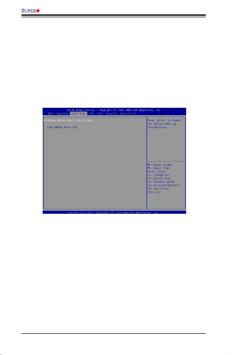
X9DRFF-i+/iT+/7+/7T+ Motherboard User’s Manual
ME Subsystem
This feature displays the following ME Subsystem Conguration settings.
•ME BIOS Interface Version
•ME Version
4-4 Event Logs
Select the Event Logs tab to access the following submenu items.
Change SMBIOS Event Log Settings
This feature allows the user to congure SMBIOS Event settings.
Enabling/Disabling Options
SMBIOS Event Log
Select Enabled to enable SMBIOS (System Management BIOS) Event Logging
during system boot. The options are Enabled and Disabled.
Runtime Error Logging Support
Select Enabled to support Runtime Error Logging. The options are Enabled and
Disabled.
4-24
Page 97

Chapter 4: AMI BIOS
Memory Correctable Error Threshold
This feature allows the user to enter the threshold value for correctable memory
errors. The default setting is 10.
PCI Error Logging Support
Select Enabled to support error event logging for PCI slots. The options are Enabled
and Disabled.
Erasing Settings
Erase Event Log
Select Enabled to erase the SMBIOS (System Management BIOS) Event Log, which
is completed before a event logging is initialized upon system reboot. The options
are No, Yes, Next reset, and Yes, Every reset.
When Log is Full
Select Erase Immediately to immediately erase SMBIOS error event logs that ex-
ceed the limit when the SMBIOS event log is full. Select Do Nothing for the system
to do nothing when the SMBIOS event log is full. The options are Do Nothing and
Erase Immediately.
SMBIOS Event Log Standard Settings
Log System Boot Event
Select Enabled to log system boot events. The options are Disabled and Enabled.
MECI (Multiple Event Count Increment)
Enter the increment value for the multiple event counter. Enter a number from 1 to
255. The default setting is 1.
METW (Multiple Event Count Time Window)
This item allows the user to decide how long (in minutes) should the multiple event
counter wait before generating a new event log. Enter a number from 0 to 99. The
default setting is 60.
View SMBIOS Event Log
This item allows the user to view the event in the SMBIOS event log. Select this
item and press <Enter> to view the status of an event in the log.
Date/Time/Error Code/Severity
4-25
Page 98
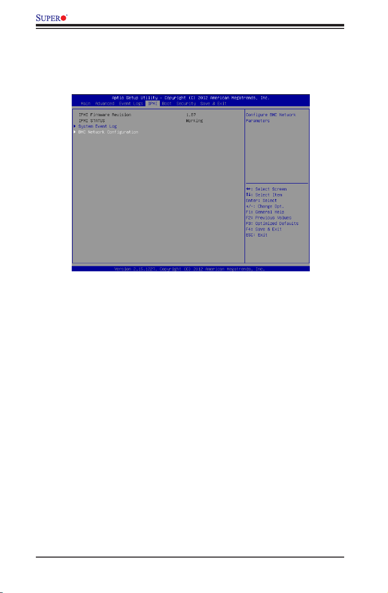
X9DRFF-i+/iT+/7+/7T+ Motherboard User’s Manual
4-5 IPMI
Select the IPMI (Intelligent Platform Management Interface) tab to access the fol-
lowing submenu items.
IPMI Firmware Revision
This item indicates the IPMI rmware revision used in your system.
IPMI Status
This item indicates the status of the IPMI rmware installed in your system.
System Event Log
Enabling/Disabling Options
SEL Components
Select Enabled for all system event logging at bootup. The options are Enabled
and Disabled.
Erasing Settings
Erase SEL
Select Yes, On next reset to erase all system event logs upon next system reboot.
Select Yes, On every reset to erase all system event logs upon each system reboot.
Select No to keep all system event logs after each system reboot. The options are
No, Yes, On next reset, and Yes, On every reset.
4-26
Page 99

Chapter 4: AMI BIOS
When SEL is Full
This feature allows the user to decide what the BIOS should do when the system
event log is full. Select Erase Immediately to erase all events in the log when the
system event log is full. The options are Do Nothing and Erase Immediately.
BMCNetworkConguration
IPMI LAN Selection
This item displays the LAN selection type. The default is Failover.
IPMI Network Link Status
This item displays the IPMI netowork link status.
UpdateIPMILANConguration
This feature allows the BIOS to implement any IP/MAC address changes at the next
system boot. If the option is set to Yes, any changes made to the settings below will
take effect when the system is rebooted. The options are No and Yes.
CongurationAddressSource
This feature allows the user to select the source of the IP address for this computer.
If Static is selected, you will need to know the IP address of this computer and enter
it to the system manually in the eld. If DHCP is selected, the BIOS will search for
a DHCP (Dynamic Host Conguration Protocol) server in the network that is at-
tached to and request the next available IP address for this computer. The options
are DHCP and Static. The following items are assigned IP addresses automatically
if DHCP is selected, or can be congured manually if Static is selected.
Station IP Address
This item displays the Station IP address for this computer. This should be in decimal
and in dotted quad form (i.e., 192.168.10.253).
Subnet Mask
This item displays the sub-network that this computer belongs to. The value of each
three-digit number separated by dots should not exceed 255.
Station MAC Address
This item displays the Station MAC address for this computer. Mac addresses are
6 two-digit hexadecimal numbers.
Gateway IP Address
This item displays the Gateway IP address for this computer. This should be in
decimal and in dotted quad form (i.e., 192.168.10.253).
4-27
Page 100
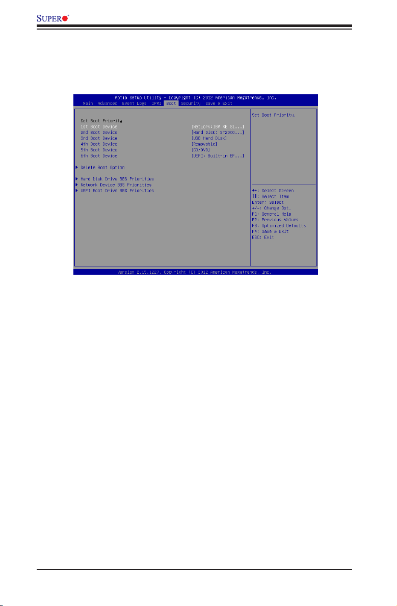
X9DRFF-i+/iT+/7+/7T+ Motherboard User’s Manual
4-6 Boot
This submenu allows the user to congure the following boot settings for the
system.
Set Boot Priorit y
1st Boot Device, 2nd Boot Device, etc.
Use this feature to specif y the sequence of boot device priority.
Delete Boot Option
This feature allows the user to select a EFI boot device to delete from the boot
priority list.
Delete Boot Option
Select the desired boot device to delete.
Hard Disk Drive BBS Priorities, Network Device BBS Priorities, UEFI Boot
Drive BBS Priorities
Use these options to set the order of the legacy network devices detected by the
motherboard.
4-28
 Loading...