

Page 1

X8QB6-F
X8QBE-F
USER’S MANUAL
Revision 1.1b
Page 2

The information in this User’s Manual has been carefully reviewed and is believed to be accurate.
The vendor assumes no responsibility for any inaccuracies that may be contained in this document,
and makes no commitment to update or to keep current the information in this manual, or to notify
any person or organization of the updates. Please Note: For the most up-to-date version of this
manual, please see our Website at www.supermicro.com.
Super Micro Computer, Inc. ("Supermicro") reserves the right to make changes to the product
described in this manual at any time and without notice. This product, including software and documentation, is the property of Supermicro and/or its licensors, and is supplied only under a license.
Any use or reproduction of this product is not allowed, except as expressly permitted by the terms
of said license.
IN NO EVENT WILL SUPER MICRO COMPUTER, INC. BE LIABLE FOR DIRECT, INDIRECT,
SPECIAL, INCIDENTAL, SPECULATIVE OR CONSEQUENTIAL DAMAGES ARISING FROM THE
USE OR INABILITY TO USE THIS PRODUCT OR DOCUMENTATION, EVEN IF ADVISED OF
THE POSSIBILITY OF SUCH DAMAGES. IN PARTICULAR, SUPER MICRO COMPUTER, INC.
SHALL NOT HAVE LIABILITY FOR ANY HARDWARE, SOFTWARE, OR DATA STORED OR USED
WITH THE PRODUCT, INCLUDING THE COSTS OF REPAIRING, REPLACING, INTEGRATING,
INSTALLING OR RECOVERING SUCH HARDWARE, SOFTWARE, OR DATA.
Any disputes arising between the manufacturer and the customer shall be governed by the laws of
Santa Clara County in the State of California, USA. The State of California, County of Santa Clara
shall be the exclusive venue for the resolution of any such disputes. Supermicro's total liability for
all claims will not exceed the price paid for the hardware product.
FCC Statement: This equipment has been tested and found to comply with the limits for a Class
A digital device pursuant to Part 15 of the FCC Rules. These limits are designed to provide
reasonable protection against harmful interference when the equipment is operated in a commercial
environment. This equipment generates, uses, and can radiate radio frequency energy and, if not
installed and used in accordance with the manufacturer’s instruction manual, may cause harmful
interference with radio communications. Operation of this equipment in a residential area is likely
to cause harmful interference, in which case you will be required to correct the interference at your
own expense.
California Best Management Practices Regulations for Perchlorate Materials: This Perchlorate
warning applies only to products containing CR (Manganese Dioxide) Lithium coin cells. “Perchlorate
Material-special handling may apply. See www.dtsc.ca.gov/hazardouswaste/perchlorate”.
WARNING: Handling of lead solder materials used in this
product may expose you to lead, a chemical known to
the State of California to cause birth defects and other
reproductive harm.
Manual Revision 1.1b
Release Date: January 7, 2011
Unless you request and receive written permission from Super Micro Computer, Inc., you may not
copy any part of this document.
Information in this document is subject to change without notice. Other products and companies
referred to herein are trademarks or registered trademarks of their respective companies or mark
holders.
Copyright © 2011 by Super Micro Computer, Inc.
All rights reserved.
Printed in the United States of America
Page 3

Preface
This manual is written for system integrators, PC technicians and
knowledgeable PC users. It provides information for the installation and use of the
X8QB6-F/X8QBE-F motherboard.
About This Motherboard
The X8QB6-F/X8QBE-F motherboard supports the Intel 7500 Series Socket-LS
processor, the fi rst generation chip multiprocessor (CMP) platform that offers Intel
QuickPath Interconnect (QPI) Technology, providing point-to-point system interface,
replacing the Front Side Bus. Integrating Intel Turbo Boost Technology, 45nm Process Technology, combined with support of up to 32 CPU cores and 24MB L3 cache,
the X8QB6-F/X8QBE-F motherboard substantially enhances system performance
for HPC/Cluster/Database server platforms. Please refer to our Website (http://www .
supermicro.com) for updates on supported processors. This product is intended to
be installed and serviced by professional technicians.
Preface
Manual Organization
Chapter 1 provides quick installation instructions.
Chapter 2 describes the features, specifi cations and performance of the mother-
board, and provides detailed information about the Intel 7500 chipset.
Chapter 3 provides hardware installation instructions. Read this chapter when in-
stalling the processor, memory modules and other hardware components into the
system. If you encounter any problems, see Chapter 4, which describes troubleshooting procedures for video, memory, and system setup stored in the CMOS.
Chapter 5 includes an introduction to the BIOS, and provides detailed information
on running the CMOS Setup utility.
Appendix A provides BIOS Error Beep Codes.
Appendix B lists Software Installation Instructions.
iii
Page 4
X8QB6-F/X8QBE-F Motherboard User’s Manual
Conventions Used in the Manual
Special attention should be given to the following symbols for proper installation
and to prevent damage to the system or injury to yourself:
Danger/Caution: Instructions to be strictly followed to prevent catastrophic
system failure or to avoid bodily injury
Warning: Important information given to ensure proper system installation
or to prevent damage to the components
Note: Additional information given to differentiate between various models
or provides information for correct system setup.
iv
Page 5

Contacting Supermicro
Headquarters
Address: Super Micro Computer, Inc.
980 Rock Ave.
San Jose, CA 95131 U.S.A.
[email protected] (Technical Support)
Website: www.supermicro.com
Europe
Address: Super Micro Computer B.V.
Preface
Het Sterrenbeeld 28, 5215 ML
's-Hertogenbosch, The Netherlands
[email protected] (Technical Support)
[email protected] (Customer Support)
Asia-Pacifi c
Address: Super Micro Computer, Inc.
4F, No. 232-1, Liancheng Rd.
Chung-Ho 235, Taipei County
Taiwan, R.O.C.
Tel: +886-(2) 8226-3990
Fax: +886-(2) 8226-3991
Website: www.supermicro.com.tw
Technical Support:
Email: [email protected]
Tel: 886-2-8228-1366, ext.132 or 139
v
Page 6

X8QB6-F/X8QBE-F Motherboard User’s Manual
Table of Contents
Preface
Chapter 1 Quick Installation Guide
1-1 Installing the CPU ...........................................................................................1-1
1-2 Installing the CPU/Heatsink/ CPU Fans ......................................................... 1-1
1-3 Installing the Memory Modules .......................................................................1-2
1-4 Installing the I/O Shield ................................................................................... 1-2
1-5 Installing the Motherboard ..............................................................................1-3
1-6 Connecting the Power Supply.........................................................................1-3
1-7 Installing Internal Peripherals ..........................................................................1-4
1-8 Installing External Peripherals ........................................................................1-4
Chapter 2 Overview
2-1 Overview ......................................................................................................... 2-1
Checklist ..........................................................................................................2-1
X8QB6-F/X8QBE-F Quick Reference .............................................................2-4
Motherboard Features .....................................................................................2-7
2-2 Chipset Overview ...........................................................................................2-11
2-3 Special Features ...........................................................................................2-12
2-4 PC Health Monitoring .................................................................................... 2-12
2-5 ACPI Features ...............................................................................................2-13
2-6 Power Supply ................................................................................................ 2-13
2-7 Super I/O ....................................................................................................... 2-14
2-8 Overview of the Nuvoton WPCM450R Controller .......................................2-14
Chapter 3 Installation
3-1 Static-Sensitive Devices ..................................................................................3-1
Precautions .....................................................................................................3-1
Unpacking .......................................................................................................3-1
3-2 Processor and Heatsink Installation................................................................3-2
Installing an LGA 1567 Processor .................................................................. 3-2
Installing a Passive CPU Heatsink ................................................................. 3-4
Removing the Passive Heatsink ..................................................................... 3-5
3-3 Installing and Removing the Memory Modules ...............................................3-6
Installing & Removing DIMMs .........................................................................3-6
Removing Memory Modules ........................................................................... 3-6
3-4 Motherboard Installation ..................................................................................3-9
Tools Needed .................................................................................................. 3-9
Location of Mounting Holes ............................................................................ 3-9
Installing the Motherboard ............................................................................3-10
vi
Page 7

Table of Contents
3-5 Control Panel Connectors/I/O Ports...............................................................3-11
Back Panel Connectors/I/O Ports ..................................................................3-11
Back Panel I/O Port Locations and Defi nitions ............................................3-1 1
Serial Ports ............................................................................................... 3-12
Video Connection ..................................................................................... 3-12
Universal Serial Bus (USB) ...................................................................... 3-13
Ethernet Ports .......................................................................................... 3-14
Unit Identifi er Switch ................................................................................3-15
Front Control Panel ....................................................................................... 3-16
Front Control Panel Pin Defi nitions............................................................... 3-17
NMI Button ............................................................................................... 3-17
Power LED .............................................................................................. 3-17
HDD LED .................................................................................................. 3-18
NIC1/NIC2 LED Indicators ....................................................................... 3-18
Overheat (OH)/Fan Fail/PWR Fail/UID LED ............................................ 3-19
Power Fail LED ........................................................................................3-19
Reset Button ........................................................................................... 3-20
Power Button ........................................................................................... 3-20
3-6 Connecting Cables ........................................................................................ 3-21
Power Connectors ...................................................................................3-21
Fan Headers ............................................................................................. 3-22
Chassis Intrusion .....................................................................................3-22
Internal Speaker ....................................................................................... 3-23
Power LED/Speaker ................................................................................. 3-23
TPM Header/Port 80 ................................................................................ 3-24
Overheat LED/Fan Fail ............................................................................3-24
Power SMB (I
2
C) Connector .................................................................... 3-25
IPMB .........................................................................................................3-25
T-SGPIO 1/2 Headers .............................................................................. 3-26
Wake-On-Ring ..........................................................................................3-26
BBU Header (Optional for the X8QB6-F Only) ........................................ 3-27
Unit Identifi cation Switch/LED .................................................................. 3-28
3-7 Jumper Settings ............................................................................................3-29
Explanation of Jumpers ................................................................................3-29
GLAN Enable/Disable ..............................................................................3-29
CMOS Clear ............................................................................................. 3-30
Watch Dog Enable/Disable ...................................................................... 3-30
VGA Enable .............................................................................................. 3-31
TPM Support Enable ................................................................................ 3-31
vii
Page 8

X8QB6-F/X8QBE-F Motherboard User’s Manual
SAS2 Enable (X8QB6-F only) ..................................................................3-32
BMC Enable ............................................................................................ 3-32
BMC Reset .............................................................................................. 3-33
3-8 Onboard LED Indicators ...............................................................................3-34
GLAN LEDs .............................................................................................. 3-34
IPMI Dedicated LAN LEDs .......................................................................3-34
Rear UID LED ......................................................................................... 3-35
BMC Heartbeat LED ................................................................................3-35
Onboard Power LED ............................................................................... 3-36
3-9 Serial ATA Connections ................................................................................. 3-37
Serial ATA Ports........................................................................................ 3-37
SAS2 Ports (X8QB6-F only).....................................................................3-37
Chapter 4 Troubleshooting
4-1 Troubleshooting Procedures ...........................................................................4-1
4-2 Technical Support Procedures ........................................................................4-4
4-3 Frequently Asked Questions ...........................................................................4-5
4-4 Returning Merchandise for Service.................................................................4-6
Chapter 5 BIOS
5-1 Introduction ...................................................................................................... 5-1
Starting BIOS Setup Utility ..............................................................................5-1
How To Change the Confi guration Data ......................................................... 5-1
Starting the Setup Utility ................................................................................. 5-2
5-2 Main Setup ......................................................................................................5-2
5-3 Advanced Setup Confi gurations...................................................................... 5-4
5-4 Boot Confi guration ........................................................................................5-29
5-5 Security Settings ........................................................................................... 5-30
5-6 Exit Options ................................................................................................... 5-31
Appendix A BIOS Error Beep Codes
A-1 BIOS Error Beep Codes ................................................................................. A-1
Appendix B Software Installation Instructions
B-1 Installing Software Programs ..........................................................................B-1
B-2 Confi guring Supero Doctor III .........................................................................B-2
viii
Page 9

Quick Installation Guide
1-1 Installing the CPU
2
A B
1
Chapter 1: Quick Installation Guide
Chapter 1
CPU Key
A. Press the socket clip down to unlock
it. Gently lift the socket clip to open the
load plate.
C
CPU Pin 1
C. Align CPU Pin 1 against Socket Pin
1. Once they are aligned, lower the CPU
down to the socket.
To avoid damage, do not rub the CPU pins against the socket.
B. Align the CPU key with the socket
key.
D
D. Once the CPU is fully seated on
the socket, press the socket clip down
to lock it.
1-2 Installing the CPU/Heatsink/ CPU Fans
A B
C
A. Apply the appropriate amount of ther-
mal grease (to 0.13mm in thickness).
B. Insert the two push-pins on the sides
of the heatsink into the mounting holes
on the motherboard, turning clockwise
to lock them.
C. Connect the fan cables to CPU
Fan1 and CPU Fan 2 headers.
1-1
Page 10
X8QB6-F/X8QBE-F Motherboard User’s Manual
1-3 Installing the Memory Modules
A B C
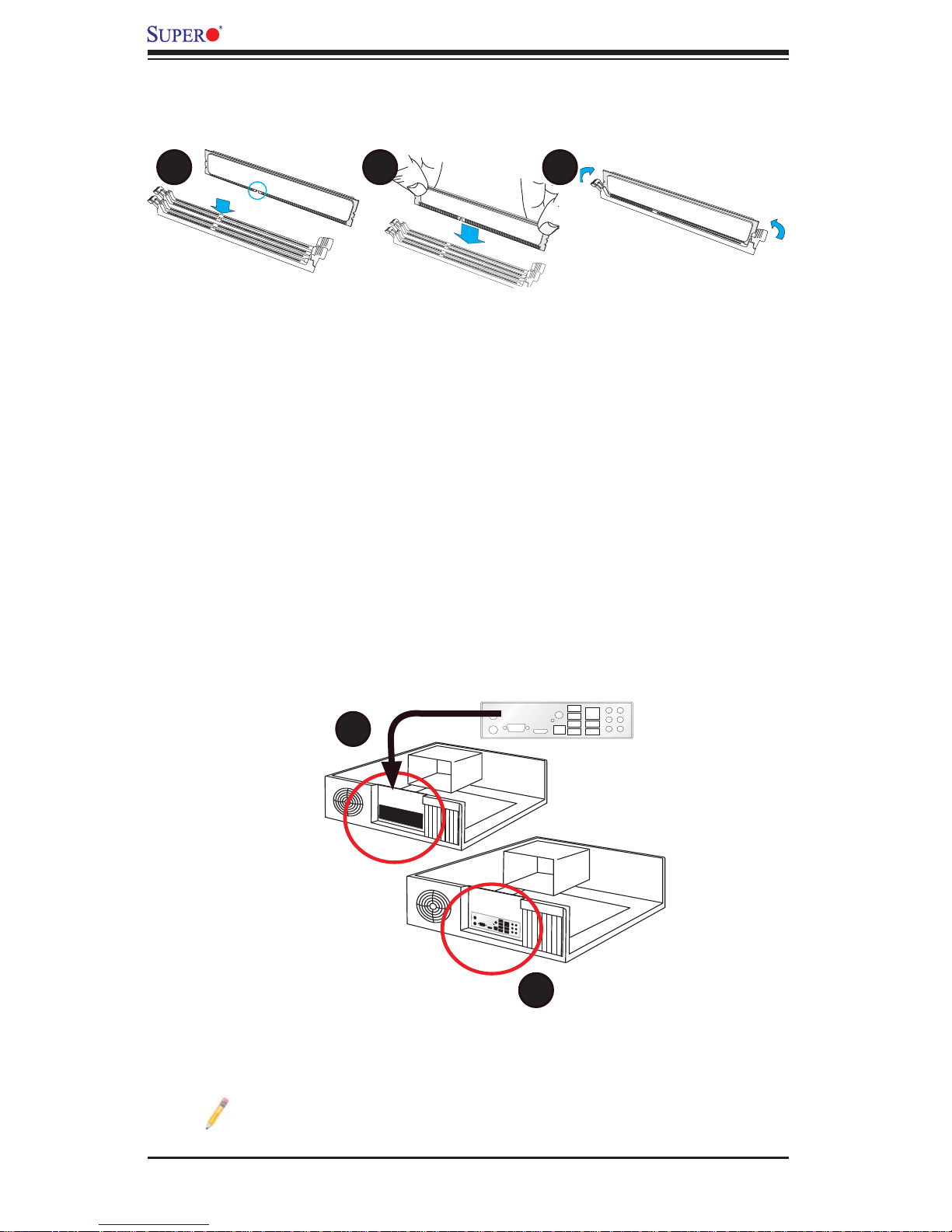
A. Press the release tabs on the both
ends of the DIMM socket outwards to
unlock it.
Align the key on the DIMM module
against that of the DIMM socket.
1-4 Installing the I/O Shield
A
B. Use two thumbs to press both
notches of the module straight down
into the DIMM socket.
C. Press the release tabs on the
ends of the DIMM module inwards
to lock it.
Note: Chassis and I/O plate images are for illustration purposes only . They
may be different from what you have in your system.
B
1-2
Page 11

1-5 Installing the Motherboard
A
X8QBE-F
Rev. 1.11
Chapter 1: Quick Installation Guide
B
C
1-6 Connecting the Power Supply
D
X8QBE-F
Rev. 1.11
B
A
Note: Please connect the 24-pin
power connector and three of the
four 8-pin power connectors to the
power supply to provide adequate
power supply to your system.
1-3
Page 12
X8QB6-F/X8QBE-F Motherboard User’s Manual
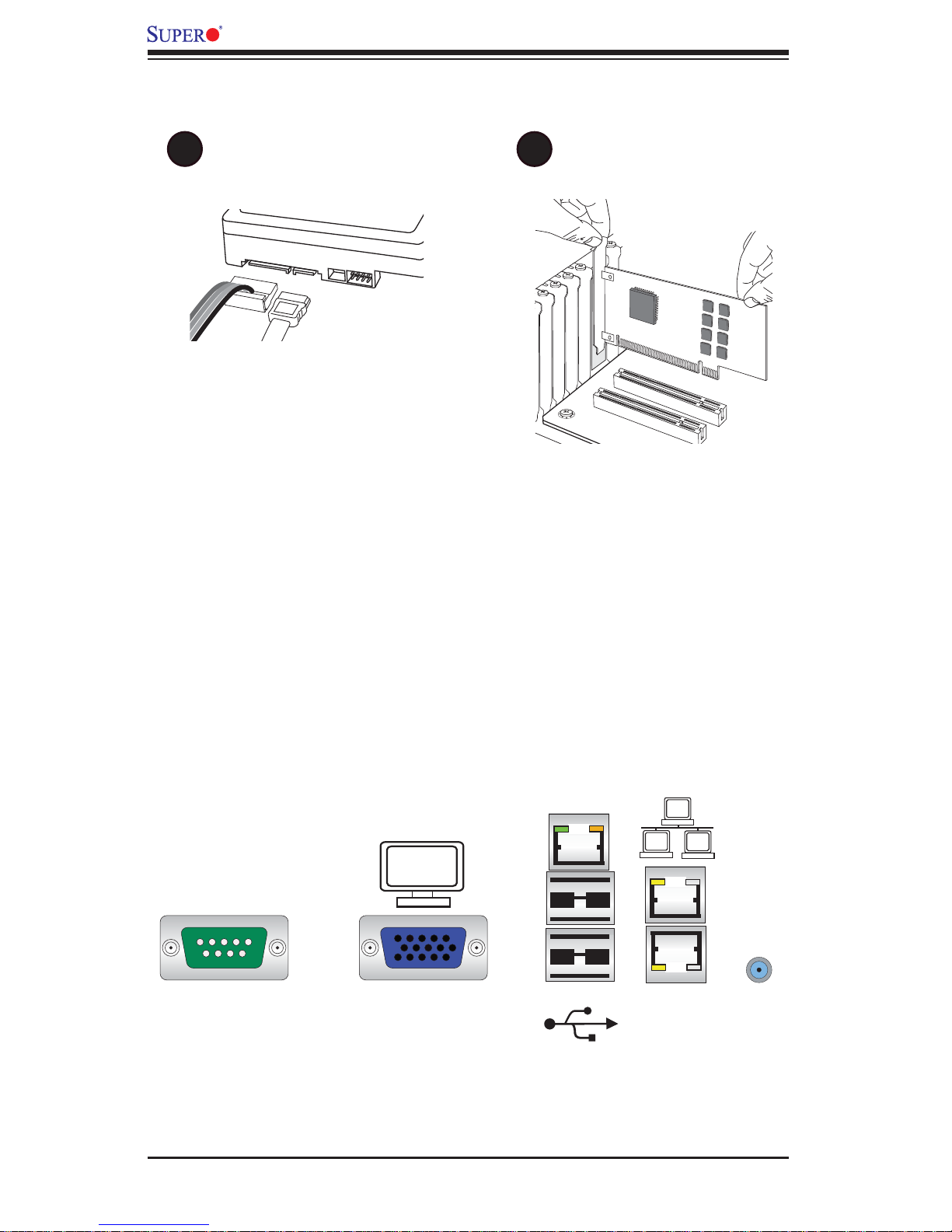
1-7 Installing Internal Peripherals
A
SATA/SAS2 Drives
B
Add-on Cards
1-8 Installing External Peripherals
Serial Port
(COM1)
VGA Port LAN 1/2 PortsUSB 0/1 UID
IPMI LAN
Switch
1-4
Page 13

Chapter 2: Overview
Chapter 2
Overview
2-1 Overview
Checklist
Congratulations on purchasing your computer motherboard from an acknowledged
leader in the industry. Supermicro boards are designed with the utmost attention to
detail to provide you with the highest standards in quality and performance.
Please check that the following items have all been included with your motherboard.
If anything listed here is damaged or missing, contact your retailer.
The following items are included in the retail box.
One (1) Supermicro Mainboard
•
Six (6) Serial ATA cables (CBL-0044Lx6) (for X8QBE-F)•
Two (2) I-Pass to 4 Serial ATA (50-cm) cables (CBL-097L-02) (for X8QB6-F)•
One (1) Supermicro CD containing drivers and utilities•
One (1) User's/BIOS Manual (MNL#1178)•
Optional (Required for Extended Battery Backup Support - X8QB6-F only)
The items listed below are available for purchase at Supermicro.
One (1) iBBU07 Battery (BTR-0018L-0000-LSI)
•
One (1) BBU Adaptor (BTR-0018L-ADPT)•
One (1) Extension Cable (CBL-0420L) •
One (1) BBU Bracket (MCP-240-00094-0N)•
2-1
Page 14
X8QB6-F/X8QBE-F Motherboard User’s Manual
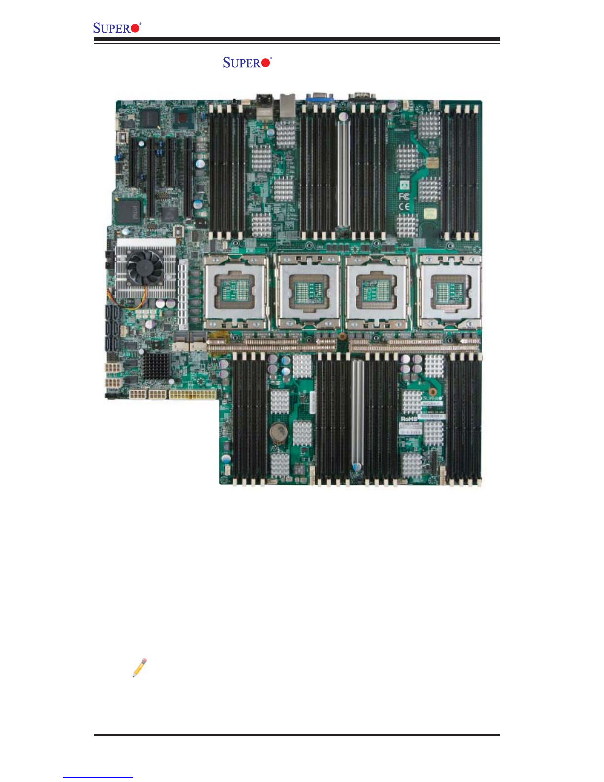
Motherboard Image
Note: All graphics shown in this manual were based upon the latest PCB
Revision available at the time of publishing of the manual. The motherboard
you've received may or may not look exactly the same as the graphics
shown in this manual.
2-2
Page 15
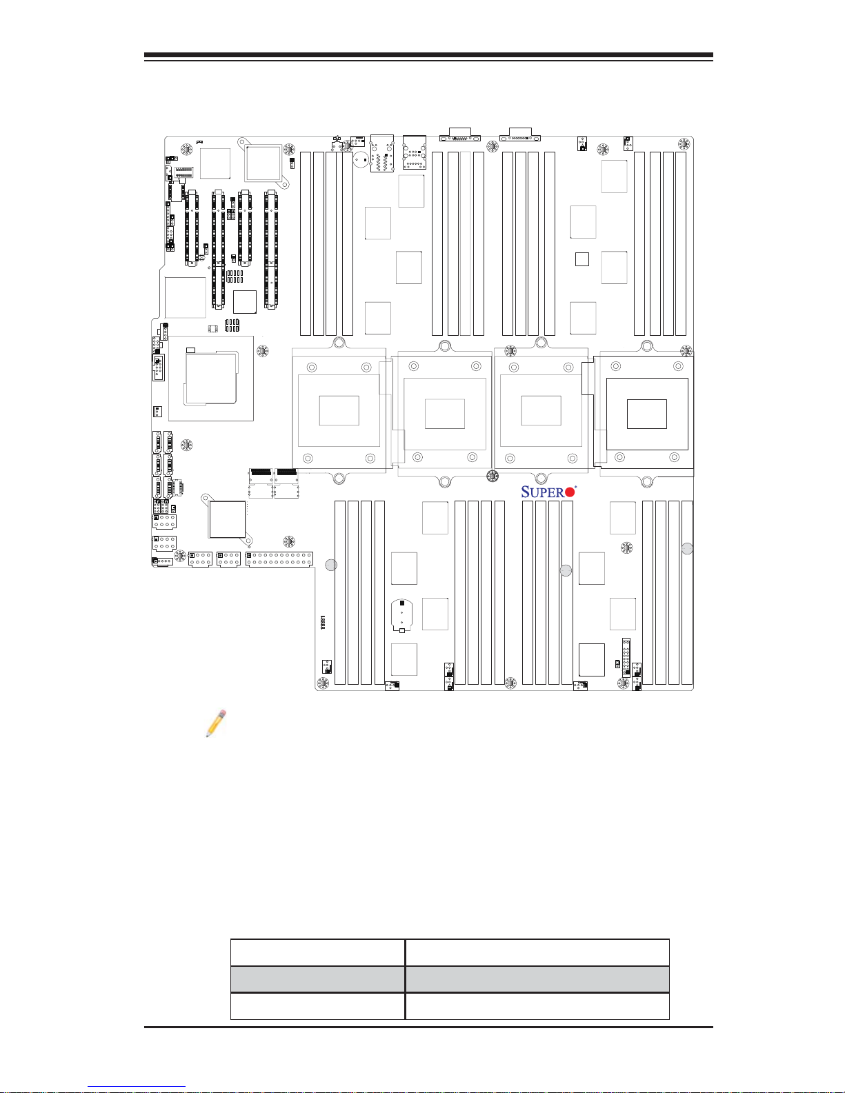
5
USB2/3
COM2
I-SATA0
I-SATA2
I-SATA4
JP6
JPWR4
JWOR
J40
JP4
J35
USB5
FAN 11
I-SATA5
JP5
JPWR5
JPRST1
D10
IPMB
BMCRST
U101
Slot1 PCI-E 2.0 X8
JD1
JWD1
JLPC1
JP10
JPB1
PORT80
1
JBT1
Intel ICH 10R
Intel
IOH 7500
I-SATA1
I-SATA3
J59
BBU
JL1
JPI2C1
BMC_HB
Winbond
BMC CTRL
JPS1
Slot2 PCI-E 2.0 X16/X8
JPT1
JPG1
JUID_OW1
U70
JP1
BIOS
LSI 2108
SAS CTRL
JPWR1JPWR2
Intel 82576
LAN CTRL
Slot3 PCI-E 2.0 X8
JP3
SAS0~3
JPWR3
UID_LED
JUIDB1
UID_SWITCH
JPL1
Slot4 PCI-E 2.0 X16/X8
P1-DIMM3A
P1-DIMM4A
SAS4~7
Motherboard Layout
USB0/1
FAN10
SP1
P1-DIMM1A
LAN1
(LOWER)
LAN2
(UPPER)
IPMI_LAN
P1-DIMM5A
LED26
P1-DIMM2A
CPU1
CPU2
VGA
P1-DIMM6A
P1-DIMM7A
P1-DIMM8A
COM1
P3-DIMM4A
P3-DIMM3A
P3-DIMM1A
P3-DIMM2A
CPU3
Chapter 2: Overview
FAN9
X8QBE-F
Rev. 1.11
FAN8
P3-DIMM6A
P3-DIMM5A
CPU4
P3-DIMM8A
P3-DIMM7A
P2-DIMM6A
P2-DIMM5A
LED5
LED7
LED8
P5V_STBY
LED9
LED6
FAN7
P2-DIMM7A
P2-DIMM8A
BT2
Battery
FAN6
P2-DIMM2A
P2-DIMM1A
P2-DIMM4A
P2-DIMM3A
FAN4
FAN
P4-DIMM8A
P4-DIMM7A
P4-DIMM6A
P4-DIMM5A
FAN3
JF1
OHLED
JOH1
FAN1
FAN2
P4-DIMM1A
P4-DIMM2A
P4-DIMM4A
P4-DIMM3A
Note 1: SAS2 connections and the LSI 2108 SAS2 Controller are available
on the X8QB6-F only. To enable battery backup support for onboard SAS,
an optional SAS Battery Backup Accessory kit is required. Refer to Page
3-26 in Chapter 3 for more details.
Note 2: For the latest CPU/Memory updates, please refer to our website
at http://www.supermicro.com/products/motherboard/ for details.
Note 3: To ensure adequate power supply to the motherboard for proper
system operation, please use a power supply that supports the following
specifi cations:
Type Minimum Requirement
12V 1400 Watts (minimum)
5V Standby 6A (minimum)
2-3
Page 16
5
USB2/3
COM2
I-SATA0
I-SATA2
I-SATA4
JP6
JPWR4
JWOR
J40
JP4
J35
FAN 11
I-SATA5
JP5
JPWR5
X8QB6-F/X8QBE-F Motherboard User’s Manual
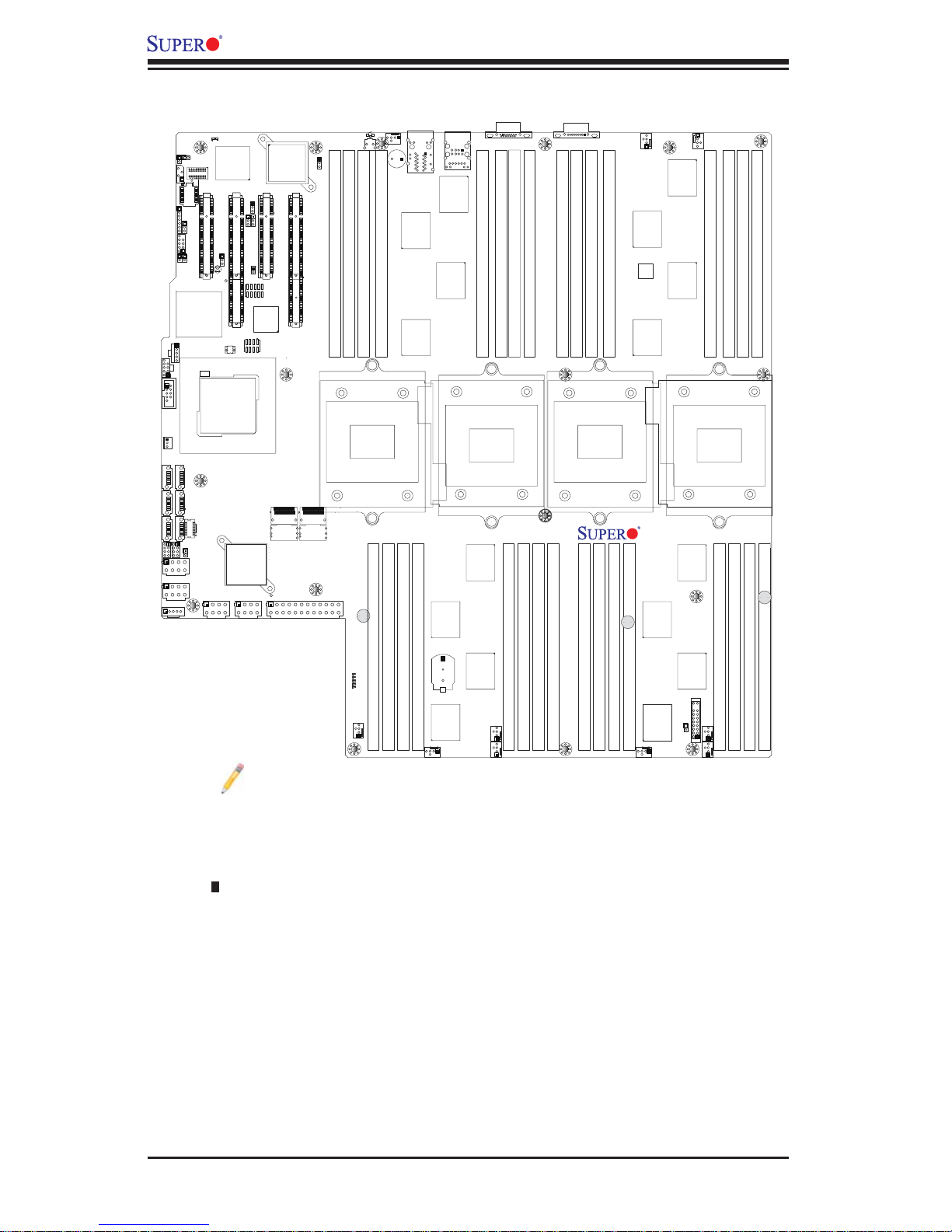
X8QB6-F/X8QBE-F Quick Reference
USB0/1
JPRST1
D10
IPMB
BMCRST
U101
JD1
JWD1
JLPC1
JP10
PORT80
1
Intel ICH 10R
USB5
I-SATA1
I-SATA3
J59
BBU
JL1
JPI2C1
BMC_HB
Winbond
BMC CTRL
JPS1
Slot2 PCI-E 2.0 X16/X8
Slot1 PCI-E 2.0 X8
JPT1
JPG1
JUID_OW1
JPB1
JBT1
U70
BIOS
Intel
IOH 7500
LSI 2108
SAS CTRL
JPWR1JPWR2
Intel 82576
LAN CTRL
Slot3 PCI-E 2.0 X8
JP3
JP1
SAS0~3
JPWR3
UID_LED
JUIDB1
UID_SWITCH
JPL1
Slot4 PCI-E 2.0 X16/X8
P1-DIMM3A
P1-DIMM4A
SAS4~7
LED26
P1-DIMM2A
CPU1
FAN10
SP1
P1-DIMM1A
LAN1
(LOWER)
LAN2
(UPPER)
IPMI_LAN
P1-DIMM5A
CPU2
VGA
P1-DIMM6A
P1-DIMM7A
P1-DIMM8A
COM1
P3-DIMM4A
P3-DIMM3A
P3-DIMM2A
P3-DIMM1A
CPU3
FAN9
X8QBE-F
Rev. 1.11
FAN8
P3-DIMM6A
P3-DIMM5A
CPU4
P3-DIMM8A
P3-DIMM7A
P2-DIMM6A
P2-DIMM5A
LED5
LED7
LED8
P5V_STBY
LED9
LED6
FAN7
P2-DIMM7A
P2-DIMM8A
BT2
Battery
FAN6
FAN4
FAN
P2-DIMM2A
P2-DIMM1A
P2-DIMM4A
P2-DIMM3A
P4-DIMM8A
P4-DIMM7A
P4-DIMM6A
P4-DIMM5A
FAN3
JF1
OHLED
JOH1
P4-DIMM1A
FAN1
FAN2
Notes:
See Chapter 3 for detailed information on jumpers, I/O ports and JF1 front
•
panel connections.
" " indicates the location of "Pin 1".
•
Jumpers not indicated are for testing only. •
The LSI SAS2 Controller and SAS2 Connections are available on the X8QB6-F •
only.
LED Indicators that are not documented are for testing only.
•
P4-DIMM3A
P4-DIMM2A
P4-DIMM4A
Use only the correct type of onboard CMOS battery as specifi ed by the •
manufacturer. Do not install the onboard battery upside down to avoid possible
explosion.
2-4
Page 17

Chapter 2: Overview
X8QB6-F/X8QBE-F Jumpers
Jumper
JBT1
Description Default Setting
Clear CMOS See Chapter 3
JPB1 BMC Enabled Pins 1-2 (Enabled)
JPG1 VGA Enabled Pins 1-2 (Enabled)
JPL1 GLAN1/GLAN2 Enable Pins 1-2 (Enabled)
JPRST1 BMC Reset Off (Normal)
JPS1 (X8QB6-F only) SAS2 Enabled Pins 1-2 (Enabled)
JPT1 TPM Enabled Pins 1-2 (Enabled)
JWD1 Watch Dog Pins 1-2 (Reset)
X8QB6-F/X8QBE-F Connectors
Connectors Description
BT2 Onboard Battery (See Chpt. 4 for Used Battery Disposal)
COM1/COM2 Backplane COM Port1/Front Accessible COM2 Header
FAN1~11 CPU/System Fan Headers (Fan1~Fan10)
(Fan11: Reserved)
IPMB 4-pin External BMC I
2
C Header (for an IPMI Card)
I-SATA 0~5 Intel SB SATA Connectors 0~5
J59 (BBU) (X8QB6-
F only)
LSI SAS Battery Backup Unit (BBU) (See Note on Pg.2-6,
3-26)
JD1 Speaker/Power LED Indicator
JF1 Front Panel Control Header
JL1 Chassis Intrusion
JLPC1 LPC Port 80
JOH1 Overheat/Fan Fail LED
2
JPI
C1 Power Supply SMBbus I2C Header
JPWR1~2,
12V 8-Pin Power Connectors (See Warning on Pg. 2-6.)
JPWR4~5
JPWR3 ATX 24-Pin Power Connector (See Warning on Pg. 2-6.)
JUID_OW1 UID Override Header
JWOR Wake-On-Ring Header
LAN1/LAN2 G-bit Ethernet Ports 1/2
(IPMI) LAN IPMI_Dedicated LAN
SAS 0~3, 4~7 Serial_Attached_SCSI Connectors 0~3, 4~7 (X8QB6-F)
SP1 Onboard Buzzer (Internal Speaker)
Slot1, Slot3 PCI-Express 2.0 x8
Slot2, Slot4 PCI-Express 2.0 x16/x8
2-5
Page 18
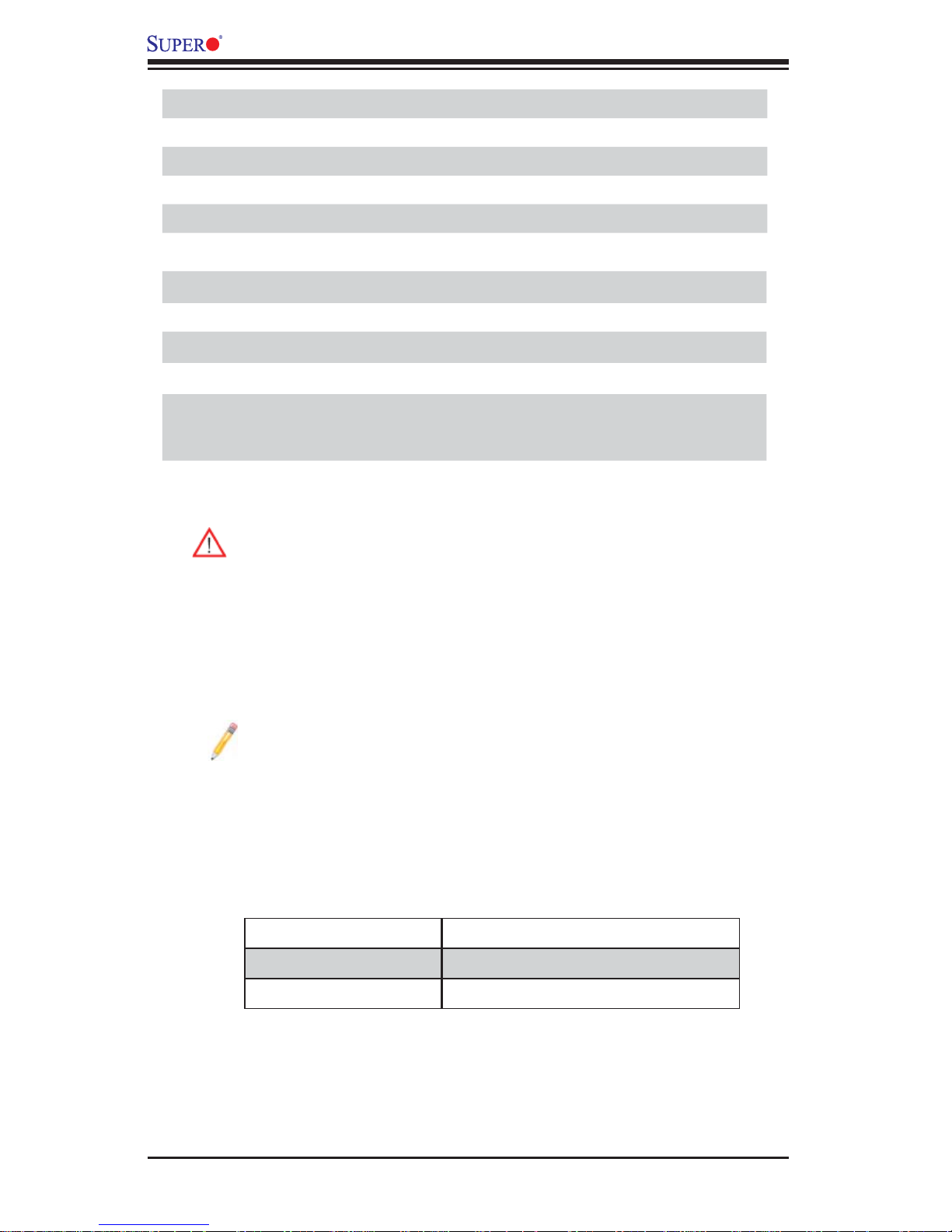
X8QB6-F/X8QBE-F Motherboard User’s Manual
T-SGPIO 1/2 Serial_Link General Purpose I/O Headers
BP USB 0/1 Back Panel USB 0/1
USB 2/3, USB 5 Front Panel Accessible USB Connections
UID Switch UID (Unit Identifi er) Switch
VGA Backpanel VGA Port
X8QB6-F/X8QBE-F LED Indicators
LED Description State Status
D10 BMC Heartbeat LED Green: Blinking Normal
LED 8 Stand by PWR LED Green: On SB Power On
LED 26 UI D LED
Warning!
To prevent damage to the power supply or motherboard, please use a power
•
supply that contains a 24-pin and at least three 8-pin power connectors. Be
sure to connect these power supply connectors to the 24-pin power connector
(JPWR3) and three of the 8-pin power connectors (JPWR1, JPWR2, JPWR4
or JPWR5) on the motherboard. Failure in doing so will void the manufacturer
warranty on your power supply and motherboard.
Note 1: To enable extended battery backup support for onboard SAS,
please purchase a LSI 2108 SAS Battery Accessory kit from Supermicro.
Refer to Page 3-26 in Chapter 3 for more details.
Note 2: To ensure adequate power supply to the motherboard for proper
system operation, please use a power supply that supports the following
specifi cations:
Blue: On (Windows OS),
Blinking (Linux)
Unit Identifi ed
Type Minimum Requirement
12V 1400 Watts (minimum)
5V Standby 6A (minimum)
2-6
Page 19

Motherboard Features
Chapter 2: Overview
CPU
Memory
Four Intel•
cessors; each processor supports four full-width Intel
QuickPath Interconnect (QPI) links (with support of
up to 25.6 GT/s per QPI link and with Data Transfer
Rate of up to 6.4 GT/s per direction)
Integrated memory controller supports:•
32 240-pin DDR3-1066 RDIMMs running at speeds 1.
of 1066/978/800 MHz (via an onboard buffer)
Support for up to 512 GB of Registered ECC 2.
DDR3 memory in two-channel memory bus
DIMM sizes
RDIMM
• 1GB, 2GB, 4GB, 8GB and 16GB
Virtualization: VT-x, VT-d, and VT-c
•
®
7500 Series (Socket LS-LGA 1567) pro-
Note: For the latest CPU/memory updates,
please refer to our website at http://www.supermicro.com/products/motherboard.
Chipset
Expansion
Slots
Graphics
Network
I/O: Intel® QuickData Technology with Intel 82576 •
LAN Controller, supports:
Intel 825761.
LSI 2108 (Hardware RAID w/Battery Backup)2.
Intel® 7500 Chipset (7500 IOH & ICH10R)•
Two (2) PCI Express 2.0 x16 slots (Slot2/Slot4),•
Two (2) PCI Express 2.0 x8 slots (Slot1/Slot3), or•
Four (4) PCI Express 2.0x8 slots (Slot1~Slot4)•
Winbond BMC Video Controller (Matrox G200eW)•
One Intel 82576 Gigabit (10/100/1000 Mb/s) Ethernet •
Dual-Channel Controller for LAN 1/LAN 2 ports.
Winbond WP450R Base-board Controller (BMC)
•
supports IPMI_LAN 2.0
2-7
Page 20
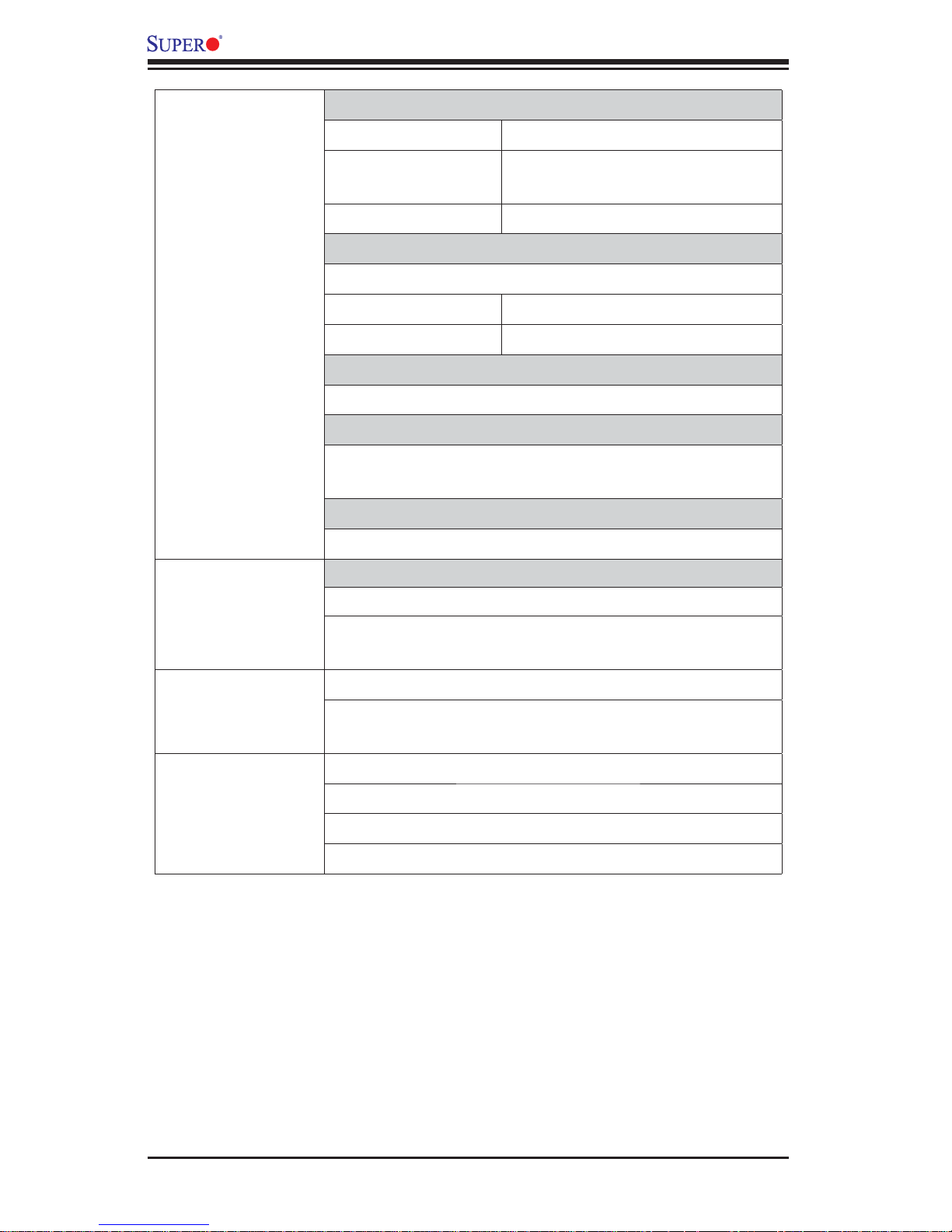
X8QB6-F/X8QBE-F Motherboard User’s Manual
I/O Devices
SATA Connections
SATA Ports
• Six (6)
RAID (Win-
•
dows)
RAID (Linux)
• RAID 0, 1, 10
SAS2 Connections
LSI SAS2 2108 Controller
•
SAS2 Ports• 0~3, 4~7
RAID Support
• RAID 0, 1, 5, 6, 10, 50, 60
Integrated IPMI 2.0
IPMI 2.0 supported by the WPCM450R BMC
•
Serial (COM) Port
One (1) Fast UART 16550 Connection: 9-pin RS-
•
232 port
Super I/O
Winbond Super I/O 83527
•
RAID 0, 1, 5, 10
Peripheral
Devices
BIOS
Power
Confi g.
USB Devices
Two (2) USB ports on the rear I/O panel (USB 0/1)
•
Three (3) USB connection for front access (USB •
2/3, USB 5)
64 Mb SPI AMI BIOS•
APM 1.2, PCI 2.3, ACPI 1.0/2.0/3.0, USB Keyboard,
•
Plug & Play (PnP) and SMBIOS 2.5
ACPI/ACPM Power Management•
Main switch override mechanism•
Keyboard Wake-up from Soft-Off•
Power-on mode for AC power recovery•
®
SM Flash BIOS
2-8
Page 21
Chapter 2: Overview
PC Health
Monitoring
System
Management
CPU Monitoring
Onboard voltage monitors for CPU1 Vcore, CPU2 •
Vcore, CPU3 Vcore, CPU4 Vcore, NIC Vcore, BMC
Vcore, AUX Vcore, Standby ME Vcore, 12V Scale,
1.5V, 3.3V Vcc(V), 3.3VSB, Battery Voltage, and
IOPV12.
•
CPU 7-Phase switching voltage regulator
CPU/System overheat LED and control•
CPU Thermal Trip support•
Thermal Monitor 2 (TM2) support•
Fan Control
Fan status monitoring with fi rmware 4-pin (Pulse
•
Width Modulation) fan speed control
Low noise fan speed control
•
PECI (Platform Environment Confi guration Interface) •
2.0 support
System resource alert via Supero Doctor III
•
SuperoDoctor III, Watch Dog, NMI•
Chassis Intrusion Header and Detection•
Dimensions
Note: For IPMI Confi guration Instructions, please refer to the Embedded
IPMI Confi guration User's Guide available @ http://www.supermicro.com/
support/manuals/.
16.79" (L) x 16.00" (W) (426.46 mm x 406.40 mm)•
2-9
Page 22
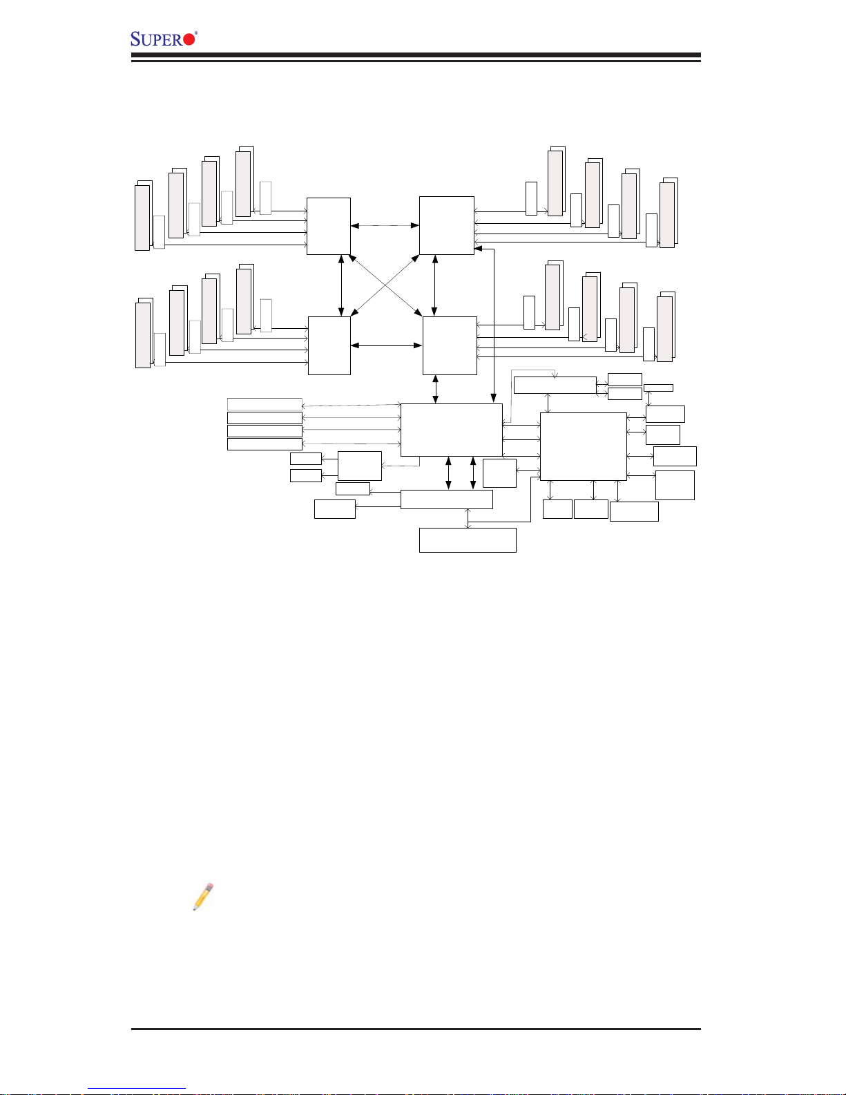
X8QB6-F/X8QBE-F Motherboard User’s Manual
(x2)
DDR3 800/1066
DDR3 800/1066
Mill Brook
(x2)
Mill Brook
DDR3 800/1066
DDR3 800/1066
(x2)
(x2)
(x2)
DDR3 800/1066
Mill Brook
(x2)
DDR3 800/1066
Mill Brook
(x2)
SMI
6.4GT/s
DDR3 800/1066
Mill Brook
SMI 6.4GT/s
Mill Brook
SMI 6.4GT/s
SMI 6.4GT/s
(x2)
SMI
6.4GT/s
DDR3 800/1066
Mill Brook
SMI 6.4GT/s
Mill Brook
SMI 6.4GT/s
SMI 6.4GT/s
Slot2 PCIE-G2x8
Slot3 PCIE-G2x16
Slot5 PCIE-G2x8
Slot6 PCIE-G2x16
SAS x4
SAS x4
FBD0
FBD1
FBD2
FBD3
FBD0
FBD1
FBD2
FBD3
PCIE-G2x8
PCIE-G2x8x2
PCIE-G2x8
PCIE-G2x8x2
USB
Ports x4
P
I
6
Q
Q
Processor 4
P
I
6
.
4
G
T
/
QPI 6.4GT/s
QPI 6.4GT/s
Processor 3
LSI 2018
SAS CTRL
BIOS
SPI
USB 2.0
Processor 2
T
/
s
.
4
G
s
/
T
G
4
.
s
6
I
P
Q
QPI 6.4GT/s
Processor 1
QPI 6.4GT/s
QPI#0 QPI#1
Intel 7500
IOH#1
Link
ICH10
SIO W83527HG
FBD0
FBD1
FBD2
FBD3
FBD0
FBD1
FBD2
FBD3
PCIE
LPC
6.4GT/s
SMI
SMI
SMI
QPI 6.4GT/s
SMI
6.4GT/s
SMI
SMI
SMI
Reset,
PWR,
GPIO
SMI
6.4GT/s
6.4GT/s
6.4GT/s
6.4GT/s
6.4GT/s
6.4GT/s
PCIE1.0x4
PCI
USB 1.0
USB 2.0
CTRL
LPC
(x2)
DDR3 800/1066
Mill Brook
Mill Brook
Kawela Dual GLAN
Mill Brook
(x2)
DDR3 800/1066
Mill Brook
RMII PHY
WPCM450R
Winbond BMC
(w/Video, KVM,
SIO, Fan Speed
CTRL, PECI,
Voltage Monitoring)
Fan CTRL
Serial
Fans
(x10)
Port
DDR3 800/1066
DDR3 800/1066
(x2)
(x2)
(x2)
DDR3 800/1066
Mill Brook
(x2)
DDR3 800/1066
Mill Brook
GLAN
GLAN
RMII
DDR2
SPI
SMBus
HM
W83795G
(x2)
DDR3 800/1066
Mill Brook
(x2)
DDR3 800/1066
Mill Brook
RJ45
10/100LAN
PHY
10/100
Rear
Video
Video
Memory
BMC
FW
Flash
Note: This is a general block diagram and may not exactly represent the
features on your motherboard. See the Motherboard Features pages for
the actual specifi cations of each motherboard.
System Block Diagram
2-10
Page 23

Chapter 2: Overview
2-2 Chipset Overview
Built upon the functionality and the capability of the Intel 7500 platform, the
X8QB6-F/X8QBE-F motherboard provides the performance and support for
quad_processor-based HPC/Cluster/Database servers. The 7500 platform consists of t he 7500 Seri es Socket-L S (LGA 1567) pro cessor, the 7500 (I OH), and
the ICH10 R (South Bridge).
With the Intel QuickPath interconnect (QPI) controller built in, the 7500 Series
processor offer s point-to-point system interconnect interface, enhancing system
performance by utilizing serial link interconnections with increased bandwidth
and scalability.
The 7500 IO Hub provides the interface between QPI-based processor, and
industr y-standard PCI- Express components. Each processor suppor ts four fullwidth, bi direc tional in terconn ects t hat run at the s peed of 4.8 GT/s, 5.8 6 GT/s or
6.4 GT/s. Each QPI link consists of 20 pairs of unidirectional differential lanes for
data tr ansmissi on in additio n to a diffe rential for warded c lock. Th e two x16 PCI
Expr ess G en 2 co nnect ions c an al so be c onfi gured as x 8 and x4 link s to com ply
with PCI-E Base Specifi cati on, Rev. 2.0. The se PC I - E G en 2 l ane s sup po r t p eer-
to-peer read and write transa ctions. In add i t ion, the legac y I OH provides a x4 ESI
(Enterpr ise Sou th Bri dge Inter f ace) link suppor t fo r the leg acy br idge.
The 7500 chipset also offers a wide range of ESI, Intel® I/OAT Gen 3, Intel
VT-d an d RAS (Reliabi lity, Availabili ty and Ser viceabilit y) suppor t. The feature s
suppor ted includ e memory inte rface ECC, x4/ x8 Single Devic e Data Cor rection
(SDDC), Flow-through CRC (Cyclic Redundancy Check), parity protection, outof-ba nd registe r acces s via SM Bus, memo ry mir rorin g, and Hot- plug supp ort o n
the PCI - Expr ess Inter f ace.
Main Features of the 7500 Platform
Fully-connectivity (with four Intel® QuickPath Interconnects and up to eight cores •
in each socket with 24MB of shared last level (L3) cache supported)
CPU-Integrated memory controller with support of DDR-3 1066 MHz RDIMMS
•
running at 800/978/1066 MHz via a memory buffer
Virtualization Technology, Integrated Manageability Engine (ME) supported
•
44 bits physical address and 48 bits virtual address supported•
2-11
Page 24

X8QB6-F/X8QBE-F Motherboard User’s Manual
2-3 Special Features
Recovery from AC Power Loss
The Basic I/O System (BIOS) provides a setting for you to determine how the system will respond when AC power is lost and then restored to the system. You can
choose for the system to remain powered off (in which case you must press the
power switch to turn it back on), or for it to automatically return to the power- on
state. See the Advanced BIOS Setup section for this setting. The default setting
is Last State.
2-4 PC Health Monitoring
This section describes the PC health monitoring features of the motherboard. This
motherboard has an onboard System_Hardware_Monitor chip that supports PC
health monitoring. An onboard voltage monitor will scan the following onboard voltages continuously: CPU1 Vcore, CPU2 Vcore, CPU3 Vcore, CPU4 Vcore, +1.0V,
+1.2V, +1.8V, +1.1V, +12V, 1.5V, 3.3V V, 3.3VSB, Battery Voltage, and IOPV12.
Once a voltage becomes unstable, a warning is given or an error message is sent
to the screen. The user can adjust the voltage thresholds to defi ne the sensitivity
of the voltage monitor.
Fan Status Monitor with Firmware Control
The PC health monitor can check the RPM status of the cooling fans. The onboard
CPU and chassis fans are controlled by BIOS Thermal Management (under the
Hardware Monitoring section in the Advanced Setting).
Environmental Temperature Control
A thermal control sensor monitors the CPU temperature in real time and will turn
on the thermal control fan whenever the CPU temperature exceeds a user-defi ned
threshold. The overheat circuitry runs independently from the CPU. Once it detects
that the CPU temperature is too high, it will automatically turn on the thermal fan
control to prevent the CPU from overheating. The onboard chassis thermal circuitry
can monitor the overall system temperature and alert the user when the chassis
temperature is too high.
Note: To avoid possible system overheating, please be sure to provide
adequate airfl ow to your system.
2-12
Page 25

Chapter 2: Overview
System Resource Alert
This feature is available when used with Supero Doctor III in the Windows OS
environment or used with Supero Doctor II in Linux. Supero Doctor is used to notify
the user of certain system events. For example, you can confi gure Supero Doctor
to provide yo u with warn ings when th e system temper ature, CPU tempe ratures,
voltag es and fa n speed s go beyond a p redefi ned range.
2-5 ACPI Features
ACPI stands for Advanced Confi guration and Power Interface. The ACPI specifi ca-
tion defi nes a fl exible and abstract hardware interface that provides a standard
way to integrate power management features throughout a PC system, including
its hardware, operating system and application software. This enables the system
to automatically turn on and off peripherals such as CD-ROMs, network cards, hard
disk drives and printers.
In addition to enabling operating system-directed power management, ACPI also
provides a generic system event mechanism for Plug and Play, and an operating
system-independent interface for confi guration control. ACPI leverages the Plug and
Play BIOS data structures, while providing a processor architecture-independent
implementation that is compatible with Windows XP, Windows Vista and Windows
2008 Operating Systems.
Slow Blinking LED for Suspend-State Indicator
When the CPU goes into a suspend state, the chassis power LED will start blinking
to indicate that the CPU is in suspend mode. When the user presses any key, the
CPU will "wake up" and the LED will automatically stop blinking and remain on.
2-6 Power Supply
As with all computer products, a stable power source is necessary for proper and
reliable operation. It is even more important for processors that have high CPU
clock rates.
The X8QB6-F/X8QBE-F motherboard accommodates 24-pin ATX power supplies.
Although most power supplies generally meet the specifi cations required by the
CPU, some are inadequate. In addition, four 12V 8-pin power connections are
also required to ensure adequate power supply to the system. Also, be sure to
use a power supply that supports the specifi cations listed in the table on Page
2-3 or 2-6.
Warning! To prevent damage to the power supply or motherboard, please
use a power supply that contains a 24-pin and at least three 8-pin power
2-13
Page 26

X8QB6-F/X8QBE-F Motherboard User’s Manual
connectors. Be sure to connect these power supply connectors to the
24-pin (JPWR3) and three of the four 8-pin power connectors (JPWR1,
JPWR2, JPWR4, or JPWR5) on the motherboard. Failure to do so will void
the manufacturer warranty on your power supply and motherboard.
It is strongly recommended that you use a high quality power supply that meets ATX
power supply Specifi cation 2.02 or above. It must also be SSI compliant. (For more
information, please refer to the website at http://www.ssiforum.org/). Additionally, in
areas where noisy power transmission is present, you may choose to install a line
fi lter to shield the computer from noise. It is recommended that you also install a
power surge protector to help avoid problems caused by power surges.
2-7 Super I/O
The Super I/O supports two high-speed, 16550 compatible serial communication
ports (UARTs). Each UART includes a 16-byte send/receive FIFO, a programmable
baud rate generator, complete modem control capability and a processor interrupt
system. Both UARTs provide legacy speed with baud rate of up to 115.2 Kbps
as well as an advanced speed with baud rates of 250 K, 500 K, or 1 Mb/s, which
support higher speed modems.
The Super I/O provides functions that comply with ACPI (Advanced Confi guration
and Power Interface), which includes support of legacy and ACPI power management through an SMI or SCI function pin. It also features auto power management
to reduce power consumption.
2-8 Overview of the Nuvoton WPCM450R Controller
The Nuvoton WPCM450R Controller is a Baseboard Management Controller
(BMC) that supports the PCI-compatible 2D/VGA Graphics Core, Virtual Media,
and Keyboard/Video/Mouse Redirection (KVMR) modules. With blade-oriented
Super I/O capability built-in, the WPCM450R Controller is ideal for legacy-reduced
server platforms.
The WPCM450R interfaces with the host system via a PCI interface to communicate with the Graphics core. It supports USB 2.0 and 1.1 for remote keyboard/
mouse/virtual media emulation. It also provides LPC interface to control Super IO
functions. The WPCM450R is connected to the network via an external Ethernet
PHY module.
The WPCM450R communicates with onboard components via six SMBus interfaces, fan control, and Platform Environment Control Interface (PECI) buses.
Note: For more information on IPMI confi guration, please refer to the
Embedded IPMI User's Guide posted on our website @ http://www.supermicro.com/support/manuals/.
2-14
Page 27

Chapter 3: Installation
Chapter 3
Installation
3-1 Static-Sensitive Devices
Electrostatic Discharge (ESD) can damage electronic com ponents. To avoid damaging your system board, it is important to handle it very carefully. The following
measures are generally suffi cient to protect your equipment from ESD.
Precautions
Use a grounded wrist strap designed to prevent static discharge.•
Touch a grounded metal object before removing the board from the antistatic •
bag.
Handle the board by its edges only; do not touch its components, peripheral
•
chips, memory modules or gold contacts.
When handling chips or modules, avoid touching their pins.
•
Put the motherboard and peripherals back into their antistatic bags when not •
in use.
For grounding purposes, make sure that your system chassis provides excellent
•
conductivity between the power supply, the case, the mounting fasteners and
the motherboard.
Unpacking
The motherboard is shipped in antistatic packaging to avoid static damage. When
unpacking the board, make sure that the person handling it is static protected.
3-1
Page 28
X8QB6-F/X8QBE-F Motherboard User's Manual
!
3-2 Processor and Heatsink Installation
When handling the processor package, avoid placing direct pressure on
the label area of the fan.
Notes:
Always connect the power cord last, and always remove it before adding, 1.
removing or changing any hardware components. Make sure that you install
the processor into the CPU socket before you install the CPU heatsink.
Make sure to install the motherboard into the chassis before you install the 2.
CPU heatsink and heatsink fans.
When purchasing a motherboard without a 7500 Series processor pre-3.
installed, make sure that the CPU socket plastic cap is in place, and none of
the CPU socket pins are bent; otherwise, contact the retailer immediately.
Refer to the M other boar d Features S ecti on of the m anual and o ur websit e 4.
for more d etails o n CPU supp or t and upd ates.
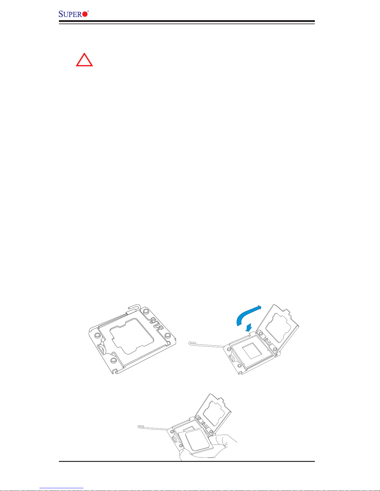
Installing an LGA 1567 Processor
Press the socket clip to release the load plate, which covers the CPU socket, 1.
from its locking position.
Gently lift the socket clip to open the load plate.2.
Hold the plastic cap at its north and south center edges to remove it from the 3.
CPU socket.
3-2
Page 29
Chapter 3: Installation
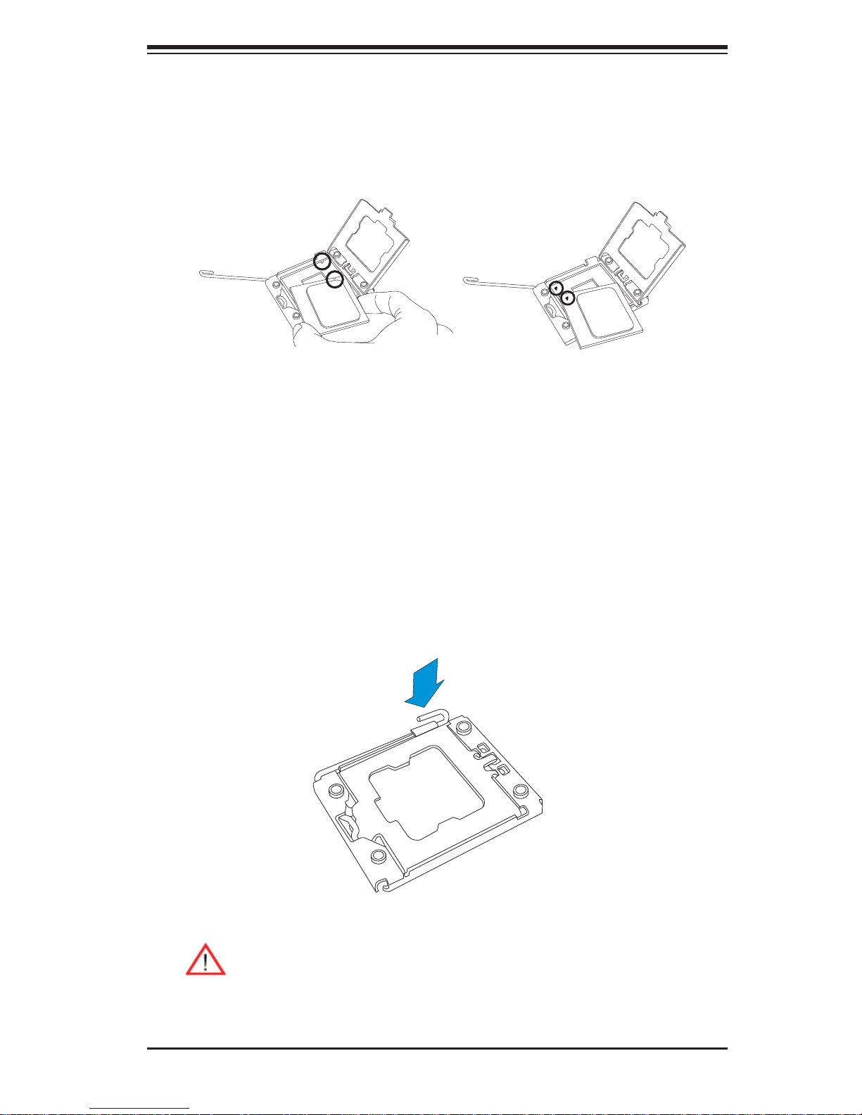
After removing the plastic cap, using your thumb and the index fi nger, hold 4.
the CPU at the north and south center edges.
Align the CPU key, which is a semi-circle cutout, against the socket key, 5.
which is the notch below the gold color dot on the side of the socket.
CPU Key
CPU Pin 1
Align Pin 1 on the CPU against Pin 1 on the CPU socket.6.
Once both CPU and the socket are aligned, carefully lower the CPU straight 7.
down into the socket. (To avoid damaging the CPU or the socket, do not rub
the CPU against the surface of the socket or its pins.)
With the CPU inside the socket, inspect the four corners of the CPU to make 8.
sure that the CPU is properly installed.
Once the CPU is securely seated on the socket, lower the CPU load plate to 9.
the socket.
Use your thumb to gently push the socket clip down to the clip lock.10.
Warning: Please save the plastic cap. The motherboard must be shipped
with the plastic cap properly installed to protect the CPU socket pins.
Shipment without the plastic cap properly installed will cause damage
to the socket pins.
3-3
Page 30
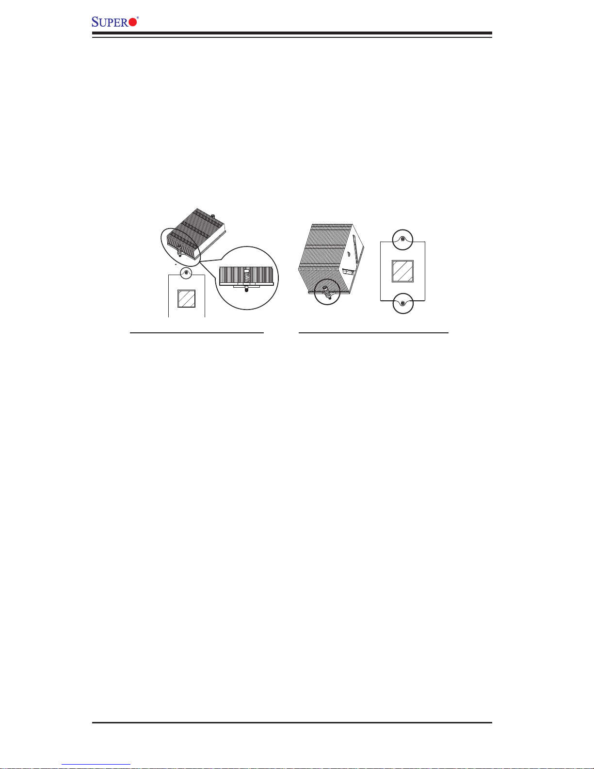
X8QB6-F/X8QBE-F Motherboard User's Manual
Installing a Passive CPU Heatsink
Apply the proper amount of thermal grease (with thickness of up to 0.13 mm) 1.
to the heatsink.
Place the heatsink on top of the CPU so that the two mounting holes on the 2.
heatsink are aligned with those on the retention mechanism.
3. Inser t t wo push -pin s on the s ides of t he heats ink thr ough th e mounti ng hol es
on the mot her board, a nd tur n the pus h- pins cl ock wis e to loc k them.
1U Heatsink (SNK-P0044P) 2U/4U Heatsink (SNK-P0045P)
3-4
Page 31
Chapter 3: Installation
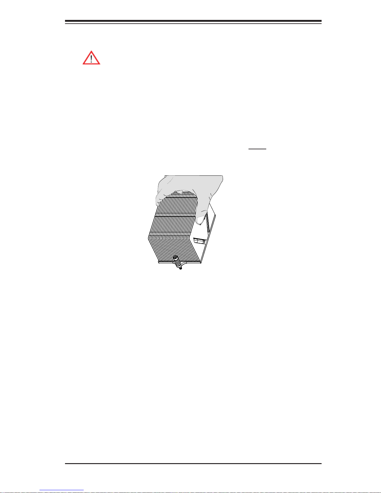
Removing the Passive Heatsink
Warni ng: We do not recommend that the CPU or the heatsink be re-
moved. However, if you do need to remove the heatsink, please follow
the instructions below to uninstall the heatsink to avoid damaging the
CPU or othe r comp onents.
Unplug the power cord from the power supply.1.
Press down the push-pin on the heatsink, and turn counter-clock-wise to 2.
loosen it. Repeat the same step to loosen the second push-pin.
Hold the heatsink as shown in the picture below, and 3. gently wriggle the heatsink to loosen it from the CPU. (Do not use excessive force when wriggling
the heatsink.)
Once the heatsink is loosened, remove the heatsink from the motherboard.4.
To reinstall the CPU and the heatsink, clean the surface of the CPU and the 5.
heatsink to get rid of the old thermal grease. Reapply the proper amount of
thermal grease on the surface before reinstalling them on the motherboard.
3-5
Page 32
X8QB6-F/X8QBE-F Motherboard User's Manual
5
3-3 Installing and Removing the Memory Modules
Note: Check Supe rmic ro's web site for r ecom mende d memo ry m odule s.
CAUTION
Exercise extreme care when installing or removing DIMM
module s to prevent a ny possi ble dam age.
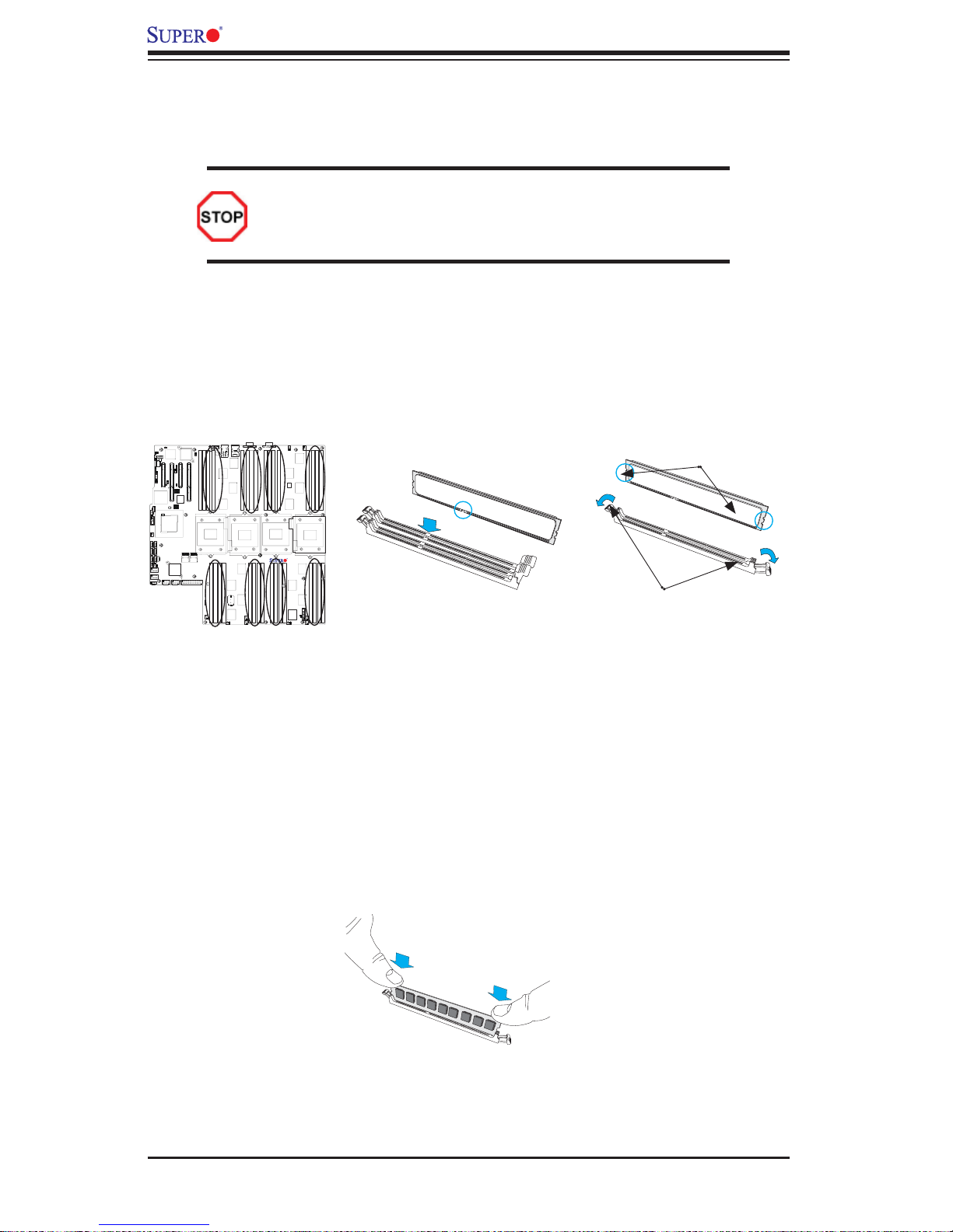
Installing & Removing DIMMs
Insert the desired number of DIMMs into the memory slots, starting with P1-1.
DIMM #1A. (For best performance, please use the memory modules of the
same type and speed in the same bank.)
Push the release tabs outwards on both ends of the DIMM slot to unlock it.2.
USB0/1
LAN1
COM1
VGA
LED26
BMC_HB
Slot2 PCI-E 2.0 X16/X8
JPT1
JUID_OW1
U70
BIOS
LSI 2108
SAS CTRL
JPWR1JPWR2
FAN10
UID_LED
(LOWER)
JUIDB1
UID_SWITCH
JPL1
Intel 82576
LAN CTRL
SP1
IPMI_LAN
LAN2
(UPPER)
JPS1
Slot4 PCI-E 2.0 X16/X8
Slot3 PCI-E 2.0 X8
JPG1
JP3
JP1
SAS0~3
SAS4~7
JPWR3
P1-DIMM5A
P1-DIMM1A
P1-DIMM6A
P1-DIMM3A
P1-DIMM4A
LED5
P5V_STBY
LED6
P1-DIMM7A
P1-DIMM2A
CPU1
CPU2
P2-DIMM6A
P2-DIMM5A
P2-DIMM7A
P2-DIMM2A
P2-DIMM8A
P2-DIMM1A
BT2
LED7
Battery
LED8
LED9
FAN7
FAN4
FAN
FAN6
FAN8
FAN9
P3-DIMM6A
P3-DIMM8A
P3-DIMM7A
P3-DIMM1A
P3-DIMM2A
P3-DIMM4A
P3-DIMM3A
P1-DIMM8A
P2-DIMM3A
P3-DIMM5A
CPU3
CPU4
X8QBE-F
Rev. 1.11
P4-DIMM4A
P4-DIMM6A
P2-DIMM4A
P4-DIMM3A
P4-DIMM8A
P4-DIMM1A
P4-DIMM2A
P4-DIMM5A
P4-DIMM7A
JF1
OHLED
FAN1
JOH1
FAN3
FAN2
Release Tabs
Notches
Align the key of the DIMM module with the receptive point on the memory 3.
slot.
JPRST1
JWOR
D10
IPMB
Winbond
BMCRST
J40
BMC CTRL
JP4
U101
Slot1 PCI-E 2.0 X8
JD1
JWD1
JLPC1
JP10
JPB1
PORT80
1
J35
JBT1
Intel ICH 10R
USB5
USB2/3
COM2
Intel
IOH 7500
FAN 11
I-SATA1
I-SATA0
I-SATA3
I-SATA2
I-SATA5
I-SATA4
J59
BBU
JP6
JP5
JL1
JPWR5
JPWR4
JPI2C1
Align the notches on both ends of the module against the receptive points on 4.
the ends of the slot.
Use two thumbs together to press the notches on both ends of the module 5.
straight down into the slot until the module snaps into place.
Press the release tabs to the lock positions to secure the DIMM module into 6.
the slot.
Press both notches straight down into
the memory slot at the same time.
Removing Memory Modules
Reverse the steps above to remove the DIMM
modules from the motherboard.
3-6
Page 33
Chapter 3: Installation
Memory Support for the X8QB6-F/X8QBE-F Motherboard
The X8QB6-F/X8QBE-F Motherboard supports up to 512 GB Registered ECC
DDR3 1066 MHz memory in 32 DIMM slots. These RDIMMs run at 800/978/1066
via a memory buffer. For the latest memory updates, please refer to our website a
at http://www.supermicro.com/products/motherboard.
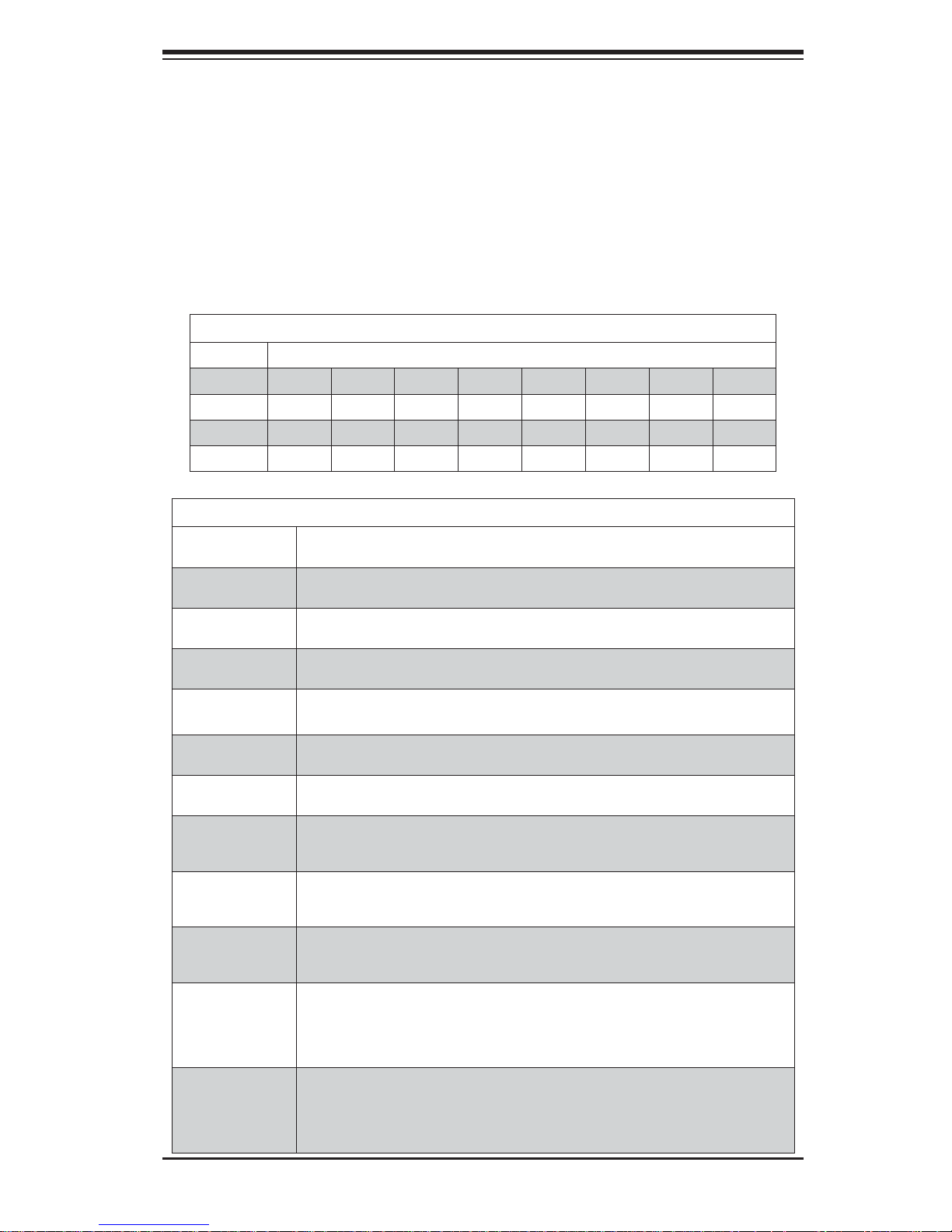
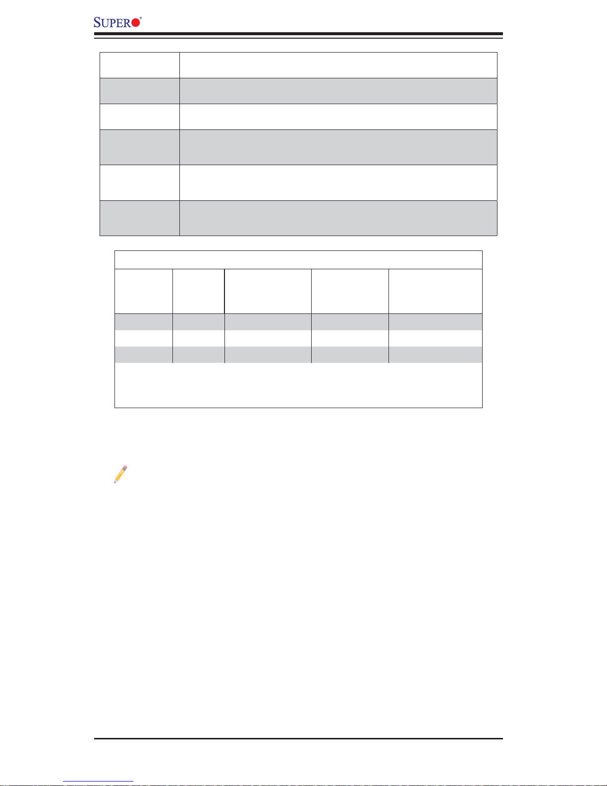
Processor & Memory Module Population Confi guration
For memor y to wor k pro perl y, follow the tab les be low for me mor y inst allati on.
Processors and their Corresponding Memory Modules
CPU# Corresponding DIMM Modules
CPU 1 P1-1A P1-2A P1-3A P1-4A P1-5A P1-6A P1-7A P1-8A
CPU2 P2-1A P2-2A P2-3A P2-4A P2-5A P2-6A P2-7A P2-8A
CPU3 P3-1A P3-2A P3-3A P3-4A P3-5A P3-6A P3-7A P3-8A
CPU4 P4-1A P4-2A P4-3A P4-4A P4-5A P4-6A P4-7A P4-8A
Number of
CPUs+DIMMs
1 CPU &
2 DIMMs
1 CPU &
4 DIMMs
1 CPU &
5~8 DIMMs
2 CPUs &
4 DIMMs
2 CPUs &
6 DIMMs
2 CPUs &
8 DIMMs
2 CPUs &
10~16 DIMMs
3 CPUs &
6 DIMMs
3 CPUs &
8 DIMMs
3 CPUs &
10 DIMMs
4 CPUs &
12 DIMMs
Processor and Memory Module Population
CPU and Memory Population Confi guration Table
(*For memory to work proper, please install DIMMs in pairs)
CPU1
P1-1A/P1-3A
CPU1
P1-1A/P1-3A, P1-5A/P1-7A
CPU1
P1-1A/P1-3A, P1-5A/P1-7A + Any memory pairs in P1-2A/-4A/-6A/-8A DIMM slots
CPU1 + CPU2
P1-1A/P1-3A, P2-1A/P2-3A
CPU1 + CPU2
P1-1A/P1-3A/P1-5A/P1-7A, P2-1A/P2-3A
CPU1 + CPU2
P1-1A/P1-3A/P1-5A/P1-7A, P2-1A/P2-3A/P2-5A/P2-7A
CPU1/CPU2
P1-1A/P1-3A/P1-5A/P1-7A, P2-1A/P2-3A/P2-5A/P2-7A + Any memory pairs in P1, P2
DIMM slots
CPU1/CPU2 + CPU3 or CPU4
P1-1A/P1-3A, P2-1A/P2-3A + P3-1A/P3-3A (if CPU 3 is installed)
P1-1A/P1-3A, P2-1A/P2-3A + P4-1A/P4-3A (if CPU 4 is installed)
CPU1/CPU2 + CPU3 or CPU4
P1-1A/P1-3A/P1-5A/P1-7A, P2-1A/P2-3A + P3-1A/P3-3A (if CPU 3 is installed)
P1-1A/P1-3A/P1-5A/P1-7A, P2-1A/P2-3A + P4-1A/P4-3A (if CPU 4 is installed)
CPU1/CPU2 + CPU3 or CPU4
P1-1A/P1-3A/P1-5A/P1-7A, P2-1A/P2-3A/P2-5A/P2-7A + P3-1A/P3-3A (if CPU 3 is
installed)
P1-1A/P1-3A/P1-5A/P1-7A, P2-1A/P2-3A/P2-5A/P2-7A + P4-1A/P4-3A (if CPU 4 is
installed)
CPU1/CPU2 + CPU3 or CPU4
P1-1A/P1-3A/P1-5A/P1-7A, P2-1A/P2-3A/P2-5A/P2-7A + P3-1A/P3-3A/ P3-5A/P3-7A
(if CPU 3 is installed)
P1-1A/P1-3A/P1-5A/P1-7A, P2-1A/P2-3A/P2-5A/P2-7A + P4-1A/P4-3A/ P4-5A/P43-7A
(if CPU 4 is installed)
3-7
Page 34
X8QB6-F/X8QBE-F Motherboard User's Manual
4 CPUs &
8 DIMMs
4 CPUs &
10 DIMMs
4 CPUs &
12 DIMMs
4 CPUs &
14 DIMMs
4 CPUs &
16 DIMMs
4 CPUs &
18~32 DIMMs
CPU1/CPU2/CPU3/CPU4
P1-1A/P1-3A, P2-1A/P2-3A,P3-1A/P3-3A + P4-1A/P4-3A
CPU1/CPU2/CPU3/CPU4
P1-1A/P1-3A/P1-5A/P1-7A, P2-1A/P2-3A,P3-1A/P3-3A + P4-1A/P4-3A
CPU1/CPU2/CPU3/CPU4
P1-1A/P1-3A/P1-5A/P1-7A, P2-1A/P2-3A/P2-5A/P2-7A, P3-1A/P3-3A, P4-1A/P4-3A
CPU1/CPU2/CPU3/CPU4
P1-1A/P1-3A/P1-5A/P1-7A, P2-1A/P2-3A/P2-5A/P2-7A,P3-1A/P3-3A/P3-5A/P3-7A,
P4-1A/P4-3A
CPU1/CPU2/CPU3/CPU4
P1-1A/P1-3A/P1-5A/P1-7A, P2-1A/P2-3A/P2-5A/P2-7A,P3-1A/P3-3A/P3-5A/P3-7A,
P4-1A/P4-3A/P4-5A/P4-7A
CPU1/CPU2/CPU3/CPU4
P1-1A/P1-3A/P1-5A/P1-7A, P2-1A/P2-3A/P2-5A/P2-7A,P3-1A/P3-3A/P3-5A/P3-7A,
P4-1A/P4-3A/P4-5A/P4-7A + any pairs in the other DIMM slots
RDIMM Support POR on the 7500 Series Processor Platform
DIMM Slots
per DDR
Channel
1 1 Reg. ECC DDR3 800,978, 1066 SR, DR, or QR
2 1 Reg. ECC DDR3 800,978, 1066 SR, DR, or QR
2 2 Reg. ECC DDR3 800,978, 1066 Mixing SR, DR, QR
Population Rules:
1. Any combination of x4 and x8 RDIMMs with 1 Gb or 2 Gb DRAM Density are supported.
2. Populate DIMMs starting with DIMM1A.
3. When mixing QR with SR or DR on the same DDR channel, put the QR in DIMM1A fi rst.
DIMMs
Populated
per DDR
Channel
RDIMM Type
(RDIMM: Reg.=
Registered)
POR Speeds (in
MHz)
Ranks per DIMM
(Any Combination)
Other Notes and Restrictions
Only DDR3 1066 RDIMMs are validated at speeds of 800, 978, 1066 MHz.•
For the memory modules to work properly, please install DIMM modules in pairs •
(w/even number of DIMMs installed).
All channels in a system will run at the fastest common frequency.
•
3-8
Page 35
Chapter 3: Installation
5
3-4 Motherboard Installation
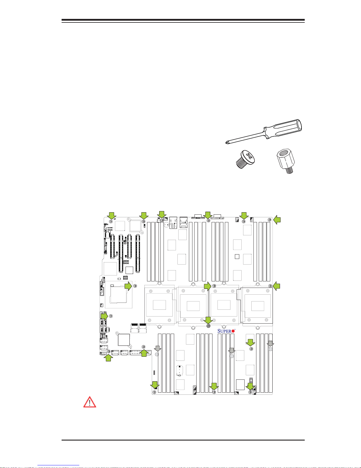
All motherboards have standard mounting holes to fi t different types of chassis.
Make sure that the locations of all the mounting holes for both motherboard and
chassis match. Although a chassis may have both plastic and metal mounting fasteners, metal ones are highly recommended because they ground the motherboard
to the chassis. Make sure that the metal standoffs click in or are screwed in tightly.
Then use a screwdriver to secure the motherboard onto the motherboard tray.
Tools Needed
Phillips Screwdriver•
Pan head screws (17 pieces)•
Standoffs (17 pieces)•
Additional Standoffs Holes marked with grey arrows •
(3 locations on the chassis, if needed)
Location of Mounting Holes
There are 17 mounting holes on this motherboard indicated by the arrows.
LED26
UID_LED
JUIDB1
UID_SWITCH
P1-DIMM3A
P1-DIMM4A
LED5
P5V_STBY
LED6
FAN7
P1-DIMM2A
CPU1
LED7
LED8
LED9
FAN10
P1-DIMM1A
P2-DIMM7A
P2-DIMM8A
USB2/3
COM2
I-SATA0
I-SATA2
I-SATA4
JP6
J40
FAN 11
I-SATA5
JPWR5
JPWR4
JPRST1
JWOR
IPMB
BMCRST
JP4
U101
JD1
JWD1
JLPC1
JP10
PORT80
1
J35
Intel ICH 10R
USB5
I-SATA1
I-SATA3
J59
JP5
JL1
JPI2C1
D10
JBT1
BBU
Winbond
BMC CTRL
Slot1 PCI-E 2.0 X8
JPB1
Intel
IOH 7500
BMC_HB
JPS1
Slot2 PCI-E 2.0 X16/X8
JPT1
JPG1
JUID_OW1
JP3
U70
JP1
BIOS
LSI 2108
SAS CTRL
JPWR1JPWR2
Intel 82576
LAN CTRL
Slot4 PCI-E 2.0 X16/X8
Slot3 PCI-E 2.0 X8
SAS0~3
SAS4~7
JPWR3
JPL1
Caution: 1) To avoid damaging the motherboard and its components,
please do not use a force greater than 8 lb/inch on each mounting screw
during motherboard installation. 2) Some components are very close to the
mounting holes. Please take precautionary measures to prevent damage
to these components when installing the motherboard to the chassis.
SP1
P2-DIMM6A
LAN1
(LOWER)
LAN2
(UPPER)
P2-DIMM5A
FAN6
BT2
Battery
USB0/1
IPMI_LAN
P1-DIMM5A
P1-DIMM6A
CPU2
FAN4
FAN
VGA
P1-DIMM7A
P2-DIMM1A
P1-DIMM8A
P2-DIMM2A
P2-DIMM3A
COM1
P3-DIMM4A
P2-DIMM4A
P3-DIMM2A
P3-DIMM3A
CPU3
P4-DIMM8A
P3-DIMM1A
P4-DIMM6A
P4-DIMM7A
FAN9
X8QBE-F
Rev. 1.11
P4-DIMM5A
FAN3
FAN8
JF1
OHLED
JOH1
P3-DIMM5A
CPU4
P4-DIMM1A
FAN1
FAN2
P3-DIMM6A
P3-DIMM7A
P4-DIMM2A
P3-DIMM8A
P4-DIMM4A
P4-DIMM3A
3-9
Page 36
X8QB6-F/X8QBE-F Motherboard User's Manual
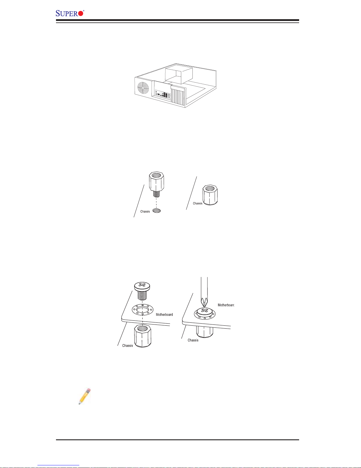
Installing the Motherboard
Install the I/O shield into the chassis. 1.
Locate the mounting holes on the motherboard. 2.
Locate the matching mounting holes on the chassis. Align the mounting holes 3.
on the motherboard against the mounting holes on the chassis.
Install standoffs in the chassis as needed.4.
Install the motherboard into the chassis carefully to avoid damaging mother-5.
board components.
Using the Philips screwdriver, insert a Pan head #6 screw into a mounting 6.
hole on the motherboard and its matching mounting hole on the chassis.
Repeat Step 5 to insert #6 screws into all mounting holes.7.
Make sure that the motherboard is securely placed in the chassis.8.
Note: Images displayed are is for illustration only. Your chassis or components might look different from those shown in this manual.
3-10
Page 37
Chapter 3: Installation
5
P4
DIMM4A
1
2
3
4
5
678
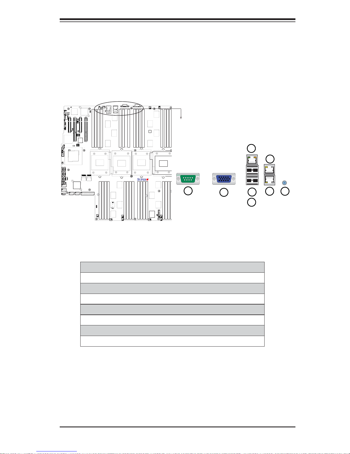
3-5 Control Panel Connectors/I/O Ports
The I/O p ort s are col or cod ed in co nforma nce wit h the PC 9 9 speci fi cation. See
the pic ture be low for t he co lors a nd loc atio ns of the var ious I /O por t s.
Back Panel Connectors/I/O Ports
USB0/1
LAN1
LED26
JPRST1
JWOR
BMC_HB
D10
Intel 82576
IPMB
Winbond
BMCRST
J40
BMC CTRL
U101
JD1
JWD1
JLPC1
JP10
PORT80
1
Intel ICH 10R
USB5
I-SATA1
I-SATA3
J59
JP5
JL1
JPI2C1
BBU
Slot2 PCI-E 2.0 X16/X8
Slot1 PCI-E 2.0 X8
JPB1
JBT1
U70
BIOS
Intel
IOH 7500
LSI 2108
SAS CTRL
JPWR1JPWR2
JPS1
JPT1
JUID_OW1
LAN CTRL
Slot3 PCI-E 2.0 X8
JPG1
JP3
JP1
SAS0~3
JPWR3
JP4
J35
USB2/3
COM2
FAN 11
I-SATA0
I-SATA2
I-SATA5
I-SATA4
JP6
JPWR5
JPWR4
UID_LED
JUIDB1
UID_SWITCH
JPL1
Slot4 PCI-E 2.0 X16/X8
P1-DIMM4A
SAS4~7
P5V_STBY
P1-DIMM3A
LED5
LED6
FAN7
LED7
LED8
LED9
P1-DIMM2A
CPU1
P1-DIMM1A
P2-DIMM8A
FAN10
P2-DIMM7A
(LOWER)
SP1
IPMI_LAN
LAN2
(UPPER)
P2-DIMM6A
P2-DIMM5A
BT2
Battery
FAN6
P1-DIMM5A
CPU2
FAN4
FAN
VGA
P1-DIMM6A
P2-DIMM1A
P1-DIMM7A
P2-DIMM2A
P1-DIMM8A
P2-DIMM3A
P3-DIMM4A
P2-DIMM4A
COM1
P3-DIMM3A
P3-DIMM2A
CPU3
P4-DIMM8A
P4-DIMM7A
P3-DIMM1A
P4-DIMM6A
FAN9
X8QBE-F
Rev. 1.11
P4-DIMM5A
FAN3
OHLED
JOH1
FAN8
P3-DIMM6A
P3-DIMM8A
P3-DIMM7A
P3-DIMM5A
CPU4
P4-DIMM3A
P4-DIMM1A
P4-DIMM2A
-
JF1
FAN1
FAN2
Back Panel I/O Port Locations and Defi nitions
COM Port 1 (Turquoise)1.
VGA (Blue) Back Panel2.
Back Panel USB Port 03.
Back Panel USB Port 14.
IPMI_Dedicated LAN5.
Gigabit LAN 16.
Gigabit LAN 27.
UID Switch8.
3-11
Page 38
X8QB6-F/X8QBE-F Motherboard User's Manual
5
P4
DIMM4A
1
2
2
1
3
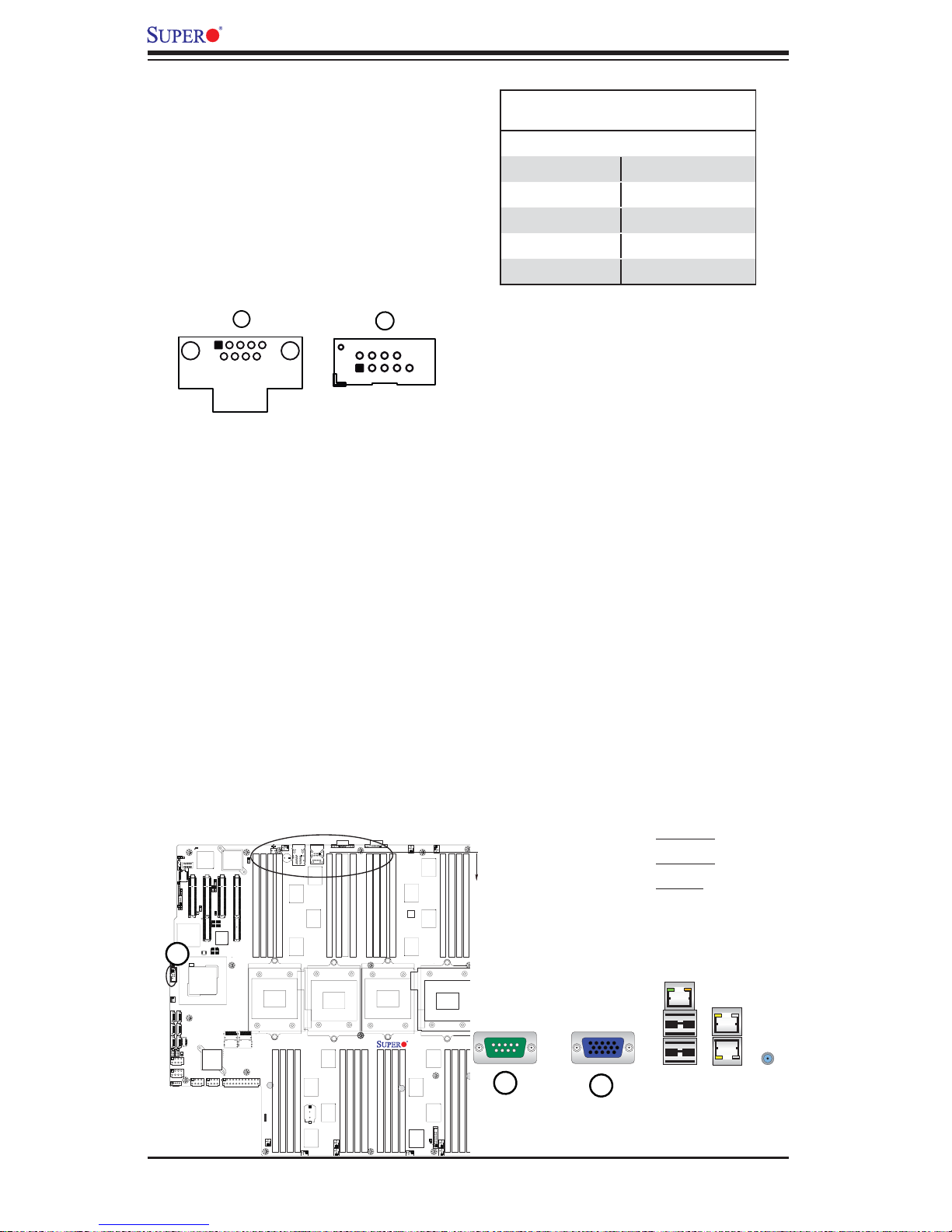
Serial Ports
Two COM connections (COM1 &
COM2) are located on the motherboard.
COM1 is located on the Backplane I/O
panel. COM2, located close to the 7500
IOH, provides front accessible serial
support. See the table on the right for
pin defi nitions.
Video Connection
Serial COM) Ports
Pin Defi nitions
Pin # Defi nition Pin # Defi nition
1 DCD 6 DSR
2 RXD 7 RTS
3 TXD 8 CTS
4 DTR 9 RI
5 Ground 10 N/A
A Video (VGA) port is located next to
COM1 on the I/O backplane. Refer
to the board layout below for the
location.
USB0/1
LAN1
LED26
JPRST1
JWOR
BMC_HB
D10
Intel 82576
IPMB
Winbond
BMCRST
J40
BMC CTRL
U101
JD1
JWD1
JLPC1
JP10
PORT80
1
Intel ICH 10R
USB5
I-SATA1
I-SATA3
J59
BBU
JP5
JL1
JPI2C1
Slot2 PCI-E 2.0 X16/X8
Slot1 PCI-E 2.0 X8
JPB1
JBT1
U70
BIOS
Intel
IOH 7500
LSI 2108
SAS CTRL
JPWR1JPWR2
JPS1
JPT1
JPG1
JUID_OW1
LAN CTRL
Slot3 PCI-E 2.0 X8
JP3
JP1
SAS0~3
JPWR3
JP4
J35
USB2/3
COM2
FAN 11
I-SATA0
I-SATA2
I-SATA5
I-SATA4
JP6
JPWR5
JPWR4
UID_LED
UID_SWITCH
JPL1
Slot4 PCI-E 2.0 X16/X8
P1-DIMM4A
SAS4~7
P5V_STBY
JUIDB1
P1-DIMM3A
LED5
LED7
LED8
LED9
LED6
FAN7
P1-DIMM2A
CPU1
P1-DIMM1A
P2-DIMM8A
FAN10
P2-DIMM7A
SP1
(LOWER)
(UPPER)
P2-DIMM6A
LAN2
P2-DIMM5A
IPMI_LAN
BT2
Battery
FAN6
P1-DIMM5A
CPU2
FAN4
FAN
VGA
P1-DIMM6A
P2-DIMM1A
P1-DIMM7A
P1-DIMM8A
P2-DIMM2A
P2-DIMM3A
P3-DIMM4A
P2-DIMM4A
COM1
P3-DIMM3A
P4-DIMM8A
P3-DIMM2A
CPU3
P4-DIMM7A
P3-DIMM1A
P4-DIMM6A
FAN9
X8QBE-F
Rev. 1.11
P4-DIMM5A
FAN3
OHLED
JOH1
FAN8
JF1
P3-DIMM6A
P3-DIMM7A
P3-DIMM5A
CPU4
P4-DIMM1A
P4-DIMM2A
FAN1
FAN2
3-12
P4-DIMM3A
P3-DIMM8A
-
1. COM1
2. COM2
3. VGA
Page 39
Chapter 3: Installation
5
P4
DIMM4A
1
2
3
4
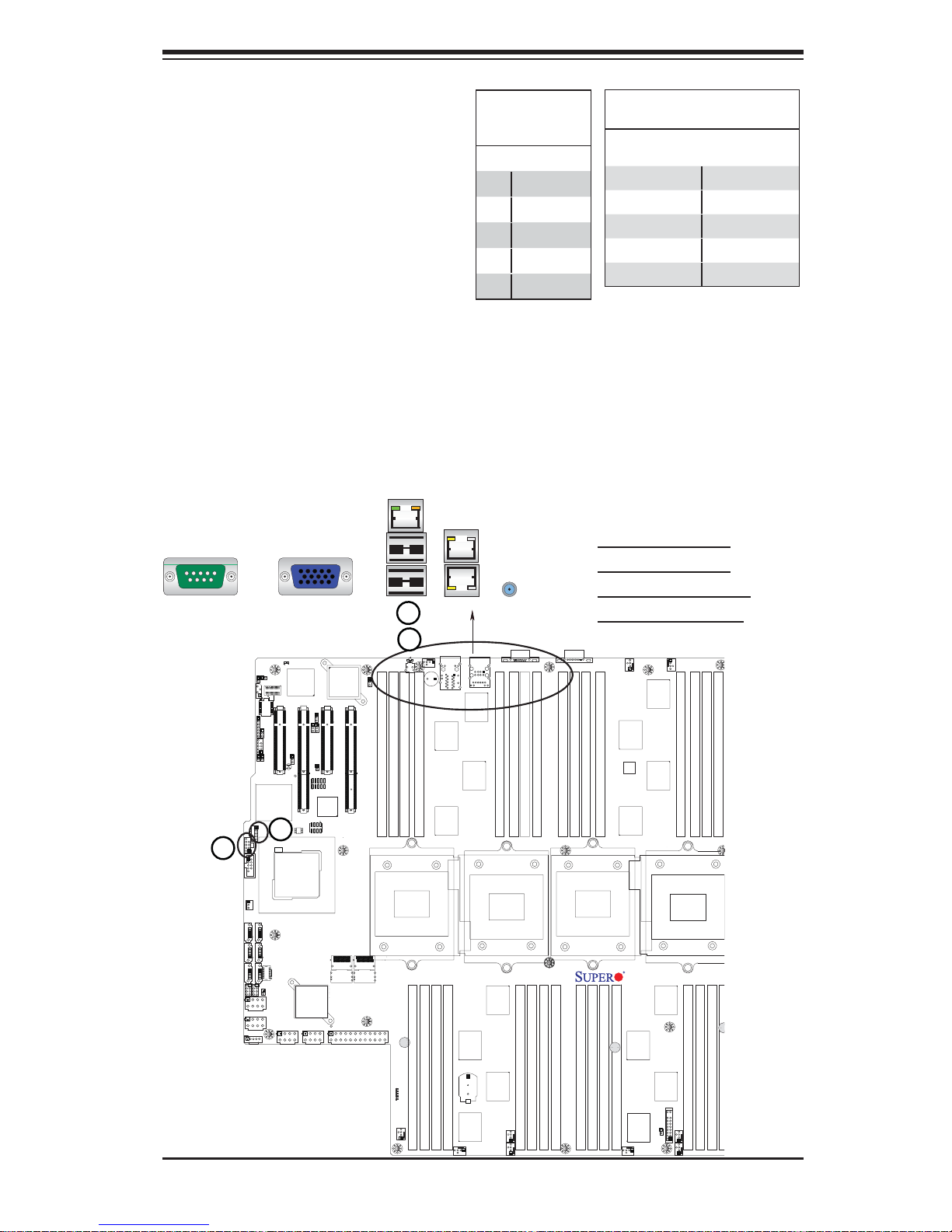
Universal Serial Bus (USB)
Two Universal Serial Bus ports (USB
0/1) are located on the I/O back panel.
Additional Front Panel USB connections (USB 2/3, USB5) are on the
motherboard to provide front chassis
access. (Cables are not included).
See the tables on the right for pin
defi nitions.
Backplane USB
(0/1)
Pin Defi nitions
Pin# Defi nition
1 +5V
2 PO3 PO+
4 Ground
5NA
FP USB (2/3, 5)
Pin Defi nitions
USB 2
Pin # Defi nition
USB 3/5
Pin # Defi nition
1 +5V 1 +5V
2 PO- 2 PO3 PO+ 3 PO+
4 Ground 4 Ground
5 NC 5 Key
(NC= No connection)
1. Backpanel USB 0
2. Backpanel USB 1
3. Front Panel USB 2/3
4. Front Panel USB 5
USB2/3
COM2
I-SATA0
I-SATA2
I-SATA4
JP6
J40
I-SATA5
JPWR5
JPWR4
JPRST1
JWOR
IPMB
BMCRST
JP4
U101
JD1
JWD1
JLPC1
JP10
PORT80
1
J35
Intel ICH 10R
USB5
FAN 11
I-SATA1
I-SATA3
J59
JP5
JL1
JPI2C1
D10
Slot1 PCI-E 2.0 X8
JPB1
JBT1
Intel
IOH 7500
BBU
Winbond
BMC CTRL
BMC_HB
JPS1
Slot2 PCI-E 2.0 X16/X8
JPT1
JPG1
JUID_OW1
JP3
U70
JP1
BIOS
LSI 2108
SAS CTRL
JPWR1JPWR2
Intel 82576
LAN CTRL
Slot4 PCI-E 2.0 X16/X8
Slot3 PCI-E 2.0 X8
SAS0~3
SAS4~7
JPWR3
UID_SWITCH
JPL1
P1-DIMM4A
P5V_STBY
UID_LED
JUIDB1
P1-DIMM3A
LED5
LED7
LED8
LED9
LED6
FAN7
LED26
P1-DIMM1A
P1-DIMM2A
CPU1
P2-DIMM8A
FAN10
SP1
P2-DIMM7A
LAN1
(LOWER)
LAN2
(UPPER)
P2-DIMM6A
P2-DIMM5A
FAN6
BT2
Battery
USB0/1
IPMI_LAN
P1-DIMM5A
P1-DIMM6A
CPU2
FAN4
FAN
VGA
P1-DIMM7A
P2-DIMM1A
P1-DIMM8A
P2-DIMM2A
P2-DIMM3A
COM1
P3-DIMM4A
P2-DIMM4A
P3-DIMM2A
P3-DIMM3A
P4-DIMM8A
CPU3
P4-DIMM7A
P3-DIMM1A
P4-DIMM6A
FAN9
X8QBE-F
Rev. 1.11
P4-DIMM5A
FAN3
FAN8
JF1
OHLED
JOH1
P3-DIMM5A
CPU4
FAN1
FAN2
P3-DIMM6A
P4-DIMM1A
P4-DIMM2A
P3-DIMM8A
P3-DIMM7A
P4-DIMM3A
-
3-13
Page 40
X8QB6-F/X8QBE-F Motherboard User's Manual
1
2
3
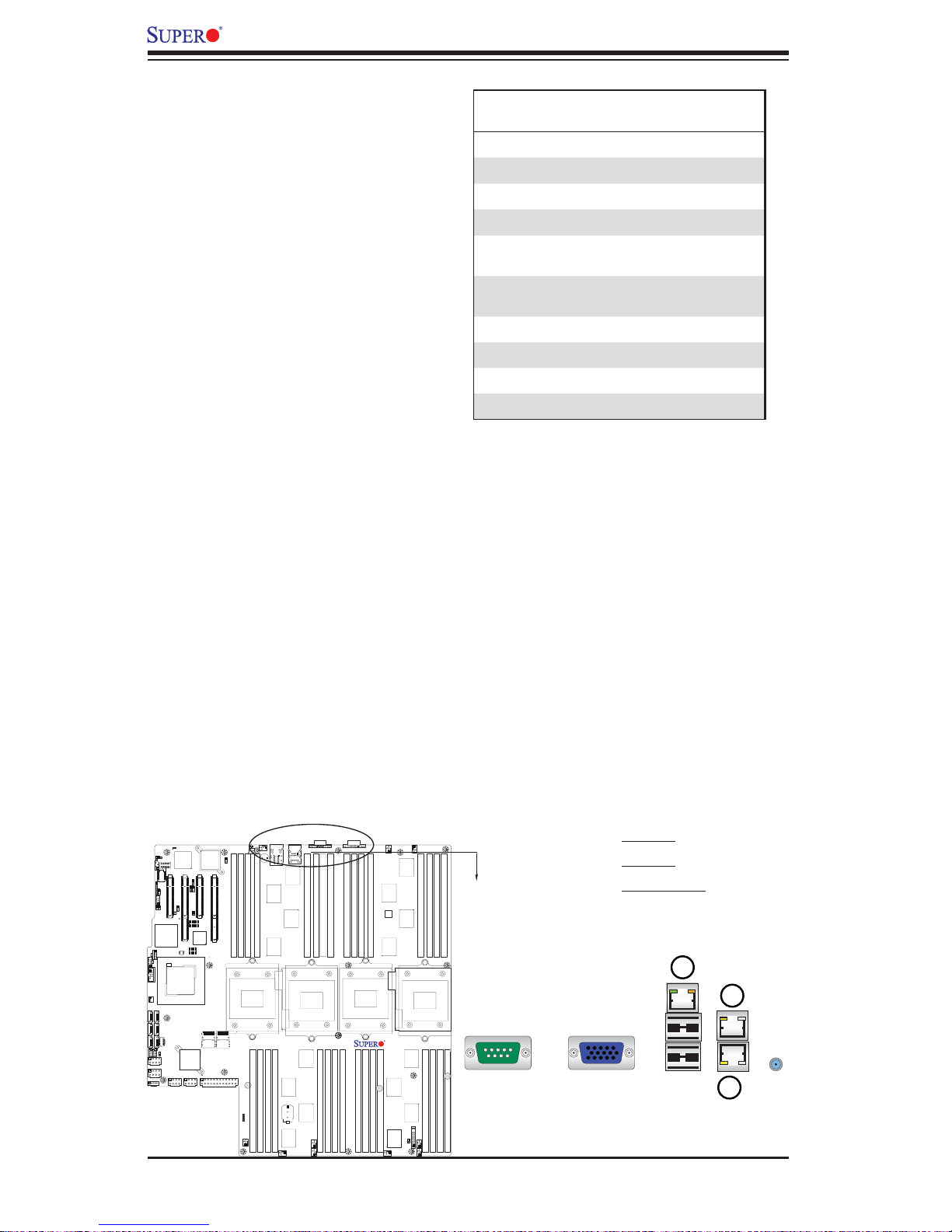
Ethernet Ports
Two Ethernet ports (LAN1/LAN2) are
located on the I/O backplane on the
motherboard. In addition, an IPMI_
Dedicated LAN is located above USB
0/1 ports on the backplane to provide
KVM support for IPMI 2.0. All these
ports accept RJ45 type cables. (Note:
Please refer to the LED Indicator Section for LAN LED information.)
LAN Ports
Pin Defi nition
Pin# Defi nition
1 P2V5SB 10 SGND
2 TD0+ 11 Act LED
3 TD0- 12 P3V3SB
4 TD1+ 13 Link 100 LED (Yel-
low, +3V3SB)
5 TD1- 14 Link 1000 LED
(Yellow, +3V3SB)
6 TD2+ 15 Ground
7 TD2- 16 Ground
8 TD3+ 17 Ground
9 TD3- 18 Ground
(NC: No Connection)
X8QBE-F
Rev. 1.11
1. LAN1
2. LAN2
3. IPMI_LAN
3-14
Page 41
Chapter 3: Installation
2
1
3
1
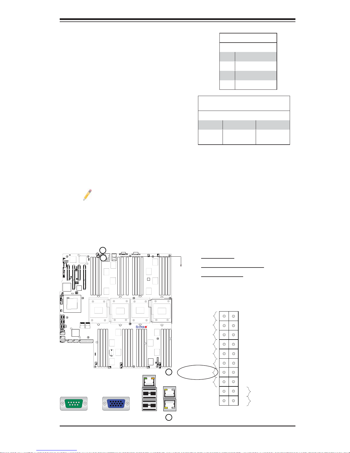
Unit Identifi er Switch
A Unit Identifi er (UID) Switch and two LED
Indicators are located on the motherboard.
The UID Switch is located next to the LAN
ports on the backplane. The Rear UID LED
(LED26) is located next to the UID Switch.
The Front Panel UID LED is located at Pins
7/8 of the Front Control Panel at JF1. Connect a cable to Pin 8 on JF1 for Front Panel
UID LED indication. When you press the
UID switch, both Rear UID LED and Front
Panel UID LED Indicators will be turned on.
Press the UID switch again to turn off both
LED Indicators. These UID Indicators provide
easy identifi cation of a system unit that may
be in need of service.
Note: UID can also be triggered via
IPMI on the motherboard. For more
information on IPMI, please refer to
the IPMI User's Guide posted on
our Website @http://www.supermicro.com.
UID Switch
Pin# Defi nition
1 Ground
2 Ground
3 Button In
4 Ground
UID LED (LE2)
Status
Color/State OS Status
Blue: On Windows OS Unit Identifi ed
Blue:
Blinking
Linux OS Unit Identifi ed
X8QBE-F
Rev. 1.11
1. UID Switch
2. Rear UID LED (LED26)
3. Front UID LED
Ground
X
FP PWRLED
HDD LED
NIC1 Link LED
NIC2 Link LED
Blue+ (OH/Fan Fail/
PWR FaiL/UID LED)
Power Fail LED
Ground
Ground
1920
NMI
X
3.3 V
ID_UID_SW/3/3V Stby
NIC1 Activity LED
NIC2 Activity LED
Red+ (Blue LED Cathode)
3.3V
Reset
Reset Button
Powe r Button
PWR
2
1
3-15
Page 42
X8QB6-F/X8QBE-F Motherboard User's Manual
5
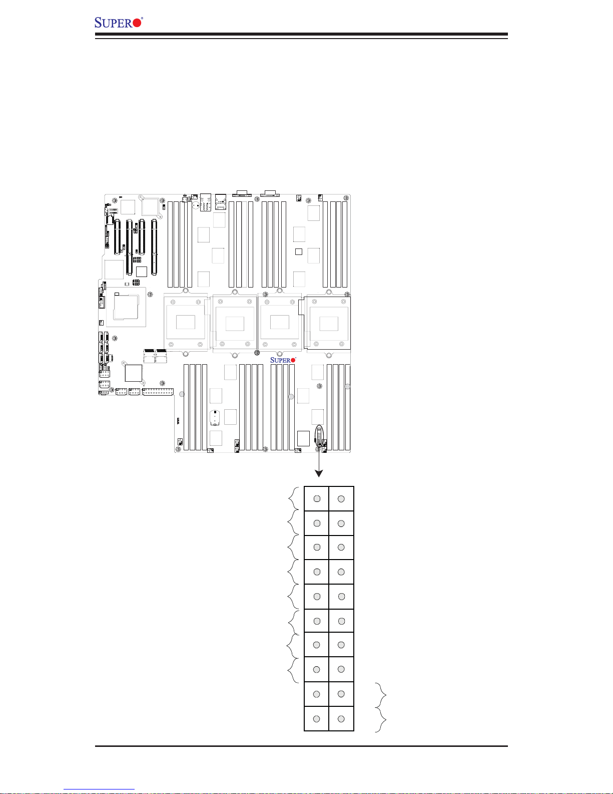
Front Control Panel
JF1 contains header pins for various buttons and indicators that are normally located on a control panel at the front of the chassis. These connectors are designed
specifi cally for use with Supermicro's server chassis. See the fi gure below for the
descriptions of the various control panel buttons and LED indicators. Refer to the
following section for descriptions and pin defi nitions.
JF1 Header Pins
USB0/1
JP6
USB2/3
COM2
I-SATA0
I-SATA2
I-SATA4
JPWR5
JPWR4
JWOR
J40
JP4
JD1
1
J35
USB5
FAN 11
I-SATA5
JP5
JPRST1
D10
IPMB
BMCRST
U101
JWD1
JLPC1
JP10
PORT80
Intel ICH 10R
I-SATA1
I-SATA3
J59
BBU
JL1
JPI2C1
BMC_HB
Winbond
BMC CTRL
Slot2 PCI-E 2.0 X16/X8
Slot1 PCI-E 2.0 X8
JPT1
JUID_OW1
JPB1
JBT1
U70
BIOS
Intel
IOH 7500
LSI 2108
SAS CTRL
JPWR1JPWR2
JPS1
JPG1
Intel 82576
LAN CTRL
Slot3 PCI-E 2.0 X8
JP3
JP1
SAS0~3
JPWR3
UID_LED
JUIDB1
UID_SWITCH
JPL1
Slot4 PCI-E 2.0 X16/X8
P1-DIMM4A
SAS4~7
P5V_STBY
LED26
P1-DIMM3A
P1-DIMM2A
LED5
LED7
LED8
LED9
LED6
FAN7
CPU1
P2-DIMM8A
FAN10
SP1
P1-DIMM1A
P2-DIMM7A
LAN1
(LOWER)
LAN2
(UPPER)
P2-DIMM6A
P2-DIMM5A
Battery
FAN6
BT2
IPMI_LAN
P1-DIMM5A
CPU2
FAN4
FAN
VGA
P1-DIMM6A
P1-DIMM7A
P2-DIMM1A
P1-DIMM8A
P2-DIMM2A
P2-DIMM4A
P2-DIMM3A
COM1
P3-DIMM4A
P3-DIMM3A
P3-DIMM2A
CPU3
P4-DIMM8A
P4-DIMM7A
P3-DIMM1A
P4-DIMM6A
FAN9
X8QBE-F
Rev. 1.11
P4-DIMM5A
FAN3
FAN8
OHLED
JOH1
P3-DIMM6A
P3-DIMM8A
P3-DIMM7A
P3-DIMM5A
CPU4
P4-DIMM4A
P4-DIMM3A
P4-DIMM1A
P4-DIMM2A
JF1
FAN1
FAN2
Ground
X
FP PWRLED
HDD LED
NIC1 Link LED
NIC2 Link LED
Blue+ (OH/Fan Fail/
PWR FaiL/UID LED)
Power Fail LED
Ground
Ground
3-16
1920
NMI
X
3.3 V
ID_UID_SW/3/3V Stby
NIC1 Activity LED
NIC2 Activity LED
Red+ (Blue LED Cathode)
3.3V
Reset
PWR
2
1
Reset Button
Power Button
Page 43
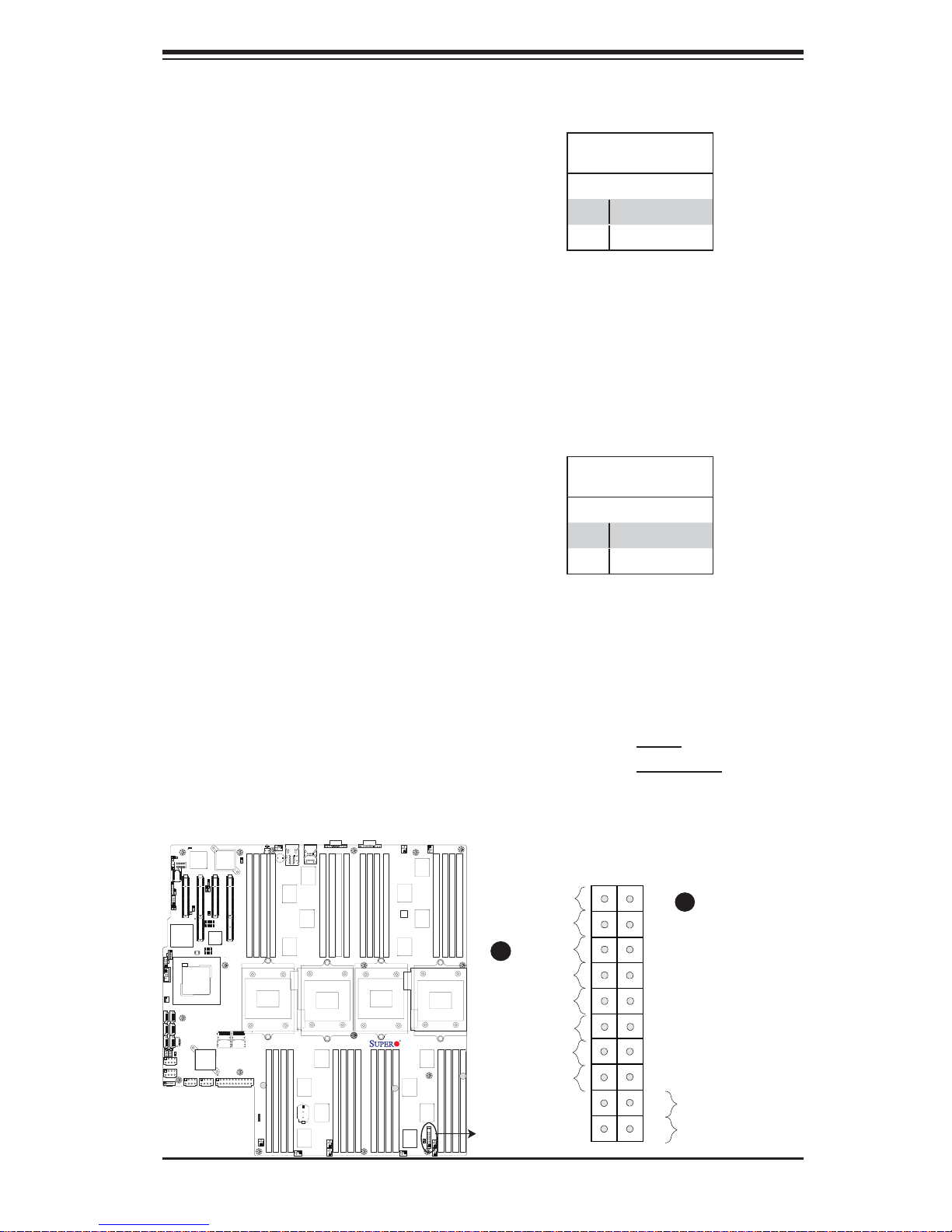
Front Control Panel Pin Defi nitions
Chapter 3: Installation
NMI Button
The non-maskable interrupt button
header is located on pins 19 and 20
of JF1. Refer to the table on the right
for pin defi nitions.
Power LED
The Power LED connection is located
on pins 15 and 16 of JF1. Refer to the
table o n the ri ght for p in defi nitions.
NMI Button
Pin Defi nitions (JF1)
Pin# Defi nition
19 Control
20 Ground
Power LED
Pin Defi nitions (JF1)
Pin# Defi nition
15 3.3V
16 PWR LED
X8QBE-F
Rev. 1.11
FP PWRLED
B
HDD LED
NIC1 Link LED
NIC2 Link LED
Blue+ (OH/Fan Fail/
PWR FaiL/UID LED)
Power Fail LED
3-17
Ground
X
Ground
Ground
A. NMI
B. PWR LED
1920
2
1
NMI
A
X
3.3 V
ID_UID_SW/3/3V Stby
NIC1 Activity LED
NIC2 Activity LED
Red+ (Blue LED Cathode)
3.3V
Reset
Reset Button
Powe r Button
PWR
Page 44
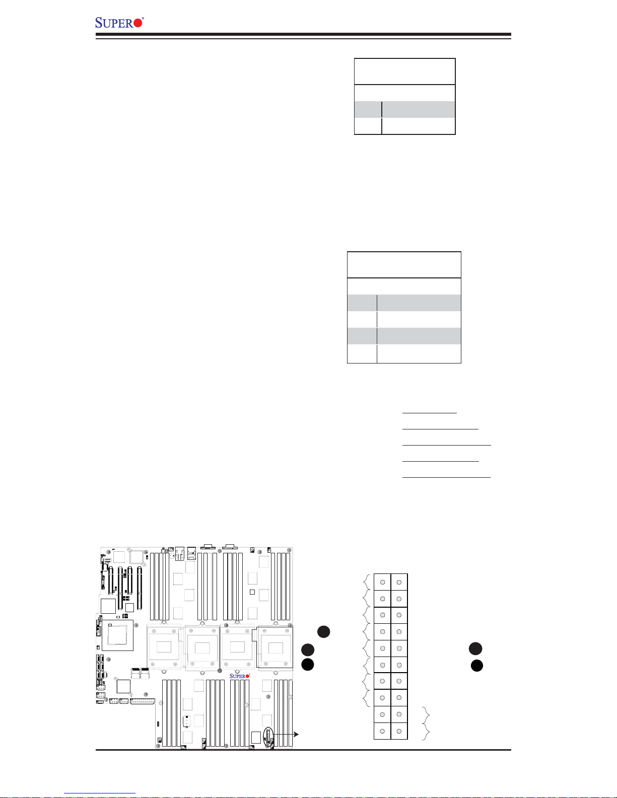
X8QB6-F/X8QBE-F Motherboard User's Manual
D
E
HDD LED
The HDD LED connection is located
on pins 13 and 14 of JF1. Attach a
cable here to indicate HDD activity. See the table on the right for pin
defi nitions.
NIC1/NIC2 LED Indicators
The NIC (Network Interface Controller) LED connection for GLAN port 1 is
located on pins 11 and 12 of JF1, and
the LED connection for GLAN Port 2 is
on Pins 9 and 10. Attach the NIC LED
cables here to display network activity .
Refer to the table on the right for pin
defi nitions.
HDD LED
Pin Defi nitions (JF1)
Pin# Defi nition
13 3.3V Standby
14 HD Active
GLAN1/2 LED
Pin Defi nitions (JF1)
Pin# Defi nition
9 NIC 2 Activity LED
10 NIC 2 Link LED
11 NIC 1 Activity LED
12 NIC 1 Link LED
X8QBE-F
Rev. 1.11
Ground
X
FP PWRLED
HDD LED
A
NIC1 Link LED
B
NIC2 Link LED
Blue+ (OH/Fan Fail/
PWR FaiL/UID LED)
Power Fail LED
Ground
Ground
A. HDD LED
B. NIC1 Link LED
C. NIC1 Activity LED
D. NIC2 Link LED
E. NIC2 Activity LED
1920
NMI
X
3.3 V
ID_UID_SW/3/3V Stby
NIC1 Activity LED
NIC2 Activity LED
Red+ (Blue LED Cathode)
3.3V
Reset
Reset Button
Power Button
PWR
2
1
C
3-18
Page 45
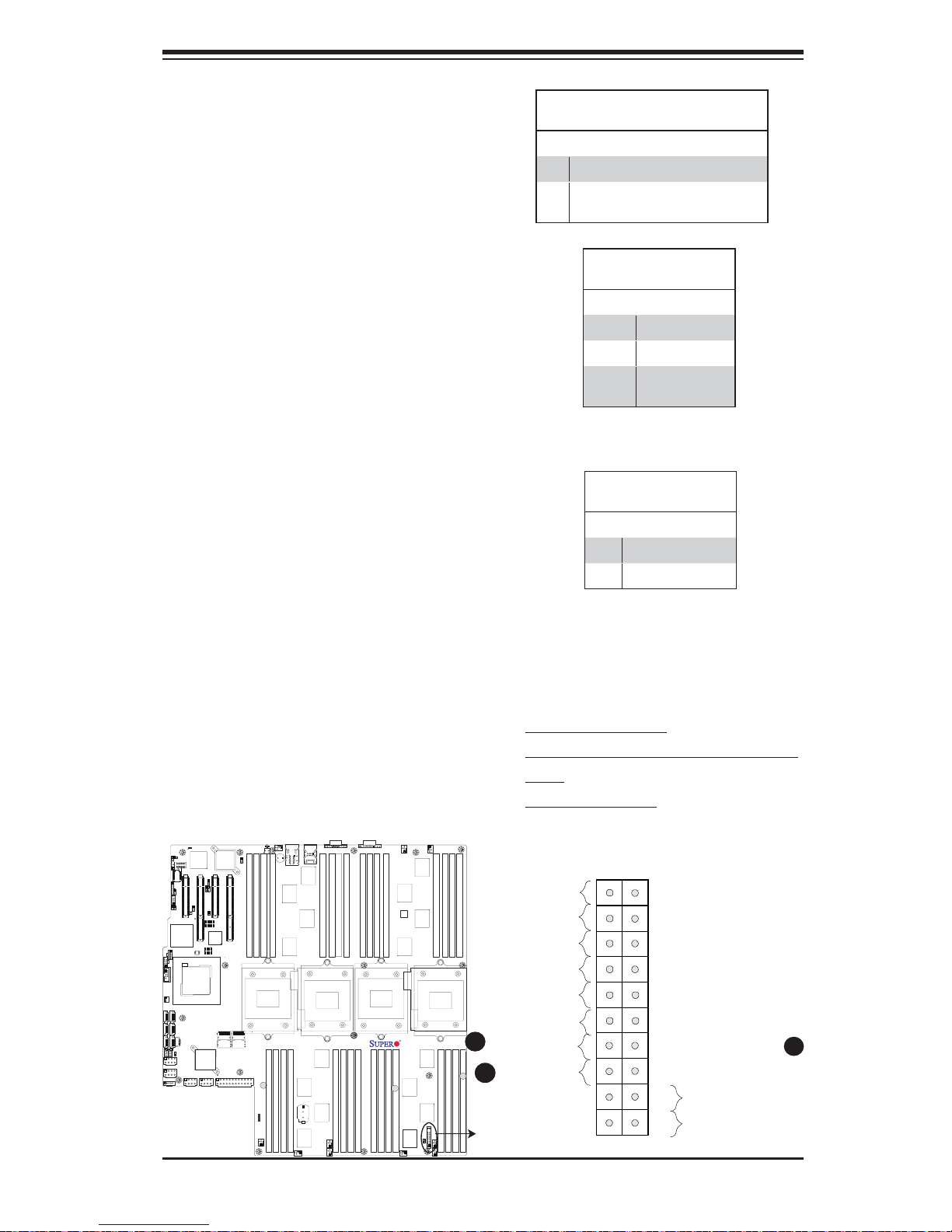
Chapter 3: Installation
Overheat (OH)/Fan Fail/PWR Fail/
UID LED
Connect an LED cable to OH/Fan Fail/
Front UID LED connection on pins 7
and 8 of JF1 to provide advanced
warnings of chassis overheat or fan
failure. It also works as the front panel
UID LED indicator. The Red LED
takes pr ec ed enc e over t he B lue L ED
by default. Refer to the table on the
right for pin defi nitions.
Power Fail LED
The Power Fail LED connection is
locate d on pins 5 and 6 of JF1. Refer to the table on the right for pin
defi nitions.
OH/Fan Fail/PWR Fail/UID LED
Pin Defi nitions (JF1)
Pin# Defi nition
7 Red+ (Blue LED Cathode)
8 Blue+ (OH/Fan Fail/PWR Fail/
UID LED)
OH/Fan Fail Indicator
Status
State Defi nition
Off Normal
On Overheat
Flash-
ing
Pin# Defi nition
5 3.3V
6 PWR Supply Fail
Fan Fail
PWR Fail LED
Pin Defi nitions (JF1)
X8QBE-F
Rev. 1.11
A. Blue LED Cathode
B. OH/Fail/PWR Fail LED (Red)/UID
(Blue)
C. PWR Supply Fail
FP PWRLED
HDD LED
NIC1 Link LED
NIC2 Link LED
Blue+ (OH/Fan Fail/
B
PWR FaiL/UID LED)
Power Fail LED
C
Ground
X
Ground
Ground
1920
NMI
X
3.3 V
ID_UID_SW/3/3V Stby
NIC1 Activity LED
NIC2 Activity LED
Red+ (Blue LED Cathode)
3.3V
Reset
Reset Button
Powe r Button
PWR
2
1
A
3-19
Page 46
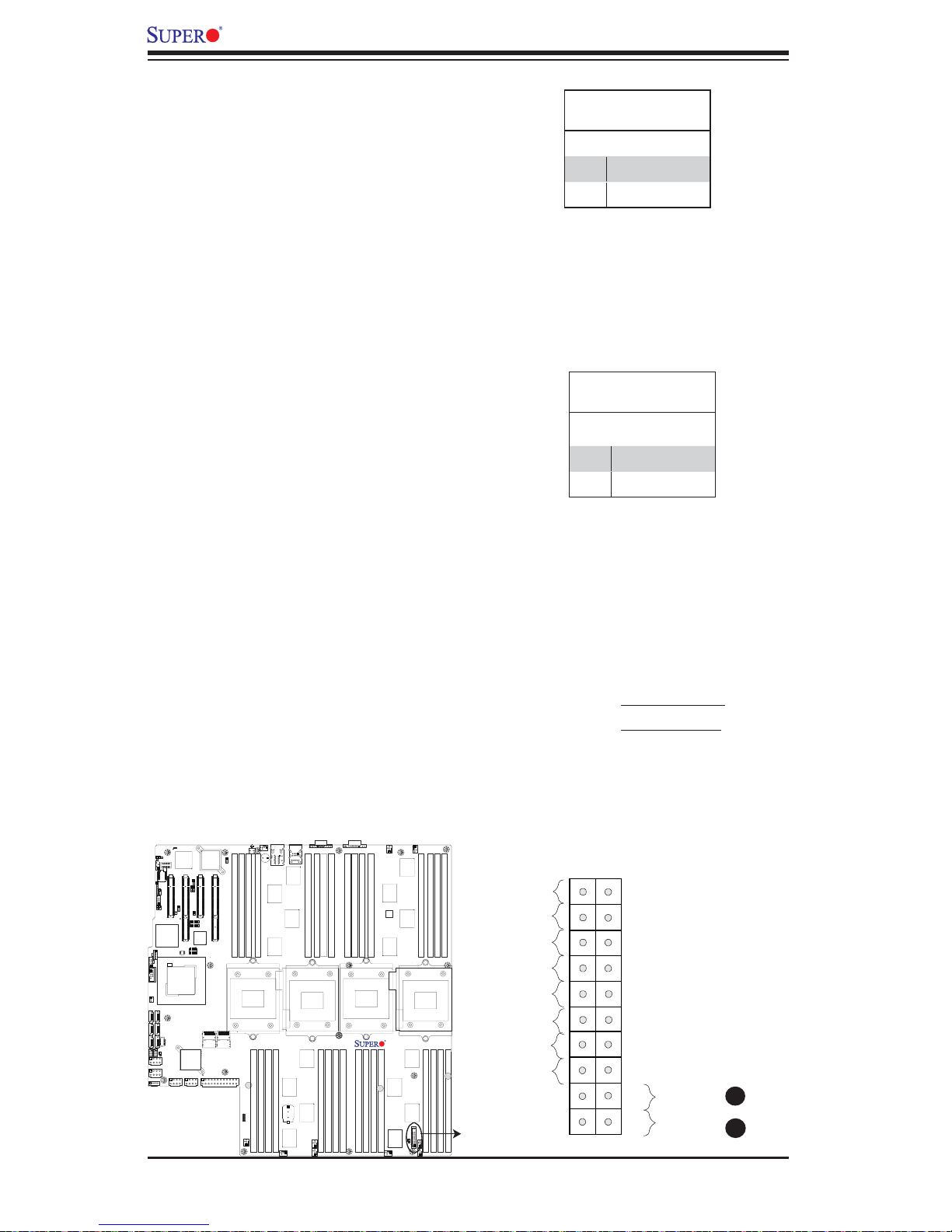
X8QB6-F/X8QBE-F Motherboard User's Manual
Reset Button
The Reset Button connection is located
on pins 3 and 4 of JF1. Attach it to a
hardware reset switch on the computer
case. Refer to the table on the right for
pin defi nitions.
Power Button
The Power Button connection is located
on pins 1 and 2 of JF1. Momentarily
contacting both pins will power on/off
the system. This button can also be confi gured to function as a suspend button
(with a setting in the BIOS - See Chapter
5). To turn off the power when the system
is in suspend mode, press the button for
4 seconds or longer. Refer to the table on
the right for pin defi nitions.
Reset Button
Pin Defi nitions (JF1)
Pin# Defi nition
3 Reset
4 Ground
Power Button
Pin Defi nitions (JF1)
Pin# Defi nition
1 Signal
2 Ground
X8QBE-F
Rev. 1.11
Ground
FP PWRLED
HDD LED
NIC1 Link LED
NIC2 Link LED
Blue+ (OH/Fan Fail/
PWR FaiL/UID LED)
Power Fail LED
Ground
Ground
A. Reset Button
B. PWR Button
1920
NMI
X
2
X
3.3 V
ID_UID_SW/3/3V Stby
NIC1 Activity LED
NIC2 Activity LED
Red+ (Blue LED Cathode)
3.3V
Reset
Reset Button
Power Button
PWR
1
A
B
3-20
Page 47
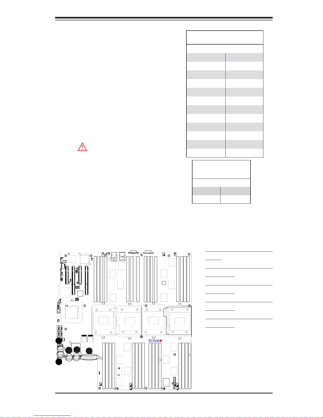
Chapter 3: Installation
5
D
E
3-6 Connecting Cables
Power Connectors
A 24-pin main power supply
connector(JPWR3) and four 8-pin CPU
PWR connectors (JPWR1~2, JPWR4~5)
are located on the motherboard. These power connectors meet the SSI EPS 12V specifi cation. These power connectors must also
be connected to your power supply . See the
table on the right for pin defi nitions.
Warning: To provide adequate
power supply to the motherboard,
be sure to connect the 24-pin
ATX PWR (JPWR3) and three
8-pin PWR connectors (JPWR1,
JPWR2, JPWR4, or JPWR5) to
the power supply. Failure to do
so will void the manufacturer warranty on your power supply and
motherboard. Also, be sure to use
a power supply that supports the
specifi cations listed in the table on
USB2/3
COM2
I-SATA0
I-SATA2
I-SATA4
JP6
JPWR5
JPWR4
JWOR
J40
JP4
JD1
1
J35
USB5
FAN 11
I-SATA5
JP5
JPRST1
D10
IPMB
BMCRST
U101
JWD1
JLPC1
JP10
PORT80
Intel ICH 10R
I-SATA1
I-SATA3
J59
BBU
JL1
C
JPI2C1
BMC_HB
Winbond
BMC CTRL
Slot2 PCI-E 2.0 X16/X8
Slot1 PCI-E 2.0 X8
JPT1
JUID_OW1
JPB1
JBT1
U70
BIOS
Intel
IOH 7500
LSI 2108
SAS CTRL
B
JPWR1JPWR2
Page 2-3 or Page 2-6.
LED26
UID_LED
JUIDB1
UID_SWITCH
JPL1
Intel 82576
LAN CTRL
JPS1
Slot4 PCI-E 2.0 X16/X8
Slot3 PCI-E 2.0 X8
JPG1
JP3
JP1
SAS0~3
JPWR3
A
SAS4~7
P1-DIMM3A
P1-DIMM4A
LED5
P5V_STBY
LED6
LED7
LED8
LED9
FAN7
P1-DIMM2A
CPU1
P2-DIMM8A
FAN10
SP1
P1-DIMM1A
P2-DIMM7A
LAN1
(LOWER)
LAN2
(UPPER)
P2-DIMM6A
P2-DIMM5A
Battery
FAN6
BT2
USB0/1
IPMI_LAN
P1-DIMM5A
CPU2
FAN4
FAN
VGA
P1-DIMM6A
P1-DIMM7A
P2-DIMM1A
P1-DIMM8A
P2-DIMM2A
P2-DIMM3A
COM1
P3-DIMM4A
P2-DIMM4A
P3-DIMM2A
P3-DIMM3A
P4-DIMM8A
P3-DIMM1A
CPU3
P4-DIMM7A
P4-DIMM6A
P4-DIMM5A
FAN9
X8QBE-F
Rev. 1.11
FAN3
FAN8
OHLED
JOH1
ATX Power 24-pin Connector
Pin Defi nitions
Pin# Defi nition Pin # Defi nition
13 +3.3V 1 +3.3V
14 -12V 2 +3.3V
15 COM 3 COM
16 PS_ON 4 +5V
17 COM 5 COM
18 COM 6 +5V
19 COM 7 COM
20 Res (NC) 8 PWR_OK
21 +5V 9 5VSB
22 +5V 10 +12V
23 +5V 11 +12V
24 COM 12 +3.3V
12V 8-pin PWR Con-
nector
Pin Defi nitions
Pins Defi nition
1 through 4 Ground
5 through 8 +12V
(Required)
A. JPWR3: 24-pin ATX PWR
(Req'd)
B. JPWR1: 8-pin Processor
P3-DIMM6A
P3-DIMM8A
P3-DIMM7A
P3-DIMM5A
PWR (Req'd)
C. JPWR2: 8-pin Processor
PWR (Req'd)
D. JPWR4: 8-pin Processor
PWR (Req'd)
CPU4
E. JPWR5: 8-pin Processor
PWR (Req'd)
P4-DIMM4A
P4-DIMM3A
P4-DIMM1A
P4-DIMM2A
JF1
FAN1
FAN2
3-21
Page 48
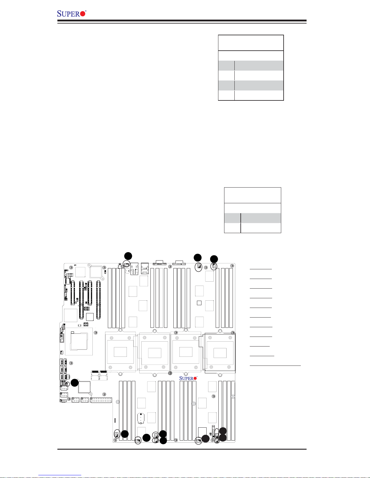
X8QB6-F/X8QBE-F Motherboard User's Manual
5
D
E
F
G
Fan Headers
This motherboard has ten system/CPU
fan headers (Fan 1 to Fan10) on the
motherboard. (Fan 11: reserved) All
these 4-pin fans headers are backward
compatible with the traditional 3-pin fans.
However, fan speed control is available
for 4-pin fans only. The fan speeds are
controlled by Thermal Management via
Hardware Monitoring in the Advanced
Setting in the BIOS. (See Chapter 5 for
more details.) See the table on the right
for pin defi nitions.
Chassis Intrusion
A Chassis Intrusion header is located
at JL1 on the motherboard. Attach an
appropriate cable from the chassis to
inform you of a chassis intrusion when
the chassis is opened.
Fan Header
Pin Defi nitions
Pin# Defi nition
1 Ground
2 +12V
3 Tachometer
4 PWR Modulation
Chassis Intrusion
Pin Defi nitions
Pin# Defi nition
1 Intrusion Input
2 Ground
USB2/3
COM2
I-SATA0
I-SATA2
I-SATA4
JP6
J40
FAN 11
I-SATA5
JPWR5
JPWR4
JPRST1
JWOR
IPMB
BMCRST
JP4
U101
JD1
JWD1
JLPC1
JP10
PORT80
1
J35
Intel ICH 10R
USB5
I-SATA1
I-SATA3
J59
JP5
JL1
JPI2C1
D10
BMC CTRL
Slot1 PCI-E 2.0 X8
JPB1
JBT1
Intel
IOH 7500
BBU
K
BMC_HB
Winbond
Intel 82576
LAN CTRL
JPS1
Slot2 PCI-E 2.0 X16/X8
JPT1
JPG1
JUID_OW1
JP3
U70
JP1
BIOS
LSI 2108
SAS CTRL
JPWR1JPWR2
Slot4 PCI-E 2.0 X16/X8
Slot3 PCI-E 2.0 X8
SAS0~3
SAS4~7
JPWR3
UID_SWITCH
JPL1
P1-DIMM4A
P5V_STBY
UID_LED
JUIDB1
LED26
P1-DIMM3A
P1-DIMM2A
LED5
LED7
LED8
LED9
LED6
FAN7
CPU1
P2-DIMM8A
J
FAN10
SP1
P1-DIMM1A
P2-DIMM7A
LAN1
(LOWER)
LAN2
(UPPER)
P2-DIMM6A
P2-DIMM5A
FAN6
Battery
BT2
USB0/1
IPMI_LAN
P1-DIMM5A
CPU2
FAN4
FAN
VGA
P1-DIMM6A
P1-DIMM7A
P2-DIMM1A
P1-DIMM8A
P2-DIMM2A
P2-DIMM3A
COM1
P3-DIMM4A
P2-DIMM4A
P3-DIMM2A
P3-DIMM3A
P4-DIMM8A
CPU3
P4-DIMM7A
P3-DIMM1A
P4-DIMM6A
I
FAN9
X8QBE-F
Rev. 1.11
P4-DIMM5A
FAN3
H
FAN8
A. Fan 1
B. Fan 2
C. Fan 3
P3-DIMM6A
P3-DIMM8A
P3-DIMM7A
P3-DIMM5A
D. Fan 4
E. Fan 5
F. Fan 6
G. Fan 7
H. Fan 8
I. Fan 9
CPU4
J. Fan 10
K. Chassis Intrusion
P4-DIMM4A
P4-DIMM3A
P4-DIMM1A
P4-DIMM2A
JF1
OHLED
FAN1
A
JOH1
B
C
FAN2
3-22
Page 49
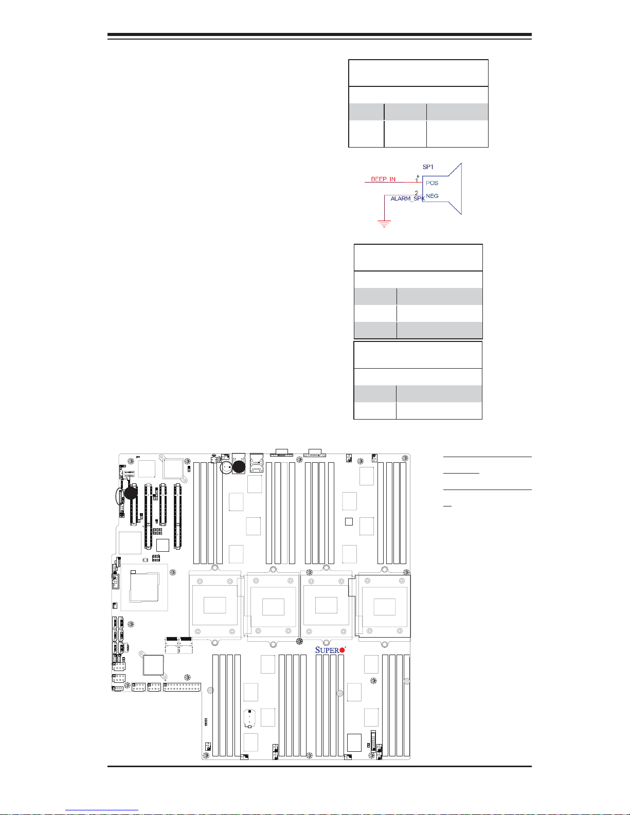
Chapter 3: Installation
5
Internal Speaker
The Internal Speaker, located at SP1,
can be used to provide audible indications for various beep codes. See the
table on the right for pin defi nitions.
Refer to the layout below for the locations of the Internal Buzzer (SP1).
Power LED/Speaker
On the JD1 header, pins 1-3 are
used for power LED indication, and
pins 4-7 are for the speaker. See the
tables on the right for pin defi nitions.
Please note that the speaker connector pins (4-7) are used with an
external speaker. If you wish to use
the onboard speaker, you should close
pins 6-7 with a jumper.
Internal Buzzer (SP1)
Pin Defi nition
Pin# Defi nitions
Pin 1 Pos. (+) Beep In
Pin 2 Neg. (-) Alarm
Speaker
PWR LED Connector
Pin Defi nitions
Pin Setting Defi nition
Pin 1 Anode (+)
Pin2 Cathode (-)
Pin3 NA
Speaker Connector
Pin Settings
Pin Setting Defi nition
Pins 4-7 External Speaker
Pins 6-7 Internal Speaker
USB2/3
COM2
I-SATA0
I-SATA2
I-SATA4
JP6
I-SATA5
JPWR5
JPWR4
JPRST1
JWOR
IPMB
BMCRST
J40
JP4
U101
JD1
JWD1
B
JLPC1
JP10
PORT80
1
J35
Intel ICH 10R
USB5
FAN 11
I-SATA1
I-SATA3
J59
JP5
JL1
JPI2C1
D10
JBT1
BBU
BMC CTRL
Slot1 PCI-E 2.0 X8
JPB1
Intel
IOH 7500
BMC_HB
Winbond
JPS1
Slot2 PCI-E 2.0 X16/X8
JPT1
JPG1
JUID_OW1
U70
JP1
BIOS
LSI 2108
SAS CTRL
JPWR1JPWR2
Intel 82576
LAN CTRL
Slot3 PCI-E 2.0 X8
JP3
SAS0~3
JPWR3
UID_LED
JUIDB1
UID_SWITCH
JPL1
Slot4 PCI-E 2.0 X16/X8
P1-DIMM3A
P1-DIMM4A
SAS4~7
LED5
P5V_STBY
LED6
LED7
LED8
LED9
FAN7
LED26
P1-DIMM1A
P1-DIMM2A
CPU1
P2-DIMM8A
FAN10
SP1
P2-DIMM6A
P2-DIMM7A
LAN1
(LOWER)
A
LAN2
(UPPER)
P2-DIMM5A
FAN6
BT2
Battery
USB0/1
IPMI_LAN
P1-DIMM5A
P1-DIMM6A
CPU2
FAN4
FAN
VGA
P1-DIMM7A
P2-DIMM1A
P1-DIMM8A
P2-DIMM2A
P2-DIMM3A
COM1
P3-DIMM4A
P2-DIMM4A
P3-DIMM2A
P3-DIMM3A
P4-DIMM8A
P3-DIMM1A
CPU3
P4-DIMM7A
P4-DIMM6A
P4-DIMM5A
FAN9
X8QBE-F
Rev. 1.11
FAN3
FAN8
JF1
OHLED
JOH1
P3-DIMM5A
CPU4
P4-DIMM1A
FAN1
FAN2
P3-DIMM6A
P3-DIMM7A
P4-DIMM2A
P3-DIMM8A
P4-DIMM4A
P4-DIMM3A
A. Internal Speaker
(Buzzer)
B. PWR LED/Speaker
3-23
Page 50
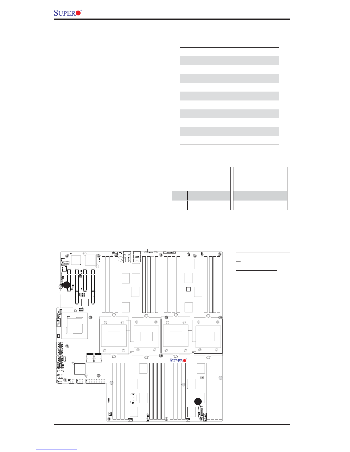
X8QB6-F/X8QBE-F Motherboard User's Manual
5
TPM Header/Port 80
A Trusted Platform Module/Port 80
header is located at LPCI to provide
TPM support and Port 80 connection.
Use this header to enhance system
performance and data security. See
the table on the right for pin defi ni-
tions.
Overheat LED/Fan Fail
The JOH1 header is used to connect
an LED indi cat or to p rovi de war ni ngs
of chassis overheating and fan failure.
This LED w ill b link w he n a fan f ailu re
occurs. Refer to the tables on right for
pin defi nitions.
TPM/Port 80 Header
Pin Defi nitions
Pin # Defi nition Pin # Defi nition
1 LCLK 2 GND
3 LFRAME# 4 <(KEY)>
5 LRESET# 6 +5V (X)
7 LAD 3 8 LAD 2
9 +3.3V 10 LAD1
11 LAD0 12 GND
13 SMB_CLK4 14 SMB_DAT4
15 +3V_DUAL 16 SERIRQ
17 GND 18 CLKRUN# (X)
19 LPCPD# 20 LDRQ# (X)
Overheat LED
Pin Defi nitions
Pin# Defi nition
1 5vDC
2 OH Active
OH/Fan Fail LED
Status
State Message
Solid Overheat
Blinking Fan Fail
USB2/3
COM2
I-SATA0
I-SATA2
I-SATA4
JP6
J40
FAN 11
I-SATA5
JPWR5
JPWR4
JPRST1
JWOR
IPMB
BMCRST
JP4
U101
JD1
JWD1
JLPC1
JP10
PORT80
1
A
J35
Intel ICH 10R
USB5
I-SATA1
I-SATA3
J59
JP5
JL1
JPI2C1
D10
BMC CTRL
Slot1 PCI-E 2.0 X8
JPB1
JBT1
Intel
IOH 7500
BBU
BMC_HB
Winbond
Intel 82576
LAN CTRL
JPS1
Slot2 PCI-E 2.0 X16/X8
JPT1
JPG1
JUID_OW1
JP3
U70
JP1
BIOS
LSI 2108
SAS CTRL
JPWR1JPWR2
Slot4 PCI-E 2.0 X16/X8
Slot3 PCI-E 2.0 X8
SAS0~3
SAS4~7
JPWR3
UID_SWITCH
JPL1
P1-DIMM4A
P5V_STBY
UID_LED
JUIDB1
LED26
P1-DIMM3A
P1-DIMM2A
LED5
LED7
LED8
LED9
LED6
FAN7
CPU1
P2-DIMM8A
FAN10
SP1
P1-DIMM1A
P2-DIMM7A
LAN1
(LOWER)
LAN2
(UPPER)
P2-DIMM6A
P2-DIMM5A
FAN6
Battery
BT2
USB0/1
IPMI_LAN
P1-DIMM5A
CPU2
FAN4
FAN
VGA
P1-DIMM6A
P1-DIMM7A
P2-DIMM1A
P1-DIMM8A
P2-DIMM2A
P2-DIMM3A
COM1
P3-DIMM4A
P2-DIMM4A
P3-DIMM2A
P3-DIMM3A
P4-DIMM8A
CPU3
P4-DIMM7A
P3-DIMM1A
P4-DIMM6A
FAN9
X8QBE-F
Rev. 1.11
P4-DIMM5A
FAN3
A. TPM/Port 80 Head-
FAN8
er
B. Overheat LED
P3-DIMM6A
P3-DIMM8A
P3-DIMM7A
P3-DIMM5A
CPU4
P4-DIMM4A
P4-DIMM3A
P4-DIMM1A
P4-DIMM2A
B
JF1
OHLED
FAN1
JOH1
FAN2
3-24
Page 51
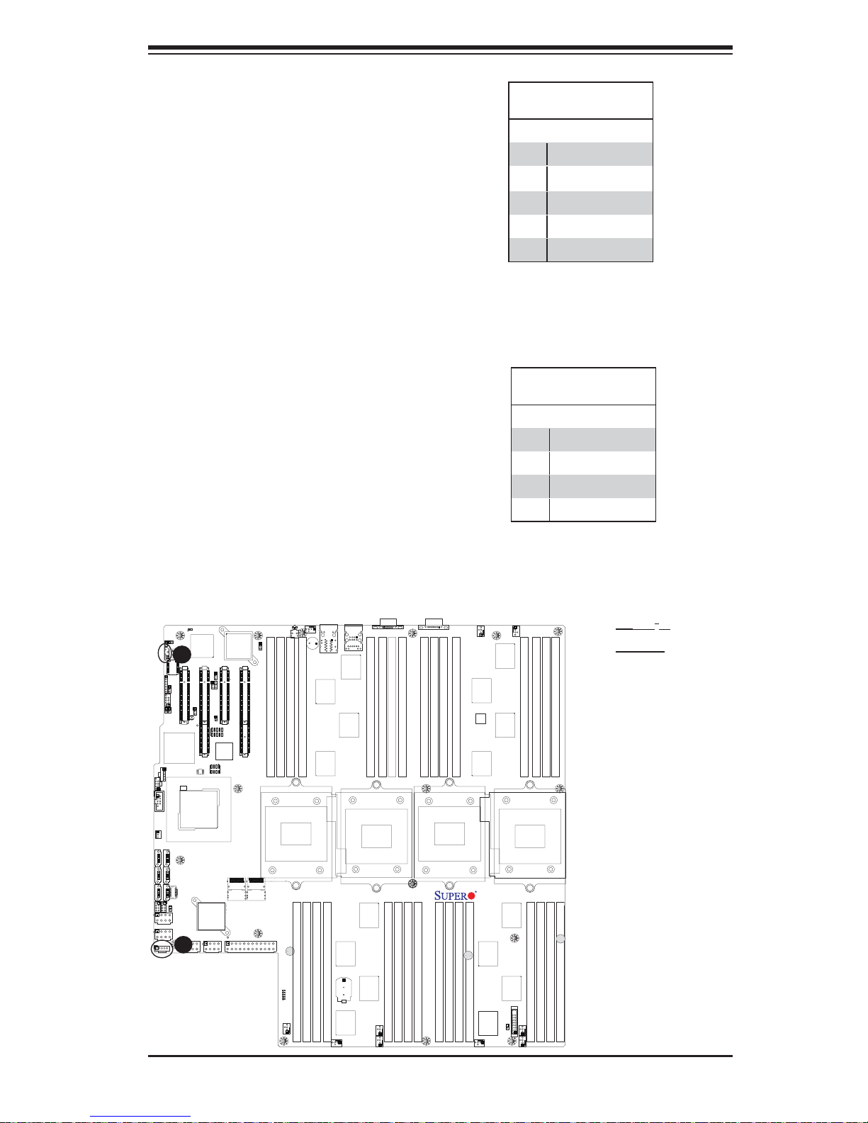
Chapter 3: Installation
5
Power SMB (I2C) Connector
Power System Management Bus (I
Connector (JPI
2
C) monitors power
2
C)
supply, fan and system temperatures.
See the table on the right for pin
defi nitions.
IPMB
A System Management Bus header for
IPMI 2.0 is located at IPMB. Connect
the appropriate cable here to use the
IPMB I
2
C connection on your system.
PWR SMB
Pin Defi nitions
Pin# Defi nition
1 Clock
2 Data
3 PWR Fail
4 Ground
5 +3.3V
IPMB Header
Pin Defi nitions
Pin# Defi nition
1 Data
2 Ground
3 Clock
4 No Connection
USB2/3
COM2
I-SATA0
I-SATA2
I-SATA4
JP6
I-SATA5
JPWR5
JPWR4
JPRST1
JWOR
IPMB
BMCRST
J40
JP4
U101
JD1
JWD1
JLPC1
JP10
PORT80
1
J35
Intel ICH 10R
USB5
FAN 11
I-SATA1
I-SATA3
J59
JP5
JL1
JPI2C1
D10
B
BBU
A
BMC_HB
Winbond
BMC CTRL
JPS1
Slot2 PCI-E 2.0 X16/X8
Slot1 PCI-E 2.0 X8
JPT1
JUID_OW1
JPB1
JBT1
U70
BIOS
Intel
IOH 7500
LSI 2108
SAS CTRL
JPWR1JPWR2
JPG1
JP3
JP1
Intel 82576
LAN CTRL
Slot4 PCI-E 2.0 X16/X8
Slot3 PCI-E 2.0 X8
SAS0~3
SAS4~7
JPWR3
UID_SWITCH
JPL1
P1-DIMM4A
P5V_STBY
UID_LED
JUIDB1
P1-DIMM3A
LED5
LED6
FAN7
LED26
P1-DIMM2A
CPU1
LED7
LED8
LED9
FAN10
P1-DIMM1A
P2-DIMM7A
P2-DIMM8A
SP1
P2-DIMM6A
LAN1
(LOWER)
LAN2
(UPPER)
P2-DIMM5A
FAN6
BT2
Battery
USB0/1
IPMI_LAN
P1-DIMM5A
P1-DIMM6A
CPU2
FAN4
FAN
VGA
P1-DIMM7A
P2-DIMM1A
P1-DIMM8A
P2-DIMM2A
P2-DIMM3A
COM1
P3-DIMM4A
P2-DIMM4A
P3-DIMM2A
P3-DIMM3A
P4-DIMM8A
P3-DIMM1A
CPU3
P4-DIMM7A
P4-DIMM6A
P4-DIMM5A
FAN9
X8QBE-F
Rev. 1.11
FAN3
FAN8
JF1
OHLED
JOH1
P3-DIMM5A
CPU4
P4-DIMM1A
FAN1
FAN2
P3-DIMM6A
P3-DIMM7A
P4-DIMM2A
P3-DIMM8A
P4-DIMM4A
P4-DIMM3A
A. JPI
B. IPMB
2
C
3-25
Page 52
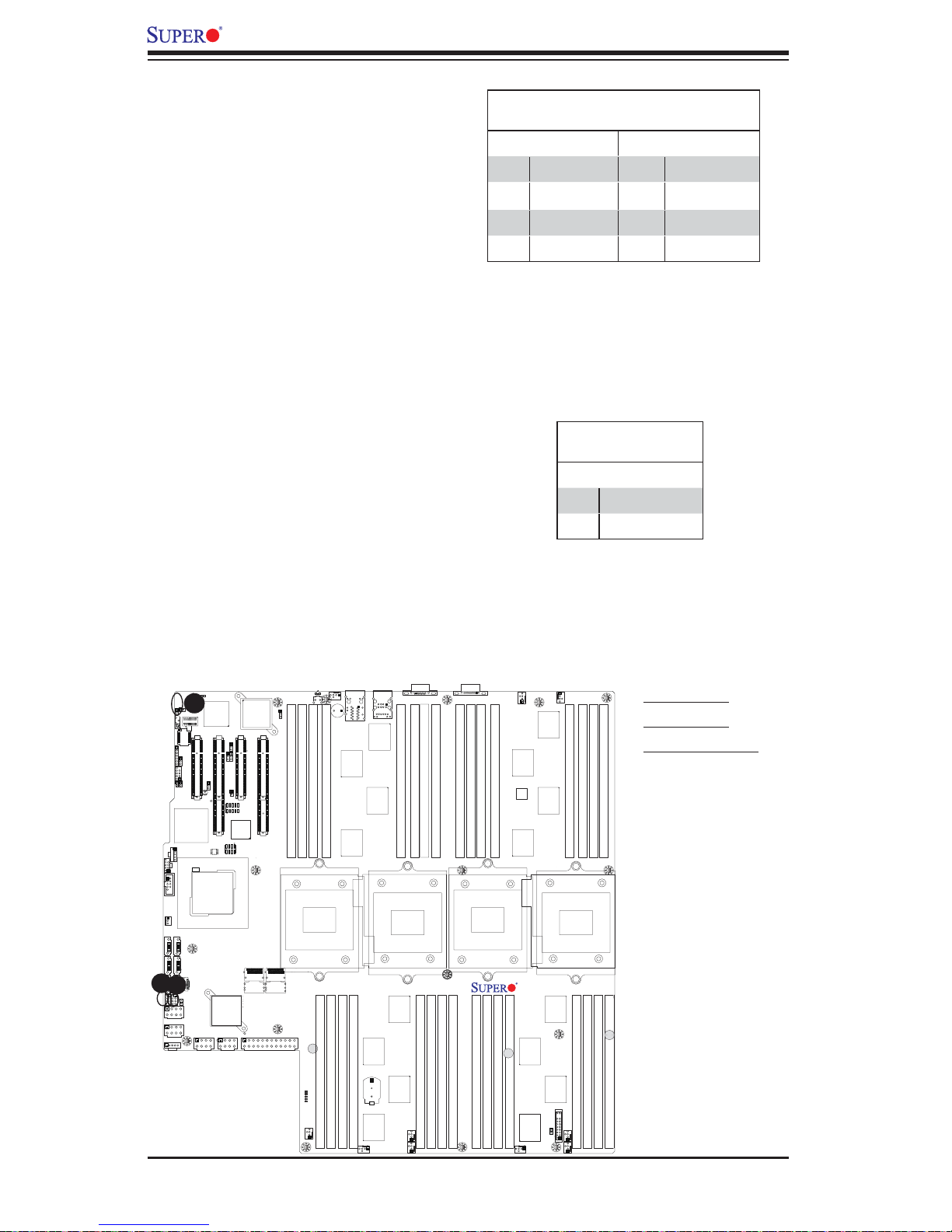
X8QB6-F/X8QBE-F Motherboard User's Manual
5
T-SGPIO 1/2 Headers
Two SGPIO (Serial-Link General
Purpose Input/Output) headers are
located on the motherboard. These
headers support Serial_Link interface
for onboard SATA connections. See
the table on the right for pin defi ni-
tions.
Wake-On-Ring
The Wake-On-Ring header is located
at JWOR. This function allows your
computer to wake up when receiving
an incoming call to the modem while
in the suspend state. See the table
on the right for pin defi nitions. You
must have a Wake-On-Ring card and
a cable to use this feature.
T-SGPIO
Pin Defi nitions
Pin# Defi nition Pin Defi nition
1NC 2 NC
3 Ground 4 Data
5 Load 6 Ground
7 Clock 8 NC
Note: NC= No Connection
Wake-On-Ring
Pin Defi nitions
Pin# Defi nition
1 Ground
2 Wake-up
USB0/1
JPRST1
JWOR
BMC_HB
D10
C
IPMB
Winbond
BMCRST
J40
BMC CTRL
JP4
U101
JD1
JWD1
JP10
1
J35
Intel ICH 10R
USB5
USB2/3
COM2
FAN 11
I-SATA1
I-SATA0
I-SATA3
I-SATA2
I-SATA5
I-SATA4
J59
B
A
JP6
JP5
JL1
JPWR5
JPWR4
JPI2C1
JLPC1
PORT80
BBU
JPS1
Slot2 PCI-E 2.0 X16/X8
Slot1 PCI-E 2.0 X8
JPT1
JPG1
JUID_OW1
JPB1
JBT1
U70
BIOS
Intel
IOH 7500
LSI 2108
SAS CTRL
JPWR1JPWR2
Intel 82576
LAN CTRL
Slot3 PCI-E 2.0 X8
JP3
JP1
SAS0~3
JPWR3
JPL1
Slot4 PCI-E 2.0 X16/X8
SAS4~7
UID_LED
JUIDB1
UID_SWITCH
P1-DIMM3A
P1-DIMM4A
LED5
P5V_STBY
LED6
FAN7
P1-DIMM2A
CPU1
LED7
LED8
LED9
FAN10
P1-DIMM1A
P2-DIMM7A
P2-DIMM8A
SP1
(LOWER)
LAN2
(UPPER)
P2-DIMM6A
P2-DIMM5A
BT2
Battery
FAN6
LAN1
LED26
IPMI_LAN
P1-DIMM5A
P1-DIMM6A
CPU2
FAN4
FAN
VGA
P1-DIMM7A
P2-DIMM2A
P2-DIMM1A
P1-DIMM8A
P2-DIMM3A
COM1
P3-DIMM4A
P2-DIMM4A
P3-DIMM2A
P3-DIMM3A
CPU3
P4-DIMM8A
P3-DIMM1A
P4-DIMM6A
P4-DIMM7A
FAN9
X8QBE-F
Rev. 1.11
P4-DIMM5A
FAN3
FAN8
JF1
OHLED
JOH1
P3-DIMM5A
CPU4
P4-DIMM1A
FAN1
FAN2
P3-DIMM6A
P3-DIMM7A
P4-DIMM2A
P3-DIMM8A
P4-DIMM4A
P4-DIMM3A
A. T-SGPIO1
B. T-SGPIO2
C. Wake-On-Ring
3-26
Page 53
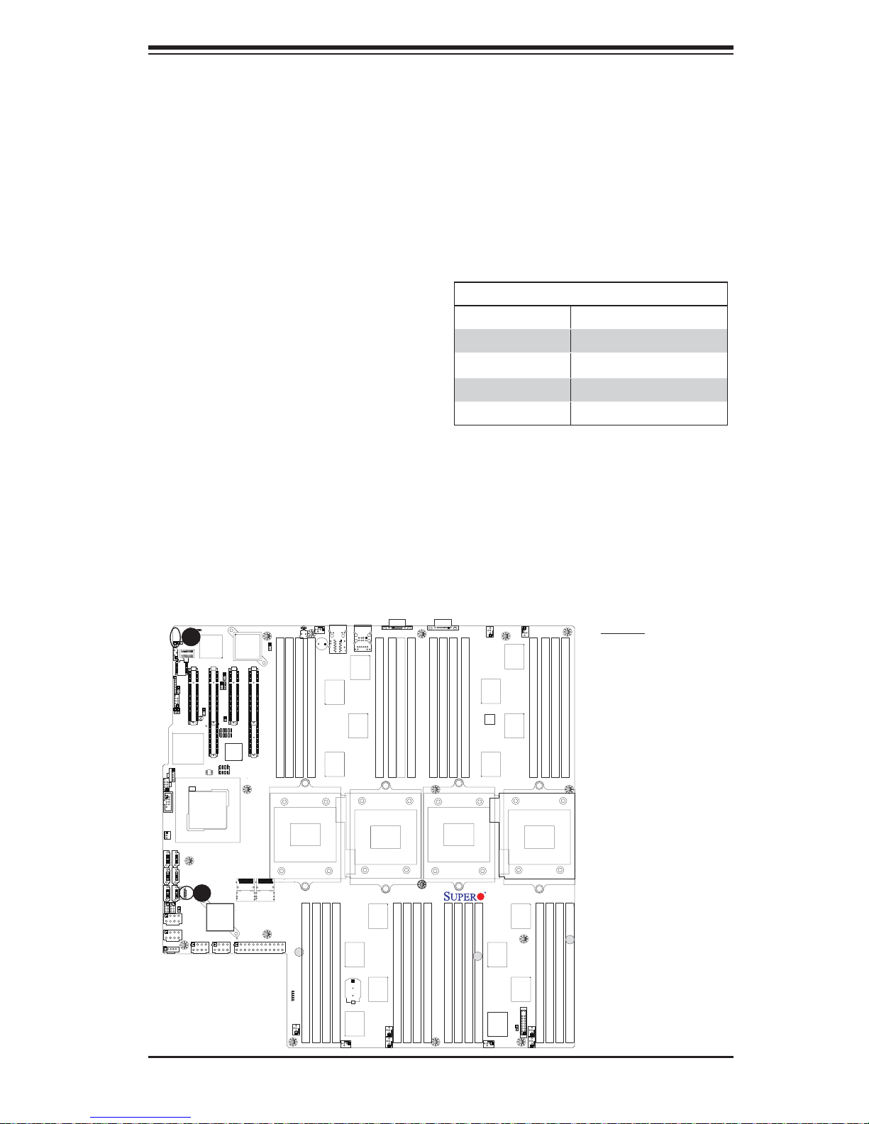
Chapter 3: Installation
5
BBU Header (Optional for the X8QB6-F Only)
A Battery-Backup Unit (BBU) header is located at J59 on the X8QB6-F. When
enabled, the BBU provides extended battery backup support for onboard SAS to
prevent data loss due to a battery 'power shortage.' To enable extended battery
support, an optional battery backup accessory kit is required. Please contact our
sales at Supermicro to purchase an LSI 2108 SAS Battery Backup Accessory kit.
Also, contact our tech support for installation instructions and possible component
updates.
LSI 2108 SAS Battery Backup Accessory Kit
Item Part Number
iBBU07 Battery BTR-0018L-0000-LSI
BBU Adaptor BTR-0018L-ADPT
Extension Cable CBL-0420L
BBU Bracket MCP-240-00094-0N
USB2/3
COM2
I-SATA0
I-SATA2
I-SATA4
JP6
JWOR
J40
JP4
FAN 11
I-SATA5
JPWR5
JPWR4
JPRST1
D10
C
IPMB
BMCRST
U101
JD1
JWD1
JLPC1
JP10
PORT80
1
J35
Intel ICH 10R
USB5
I-SATA1
I-SATA3
J59
BBU
JP5
JL1
JPI2C1
BMC_HB
Winbond
BMC CTRL
Slot2 PCI-E 2.0 X16/X8
Slot1 PCI-E 2.0 X8
JPB1
JBT1
U70
BIOS
Intel
IOH 7500
A
LSI 2108
SAS CTRL
JPWR1JPWR2
JPS1
JPT1
JPG1
JUID_OW1
Intel 82576
LAN CTRL
Slot3 PCI-E 2.0 X8
JP3
JP1
SAS0~3
JPWR3
UID_LED
JUIDB1
UID_SWITCH
JPL1
Slot4 PCI-E 2.0 X16/X8
P1-DIMM3A
P1-DIMM4A
SAS4~7
P5V_STBY
LED5
LED6
FAN7
LED26
P1-DIMM2A
CPU1
LED7
LED8
LED9
FAN10
P1-DIMM1A
P2-DIMM7A
P2-DIMM8A
SP1
P2-DIMM6A
LAN1
(LOWER)
LAN2
(UPPER)
P2-DIMM5A
USB0/1
VGA
IPMI_LAN
P1-DIMM5A
P1-DIMM6A
CPU2
BT2
Battery
FAN4
FAN
FAN6
P1-DIMM7A
P2-DIMM2A
P2-DIMM1A
P1-DIMM8A
P2-DIMM3A
COM1
P3-DIMM4A
P2-DIMM4A
P3-DIMM2A
P3-DIMM3A
CPU3
P4-DIMM8A
P3-DIMM1A
P4-DIMM6A
P4-DIMM7A
FAN9
X8QBE-F
Rev. 1.11
P4-DIMM5A
FAN3
FAN8
JF1
OHLED
JOH1
P3-DIMM5A
CPU4
P4-DIMM1A
FAN1
FAN2
P3-DIMM6A
P3-DIMM7A
P4-DIMM2A
P3-DIMM8A
P4-DIMM4A
P4-DIMM3A
A. BBU
3-27
Page 54
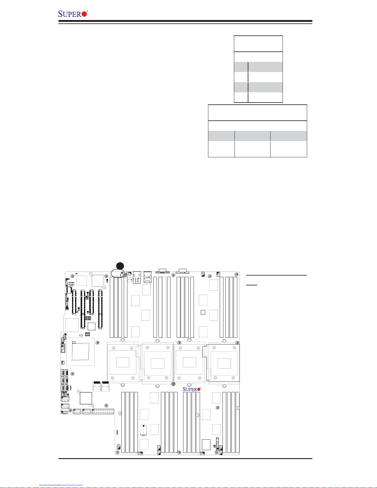
X8QB6-F/X8QBE-F Motherboard User's Manual
5
Unit Identifi cation Switch/LED
A Unit Identifi er switch (UID) and a rear UID
LED indicator (LED26) are located next to
Fan10 on the back of the chassis. When
the user pushes the rear UID switch, the
rear UID LED (LED26) will be turned on.
Push the UID switch again to turn off the
LED indicator. The UID switch provides easy
identifi cation of a system unit that may be in
need of service. See the tables on the right
for more information.
UID Switch (UID)
Pin Defi nitions
Pin# Defi nition
1 Ground
2 Ground
3 Button In
4 Ground
UID LED (LE11)
Status
Color/State OS Status
Blue: On Windows OS Unit Identifi ed
Blue:
Linux OS Unit Identifi ed
Blinking
USB2/3
COM2
I-SATA0
I-SATA2
I-SATA4
JP6
J40
FAN 11
I-SATA5
JPWR5
JPWR4
JPRST1
JWOR
IPMB
BMCRST
JP4
U101
JD1
JWD1
JLPC1
JP10
PORT80
1
J35
Intel ICH 10R
USB5
I-SATA1
I-SATA3
J59
JP5
JL1
JPI2C1
D10
BMC CTRL
Slot1 PCI-E 2.0 X8
JPB1
JBT1
Intel
IOH 7500
BBU
BMC_HB
Winbond
Intel 82576
LAN CTRL
JPS1
Slot2 PCI-E 2.0 X16/X8
JPT1
JPG1
JUID_OW1
JP3
U70
JP1
BIOS
LSI 2108
SAS CTRL
JPWR1JPWR2
Slot4 PCI-E 2.0 X16/X8
Slot3 PCI-E 2.0 X8
SAS0~3
SAS4~7
JPWR3
UID_SWITCH
JPL1
P1-DIMM4A
P5V_STBY
UID_LED
JUIDB1
A
LED26
P1-DIMM3A
P1-DIMM2A
LED5
LED7
LED8
LED9
LED6
FAN7
CPU1
P2-DIMM8A
FAN10
SP1
P1-DIMM1A
P2-DIMM7A
LAN1
(LOWER)
LAN2
(UPPER)
P2-DIMM6A
P2-DIMM5A
FAN6
Battery
BT2
USB0/1
IPMI_LAN
P1-DIMM5A
CPU2
FAN4
FAN
VGA
P1-DIMM6A
P1-DIMM7A
P2-DIMM1A
P1-DIMM8A
P2-DIMM2A
P2-DIMM3A
COM1
P3-DIMM4A
P2-DIMM4A
P3-DIMM2A
P3-DIMM3A
P4-DIMM8A
P3-DIMM1A
CPU3
P4-DIMM7A
P4-DIMM6A
P4-DIMM5A
FAN9
X8QBE-F
Rev. 1.11
FAN3
FAN8
JF1
OHLED
JOH1
P3-DIMM5A
CPU4
P4-DIMM1A
FAN1
FAN2
P3-DIMM6A
P3-DIMM7A
P4-DIMM2A
A. UID Switch & UID
LED
P3-DIMM8A
P4-DIMM4A
P4-DIMM3A
3-28
Page 55
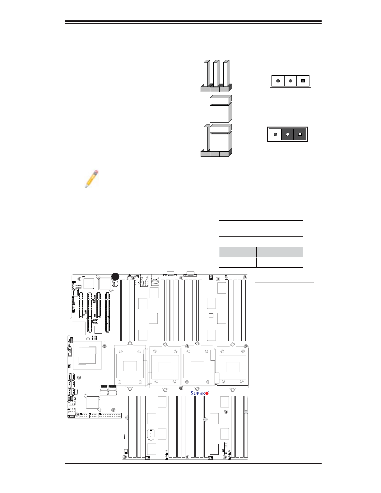
5
3-7 Jumper Settings
Connector
Pins
Jumper
Cap
Setting
Chapter 3: Installation
Explanation of Jumpers
To modify the operation of the motherboard, jumpers can be used to choose
between optional settings. Jumpers create shorts between two pins to change
the function of the connector. Pin 1
is identifi ed with a square solder pad
on the printed circuit board. See the
motherboard layout pages for jumper
locations.
Note: On two pin jumpers,
"Closed" means the jumper
is on and "Open" means the
jumper i s of f the pin s.
GLAN Enable/Disable
JPL1 enables or disables the GLAN
Port1/GLAN Port2 on the motherboard. See the table on the right for
jumper s ettings. The d efault settin g is
USB2/3
COM2
I-SATA0
I-SATA2
I-SATA4
JP6
I-SATA5
JPWR5
JPWR4
JPRST1
JWOR
IPMB
BMCRST
J40
JP4
U101
JD1
JWD1
JLPC1
JP10
PORT80
1
J35
Intel ICH 10R
USB5
FAN 11
I-SATA1
I-SATA3
J59
JP5
JL1
JPI2C1
Enabled.
BMC_HB
D10
Winbond
BMC CTRL
JPS1
Slot2 PCI-E 2.0 X16/X8
Slot1 PCI-E 2.0 X8
JPT1
JPG1
JUID_OW1
JPB1
JBT1
JP3
U70
JP1
BIOS
Intel
IOH 7500
BBU
LSI 2108
SAS CTRL
JPWR1JPWR2
Intel 82576
LAN CTRL
Slot4 PCI-E 2.0 X16/X8
Slot3 PCI-E 2.0 X8
SAS0~3
SAS4~7
JPWR3
A
UID_SWITCH
JPL1
P1-DIMM4A
P5V_STBY
UID_LED
JUIDB1
P1-DIMM3A
LED5
LED6
FAN7
LED26
P1-DIMM2A
CPU1
LED7
LED8
LED9
P1-DIMM1A
P2-DIMM8A
FAN10
SP1
P2-DIMM6A
P2-DIMM7A
LAN1
(LOWER)
LAN2
(UPPER)
P2-DIMM5A
FAN6
BT2
Battery
USB0/1
IPMI_LAN
P1-DIMM5A
P1-DIMM6A
CPU2
FAN4
FAN
VGA
P2-DIMM1A
P1-DIMM7A
P1-DIMM8A
P2-DIMM2A
P2-DIMM4A
P2-DIMM3A
COM1
P3-DIMM4A
P3-DIMM3A
P3-DIMM2A
CPU3
P4-DIMM8A
P4-DIMM7A
P3-DIMM1A
P4-DIMM6A
GLAN Enable
Jumper Settings
Jumper Setting Defi nition
1-2 Enabled (default)
2-3 Disabled
FAN8
FAN9
X8QBE-F
Rev. 1.11
P4-DIMM5A
FAN3
JF1
OHLED
JOH1
P3-DIMM5A
CPU4
P4-DIMM1A
FAN1
FAN2
P3-DIMM6A
A. GLAN Ports Enable
P3-DIMM8A
P3-DIMM7A
P4-DIMM4A
P4-DIMM3A
P4-DIMM2A
3 2 1
3 2 1
Pin 1-2 short
3-29
Page 56
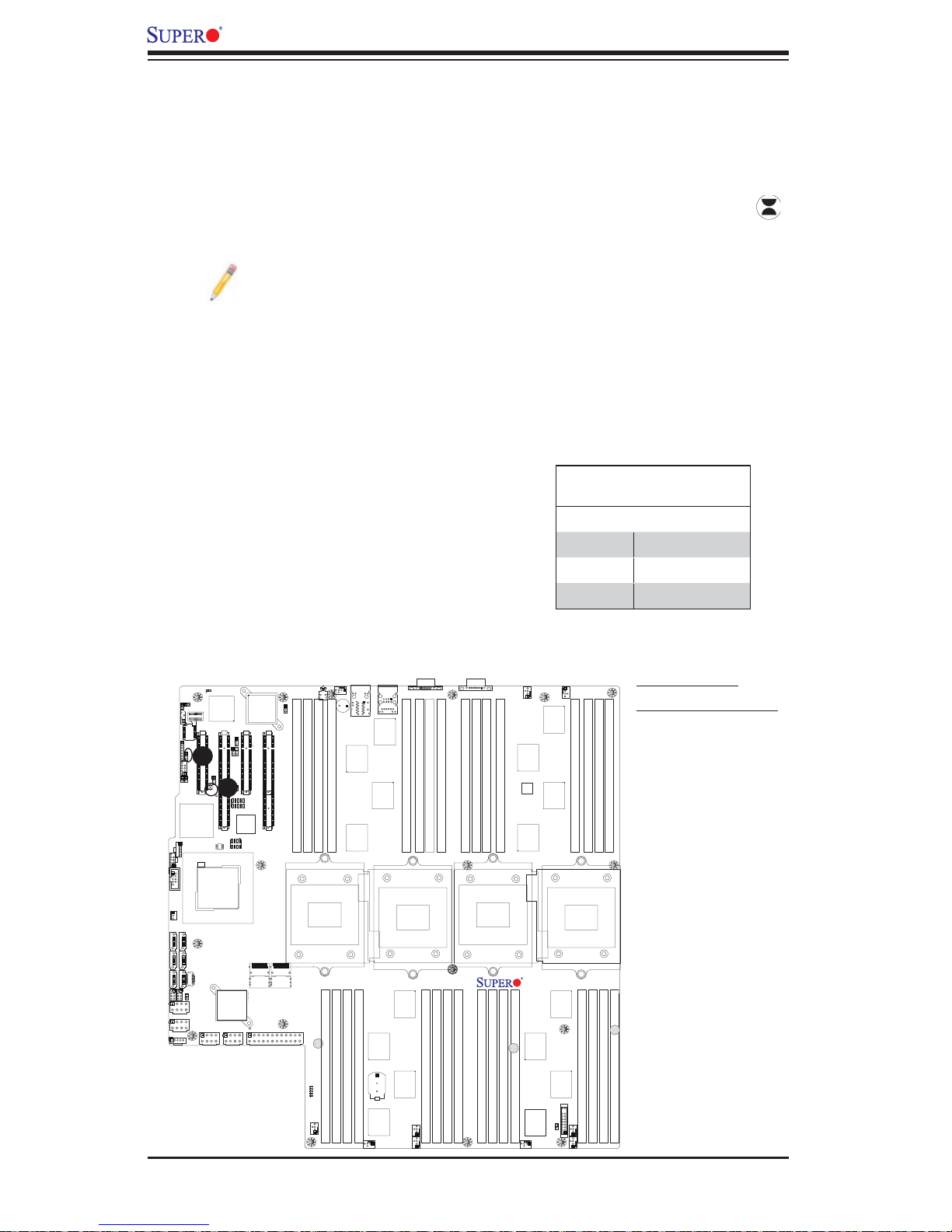
X8QB6-F/X8QBE-F Motherboard User's Manual
5
CMOS Clear
JBT1 is used to clear CMOS. Instead of pins, this "jumper" consists of contact pads
to prevent acc i d ent a l c le ar i ng o f C M OS . To clear CM O S, u se a m et al o bj e c t suc h
as a small screwdriver to touch both pads at the same time to short the connection.
Always remove the AC power cord from the system before clearing CMOS.
Note 1. For an ATX power supply, you must completely shut down the system, remove the AC power cord, and then short JBT1 to clear CMOS.
Note 2. Be sure to remove the onboard CMOS Battery before you short
JBT1 to clear CMOS.
Note 3. Clearing CMOS will also clear all passwords.
Watch Dog Enable/Disable
Watch Dog (JWD1) is a system moni to r t h at
can reb oot t he sys tem w hen a s of tware applicat ion han gs. Clo se Pins 1-2 to res et the
system if an app lication ha ngs. Close Pins
2-3 to generate a non-maskable interrupt
signal for the application that hangs. See the
Jumper Setting Defi nition
Pins 1-2 Reset (default)
Pins 2-3 NMI
Open Disabled
Watch Dog
Jumper Settings
table on the right for jumper settings. Watch
Dog must also be enabled in the BIOS.
USB2/3
COM2
I-SATA0
I-SATA2
I-SATA4
JP6
I-SATA5
JPWR5
JPWR4
JPRST1
JWOR
IPMB
BMCRST
J40
JP4
U101
JD1
JWD1
JLPC1
JP10
PORT80
1
J35
Intel ICH 10R
USB5
FAN 11
I-SATA1
I-SATA3
J59
JP5
JL1
JPI2C1
D10
B
JBT1
BBU
BMC CTRL
Slot1 PCI-E 2.0 X8
JPB1
Intel
IOH 7500
BMC_HB
Winbond
JPS1
Slot2 PCI-E 2.0 X16/X8
JPT1
JPG1
JUID_OW1
A
U70
JP1
BIOS
LSI 2108
SAS CTRL
JPWR1JPWR2
Intel 82576
LAN CTRL
Slot3 PCI-E 2.0 X8
JP3
SAS0~3
JPWR3
UID_LED
JUIDB1
UID_SWITCH
JPL1
Slot4 PCI-E 2.0 X16/X8
P1-DIMM3A
P1-DIMM4A
SAS4~7
LED5
P5V_STBY
LED6
LED7
LED8
LED9
FAN7
LED26
P1-DIMM1A
P1-DIMM2A
CPU1
P2-DIMM8A
FAN10
SP1
P2-DIMM6A
P2-DIMM7A
LAN1
(LOWER)
LAN2
(UPPER)
P2-DIMM5A
FAN6
BT2
Battery
USB0/1
IPMI_LAN
P1-DIMM5A
P1-DIMM6A
CPU2
FAN4
FAN
VGA
P1-DIMM7A
P2-DIMM1A
P1-DIMM8A
P2-DIMM2A
P2-DIMM3A
COM1
P3-DIMM4A
P2-DIMM4A
P3-DIMM2A
P3-DIMM3A
P4-DIMM8A
P3-DIMM1A
CPU3
P4-DIMM7A
P4-DIMM6A
P4-DIMM5A
FAN9
X8QBE-F
Rev. 1.11
FAN3
FAN8
JF1
OHLED
JOH1
P3-DIMM5A
CPU4
P4-DIMM1A
FAN1
FAN2
P3-DIMM6A
P3-DIMM7A
P4-DIMM2A
A. Clear CMOS
B. Watch Dog Enable
P3-DIMM8A
P4-DIMM4A
P4-DIMM3A
3-30
Page 57
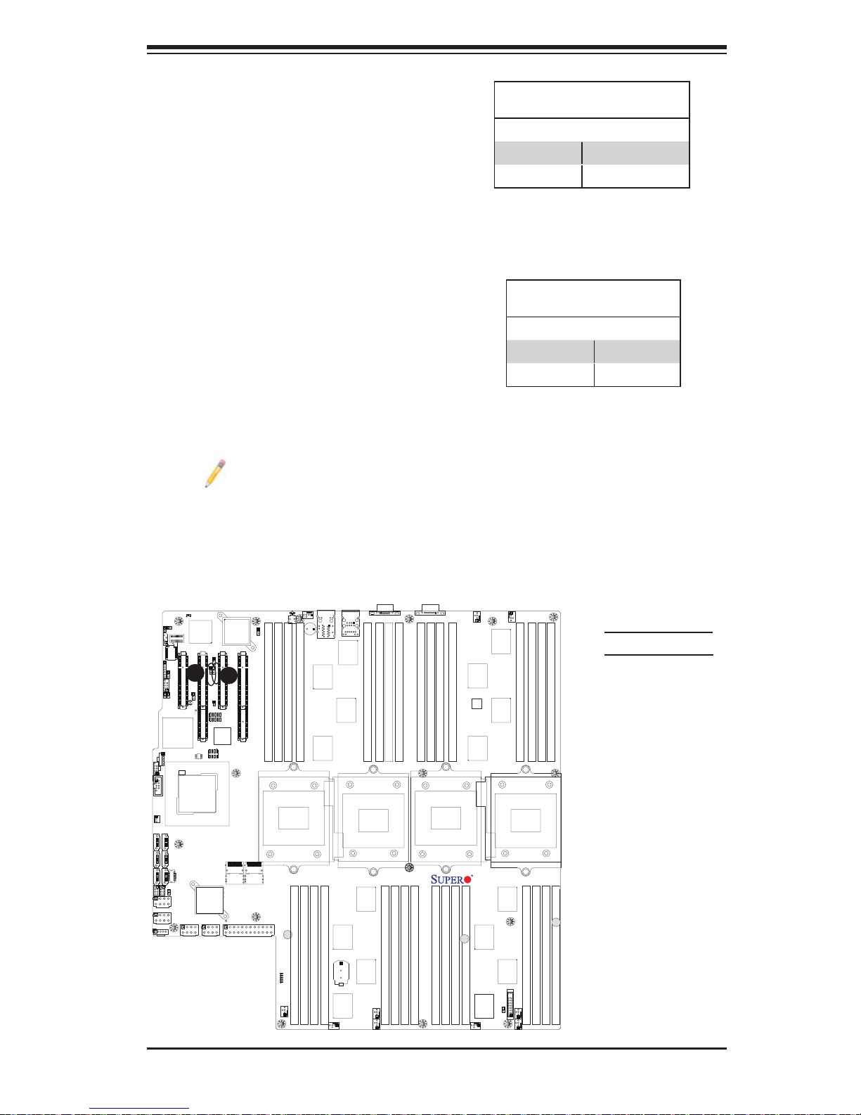
Chapter 3: Installation
5
VGA Enable
Jumper JPG1 allows the user to enable the onboard VGA connectors. The
default setting is 1-2 to enable the connection. See the table on the right for
jumper settings.
TPM Support Enable
JPT1 allows the user to enable TPM
(Trusted Platform Modules) support
to enhance data integrity and system
security. See the table on the right for
jumper settings. The default setting is
enabled.
Note: For more information on IPMI confi guration, please refer to the
WPCM 450 IPMI BMC User's Guide posted on our website @ http://www.
supermicro.com.
VGA Enable
Jumper Settings
Jumper Setting Defi nition
1-2 Enabled (Default)
2-3 Disabled
TPM Support Enable
Jumper Settings
Jumper Setting Defi nition
1-2 Enabled
2-3 Disabled
USB2/3
COM2
I-SATA0
I-SATA2
I-SATA4
JP6
I-SATA5
JPWR5
JPWR4
JPRST1
JWOR
IPMB
BMCRST
J40
JP4
U101
JD1
JWD1
JLPC1
JP10
PORT80
1
J35
Intel ICH 10R
USB5
FAN 11
I-SATA1
I-SATA3
J59
JP5
JL1
JPI2C1
D10
JBT1
BBU
BMC CTRL
Slot1 PCI-E 2.0 X8
B
JPB1
Intel
IOH 7500
BMC_HB
Winbond
JPS1
Slot2 PCI-E 2.0 X16/X8
JPT1
JPG1
JUID_OW1
U70
JP1
BIOS
LSI 2108
SAS CTRL
JPWR1JPWR2
Intel 82576
LAN CTRL
Slot3 PCI-E 2.0 X8
A
JP3
SAS0~3
JPWR3
UID_LED
JUIDB1
UID_SWITCH
JPL1
Slot4 PCI-E 2.0 X16/X8
P1-DIMM3A
P1-DIMM4A
SAS4~7
LED5
P5V_STBY
LED6
LED7
LED8
LED9
FAN7
LED26
P1-DIMM1A
P1-DIMM2A
CPU1
P2-DIMM8A
FAN10
SP1
P2-DIMM6A
P2-DIMM7A
LAN1
(LOWER)
LAN2
(UPPER)
P2-DIMM5A
FAN6
BT2
Battery
USB0/1
IPMI_LAN
P1-DIMM5A
P1-DIMM6A
CPU2
FAN4
FAN
VGA
P1-DIMM7A
P2-DIMM1A
P1-DIMM8A
P2-DIMM2A
P2-DIMM3A
COM1
P3-DIMM4A
P2-DIMM4A
P3-DIMM2A
P3-DIMM3A
P4-DIMM8A
P3-DIMM1A
CPU3
P4-DIMM7A
P4-DIMM6A
P4-DIMM5A
FAN9
X8QBE-F
Rev. 1.11
FAN3
FAN8
JF1
OHLED
JOH1
P3-DIMM5A
CPU4
P4-DIMM1A
FAN1
FAN2
P3-DIMM6A
P3-DIMM7A
P4-DIMM2A
P3-DIMM8A
P4-DIMM4A
P4-DIMM3A
A. VGA Enabled
B. TPM Enabled
3-31
Page 58

X8QB6-F/X8QBE-F Motherboard User's Manual
5
SAS2 Enable (X8QB6-F only)
Close pins 1-2 of JPS1 to enable SAS2
(Serial_Attached_SCSI) support on the
X8QB6-F motherboard. See the table on
the right for jumper settings. The default
setting is enabled.
SAS2 Enable
Jumper Settings
Jumper Setting Defi nition
1-2 Enabled (Default)
2-3 Disabled
BMC Enable
Jumper JPB1 allows you to enable the
embedded WPCM 450 BMC (Baseboard
Management) Controller to provide IPMI
2.O/KVM support on the motherboard.
See the table on the right for jumper
settings.
USB0/1
USB2/3
COM2
I-SATA0
I-SATA2
I-SATA4
JP6
J40
FAN 11
I-SATA5
JPWR5
JPWR4
JPRST1
JWOR
IPMB
BMCRST
JP4
U101
JD1
JWD1
JLPC1
JP10
PORT80
1
J35
Intel ICH 10R
USB5
I-SATA1
I-SATA3
J59
JP5
JL1
JPI2C1
D10
BMC CTRL
Slot1 PCI-E 2.0 X8
B
JPB1
JBT1
Intel
IOH 7500
BBU
BMC_HB
Winbond
Intel 82576
LAN CTRL
A
JPS1
Slot2 PCI-E 2.0 X16/X8
JPT1
JPG1
JUID_OW1
JP3
U70
JP1
BIOS
LSI 2108
SAS CTRL
JPWR1JPWR2
Slot4 PCI-E 2.0 X16/X8
Slot3 PCI-E 2.0 X8
SAS0~3
SAS4~7
JPWR3
UID_SWITCH
JPL1
P1-DIMM4A
P5V_STBY
UID_LED
JUIDB1
LED26
P1-DIMM3A
P1-DIMM2A
LED5
LED7
LED8
LED9
LED6
FAN7
CPU1
P2-DIMM8A
FAN10
SP1
P1-DIMM1A
P2-DIMM7A
LAN1
(LOWER)
LAN2
(UPPER)
P2-DIMM6A
P2-DIMM5A
Battery
FAN6
BT2
IPMI_LAN
P1-DIMM5A
CPU2
FAN4
FAN
VGA
P1-DIMM6A
P1-DIMM7A
P2-DIMM1A
P1-DIMM8A
P2-DIMM2A
P2-DIMM3A
COM1
P3-DIMM4A
P2-DIMM4A
P3-DIMM2A
P3-DIMM3A
P4-DIMM8A
P3-DIMM1A
CPU3
P4-DIMM7A
P4-DIMM6A
P4-DIMM5A
BMC Enable
Jumper Settings
Jumper Setting Defi nition
Pins 1-2 BMC Enable
Pins 2-3 Normal (Default)
FAN8
FAN9
P3-DIMM6A
P3-DIMM8A
P3-DIMM7A
P3-DIMM5A
CPU4
X8QBE-F
Rev. 1.11
P4-DIMM4A
P4-DIMM3A
P4-DIMM1A
P4-DIMM2A
JF1
OHLED
FAN1
JOH1
FAN3
FAN2
A. SAS2 Enabled
B. BMC Enabled
3-32
Page 59
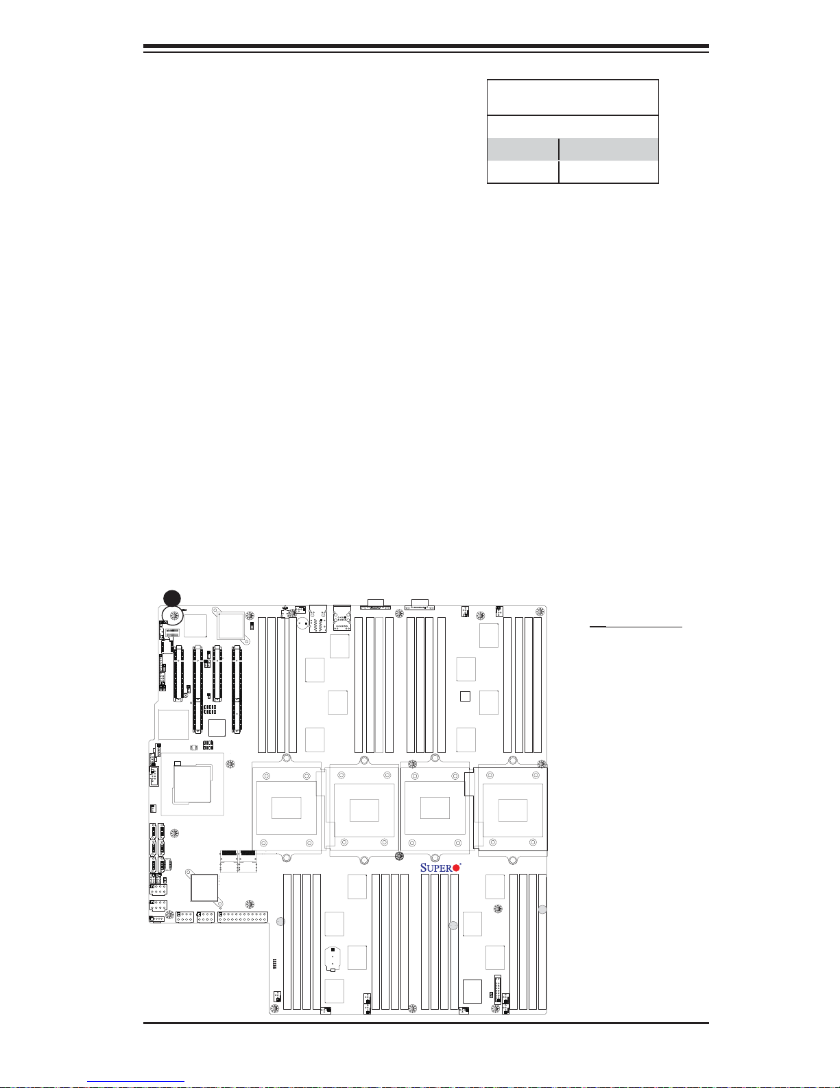
Chapter 3: Installation
5
BMC Reset
Use Jumper JPRST1 to reset the BMC
settings on the motherboard. See the
table on the right for jumper settings.
BMC Reset
Jumper Settings
Jumper Setting Defi nition
Closed BMC Reset
Closed Normal (Default)
USB2/3
COM2
I-SATA0
I-SATA2
I-SATA4
JP6
I-SATA5
JPWR5
JPWR4
A
JPRST1
JWOR
IPMB
BMCRST
J40
JP4
U101
JD1
JWD1
JLPC1
JP10
PORT80
1
J35
Intel ICH 10R
USB5
FAN 11
I-SATA1
I-SATA3
J59
JP5
JL1
JPI2C1
D10
JBT1
BBU
BMC CTRL
Slot1 PCI-E 2.0 X8
JPB1
Intel
IOH 7500
BMC_HB
Winbond
JPS1
Slot2 PCI-E 2.0 X16/X8
JPT1
JPG1
JUID_OW1
U70
JP1
BIOS
LSI 2108
SAS CTRL
JPWR1JPWR2
Intel 82576
LAN CTRL
Slot3 PCI-E 2.0 X8
JP3
SAS0~3
JPWR3
UID_LED
JUIDB1
UID_SWITCH
JPL1
Slot4 PCI-E 2.0 X16/X8
P1-DIMM3A
P1-DIMM4A
SAS4~7
LED5
P5V_STBY
LED6
LED7
LED8
LED9
FAN7
LED26
P1-DIMM1A
P1-DIMM2A
CPU1
P2-DIMM8A
FAN10
SP1
P2-DIMM6A
P2-DIMM7A
LAN1
(LOWER)
LAN2
(UPPER)
P2-DIMM5A
FAN6
BT2
Battery
USB0/1
IPMI_LAN
P1-DIMM5A
P1-DIMM6A
CPU2
FAN4
FAN
VGA
P1-DIMM7A
P2-DIMM1A
P1-DIMM8A
P2-DIMM2A
P2-DIMM3A
COM1
P3-DIMM4A
P2-DIMM4A
P3-DIMM2A
P3-DIMM3A
P4-DIMM8A
P3-DIMM1A
CPU3
P4-DIMM7A
P4-DIMM6A
P4-DIMM5A
FAN9
X8QBE-F
Rev. 1.11
FAN3
FAN8
JF1
OHLED
JOH1
P3-DIMM5A
CPU4
P4-DIMM1A
FAN1
FAN2
P3-DIMM6A
P3-DIMM7A
P4-DIMM2A
P3-DIMM8A
P4-DIMM4A
P4-DIMM3A
A. BMC Reset
3-33
Page 60
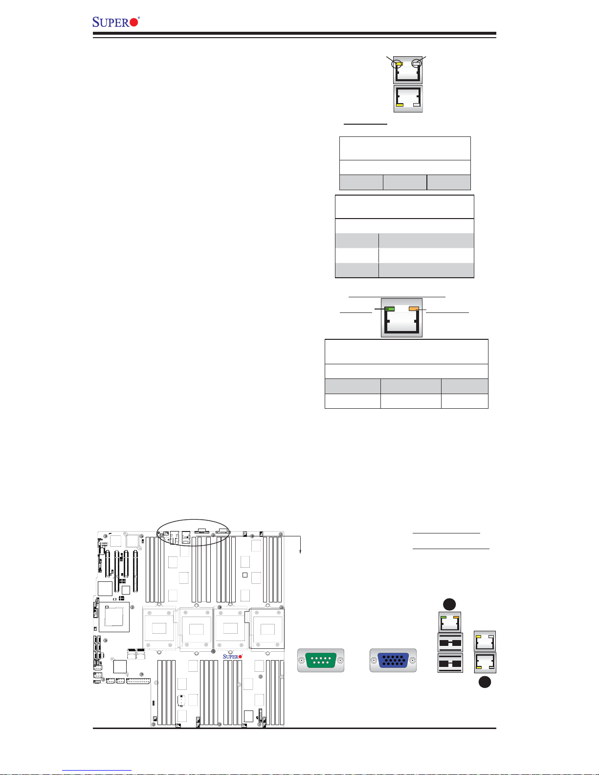
X8QB6-F/X8QBE-F Motherboard User's Manual
3-8 Onboard LED Indicators
GLAN LEDs
There are two GLAN ports on the motherboard. Each Gigabit Ethernet LAN port
has two LEDs. The Yellow (Left) LED indicates activity. The Link LED on the right
may be green, amber or off to indicate the
speed of the connection. See the tables
at right for more information.
IPMI Dedicated LAN LEDs
In addition to LAN 1/LAN 2, an IPMI
Dedicated LAN is also located on the I/O
Backplane of the motherboard. The amber
LED on the right indicates activity, while the
green LED o n the left in dicates the s peed
of the connection. See the tables at right
for more i nform ation.
Activity
LED
Link
LED
Rear View (when facing the
rear side of the chassis)
GLAN Activity Indicator (Left)
Color Status Defi nition
Yellow Flashing Active
GLAN Link Indicator (Right)
LED Color Defi nition
Off No Connection or 10 Mbps
Green 100 Mbps
Amber 1 Gbps
IPMI LAN (F models only)
Link LED Activity LED
Color/State Defi nition
Link (Left) Green: Solid 100 Mbps
Activity (Right) Amber: Blinking Active
LED Status
LED Status
IPMI LAN Link LED (Left) &
Activity LED (Right)
X8QBE-F
Rev. 1.11
A. LAN1/2 LEDs
B. IPMI LAN LEDs
B
A
3-34
Page 61
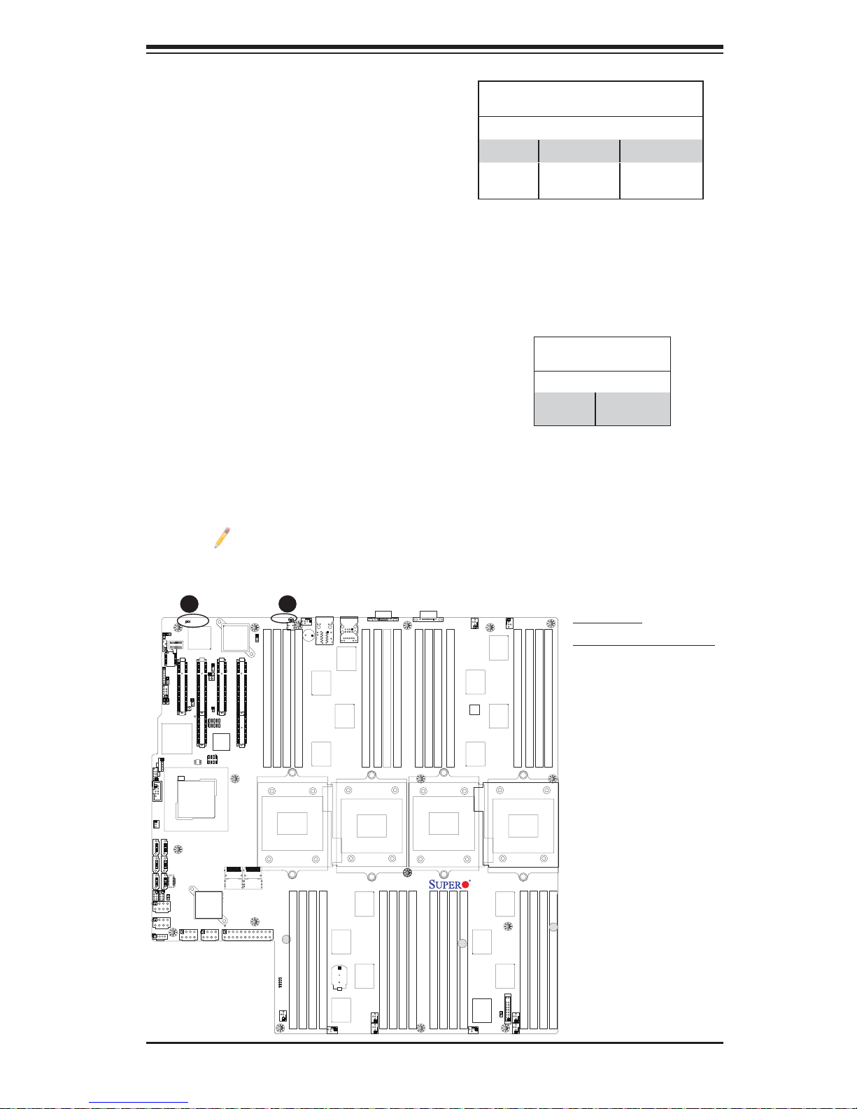
Chapter 3: Installation
5
Rear UID LED
The rear UID LED is located at LED26
on the backplane. This LED is used in
conjunction with the rear UID switch to
provide easy identifi cation of a system
that might be in need of service. Refer
to UID Switch on Page 3-15 for more
information.
BMC Heartbeat LED
A BMC He ar tbeat L ED is loc ated at D10
on the motherboard. When D10 is blinking, BMC functions normally. See the
table at r ight for m ore info rmati on.
UID LED
LED Status
Color/State OS Status
Blue: On Windows OS Unit Identifi ed
Blue:
Linux OS Unit Identifi ed
Blinking
BMC Heartbeat LED
LED Status
Color/State Defi nition
Green:
BMC: Normal
Blinking
USB2/3
COM2
I-SATA0
I-SATA2
I-SATA4
JP6
I-SATA5
JPWR5
JPWR4
JPRST1
JWOR
IPMB
BMCRST
J40
JP4
U101
JD1
JWD1
JLPC1
JP10
PORT80
1
J35
Intel ICH 10R
USB5
FAN 11
I-SATA1
I-SATA3
J59
JP5
JL1
JPI2C1
B
D10
JBT1
BBU
BMC CTRL
Slot1 PCI-E 2.0 X8
JPB1
Intel
IOH 7500
BMC_HB
Winbond
JPS1
Slot2 PCI-E 2.0 X16/X8
JPT1
JPG1
JUID_OW1
U70
JP1
BIOS
LSI 2108
SAS CTRL
JPWR1JPWR2
Note: LED Indicators that are not documented in the manual are for testing only.
Intel 82576
LAN CTRL
Slot3 PCI-E 2.0 X8
JP3
SAS0~3
JPWR3
UID_LED
JUIDB1
UID_SWITCH
JPL1
Slot4 PCI-E 2.0 X16/X8
P1-DIMM3A
P1-DIMM4A
SAS4~7
LED5
P5V_STBY
LED6
A
LED7
LED8
LED9
FAN7
LED26
P1-DIMM1A
P1-DIMM2A
CPU1
P2-DIMM8A
FAN10
SP1
P2-DIMM6A
P2-DIMM7A
LAN1
(LOWER)
LAN2
(UPPER)
P2-DIMM5A
FAN6
BT2
Battery
USB0/1
IPMI_LAN
P1-DIMM5A
P1-DIMM6A
CPU2
FAN4
FAN
VGA
P1-DIMM7A
P2-DIMM1A
P1-DIMM8A
P2-DIMM2A
P2-DIMM3A
COM1
P3-DIMM4A
P2-DIMM4A
P3-DIMM2A
P3-DIMM3A
P4-DIMM8A
P3-DIMM1A
CPU3
P4-DIMM7A
P4-DIMM6A
P4-DIMM5A
FAN9
X8QBE-F
Rev. 1.11
FAN3
FAN8
JF1
OHLED
JOH1
P3-DIMM5A
CPU4
P4-DIMM1A
FAN1
FAN2
P3-DIMM6A
P3-DIMM7A
P4-DIMM2A
A. UID LED
B. BMC Heartbeat LED
P3-DIMM8A
P4-DIMM4A
P4-DIMM3A
3-35
Page 62
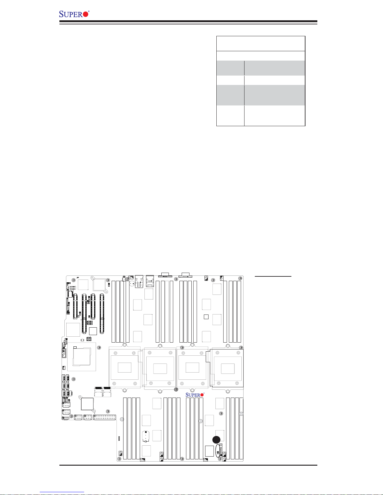
X8QB6-F/X8QBE-F Motherboard User's Manual
5
Onboard Power LED
An Onboard Power LED is located at LED
8 on the motherboard. When this LED is
on, the system is on. Be sure to turn off the
system and unplug the power cord before
removing or installing components. See
the tables at right for more information.
Onboard PWR LED Indicator
LED Status
LED Color Defi nition
Off System Off (PWR cable
not connected)
Green System On
Green:
ACPI S1 State
Flashing
Quickly
Green:
ACPI S3 (STR) State
Flashing
Slowly
USB2/3
COM2
I-SATA0
I-SATA2
I-SATA4
JP6
J40
FAN 11
I-SATA5
JPWR5
JPWR4
JPRST1
JWOR
IPMB
BMCRST
JP4
U101
JD1
JWD1
JLPC1
JP10
PORT80
1
J35
Intel ICH 10R
USB5
I-SATA1
I-SATA3
J59
JP5
JL1
JPI2C1
D10
BMC CTRL
Slot1 PCI-E 2.0 X8
JPB1
JBT1
Intel
IOH 7500
BBU
BMC_HB
Winbond
Intel 82576
LAN CTRL
JPS1
Slot2 PCI-E 2.0 X16/X8
JPT1
JPG1
JUID_OW1
JP3
U70
JP1
BIOS
LSI 2108
SAS CTRL
JPWR1JPWR2
Slot4 PCI-E 2.0 X16/X8
Slot3 PCI-E 2.0 X8
SAS0~3
SAS4~7
JPWR3
UID_SWITCH
JPL1
P1-DIMM4A
P5V_STBY
UID_LED
JUIDB1
LED26
P1-DIMM3A
P1-DIMM2A
LED5
LED7
LED8
LED9
LED6
FAN7
CPU1
P2-DIMM8A
FAN10
SP1
P1-DIMM1A
P2-DIMM7A
LAN1
(LOWER)
LAN2
(UPPER)
P2-DIMM6A
P2-DIMM5A
FAN6
Battery
BT2
USB0/1
IPMI_LAN
P1-DIMM5A
CPU2
FAN4
FAN
VGA
P1-DIMM6A
P1-DIMM7A
P2-DIMM1A
P1-DIMM8A
P2-DIMM2A
P2-DIMM3A
COM1
P3-DIMM4A
P2-DIMM4A
P3-DIMM2A
P3-DIMM3A
P4-DIMM8A
P3-DIMM1A
CPU3
P4-DIMM7A
P4-DIMM6A
P4-DIMM5A
FAN9
X8QBE-F
Rev. 1.11
A
FAN3
FAN8
JF1
OHLED
JOH1
P3-DIMM5A
CPU4
P4-DIMM1A
FAN1
FAN2
P3-DIMM6A
P3-DIMM7A
P4-DIMM2A
P3-DIMM8A
P4-DIMM4A
P4-DIMM3A
A. PWR LED
3-36
Page 63
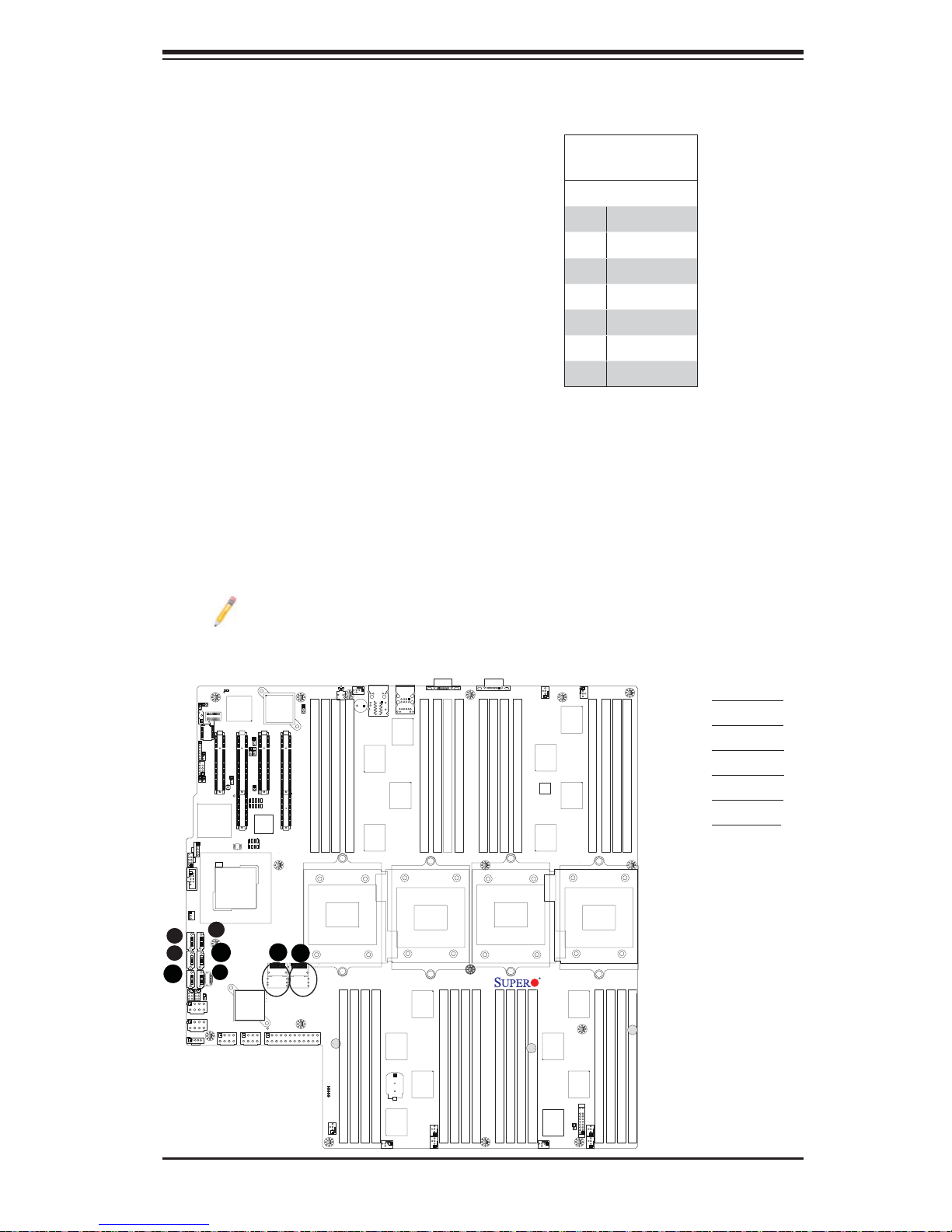
5
D
E
3-9 Serial ATA Connections
F
G
Chapter 3: Installation
Serial ATA Ports
There are six Serial ATA Ports (ISATA0~I-SATA 5) located on the
motherboard. These ports, supported by the Intel ICH10R South
Bridge, provide serial-link signal connections, which are faster than the
conn ections of Paral l e l ATA. Se e t h e
table o n the ri ght for p in defi nitions.
SAS2 Ports (X8QB6-F only)
Eight Serial_Attached_SCSI Ports
(SAS 0~3, 4~7) located on the
X8QB 6 to p r ovide serial li n k connections. T hese por ts are suppo rted by
the LSI 2108 Controller. See the table
on the r ight for p in defi nitions.
Serial ATA/SAS2
Pin Defi nitions
Pin# Defi nition
1 Ground
2 TX_P
3 TX_N
4 Ground
5 RX_N
6 RX_P
7 Ground
Note: For more information on SATA HostRAID confi guration, please refer
to the Intel SATA HostRAID User's Guide posted on our website @ http://
www.supermicro.com..
USB0/1
JPRST1
JWOR
BMC_HB
D10
IPMB
BMCRST
J40
JP4
U101
JD1
JWD1
JLPC1
JP10
PORT80
1
J35
Intel ICH 10R
USB5
USB2/3
COM2
FAN 11
I-SATA1
I-SATA0
B
A
I-SATA3
I-SATA2
C
I-SATA5
I-SATA4
J59
BBU
JP6
JP5
JL1
JPWR5
JPWR4
JPI2C1
Winbond
BMC CTRL
Slot2 PCI-E 2.0 X16/X8
Slot1 PCI-E 2.0 X8
JPT1
JUID_OW1
JPB1
JBT1
U70
BIOS
Intel
IOH 7500
LSI 2108
SAS CTRL
JPWR1JPWR2
JPS1
JPG1
JP3
JP1
Intel 82576
LAN CTRL
Slot4 PCI-E 2.0 X16/X8
Slot3 PCI-E 2.0 X8
SAS0~3
SAS4~7
JPWR3
H
UID_SWITCH
JPL1
P1-DIMM4A
P5V_STBY
UID_LED
JUIDB1
P1-DIMM3A
LED5
LED6
FAN7
P1-DIMM2A
CPU1
LED7
LED8
LED9
FAN10
P1-DIMM1A
P2-DIMM7A
P2-DIMM8A
SP1
P2-DIMM6A
(LOWER)
LAN2
(UPPER)
P2-DIMM5A
BT2
Battery
FAN6
LAN1
LED26
IPMI_LAN
P1-DIMM5A
P1-DIMM6A
CPU2
FAN4
FAN
VGA
P1-DIMM7A
P2-DIMM2A
P2-DIMM1A
P1-DIMM8A
P2-DIMM3A
COM1
P3-DIMM4A
P2-DIMM4A
P3-DIMM2A
P3-DIMM3A
P4-DIMM8A
CPU3
P4-DIMM7A
P3-DIMM1A
P4-DIMM6A
P4-DIMM5A
FAN9
X8QBE-F
Rev. 1.11
FAN3
FAN8
JF1
OHLED
JOH1
P3-DIMM5A
CPU4
P4-DIMM1A
FAN1
FAN2
P3-DIMM6A
P3-DIMM7A
P4-DIMM2A
P3-DIMM8A
P4-DIMM4A
P4-DIMM3A
A. I-SATA0
B. I-SATA1
C. I-SATA2
D. I-SATA3
E. I-SATA4
F. I-SATA5
3-37
Page 64

X8QB6-F/X8QBE-F Motherboard User's Manual
Notes
3-38
Page 65

Chapter 4: Troubleshooting
Chapter 4
Troubleshooting
4-1 Troubleshooting Procedures
Use the following procedures to troubleshoot your system. If you have followed all
of the procedures below and still need assistance, refer to the ‘Technical Support
Procedures’ and/or ‘Returning Merchandise for Service’ section(s) in this chapter.
Note: Always disconnect the power cord before adding, changing or installing any
hardware components.
Before Power On
Make sure that there are no short circuits between the motherboard and 1.
chassis.
Disconnect all ribbon/wire cables from the motherboard, including those for 2.
the keyboard and mouse.
Remove all add-on cards.3.
Install CPU 1 fi rst (-making sure it is fully seated) and connect the front panel 4.
connectors to the motherboard.
No Power
Make sure that no short circuits between the motherboard and the chassis.1.
Make sure that the ATX power connectors are properly connected2.
Check that the 115V/230V switch on the power supply is properly set, if avail-3.
able.
Turn the power switch on and off to test the system, if applicable.4.
The battery on your motherboard may be old. Check to verify that it still sup-5.
plies ~3VDC. If it does not, replace it with a new one.
4-1
Page 66

X8QB6-F/X8QBE-F Motherboard User's Manual
No Video
If the power is on, but you have no video, remove all the add-on cards and 1.
cables.
Use the speaker to determine if any beep codes exist. Refer to Appendix A 2.
for details on beep codes.
System Boot Failure
If the system does not display POST or does not respond after the power is turned
on, check the following:
Check for any error beep from the motherboard speaker. 1.
If there is no error beep, try to turn on the system without DIMM modules. If there
•
is still no error beep, try to turn on the system again with only one processor in
CPU Socket#1. If there is still no error beep, replace the motherboard.
If there are error beeps, clear the CMOS settings by unplugging the power
•
cord and contracting both pads on the CMOS Clear Jumper (JBT1). (Refer to
Section 3-7 in Chapter 3.)
Remove all components from the motherboard, especially the DIMM mod-2.
ules. Make sure that the system's power is on, and memory error beeps are
activated.
Turn on the system with only one DIMM module. If the system boots, check 3.
for bad DIMM modules or slots by following the Memory Errors Troubleshooting procedure in this Chapter.
Losing the System’s Setup Confi guration
Make sure that you are using a high quality power supply. A poor quality 1.
power supply may cause the system to lose the CMOS setup information.
Refer to Section 2-6 for details on recommended power supplies.
The battery on your motherboard may be old. Check to verify that it still sup-2.
plies ~3VDC. If it does not, replace it with a new one.
If the above steps do not fi x the Setup Confi guration problem, contact your 3.
vendor for repairs.
4-2
Page 67

Chapter 4: Troubleshooting
Memory Errors
When a No_Memory_Beep_Code is issued by the system, check the following:
Make sure that the memory modules are compatible with the system and that 1.
the DIMM modules are properly and fully installed. (For memory compatibility,
refer to the Memory Compatibility Chart posted on our Website @ http://www.
supermicro.com.)
Check if different speeds of DIMMs have been installed. It is strongly recom-2.
mended that you use the same RAM speed for all DIMMs in the system.
Make sure that you are using the correct type of DDR3 Registered ECC1066 3.
MHz SDRAM (recommended by the manufacturer).
Check for bad DIMM modules or slots by swapping a single module among 4.
all memory slots and check the results.
Make sure that all memory modules are fully seated in their slots. Follow the 5.
instructions given in Section 3-3 in Chapter 3.
Please follow the instructions given in the DIMM Population Tables listed on 6.
Page 3-8 to install your memory modules.
When the System Becomes Unstable
A. When the system becomes unstable during or after OS installation, check
the following:
CPU/BIOS support: Make sure that your CPU is supported, and you have the 1.
latest BIOS installed in your system.
Memory support: Make sure that the memory modules are supported by test-2.
ing the modules using memtest86 or a similar utility.
Note: Refer to the product page on our website http:\\www.supermicro.
com for memory and CPU support and updates.
HDD support: Make sure that all hard disk drives (HDDs) work properly. Re-3.
place the bad HDDs with good ones.
System cooling: Check system cooling to make sure that all heatsink fans, 4.
and CPU/system fans, etc., work properly. Check Hardware Monitoring settings in the BIOS to make sure that the CPU and System temperatures are
4-3
Page 68

X8QB6-F/X8QBE-F Motherboard User's Manual
within the normal range. Also check the front panel Overheat LED, and make
sure that the Overheat LED is not on.
Adequate power supply: Make sure that the power supply provides adequate 5.
power to the system. Make sure that all power connectors are connected.
Please refer to our website for more information on minimum power requirement. Also be sure to use a power supply that supports the specifi cations
listed in the table on Page 2-3 or Page 2-6.
Proper software support: Make sure that the correct drivers are used. 6.
B. When the system becomes unstable before or during OS installation, check
the following:
Source of installation: Make sure that the devices used for installation are 1.
working properly, including boot devices such as CD/DVD disc, CD/DVDROM.
Cable connection: Check to make sure that all cables are connected and 2.
working properly.
Using minimum confi guration for troubleshooting: Remove all unnecessary 3.
components (starting with add-on cards fi rst), and use minimum confi guration
(with a CPU and a memory module installed) to identify the trouble areas.
Refer to the steps listed in Section A above for proper troubleshooting procedures.
Identifying bad components by isolating them: If necessary, remove a compo-4.
nent in question from the chassis, and test it in isolation to make sure that it
works properly. Replace a bad component with a good one.
Check and change one component at a time instead of changing several 5.
items at the same time. This will help isolate and identify the problem.
To fi nd out if a component is good, swap this component with a new one to 6.
see if the system will work properly. If so, then the old component is bad.
You can also install the component in question in another system. If the new
system works, the component is good and the old system has problems.
4-2 Technical Support Procedures
Before contacting Technical Support, please take the following steps. Also, please
note that as a motherboard manufacturer, Supermicro also sells motherboards
4-4
Page 69

Chapter 4: Troubleshooting
through its channels, so it is best to fi rst check with your distributor or reseller for
troubleshooting services. They should know of any possible problem(s) with the
specifi c system confi guration that was sold to you.
Please go through the ‘Troubleshooting Procedures’ and 'Frequently Asked 1.
Question' (FAQ) sections in this chapter or see the FAQs on our website
(
http://www.supermicro.com/) before contacting Technical Support.
BIOS upgrades can be downloaded from our website 2.
com).
If you still cannot resolve the problem, include the following information when 3.
contacting Supermicro for technical support:
Motherboard model and PCB revision number
•
BIOS release date/version (This can be seen on the initial display when your •
system fi rst boots up.)
System confi guration
•
An example of a Technical Support form is on our website at 4. (http://www.
supermicro.com).
Distributors: For immediate assistance, please have your account number ready
•
when placing a call to our technical support department. We can be reached
by e-mail at [email protected].
(http://www.supermicro.
4-3 Frequently Asked Questions
Que sti on: Wh at a re th e var iou s t ype s of m emo r y th at my mo th er boa rd c an
support?
Answer: The motherboard supports Registered ECC DDR3 1066 MHz SDRAM
modules. It is strongly recommended that you do not mix memory modules of different speeds and sizes. Please follow all memory installation instructions given on
Section 3-3 in Chapter 3.
Que stio n: How do I u pda te my BI OS?
It is recommended that you do not upgrade your BIOS if you are not experiencing
any problems with your system. Updated BIOS fi les are located on our website
at
http://www.supermicro.com. Please check our BIOS warning message and the
information on how to update your BIOS on our website. Select your motherboard
model and download the BIOS fi le to your computer. Also, check the current BIOS
4-5
Page 70

X8QB6-F/X8QBE-F Motherboard User's Manual
revision to make sure that it is newer than your BIOS before downloading. You can
choose from the zip fi le and the .exe fi le. If you choose the zip BIOS fi le, please
unzip the BIOS fi le onto a bootable USB device. Run the batch fi le using the format
AMI.bat fi lename.rom from your bootable USB device to fl ash the BIOS. Then, your
system will automatically reboot.
Warning: Do not shut down or reset the system while updating the BIOS
to prevent possible system boot failure!)
Note: The SPI BIOS chip used on this motherboard cannot be removed.
Send your motherboard back to our RMA Department at Supermicro for
repair. For BIOS Recovery instructions, please refer to the AMI BIOS
Recovery Instructions posted at http://
Question: What 's on the CD that came with my motherboard?
Answer: The supplied compact disc has quite a few drivers and programs that will
greatl y enhanc e your sys tem. We rec omme nd that you r eview th e CD and in stall
the appl icat ions you n eed. Ap plic ation s on the C D inclu de chip set dri vers fo r the
Window s OS, sec uri ty and a udio dr ivers.
www.supermicro.com.
Question: H ow do I ha ndl e the u sed ba tt er y?
Answer: Please handle used batteries carefully. Do not damage the battery in any
way; a damaged battery may release hazardous materials into the environment.
Do not discard a used battery in the garbage or a public landfi ll. Please comply
with the regulations set up by your local hazardous waste management agency to
dispose of your used battery properly.
4-4 Returning Merchandise for Service
A receipt or copy of your invoice marked with the date of purchase is required before
any warranty service will be rendered. You can obtain service by calling your vendor for a Returned Merchandise Authorization (RMA) number. When returning the
motherboard to the manufacturer, the RMA number should be prominently displayed
on the outside of the shipping carton, and the shipping package is mailed prepaid
or hand-carried. Shipping and handling charges will be applied for all orders that
must be mailed when service is complete. For faster service, You can also request
a RMA authorization online (http://
This warranty only covers normal consumer use and does not cover damages incurred in shipping or from failure due to the alternation, misuse, abuse or improper
maintenance of products.
www.supermicro.com).
During the warranty period, contact your distributor fi rst for any product problems.
4-6
Page 71

Chapter 5: AMI BIOS
Chapter 5
BIOS
5-1 Introduction
This chapter describes the AMI BIOS Setup Utility for the X8QB6-F/X8QBE-F. The
AMI ROM BIOS is stored in a Flash EEPROM and can be easily updated. This chapter describes the basic navigation of the AMI BIOS Setup Utility setup screens.
Starting BIOS Setup Utility
To enter the AMI BIOS Setup Utility screens, press the <Delete> key while the
system is booting up.
Note: In most cases, the <Delete> key is used to invoke the AMI BIOS
setup screen. There are a few cases when other keys are used, such as
<F1>, <F2>, etc.
Each main BIOS menu option is described in this manual. The Main BIOS setup
menu screen has two main frames. The left frame displays all the options that can
be confi gured. Grayed-out options cannot be confi gured. Options in blue can be
confi gured by the user. The right frame displays the key legend. Above the key
legend is an area reserved for text messages. When an option is selected in the left
frame, it is highlighted in white. Often a text message will accompany it. (Note: AMI
BIOS has default text messages built in. Supermicro retains the option to include,
omit, or change any of these text messages.)
The AMI BIOS Setup Utility uses a key-based navigation system called "hot keys."
Most of the AMI BIOS setup utility "hot keys" can be used at any time during the
setup navigation process. These keys include <F1>, <F10>, <Enter>, <ESC>, arrow keys, etc.
Note: Options printed in Bold are default settings.
How To Change the Confi guration Data
The confi guration data that determines the system parameters may be changed by
entering the AMI BIOS Setup utility. This Setup utility can be accessed by pressing
<Del> at the appropriate time during system boot.
Note: For AMI BIOS Recovery, please refer to the AMI BIOS Recovery
Instructions posted on our website at http://www.supermicro.com/support/
manuals/.
5-1
Page 72
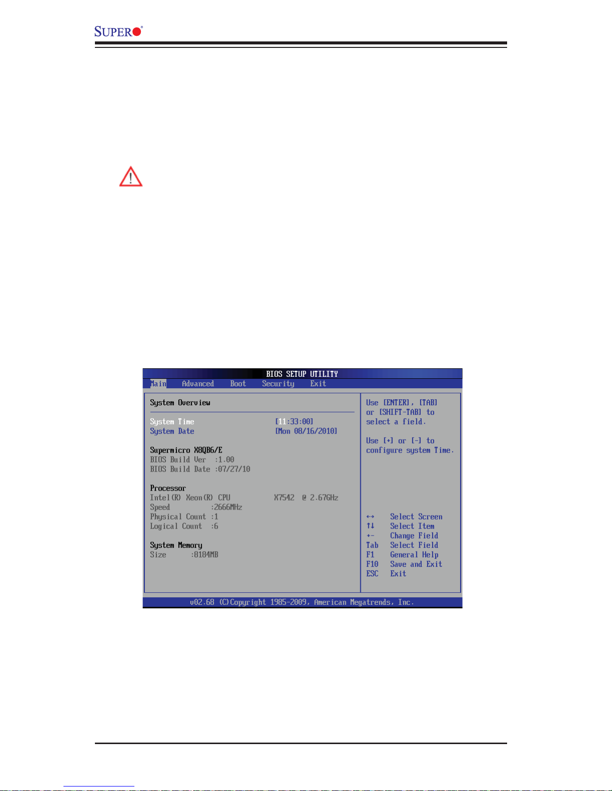
X8QB6-F/X8QBE-F Motherboard User’s Manual
Starting the Setup Utility
Normally, the only visible Power-On Self-Test (POST) routine is the memory test.
As the memory is being tested, press the <Delete> key to enter the main menu of
the AMI BIOS Setup Utility. From the main menu, you can access the other setup
screens. An AMI BIOS identifi cation string is displayed at the left bottom corner of
the screen below the copyright message.
Warning! Do not upgrade the BIOS unless your system has a BIOS-related
issue. Flashing the wrong BIOS can cause irreparable damage to the
system. In no event shall Supermicro be liable for direct, indirect, special,
incidental, or consequential damages arising from a BIOS update. If you
have to update the BIOS, do not shut down or reset the system while the
BIOS is updating to avoid possible boot failure.
5-2 Main Setup
When you fi rst enter the AMI BIOS Setup Utility , you will enter the Main setup screen.
You can always return to the Main setup screen by selecting the Main tab on the
top of the screen. The Main BIOS Setup screen is shown below.
5-2
Page 73

Chapter 5: AMI BIOS
System Overview: The following BIOS information will be displayed:
System Time/System Date
Use this option to change the system time and date. Highlight System Time or System Date using the arrow keys. Enter new values through the keyboard and press
<Enter>. Press the <Tab> key to move between fi elds. The date must be entered in
Day MM/DD/YY format. The time is entered in HH:MM:SS format. (Note: The time
is in the 24-hour format. For example, 5:30 P.M. appears as 17:30:00.)
Supermicro X8QB6/E
BIOS Version
• : This item displays the BIOS vision used in your system.
BIOS Build Date
• : This item displays the date when this BIOS was built.
Processor
The AMI BIOS will automatically display the status of the processor used in your
system:
CPU Type
• : This item displays the type of CPU used in the motherboard.
Speed
• : This item displays the CPU speed as detected by the BIOS.
Physical Count
• : This item displays the number of processors installed in your
system as detected by BIOS.
Logical Count
• : This item displays the number of CPU Cores detected in your
system by BIOS.
System Memory
Size
• : This displays the size of memory available in the system.
5-3
Page 74
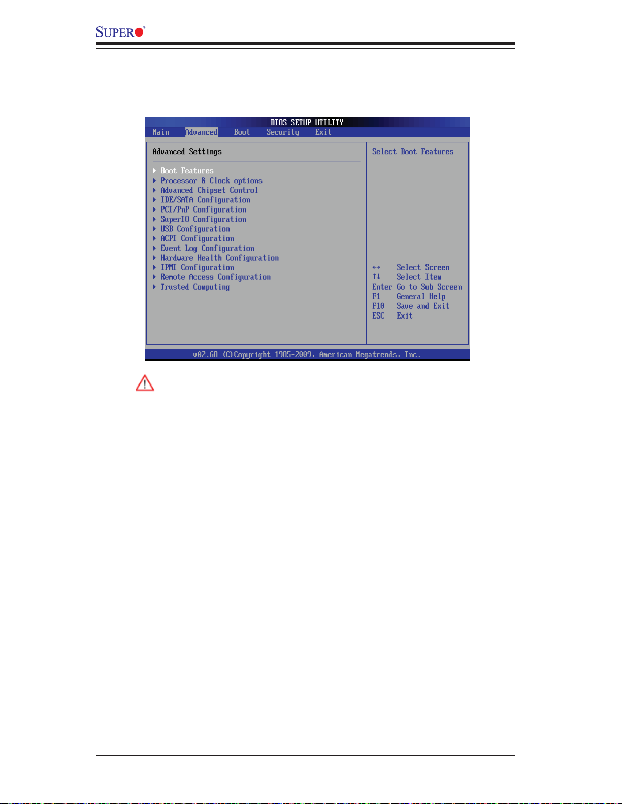
X8QB6-F/X8QBE-F Motherboard User’s Manual
5-3 Advanced Setup Confi gurations
Use the arrow keys to select Advanced Settings and press <Enter> to access the
submenu items.
Warning: Be sure to select the correct setting for each item in this section.
A wrong setting selected may cause the system to malfunction.
Boot Features
Quick Boot
If enabled, this feature will skip certain tests during POST to reduce the time needed
for system boot. The options are Enabled and Disabled.
Quiet Boot
Use this feature to select the bootup screen display between POST messages or
the OEM logo. Select Disabled to display the POST messages. Select Enabled
to display the OEM logo instead of the normal POST messages. The options are
Enabled and Disabled.
AddOn ROM Display Mode
This feature sets the display mode for the Option ROM. The options are Force
BIOS and Keep Current.
Bootup Num-Lock
This feature is used to select the Power-on state for the Numlock key. The options
are Of f and On.
5-4
Page 75

Chapter 5: AMI BIOS
PS/2 Mouse Support
Select Enabled to enable PS/2 Mouse support. Select Auto to enable the onboard
PS/2 mo use w hen a PS /2 m ouse i s detec ted. T he o ptio ns ar e Enabl e, Dis abl ed,
and Aut o.
Wait For 'F1' If Error
This for ces t he syste m to wait unti l the ' F1' key is pressed wh en an er ror o ccu rs.
The opti ons are D isab led and Enab led.
Hit 'Del' Message Display
Select Enabled to display "Press DEL to run Setup" during POST. The options
are Enabled and Disabled.
Interrupt 19 Capture
Interrupt 19 is the software interrupt that handles boot disk functions. When this item
is set to Enabled, the ROM BIOS of the host adaptors will "capture" Interrupt 19
at bootup and allow the drives that are attached to these host adaptors to function
as bootable disks. If this item is set to Disabled, the ROM BIOS of the host adaptors will not capture Interrupt 19, and the drives attached to these adaptors will not
function as bootable devices. The options are Enabled and Disabled.
Watch Dog Function
If enable d, the Watch Dog Timer w i ll allow the system to reb oot when it is inacti ve
for more t han 5 minu tes. The o ption s are Enabl ed and Disabled.
Processor and Clock Options
This submenu displays the status of the processor used in the motherboard and
allows the user to confi gure the Processor and Clock settings.
Spread Spectrum Mode
Select Enable to enable Clock Spectrum modulation support, which will allow BIOS
to monitor and attempt to reduce the level of Electromagnetic Interference caused
by the components whenever needed. The options are Disabled and Enabled.
Ratio CMOS Setting (Available when CPU Ratio is set to manual)
This option allows the user to set the ratio between the CPU Core Clock and the FSB
Frequency. (Note: if an invalid ratio is entered, the AMI BIOS will restore the setting
to the previous state.) The default setting depends on the type of CPU installed on
the motherboard. The default setting for this motherboard is [20].
5-5
Page 76

X8QB6-F/X8QBE-F Motherboard User’s Manual
Sever Class
Use this item to identify the server class for your system so that the prefectcher
settings listed below can be correctly confi gured. The options are Enterprise, HPC
(High Performance Cluster) and Custom (for customized servers).
Hardware Prefetcher (Available when supported by the CPU)
If enabled, the hardware prefetcher will prefetch streams of data and instructions
from the main memory to the L2 cache to improve CPU performance. The options
are Disabled and Enabled.
Adjacent Cache Line Prefetch (Available when supported by the CPU)
If this feature is set to Disabled, the CPU prefetches the cache line for 64 bytes. If
this feature is set to Enabled, the CPU prefetches both cache lines for 128 bytes
as comprised.
MPS and ACPI MADT Ordering
This feature allows the user to confi gure the MPS (Multi-Processor Specifi ca-
tions) and ACPI settings for your motherboard. Select Modern Ordering if XP
or a newer version of Windows OS is used in the motherboard. Select Legacy
Order i ng i f 2000 or an ear l ie r ver s io n is u se d. T he o pti o ns a re Modern Ordering
and Legacy Ordering.
Max CPUID Value Limit
This feature allows the user to set the maximum CPU ID value. Enable this feature
to boot the legacy operating systems that cannot support processors with extended
CPUID functions. The options are Enabled and Disabled (for the Windows OS).
Intel® Virtualization Technology (Available when supported by the CPU)
Select Enabled to enable Virtualization Tec hnolo gy suppor t whic h will all ow one
platf orm to r un mult iple op erati ng system s and app licat ions i n indep endent p ar titions, creating multiple "virtual" systems in one physical computer. The options are
Enabled and Dis able d. Note: If there i s any chan ge to thi s set ting, yo u will n eed
to power of f and re star t the syst em for the c hange to t ake eff ect. Pl ease refe r to
Intel’s website fo r detaile d infor mation.
Execute-Disable Bit Capability (Available when supported by the OS and
the CPU)
Select Enabled to enable the Execute Disable Bit support which will allow the processor to designate areas in the system memory where an application code can
execute and where it cannot, thus preventing a worm or a virus from fl ooding illegal
codes to overwhelm the processor or damaging the system during an attack. The
default is Enabled. (Refer to Intel and Microsoft websites for more information.)
5-6
Page 77

Chapter 5: AMI BIOS
CPU Multi-Core Enable/Disable (Available when supported by the CPU)
Select Enabled to enable multi-core CPU support to enhance CPU performance.
The options are Disabled and Enabled.
A20M
When the A20M# pin is enabled, it will force address bit 20 to zero (to be masked)
to emulate the address wraparound for the real-address mode at 1 MB. Set this
item to Enabled for the legacy operating systems and applications that require A20M
support to work properly. The options are Enabled and Disabled.
Intel® SpeedStep™ Technology
Intel EIST (Enhanced Intel SpeedStep Technology) allows the system to automatically adjust the processor voltage and core frequency in an effort to reduce power
consumption and heat dissipation. Please refer to Intel’s website for detailed information. The options are Disable (Disable GV3) and Enable (Enable GV3).
Intel® TurboMode Tech (Available when Intel EIST Technology is enabled)
Select Enabled to use the TurboMode Technique to boost system performance. The
options are Enabled and Disabled.
Performance/Walt Select
Use this feature to balance the need between system performance and energy saving. The options are Traditional and Power Optimized (for energy saving).
Intel® C-STATE Tech
If this feature is enabled, C-State is set by the system automatically to either C2, C3
or C4 state. The options are Disabled and Enabled. If this feature is set to Enabled,
the following items will display.
C-State Package Limit Setting
If this feature is set to Auto, the AMI BIOS will automatically set the limit on the
C-State package register. The options are Auto, C1, C3, C6 and C7.
C1 Auto Demotion
Select Enabled to allow the CPU to demote C3, C6, or C7 requests to C1 based on
un-core auto-demote information. The options are Disabled and Enabled.
C3 Auto Demotion
If this feature is set to Enabled, the CPU will conditionally demote C6 or C7 requests to C3 based on un-core auto-demote information. The options are Disabled
and Enabled.
5-7
Page 78

X8QB6-F/X8QBE-F Motherboard User’s Manual
ACPI T State
When this feature is enabled, CPU Throttling state will be reported in the ACPI
(Advanced Confi guration and Power Interface) protocol. The options are Enabled
and Disabled.
Advanced Chipset Control
The items included in the Advanced Settings submenu are listed below.
CPU Bridge Confi guration
QPI Confi guration
QuickPath Interconnect (QPI) is the connection between the CPU and the motherboard's I/O hub. This section displays the following QPI items.
MMConfi gBase
This item is used to select the space-based address for memory_mapped con-
fi guration. The options are 0x8000 0000, 0x4000 0000, and 0xC000 0000.
MMIOH Size Per IOH
Use this feature to select the memory_mapped IOH size to be allocated to each
IOH. The options are 2G, 4G, 6G, and 8G.
Logical Interrupt Mode
This item is used to select the logical interrupt mode. The options are Flat Mode
and Cluster Mode.
Cluster Mode Check Sampling
Select Enabled to check if the APICID in an IntPriUpd message is not zero. The
options are Enabled and Disabled.
QPI Debug Message Output Level
This feature allows the user to decide the level of an QPI debug message to
be sent to the user. The options are Err/Warn/Info0/1, Err/Warn/Info0, and Err/
Warn.
CRC Mode
Use this feature to select the QPI CRC (Cyclic Redundancy Check) mode, which
will determine how often the raw computer data stored in a network or a hard disk
device is checked for CRC. The options are 8Bit CRC and 16Bit Rolling CRC.
5-8
Page 79

Chapter 5: AMI BIOS
QPI (Quick Path Interconnect) Links Speed
Use this feature to set data transfer speed for QPI Link connections. The options
are Slow and Fast.
QPI Frequency Select (Available if the item - QPI Link Speed is set to
Fast)
This feature is used to set desired QPI frequency. The options are 4.800 GT,
5.866GT, 6.400 GT and Auto.
QPI Scrambling
Select Enabled to enable Bit-Shuffl ing support which will allow bits in the data
fl ow to be shifted around for CRC checking during data transmission and receiv-
ing between the CPUs or between a CPU and an IO hub (IOH). The options are
Enabled and Disabled.
Integrated Memory Controller Confi guration
Interleave Type
Use this feature to select memory interleaving mode. Select Inter-Socket Block
Interleaving to enable memory interleaving between blocks of memory installed
in different DIMM slots. Select Intra-Socket Block Interleaving to enable memory
interleaving between blocks of memory installed in the same DIMM slot. Select
Automatic to allow BIOS to automatically select the memory interleaving mode for
memory modules installed in the system. The options are No Interleaving, Inter-
Socket Block Interleaving, Intra-Socket Block Interleaving, and Automatic.
Interleave Order
Use this feature to set the order of memory interleaving. The options are High
Only, High Low, Low High 0, and Low High 1.
Mirroring
Mirroring support allows data stored in one location to be copied into another
location for data redundancy and security. The options are listed below:
No Mirroring
• (Mirroring Disabled),
Intra-Socket Mirrored Nx1 to Nx3 (Memory Controller 1 to Memory Controller 3
•
of the same DIMM socket),
Intra-Socket Mirrored Nx3 to Nx1 (Memory Controller 3 to Memory Controller 1
•
of the same DIMM socket),
Inter-Socket Mirrored S0 (Socket 0) to S1 (Socket 1), and S2 (Socket 2) to
•
S3 (Socket 3),
5-9
Page 80

X8QB6-F/X8QBE-F Motherboard User’s Manual
Inter-Socket Mirrored S0 (Socket 0) to S2 (Socket 2) and S1 (Socket 1) to S3 •
(Socket 3),
Inter-Socket Mirrored S0 (Socket 0) to S3 (Socket 3) and S1 (Socket 1) to S2
•
(Socket 2).
Spare Enable
Select Enabled to enable spare support for all sockets, creating a spare drive
for each socket. The options are Enabled and Disabled.
Mapper Mode
Use this feature to set the memory_mapper mode, which is used to translate local
physical addresses presented by a media device into DRAM memory addresses
(in terms of rank, bank, row and column). Select Open to maximize open_page
hits. Select Close to minimize rank confl icts and to maximize simultaneous read/
write bandwidth to boost performance. Select Adaptive to spread power dissipation over different DIMM modules to avoid memory overheat. The options are
Close, Open and Adaptive.
Frequency Limit
This feature forces a DDR3 memory module to run at a frequency other than
what the system has detected. The available options are Auto, 800 MHz, 978
MHz, 1067 MHz, and Auto.
Initialization Mode
Use this feature to select the memory initialization mode. The options are Serial
and Parallel.
Hemisphere Mode
This feature is used to set the memory hemisphere mode. Select Enabled to
prevent CPU's cache agent 1 from accessing cache agent 2 in an effort to
reduce memory latency and maximize performance. This setting requires that
both DIMM modules and DRAM sizes are confi gured in the same way. Select
Disabled to allow a CPU's cache agent 1 to access cache agent 2. The options
are Disabled and Enabled.
Page Policy
Use this feature to confi gure Page Policy settings, which determine how memory
blocks are cached in a DRAM buffer and a memory module accesses memory
resources. Select Open to optimize memory performance. Select Close to use
memory safe mode. Select Adaptive to balance safety and performance. The
options are Close, Open and Adaptive.
5-10
Page 81

Chapter 5: AMI BIOS
Scheduler Policy
Use this feature to confi gure Scheduler_Policy settings. The scheduler is used
to translate memory read/write commands into memory sub-commands for easy
execution. Select Static Trade_Off to balance read/write priority. Select Static
Read_Priority to optimize read latency and bandwidth. Select Static Write_Priority to optimize write bandwidth to expedite command writing and execution.
Select Adaptive to minimize latency. The options are Static Trade_Off, Static
Read_Priority, Static Write_Priority, and Adaptive.
ECC Check Time Interval
This feature is used to set the time interval between each ECC Memory checking.
If an ECC error occurs, an error message will also be sent via IPMI. The options
are 100 Msec, 1 Sec, 10 Sec, 1 Min, 5 Minutes, and 10 Minutes.
North Bridge Confi guration
This feature allows the user to confi gure North Bridge settings.
Relaxed Ordering
Select Enabled to enable PCI-Express Relaxed_Ordering support which will allow
certain transactions to be executed fi rst by passing other transactions that were
issued earlier, violating the strict PCI-E ordering rules. The options are Auto, Disabled and Enabled.
Maximum Payload Size
This feature is used to set the maximum payload size for a PCI-Express device.
Please refer to your add-on card user guide for the desired setting. The options
are Auto, 128 Bytes, 256 Bytes, 512 Bytes, 1024 Bytes, 2048 Bytes, 4096 Bytes,
and Maximum supported.
Extended Tag Field
Select Enabled to use the 8-bit Tag fi eld of a device as a requester. The options
are Auto, Disabled and Enabled.
No Snoop
If this feature is set to Enabled, No_Snoop option for a PCI-Express device will be
enabled. The options are Auto, Disabled and Enabled.
Maximum Read Request Size
This feature is used to set the maximum read request size for a PCI-Express device.
The options are Auto, 128 Bytes, 256 Bytes, 512 Bytes, 1024 Bytes, 2048 Bytes,
4096 Bytes, and Maximum supported.
5-11
Page 82

X8QB6-F/X8QBE-F Motherboard User’s Manual
Active State Power Management
Select Enabled to use the power management for signal transactions between the
PCI Express L0 and L1 Links. Select Enabled to confi gure PCI-Exp. L0 and L1 Link
power states. The options are Disabled and Enabled.
Extended Synch
Select Enabled to generate extended synchronization patterns. The options are
Auto, Disabled and Enabled.
Intel VT-d
Select Enabled to enable Intel Virtualization Technology support for Direct I/O VT-d
by reporting the I/O device assignments to VMM through the DMAR ACPI Tables.
This feature offers fully-protected I/O resource-sharing across the Intel platforms,
providing the user with greater reliability, security and availability in networking and
data-sharing. The settings are Enabled and Disabled.
Thermal Sensor
Select Enabled to activate the thermal sensor. The options are Disabled and
Enabled.
South Bridge Confi guration
This feature allows the user to confi gure Intel ICH South Bridge settings.
USB Functions
This feature allows the user to decide the number of onboard USB ports to be enabled. The Options are: Disabled, 2 USB Ports,4 USB Ports, 6 USB Ports, 8 USB
Ports, 10 USB Ports, and 12 USB Ports. (If this item is set to Enabled, USB 2.0
Controller will be enabled.)
USB Port Confi guration
This feature is used to confi gure USB port settings. The Options are: 6x6 USB
Ports and 8x4 USB Ports.
USB 2.0 Controller
Select Enabled to activate the USB 2.0 Controller. The options are Enabled and
Disabled. (Note: If the item - USB Functions is enabled, USB 2.0 Controller will
always be enabled. When the item - USB Functions is set to Disabled, the user has
the option to enable or disable USB 2.0 Controller.)
HDA Controller
Select Enabled to enable the High-Defi nition Audio Controller. The settings are
Enabled and Disabled.
5-12
Page 83

Chapter 5: AMI BIOS
SMBUS Controller
Select Enabled to enable the System_Management Bus Controller. The settings
are Enabled and Disabled.
SLP_S4# Min. Assertion Width
This feature allows the user to set the minimum SLP_S4# Assertion Width to make
sure that DRAMs have safe power cycles. The settings are 4 to 5 seconds, 3 to
4 Seconds, 2 to 3 Seconds, and 1 to 2 Seconds.
Restore on AC Power Loss
Use this feature to set the power state after a power outage. Select Power-Off for
the system power to remain off after a power outage. Select Power-On for the
system power to be turned on after a power outage. Select Last State to allow the
system to resume its last state before the power outage. The options are Power-On,
Power-Off and Last State.
SATA Master Break Event
If this feature is set to Enabled, activities on the SATA master drive will break from
the C3/C6 state. The settings are Enabled and Disabled.
PCIE Ports Confi guration
PCIE Port 0 ~ PCIE Port 4
This feature is used to confi gure PCI-E port settings. Select Auto to allow a speci-
fi ed PCIE port to be enabled if a PCIE device is detected. The settings are Auto,
Enabled and Disabled.
PCIE High Priority Port
This feature allows the user to select the PCIE High Priority port. The settings are
Disabled, Port 0, Port 1, Port 2, Port 3, Port 4, and Port 5.
PCIE Port 0 IOxAPIC Enable ~ PCIE Port 4 IOxAPIC Enable
Select Enable to enable IOxAPIC support for a PCIE port specifi ed. The settings
are Enabled and Disabled.
IDE/SATA Confi guration
When this submenu is selected, the AMI BIOS will automatically detect the presence
of the IDE/SATA devices, and displays the following items.
5-13
Page 84

X8QB6-F/X8QBE-F Motherboard User’s Manual
SATA#1 Confi guration
If Compatible is selected, it sets SATA#1 to the legacy_compatible mode. Selecting Enhanced sets SATA#1 to the native SATA mode. The options are Disabled,
Compatible and Enhanced.
Confi gure SATA#1 as (Not available when SATA#1 Confi guration is
disabled)
Use this feature to select the drive type for SATA#1. The options are IDE, RAID
and AHCI. (When the option-RAID is selected, the item-ICH RAID Code Base
will appear. When the option-AHCI is selected, the item-ICH AHCI Codebase
will be available.)
ICH RAID Code Base (Available when the option-RAID is selected.)
Select Intel to use Intel's SA T A RAID fi rmware to confi gure Intel's SATA RAID
settings. Select Adaptec to use Adaptec's SATA RAID fi rmware to confi gure
Adaptec's SATA RAID settings. The options are Intel and Adaptec.
ICH AHCI Codebase (Available when the option-AHCI is selected.)
Use this feature to select the AHCI Codebase for the ICH South Bridge. The
options are BIOS Native Module and Intel AHCI ROM.
SATA#2 Confi guration (Available when the option-IDE is selected.)
Select Enhanced to set SATA#2 to Native SATA mode. The options are Disabled
and Enhanced.
Primary IDE Master/Slave, Secondary IDE Master/Slave, Third IDE Master,
and Fourth IDE Master
These settings allow the user to set the parameters for the slots indicated above.
Press <Enter> to activate the following submenu items. Set the correct confi gura-
tions accordingly. The items included in the submenu are listed below.
Type
Use this item to select the type of device connected to the system. The options
are Not Installed, Auto, CD/DVD and ARMD.
LBA/Large Mode
LBA (Logical Block Addressing) is a method of addressing data on a disk drive.
In the LBA mode, the maximum drive capacity is 137 GB. For drive capacities
over 137 GB, your system must support a 48-bit LBA mode. If not, contact your
manufacturer or install an ATA/133 IDE controller card that supports 48-bit LBA
mode. The options are Disabled and Auto.
5-14
Page 85

Chapter 5: AMI BIOS
Block (Multi-Sector Transfer)
Block Mode boosts the IDE drive performance by increasing the amount of data
transferred. Only 512 bytes of data can be transferred per interrupt if Block Mode
is not used. Block Mode supports transfers of up to 64 KB per interrupt. Select
Disabled to allow data to be transferred from and to a device one sector at a
time. Select Auto to allow data transfer from and to a device multiple sectors at
a time if the device supports it. The options are Auto and Disabled.
PIO Mode
The IDE PIO (Programmable I/O) Mode programs timing cycles between the
IDE drive and the programmable IDE controller. As the PIO mode increases, the
cycle time decreases. The options are Auto, 0, 1, 2, 3, and 4.
Select Auto to allow AMI BIOS to automatically detect the PIO mode. Use this
value if the IDE disk drive support cannot be determined.
Select 0 to allow AMI BIOS to use PIO mode 0. It has a data transfer rate of
3.3 MB/s.
Select 1 to allow AMI BIOS to use PIO mode 1. It has a data transfer rate of
5.2 MB/s.
Select 2 to allow AMI BIOS to use PIO mode 2. It has a data transfer rate of
8.3 MB/s.
Select 3 to allow AMI BIOS to use PIO mode 3. It has a data transfer rate of
11.1 MB/s.
Select 4 to allow AMI BIOS to use PIO mode 4. It has a data transfer bandwidth
of 32-Bits. Select Enabled to enable 32-Bit data transfer.
Select UDMA5 to allow BIOS to use Ultra DMA mode 5. It has a data transfer
rate of 133 MB/s.
Select UDMA6 to allow BIOS to use Ultra DMA mode 6. It has a data transfer
rate of 133 MB/s. The options are Auto, SWDMAn, MWDMAn, and UDMAn.
DMA Mode
Select Auto to allow BIOS to automatically detect IDE DMA mode when IDE disk
drive support cannot be determined.
Select SWDMA0 to allow BIOS to use Single Word DMA mode 0. It has a data
transfer rate of 2.1 MB/s.
Select SWDMA1 to allow BIOS to use Single Word DMA mode 1. It has a data
transfer rate of 4.2 MB/s.
Select SWDMA2 to allow BIOS to use Single Word DMA mode 2. It has a data
transfer rate of 8.3 MB/s.
5-15
Page 86

X8QB6-F/X8QBE-F Motherboard User’s Manual
Select MWDMA0 to allow BIOS to use Multi-Word DMA mode 0. It has a data
transfer rate of 4.2 MB/s.
Select MWDMA1 to allow BIOS to use Multi-Word DMA mode 1. It has a data
transfer rate of 13.3 MB/s.
Select MWDMA2 to allow BIOS to use Multi-Word DMA mode 2. It has a data
transfer rate of 16.6 MB/s.
Select UDMA0 to allow BIOS to use Ultra DMA mode 0. It has a data transfer
rate of 16.6 MB/s. It has the same transfer rate as PIO mode 4 and Multi-Word
DMA mode 2.
Select UDMA1 to allow BIOS to use Ultra DMA mode 1. It has a data transfer
rate of 25 MB/s.
Select UDMA2 to allow BIOS to use Ultra DMA mode 2. It has a data transfer
rate of 33.3 MB/s.
Select UDMA3 to allow BIOS to use Ultra DMA mode 3. It has a data transfer
rate of 44.4 MB/s.
Select UDMA4 to allow BIOS to use Ultra DMA mode 4. It has a data transfer
rate of 66.6 MB/s.
Select UDMA5 to allow BIOS to use Ultra DMA mode 5. It has a data transfer
rate of 100 MB/s.
Select UDMA6 to allow BIOS to use Ultra DMA mode 6. It has a data transfer
rate of 133 MB/s. The options are Auto, SWDMAn, MWDMAn, and UDMAn.
S.M.A.R.T. For Hard disk drives
Self-Monitoring Analysis and Reporting Technology (SMART) can help predict
impending hard disk drive failures. Select Auto to allow AMI BIOS to automatically detect hard disk drive support. Select Disabled to prevent AMI BIOS from
using the S.M.A.R.T. Select Enabled to allow AMI BIOS to use the S.M.A.R.T. to
support hard drive disk. The options are Disabled, Enabled and Auto.
32Bit Data Transfer
Select Enabled to support 32-bit IDE data transfer. The options are Enabled
and Disabled.
Hard Disk Write Protect
Select Enabled to support Hard Disk Write Protect to prevent data from being written
to a hard drive. The options are Enabled or Disabled.
IDE Detect Timeout (sec)
Use this feature to set the timeout value to allow BIOS to detect the ATA, ATAPI
devices installed in the system. The options are 0 (sec), 5, 10, 15, 20, 25, 30, and
35.
5-16
Page 87

Chapter 5: AMI BIOS
PCI/PnP Confi guration
Clear NVRAM
Select Yes to clear Non-Volatile Random Access (Flash) Memory (NVRAM) during
system boot. The options are No and Yes.
Plug & Play OS
Select Yes to allow the OS to confi gure Plug & Play devices. (This is not required
for system boot if your system has an OS that supports Plug & Play.) Select No to
allow AMI BIOS to confi gure all devices in the system.
PCI Latency Timer
This feature sets the PCI Latency Timer for each PCI device installed on a PCI bus.
Select 64 to set the PCI Latency Timer to 64 PCI clock cycles. The options are 32,
64, 96, 128, 160, 192, 224 and 248.
Palette Snooping
Select Enabled to allow BIOS to inform PCI-E devices that an ISA graphics device
is installed in the system so that the ISA graphics card can function properly. The
options are Disabled and Enabled.
SR-IOV Supported
Single Root I/O Virtualization is an industry-standard mechanism that allows devices
to be shared simultaneously among several virtual machines. SR-IOV is capable
of partitioning a PCI device into several virtual interfaces in order to share the resources of a PCI Express (PCIe) device under a virtual environment. The options
are Disabled and Enabled.
Onboard VGA Device
Select Enabled to use VGA devices. The options are Disabled and Enabled.
Boot Graphic Adapter Priority
This feature selects the graphics adapter to be used as the primary boot device.
The options are Auto and Onboard VGA Device.
Onboard SAS OPROM
Selec t Enabl ed to e nabl e Onb oar d SAS O pti on ROM w hic h wil l allo w you to boot
the computer using a SAS device. The options are Enabled and Disabled.
Onboard LAN Option ROM Select
Selec t iS C SI to u se i SC SI O pt io n RO M s to bo ot t he c o mp ute r. Select PX E to us e
PXE Optio n ROMs to b oot the c ompu ter. The option s are iSC SI and PXE.
5-17
Page 88

X8QB6-F/X8QBE-F Motherboard User’s Manual
LAN1 Option ROM/LAN2 Option ROM
Select Enabled to enable the onboard LAN1/LAN2 Option ROMs to boot the computer using a network interface. The options are Enabled and Disabled.
Super IO Device Confi guration
Serial Port1 Address/IRQ, Serial Port2 Address/IRQ
This option specifi es the base I/O port address and the Interrupt Request address
for Serial Port 1 and Serial Port 2. Select Disabled to prevent the serial port from
accessing any system resources. When this option is set to Disabled, the serial port
physically becomes unavailable. Select 3F8/IRQ4 to allow the serial port to use 3F8
as its I/O port address and IRQ 4 for the interrupt address. The options for Serial
Port1 are Disabled, 3F8/IRQ4, 3E8/IRQ4, 2E8/IRQ3 and 2F8/IRQ3. The options for
Serial Port2 are Disabled, 2F8/IRQ3, 3E8/IRQ4, 3F8/IRQ4, and 2E8/IRQ3.
USB Confi guration
This feature allows the user to confi gure USB settings for the motherboard.
Legacy USB Support
Select Enabled to use Legacy USB devices. If this item is set to Auto, Legacy USB
support will be automatically enabled if a legacy USB device is installed on the
motherboard, and vise versa. The settings are Disabled, Enabled and Auto.
Port60h/64h Emulation
Select Enabled to enable 60h/64h emulation so that a USB keyboard can be supported by an operating system that is not compatible with USB devices. The options
are Enabled and Disabled.
USB 2.0 Controller Mode
This setting allows you to select USB 2.0 Controller mode. The options are Hi-Speed
(480 Mbps) and Full Speed (12 Mbps).
BIOS EHCI Hand-Off
Select Enabled to support BIOS Enhanced Host Controller Interface to provide a
workaround solution for an operating system that does not support EHCI Hand-Off
technology. When this item is enabled, the EHCI Interface will be changed from the
BIOS-controlled to the OS-controlled. The options are Disabled and Enabled.
Legacy USB1.1 HC Support
Select Enabled to enable Legacy USB 1.1 HC support. The settings are Disabled
and Enabled.
5-18
Page 89

Chapter 5: AMI BIOS
Hot-Plug USB FDD Support
When this item is set to Enabled, a dummy Floppy Device Drive will be created as
a Hot-Plug Floppy device in the system. When this item is set to Auto, a dummy
fl oppy device will not be created if no USB FDD device is detected. The options
are Disabled, Enabled and Auto.
ACPI Confi guration
Use this feature to confi gure Advanced Confi guration and Power Interface (ACPI)
power management settings for your system.
Advanced ACPI Confi guration
This feature allows the user to confi gure Advanced ACPI (Advanced Confi guration
and Power Interface) settings.
ACPI Version Features
Use this feature to select the ACPI version to be used in the system. The options
are ACPI v1.0, ACPI v2.0 and ACPI v3.0. Please refer to ACPI's website for further
explanation: http://www.acpi.info/.
ACPI APIC Support
Select Enabled to include the ACPI APIC Table Pointer in the RSDT (Root System
Description Table) pointer list. The options are Enabled and Disabled.
AMI OEMB Table
Select Enabled to include the OEMB Table Pointer in the RSDT (Root System
Description Table) pointer list. The options are Enabled and Disabled.
Headless Mode (Available ACPI Aware O/S='Yes')
This feature is used to enable system to function without a keyboard, monitor or
mouse attached The options are Enabled and Disabled.
NUMA Support
Select Enabled to enable Non-Uniform Memory Access support to improve CPU
performance for a system that has an OS with NUMA support. The options are
Enabled and Disabled.
Chipset ACPI Confi guration
This feature is used to confi gure Chipset ACPI (Advanced Confi guration and Power
Interface) settings.
5-19
Page 90

X8QB6-F/X8QBE-F Motherboard User’s Manual
Energy Lake Feature
Select Enabled to use Intel Energy Lake technology to enhance power effi ciency.
The options are Disabled and Enabled.
APIC ACPI SCI IRQ
When this item is set to Enabled, APIC ACPI SCI IRQ is supported by the system.
The options are Enabled and Disabled.
USB Device Wakeup From S3/S4
Select Enable to wake up the system via a USB device when the system is in S3
or S4 St ate. The opt ions ar e Enable d and Disabled.
High Precise Event Timer
Select Enabled to activate the High Precise Event Timer (HPET) to produce periodic
interrupts at a much higher frequency than a Real-time Clock (RTC) does in synchronizing multimedia streams, providing smooth playback and reducing the dependency
on other timestamp calculation devices, such as an x86 RDTSC Instruction embedded in the CPU. The High Performance Event Timer is used to replace the 8254
Programmable Interval Timer. The options are Enabled and Disabled.
General WHEA Confi guration
WHEA Support
Select Enabled to support the Windows Hardware Error Architecture (WHEA) platform and provide a common infrastructure for the system to handle hardware errors
within the Windows O S environment to r educe system cr ashes and to enh ance
system rec over y and h ealth m onito ring . The opt ions ar e Enabled and Disabled.
Event Log Confi guration
View Event Log
Use this option to view the System Event Log.
Mark All Events as Read
This option marks all events as read. The options are OK and Cancel.
Clear Event Log
This option clears the Event Log memory of all messages. The options are OK
and Cancel.
5-20
Page 91

Chapter 5: AMI BIOS
Hardware Health Event Monitoring
This feature is used to monitor system health and review the status of each item
as displayed.
CPU Overheat Alarm
This option allows the user to select the CPU Overheat Alarm setting which determines when the CPU OH alarm will be activated to provide warning of possible
CPU overheat.
Warning! 1.Any temperature that exceeds the CPU threshold temperature predefi ned by the CPU manufacturer may result in CPU overheat or
system instability. When the CPU temperature reaches this predefi ned
threshold, the CPU and system cooling fans will run at full speed. 2. To
avoid possible system overheating, please be sure to provide adequate
airfl ow to your system.
The options are:
The Early Alarm: Select this setting if you want the CPU overheat alarm (includ-
•
ing the LED and the buzzer) to be triggered as soon as the CPU temperature
reaches the CPU overheat threshold as predefi ned by the CPU manufacturer.
The Default Alarm
• : Select this setting if you want the CPU overheat alarm
(including the LED and the buzzer) to be triggered when the CPU temperature
reaches about 5
manufacturer to give the CPU and system fans additional time needed for CPU
and system cooling. In both the alarms above, please take immediate action
as shown below.
CPU 1 Temperature ~ CPU 4 Temperature/System Temperature 1 Reading~
System Temperature 4 Reading
This feature displays current temperature readings for the CPU and the System
as specifi ed above.
The following items will be displayed for your reference only:
CPU 1 Temperature ~ CPU 4 Temperature
o
C above the threshold temperature as predefi ned by the CPU
The CPU thermal technology that reports absolute temperatures (Celsius/Fahrenheit) has been upgraded to a more advanced feature by Intel in its newer
processors. The basic concept is each CPU is embedded by unique temperature
information that the motherboard can read. This ‘Temperature Threshold’ or ‘Temperature Tolerance’ has been assigned at the factory and is the baseline on which
the motherboard takes action during different CPU temperature conditions (i.e., by
increasing CPU Fan speed, triggering the Overheat Alarm, etc). Since CPUs can
have different ‘Temperature Tolerances’, the installed CPU can now send informa-
5-21
Page 92

X8QB6-F/X8QBE-F Motherboard User’s Manual
tion to the motherboard what its ‘Temperature Tolerance’ is, and not the other way
around. This results in better CPU thermal management.
Supermicro has leveraged this feature by assigning a temperature status to certain
thermal conditions in the processor (Low, Medium and High). This makes it easier
for the user to understand the CPU’s temperature status, rather than by just simply
seeing a temperature reading (i.e., 25
o
C). The CPU Temperature feature will display
the CPU temperature status as detected by the BIOS:
Low – This level is considered as the ‘normal’ operating state. The CPU temperature
is well below the CPU ‘Temperature Tolerance’. The motherboard fans and CPU will
run normally as confi gured in the BIOS (Fan Speed Control).
User intervention: No action required.
Medium – The processor is running warmer. This is a ‘precautionary’ level and
generally means that there may be factors contributing to this condition, but the CPU
is still within its normal operating state and below the CPU ‘Temperature Tolerance’.
The motherboard fans and CPU will run normally as confi gured in the BIOS. The
fans may adjust to a faster speed depending on the Fan Speed Control settings.
User intervention: No action is required. However, consider checking the CPU fans
and the chassis ventilation for blockage.
High – The processor is running hot. This is a ‘caution’ level since the CPU’s ‘Temperature Tolerance’ has been reached (or has been exceeded) and may activate
an overheat alarm.
User intervention: If the system buzzer and Overheat LED has activated, take action
immediately by checking the system fans, chassis ventilation and room temperature
to correct any problems.
Notes: 1. The system may shut down if it continues for a long period to
prevent damage to the CPU.
2. The information provided above is for your reference only. For more
information on thermal management, please refer to Intel’s _ at www.
Intel.com.
Syst em Tempera tur e 1 Read ing ~ Sys tem Tempe rat ure 4 Re adin g
The system temperature as specifi ed above will be displayed (in degrees in Celsius
and Fahrenheit) as it is detected by the BIOS.
Fan 1 Speed ~ Fan 11 Speed
This feature displays the fan speed readings from fan interfaces Fan 1 through
Fan 10.
5-22
Page 93

Chapter 5: AMI BIOS
Fan Speed Control Modes
This feature allows the user to decide how the system controls the speeds of the
onboard fans. The CPU temperature and the fan speed are correlative. When the
CPU on-die temperature increases, the fan speed will also increase for effective
system cooling. Select "Full Speed/FS" to allow the onboard fans to run at full
speed for maximum cooling. The FS setting is recommended for special system
confi guration or debugging. Select "Performance/PF" for better system cooling. The
PF setting is recommended for high-power-consuming and high-density systems.
Select "Balanced/BL" for the onboard fans to run at a speed that will balance the
needs between system cooling and power saving. The BL setting is recommended
for regular systems with normal hardware confi gurations. Select "Energy Saving/ES"
for best power effi ciency and maximum quietness. The Options are: Full Speed/FS,
Performance/PF, Balanced/BL, and Energy Saving/ES.
Voltage Monitoring
CPU1 Vcore, CPU2 Vcore, CPU3 Vcore, CPU4 Vcore, +1.0V, +1.2V, +1.8V, +1.1V,
+12V, 1.5V, 3.3V V, 3.3VSB, Battery Voltage, and IOPV12.
IPMI Confi guration
Intelligent Platform Management Interface (IPMI) is a set of common interfaces that
IT administrators uses to monitor system health and to manage the system as a
whole. For more information on the IPMI specifi cations, please visit Intel's website
at www.intel.com.
Status of BMC
The Baseboard Management Controller (BMC) manages the interface between
system management software and platform hardware. This item displays the status
of the current BMC controller.
IPMI Firmware Version
This item displays the current IPMI Firmware Version.
View BMC System Event Log
This feat ur e d i sp l ays t h e BMC System Event Log (SEL). It shows the total number
of entries of BMC System Events. To view an event, select an Entry Number and
press <Enter> to display the information as shown in the screen.
Total Number of Entries
•
SEL Record ID•
SEL Record Type•
5-23
Page 94

X8QB6-F/X8QBE-F Motherboard User’s Manual
Event Timestamp•
Generator ID•
Event Message Format Ver.•
Event Sensor Type•
Event Sensor Number•
Event Dir Type•
Event Data.•
Clear BMC System Event Log
Clear BMC System Log now
Select OK and press <Enter> to clear the BMC system log immediately. Select
Cancel to keep the BMC System log. The options are OK and Cancel.
Caution: Any cleared information is unrecoverable. Make absolutely sure
that you will no longer need any data stored in the log before clearing the
BMC Event Log.
Set LAN Confi guration
This feature allows the user to confi gure the IPMI LAN adapter with a network ad-
dress as shown in the following graphics.
Channel Number - This feature displays the channel number.
Channel Number Status - This feature returns the channel status for the Channel
Number selected above: "Channel Number is OK" or "Wrong Channel Number".
IP Address
Parameter Selector
This item displays the status of the IP Address Parameter Selector.
IP Address Source
This features allows the user to select how an IP address is assigned to a client computer or network device. Select DHCP (Dynamic Host Confi guration
Protocol) to allow a client (computer or device) to obtain an IP address from a
DHCP server that manages a pool of IP addresses and network information on
5-24
Page 95

Chapter 5: AMI BIOS
a "request and grant" basis. Upon timeout (or lease expiration), the IP address
assigned to the client can be reassigned to a new client. Select Static (Static
Allocation) to allow the host server to allocate an IP address based on a table
containing MAC Address/IP Address pairs that are manually entered (probably
by a network administrator). Only clients with a MAC address listed in the MAC/
IP Address Table will be assigned an IP address. The IP Address allocated to
the client is on a longer term basis than that assigned by the DHCP mentioned
in the other option. The options are DHCP and Static.
IP Address
The BIOS will automatically enter the IP address for this machine; however it
may be overwritten. The value of each three-digit number separated by dots
should not exceed 255.
Current IP Address in BMC
The BIOS will automatically enter the current IP address in BMC for this machine;
however it may be overwritten. The value of each three-digit number separated
by dots should not exceed 255.
MAC Address Confi guration
Parameter Selector
This item displays the status of the MAC Address Parameter Selector.
Current Mac Address in BMC
The BIOS will automatically enter the current Mac address in BMC for this machine; however it may be overwritten. Mac addresses are 6 two-digit hexadecimal
numbers (Base 16, 0 ~ 9, A, B, C, D, E, F) separated by dots. (i.e., 00.30.48.
D0.D4.60).
Subnet Mask Confi guration
Parameter Selector
This item displays the status of the Parameter Selector.
Subnet Mask
This item displays the current subnet mask setting for your IPMI connection. The
value of each three-digit number separated by dots should not exceed 255.
5-25
Page 96

X8QB6-F/X8QBE-F Motherboard User’s Manual
Current Subnet Mask in BMC
The BIOS will automatically enter the current subnet mask in BMC for this
machine; however it may be overwritten. The value of each three-digit number
separated by dots should not exceed 255.
Gateway Address
Parameter Selector
This item displays the status of the Gateway Address Parameter Selector.
Gateway Address
The BIOS will automatically enter the Gateway address of this machine; however
it may be overwritten. The value of each three-digit number separated by dots
should not exceed 255.
Current IP Address in BMC
The BIOS will automatically enter the current IP address in BMC for this machine;
however it may be overwritten. The value of each three-digit number separated
by dots should not exceed 255.
Remote Access Confi guration
Remote Access
This allows the user to enable the Remote Access support. The options are Disabled
and Enabled. If Remote Access is set to Enabled, the following items will display:
Serial Port Number
This feature allows the user to decide which serial port to use for Console Redirection. The options are COM 1 and COM 2.
Base Address, IRQ
This item displays the based address and IRQ of the serial port specifi ed.
Serial Port Mode
Use this item to set the serial port mode for Console Redirection. The options are
115200 8, n 1; 57600 8, n, 1; 38400 8, n, 1; 19200 8, n, 1; and 9600 8, n, 1.
Flow Control
This feature allows the user to set the fl ow control for Console Redirection. The
options are None, Hardware, and Software.
5-26
Page 97

Chapter 5: AMI BIOS
Redirection After BIOS POST
Selec t Disabled to turn off Console Redirecti on after Power-On Self-Test (POST).
Selec t Al ways to keep C ons ole Re dire ct ion a cti ve all t he ti me af ter P OST. (Note:
This setting may not be supported by some operating systems.) Select Boot Loader
to keep Con sole Redirec tion active du ring POST and B oot Loader. The option s
are Disa bled, B oot Loade r, and Always.
Terminal Type
This feature allows the user to select the target terminal type for Console Redirection. The options are ANSI, VT100, and VT-UTF8.
VT-UTF8 Combo Key Support
A terminal keyboard defi nition that provides a way to send commands from a remote
console. The options are Enabled and Disabled.
Sredir Memory Display Delay
This feature defi nes the length of time in seconds to display memory information.
The options are No Delay, Delay 1 Sec, Delay 2 Sec, and Delay 4 Sec.
Trusted Computing (Optional)
TCG/TPM Support
Select Yes on this item and enable the TPM jumper on the motherboard to enable
TCG (TPM 1.1/1.2)/TPM support to improve data integrity and network security.
The options are No and Yes. If this feature is set to Yes, the following items will
display.
Indicate Physical (Available when TCG/TPM Support = 'Yes')
Select Yes for BIOS to detect the presence of TPM devices at system boot.
Select No to hide the presence of TPM devices at system boot. The options
are Yes and No.
TPM Deactivated (Available when TCG/TPM Support = 'Yes')
Select Set to disable TPM support at bootup. Select Clear to activate the TPM
devices to at bootup. Select Don't Change to keep the current TPM support
status. The options are Set, Clear, and Don't Change.
TPM Owner (Available when TCG/TPM Support = 'Yes')
This feature allows the user to confi gure TPM Owner settings. The options are
Don't Change, Enable Install, Disable Install, and Clear.
5-27
Page 98

X8QB6-F/X8QBE-F Motherboard User’s Manual
Execute TPM Command (Available when TCG/TPM Support = 'Yes')
Select Enabled to execute TPM commands you've selected. Select Don't Change
to keep the current TPM commands without making any changes. Select Disabled to abandon the changes you have made on TPM commands. The options
are Enabled, Disabled and Don't Change.
TPM Enable/Disable Status
This item displays the status of TPM Support to indicate if TPM is currently
enabled or disabled.
TPM Owner Status
This item displays the status of TPM Ownership.
5-28
Page 99

5-4 Boot Confi guration
Use this feature to confi gure boot settings.
Chapter 5: AMI BIOS
Boot Device Priority
This feature allows the user to specify the sequence of priority for the Boot Device.
The settings are 1st boot device, 2nd boot device, 3rd boot device, 4th boot device,
5th boot device and Disabled.
1st Boot Device - [SATA: XXXXXXXXX]
•
Hard Disk Drive, CD/DVD-ROM Drive, Removable Drive
This feature allows the user to specify the boot sequence from all available hard
disk drives. The settings are Disabled and a list of all hard disk drives that have
been detected (i.e., 1st Drive, 2nd Drive, 3rd Drive, etc).
1st Drive - [SATA: XXXXXXXXX]
•
Retry Boot Devices
Select Enabled to enable Retry Boot Devices support to allow the system to attempt
to boot from a specifi c boot device after a boot failure. The options are Enabled
and Disabled.
5-29
Page 100
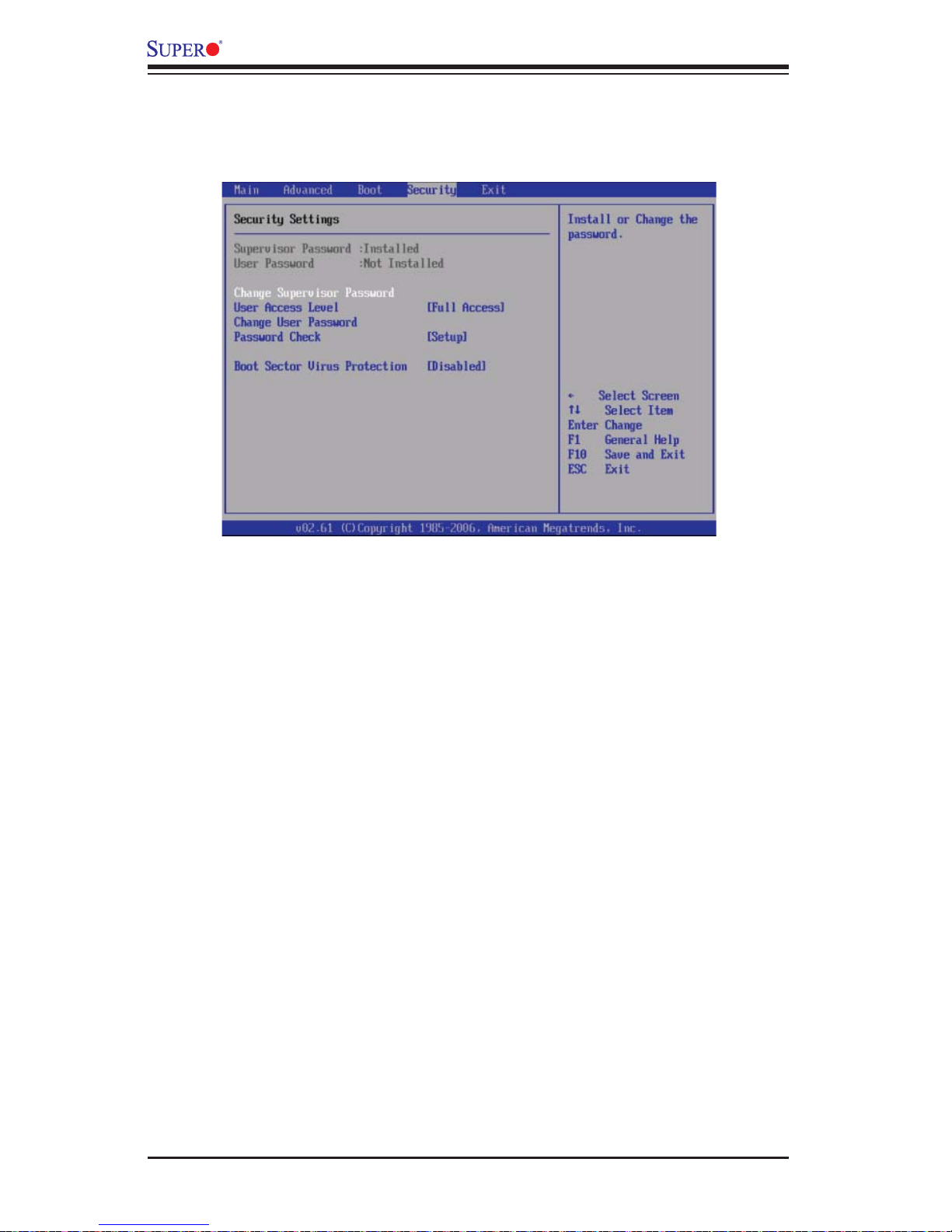
X8QB6-F/X8QBE-F Motherboard User’s Manual
5-5 Security Settings
The AMI BIOS provides a Supervisor and a User password. If you use both passwords, the Supervisor password must be set fi rst.
Supervisor Password
This item indicates if a Supervisor password has been entered for the system. "Not
Installed" means a Supervisor password has not been used.
User Password
This item indicates if a user password has been entered for the system. "Not I nstalle d" means that a u ser password has not been used.
Change Supervisor Password
Select this feature and press <Enter> to access the submenu, and then enter a
new Supervisor Password.
User Access Level (Available when Supervisor Password is set as above)
Select Full Access to grant full User read and write access to the Setup Utility.
Select View Only to allow the user to view the Setup Utility settings without changing the fi elds. Select Limited to allow the user to access and change limited fi elds
such as Date and Time. Select No Access to prevent the user from accessing the
Setup Utility.
Change User Password
Select this feature and press <Enter> to access the submenu and enter a new
User Password.
Clear User Password (Available only when User Password has been set)
This item allows the user to clear a user password after it has been entered.
5-30
 Loading...