

Page 1

X8DTT
X8DTT-F
X8DTT-IBX
X8DTT-IBXF
X8DTT-IBQ
X8DTT-IBQF
USER’S MANUAL
Revision 1.0b
Page 2

The information in this User’s Manual has been carefully reviewed and is believed to be accurate.
The vendor assumes no responsibility for any inaccuracies that may be contained in this document,
makes no commitment to update or to keep current the information in this manual, or to notify any
person or organization of the updates. Please Note: For the most up-to-date version of this
manual, please see our web site at www.supermicro.com.
Super Micro Computer, Inc. ("Supermicro") reserves the right to make changes to the product
described in this manual at any time and without notice. This product, including software and documentation, is the property of Supermicro and/or its licensors, and is supplied only under a license.
Any use or reproduction of this product is not allowed, except as expressly permitted by the terms
of said license.
IN NO EVENT WILL SUPERMICRO BE LIABLE FOR DIRECT, INDIRECT, SPECIAL, INCIDENTAL,
SPECULATIVE OR CONSEQUENTIAL DAMAGES ARISING FROM THE USE OR INABILITY TO
USE THIS PRODUCT OR DOCUMENTATION, EVEN IF ADVISED OF THE POSSIBILITY OF
SUCH DAMAGES. IN PARTICULAR, SUPERMICRO SHALL NOT HAVE LIABILITY FOR ANY
HARDWARE, SOFTW ARE, OR DA TA STORED OR USED WITH THE PRODUCT, INCLUDING THE
COSTS OF REPAIRING, REPLACING, INTEGRATING, INSTALLING OR RECOVERING SUCH
HARDWARE, SOFTWARE, OR DATA.
Any disputes arising between manufacturer and customer shall be governed by the laws of Santa
Clara County in the State of California, USA. The State of California, County of Santa Clara shall
be the exclusive venue for the resolution of any such disputes. Super Micro's total liability for all
claims will not exceed the price paid for the hardware product.
FCC Statement: This equipment has been tested and found to comply with the limits for a Class
A digital device pursuant to Part 15 of the FCC Rules. These limits are designed to provide
reasonable protection against harmful interference when the equipment is operated in a commercial
environment. This equipment generates, uses, and can radiate radio frequency energy and, if not
installed and used in accordance with the manufacturer’s instruction manual, may cause harmful
interference with radio communications. Operation of this equipment in a residential area is likely
to cause harmful interference, in which case you will be required to correct the interference at your
own expense.
California Best Management Practices Regulations for Perchlorate Materials: This Perchlorate
warning applies only to products containing CR (Manganese Dioxide) Lithium coin cells. “Perchlorate
Material-special handling may apply. See www.dtsc.ca.gov/hazardouswaste/perchlorate”
WARNING: Handling of lead solder materials used in this
product may expose you to lead, a chemical known to
the State of California to cause birth defects and other
reproductive harm.
Manual Revision 1.0b
Release Date: June 18, 2013
Unless you request and receive written permission from Super Micro Computer, Inc., you may not
copy any part of this document.
Information in this document is subject to change without notice. Other products and companies
referred to herein are trademarks or registered trademarks of their respective companies or mark
holders.
Copyright © 2013 by Super Micro Computer, Inc.
All rights reserved.
Printed in the United States of America
Page 3

Preface
About This Manual
This manual is written for system integrators, PC technicians and knowledgeable
PC users. It provides information for the installation and use of the X8DTT/
X8DTT-F/X8DTT-IBX/X8DTT-IBXF/X8DTT-IBQ/X8DTT-IBQF motherboard.
About This Motherboard
The X8DTT Series motherboards support the Intel 5500/5600 Series
Processor platform and the QuickPath Interconnect (QPI) Technology , providing the
next generation point-to-point system interface, replacing the current Front Side Bus.
With the 5500/5600 Series Processor built-in, the X8DTT/-F/-IBX/-IBXF/-IBQ/-IBQF
offers substantial enhancement in system performance with increased bandwidth
and unprecedented scalability optimized for HPC/Cluster, high-end servers and
intensive applications. Please refer to our web site (http://www.supermicro.com/
products/) for updates on supported processors. This product is intended to be
installed and serviced by professional technicians.
Preface
Manual Organization
Chapter 1 describes the features, specifi cations and performance of the mother-
board and provides detailed information about the chipset.
Chapter 2 provides hardware installation instructions. Read this chapter when in-
stalling the processor, memory modules and other hardware components into the
system. If you encounter any problems, see Chapter 3, which describes troubleshooting procedures for video, memory and system setup stored in the CMOS.
Chapter 4 includes an introduction to BIOS and provides detailed information on
running the CMOS Setup utility.
Appendix A lists BIOS POST Error Codes. Appendix B provides Software Installation Instructions.
iii
Page 4

X8DTT/-F/-IBX/-IBXF/-IBQ/-IBQF User's Manual
Conventions Used in the Manual
Special attention should be given to the following symbols for proper installation
and to prevent product damage or bodily injury:
Warning: Important information given to ensure proper system installation or to prevent
damage to the components.
Note: Additional Information given to differentiate various models or to
ensure correct system setup.
iv
Page 5

Contacting Supermicro
Headquarters
Address: Super Micro Computer, Inc.
980 Rock Ave.
San Jose, CA 95131 U.S.A.
Tel: +1 (408) 503-8000
Fax: +1 (408) 503-8008
Email: marketing@supermicro.com (General Information)
support@supermicro.com (Technical Support)
Contacting Supermicro
Web Site:
Europe
Address: Super Micro Computer B.V.
Tel: +31 (0) 73-6400390
Fax: +31 (0) 73-6416525
Email: sales@supermicro.nl (General Information)
Asia-Pacifi c
Address: Super Micro Computer, Inc.
www.supermicro.com
Het Sterrenbeeld 28, 5215 ML
's-Hertogenbosch, The Netherlands
support@supermicro.nl (Technical Support)
rma@supermicro.nl (Customer Support)
3F, No. 150, Jian 1st Rd.
Zhonghe Dist., New Taipei City 23511
Taiwan (R.O.C)
Tel: +886-(2) 8226-3990
Fax: +886-(2) 8226-3992
Web Site:
Technical Support:
Email: support@supermicro.com.tw
Tel: +886-(2)-8226-3990
www.supermicro.com.tw
v
Page 6

X8DTT/-F/-IBX/-IBXF/-IBQ/-IBQF User's Manual
Table of Contents
Table of Contents
Preface
Chapter 1 Introduction
1-1 Overview ........................................................................................................1-1
1-2 Chipset Overview ............................................................................................1-9
1-3 Special Features ...........................................................................................1-10
1-4 PC Health Monitoring .................................................................................... 1-10
1-5 ACPI Features ................................................................................................1-11
1-6 Power Supply ................................................................................................1-12
1-7 Overview of the Nuvoton WPCM450 Controller ........................................... 1-12
Chapter 2 Installation
2-1 Standardized Warning Statements ................................................................. 2-1
2-2 Static-Sensitive Devices ..................................................................................2-4
2-3 Motherboard Installation ..................................................................................2-5
Tools Needed .................................................................................................. 2-5
Installation Instructions ....................................................................................2-5
2-4 Processor and Heatsink Installation................................................................2-6
Installing a CPU Heatsink ............................................................................... 2-8
2-5 Memory Installation ...................................................................................... 2-10
2-6 Control Panel Connectors/IO Ports...............................................................2-15
Back Panel Connectors/IO Ports .................................................................. 2-15
Back Panel Connector Pin Defi nitions .......................................................... 2-16
Universal Serial Bus (USB) ...................................................................... 2-16
Ethernet Ports .......................................................................................... 2-17
Serial Ports ............................................................................................... 2-18
Video Connector .......................................................................................2-18
Infi niBand Connection (X8DTT-IBX/IBXF/IBQ/IBQ/IBQF) ........................2-19
Unit Identifi er Switches .............................................................................2-20
Front Control Panel ....................................................................................... 2-21
Front Control Panel Pin Defi nitions............................................................... 2-22
Power LED ..............................................................................................2-22
HDD/FP UID Switch ................................................................................. 2-22
NIC1 LED Indicator .................................................................................. 2-23
NIC2 LED Indicator .................................................................................. 2-23
Overheat (OH)/Fan Fail/PWR Fail/UID LED ............................................2-24
Power Fail LED ........................................................................................ 2-24
Reset Button ........................................................................................... 2-25
vi
Page 7

Table of Contents
Power Button ...........................................................................................2-25
2-7 Connecting Cables ........................................................................................ 2-26
20-pin Proprietary Power Connectors ...................................................... 2-26
4-pin Auxiliary Power Connector .............................................................2-27
Fan Headers ............................................................................................. 2-28
NMI Header ..............................................................................................2-29
Internal Buzzer ......................................................................................... 2-29
Wake-On-LAN ..........................................................................................2-30
T-SGPIO Headers .................................................................................... 2-30
SMB (I
IPMB I
2
C) Connector ................................................................................ 2-31
2
C SMB (For X8DTT-F/IBXF/IBQF only) ....................................... 2-31
2-8 Jumper Settings ............................................................................................ 2-32
Explanation of Jumpers ................................................................................ 2-32
GLAN Enable/Disable .............................................................................. 2-32
CMOS Clear .............................................................................................2-33
Watch Dog Enable/Disable ...................................................................... 2-33
Power Setting Select ................................................................................ 2-34
VGA Enable .............................................................................................. 2-34
J_UID_OW (-Overwriting) ........................................................................2-35
BMC Enable (For X8DTT-F/IBXF/IBQF only) .......................................... 2-36
2-9 Onboard Indicators ........................................................................................ 2-37
GLAN LEDs .............................................................................................. 2-37
BMC Heartbeat LED (X8DTT-F/IBX-F/IBQF) ........................................... 2-37
Infi niBand LED Indicators (LEB1/LEB2) (X8DTT-IBX/IBXF/IBQ/IBQF) ...2-38
Onboard Power LED
.....................................................................2-38
2-10 Serial ATA and PCI-E Connections ............................................................... 2-39
Serial ATA Ports........................................................................................ 2-39
PCI-Express x16 Gen. 2 Slot ................................................................... 2-39
Chapter 3 Troubleshooting
3-1 Troubleshooting Procedures ........................................................................... 3-1
3-2 Technical Support Procedures ........................................................................ 3-3
3-3 Frequently Asked Questions ........................................................................... 3-3
3-4 Returning Merchandise for Service.................................................................3-4
Chapter 4 BIOS
4-1 Introduction ...................................................................................................... 4-1
4-2 Main Setup ......................................................................................................4-2
4-3 Advanced Setup Confi gurations...................................................................... 4-4
4-4 Security Settings ........................................................................................... 4-25
vii
Page 8

X8DTT/-F/-IBX/-IBXF/-IBQ/-IBQF User's Manual
4-5 Boot Confi guration ........................................................................................4-26
4-6 Exit Options ................................................................................................... 4-27
Appendix A BIOS Error Beep Codes
A-1 BIOS Error Beep Codes ................................................................................. A-1
Appendix B Software Installation Instructions
B-1 Installing Software Programs .......................................................................... B-1
B-2 Confi guring Super Doctor® III ......................................................................... B-2
viii
Page 9

Chapter 1: Introduction
Chapter 1
Introduction
1-1 Overview
Checklist
Congratulations on purchasing your computer motherboard from an acknowledged
leader in the industry. Supermicro boards are designed with the utmost attention to
detail to provide you with the highest standards in quality and performance. Check
that the following items have all been included with your motherboard. If anything
listed here is damaged or missing, contact your retailer.
The following items are included in the bulk package.
• One (1) Supermicro Mainboard
• Two (2) Serial ATA cables (CBL-0044Lx2)
Note: For your system to work properly, please follow the links below to
download all necessary drivers/utilities and the user's manual for your
motherboard.
SMCI product mauals: http://www.supermicro.com/support/manuals/
Product Drivers and utilities: ftp://ftp.supermicro.com/
If you have any questions, please contact our support team at support@supermicro.
com.
1-1
Page 10
X8DTT/-F/-IBX/-IBXF/-IBQ/-IBQF User's Manual
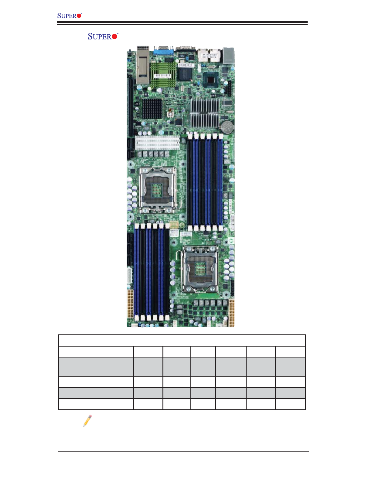
X8DTT/-F/-IBX/-IBXF/-IBQ/-IBQF Motherboard Image
Model Variations (Differences between X8DTT models)
IPMI 2.0 w/ KVM Over
LAN
Infi niBand Connect. No No Yes Yes Yes Yes
DDR IB No No Yes Yes No No
QDR IB No No No No Yes Yes
Note: The drawings and pictures shown in this manual were based on the
latest PCB Revision available at the time of publishing of the manual. The
motherboard you’ve received may or may not look exactly the same as
the graphics shown in the manual.
X8DTT /-F /-IBX /-IBXF /-IBQ /IBQF
No Yes No Yes No Yes
1-2
Page 11
Chapter 1: Introduction
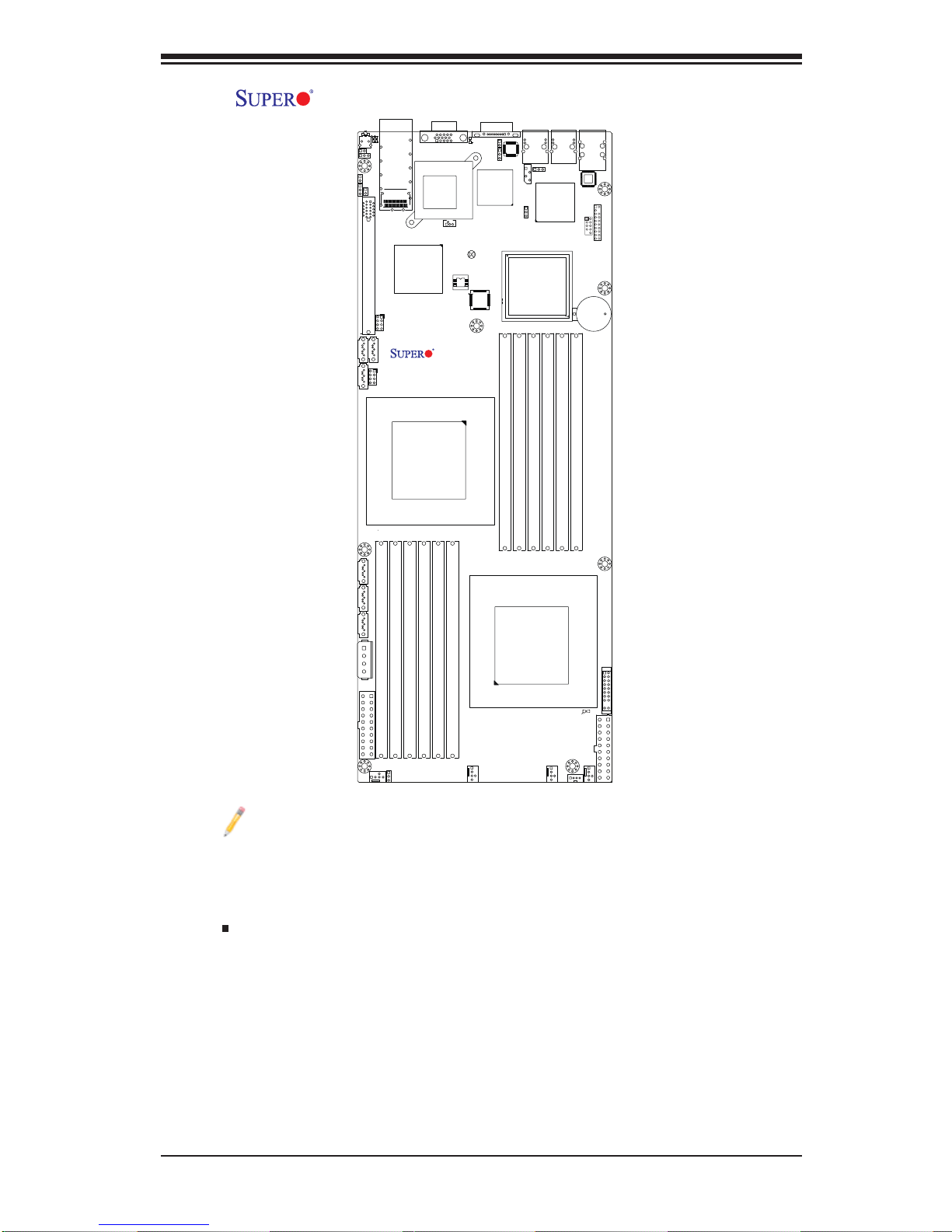
X8DTT/-F/-IBX/-IBXF/-IBQ/-IBQF Motherboard Layout
LE4
SW1
JNMI1
JWD1
JSPK1
J_UID_OW
J119
PCI-E 2.0 GEN2 X16
I-SATA0
I-SATA2
J19
I-SATA1
Intel
ICH-10R
(South Bridge)
CPU2
InfiniBand CTRL
VGA
X8DTT Series
Rev. 2.0
LEB2
LEB1
InfiniBand
Connector
T-SGPIO0
T-SGPIO1
COM1
LE2
JBMC1JPB
LAN2
IPMB
P2 DIMM1B
JPL1
(North Bridge)
P2 DIMM1A
Intel
5520/5500
P2 DIMM2B
JPG1
Nuvoton
WPCM450
JWOL1
JBT1
BIOS
LAN CTRL
P2 DIMM2A
LAN1
P2DIMM3B
P2DIMM3A
USB0/1
IPMI_LAN
PHY
JTPM1
USB2/3
JBAT1
Battery
I-SATA3
I-SATA4
I-SATA5
JP10
4-pin PWR
P1 DIMM3A
P1 DIMM2A
P1 DIMM2B
P1 DIMM1A
P1 DIMM1B
FAN3
P1 DIMM3B
JWR2
FAN4
JPEN1
CPU1
JF1
LE1
JWR1
FAN1
PWR I2C
FAN2
J18
Notes:
1. Jumpers not indicated are for test purposes only. For more information on
jumpers or components, refer to Chapter 2.
2. " " indicates the location of Pin 1.
3. When LEa LED is on, the onboard power connection is on. Make sure to
unplug the power cables before removing or installing components.
4. To use Hot-swap support on the 827 chassis, connect a cable to pins 2~3 on
JPEN1. Close pins 1~2 of JPEN1 with a cap to use regular PWR setting.
Warning: To avoid possible system overheating, please be sure to provide adequate
airfl ow to your system.
1-3
Page 12
X8DTT/-F/-IBX/-IBXF/-IBQ/-IBQF User's Manual
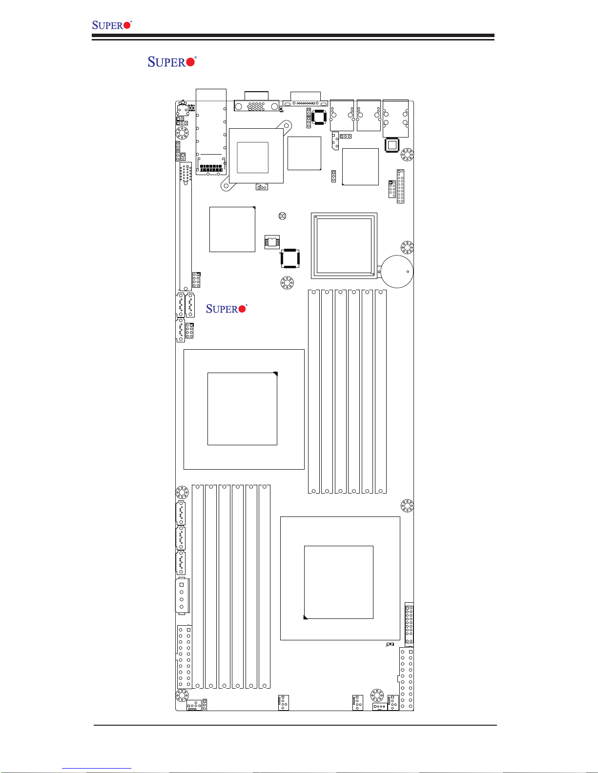
X8DTT/-F/-IBX/-IBXF/-IBQ/-IBQF Quick Reference
LE4
LEB1
SW1
JNMI1
JWD1
JSPK1
J_UID_OW
J119
PCI-E 2.0 GEN2 X16
I-SATA0
I-SATA2
J19
I-SATA1
VGA
LEB2
InfiniBand
Connector
InfiniBand CTRL
JWOL1
Intel
ICH-10R
(South Bridge)
T-SGP IO0
BIOS
COM1
LE2
JBMC1JPB
Nuvoton
WPCM450
JBT1
IPMB
JPL1
5520/5500
(North Bridge)
LAN2
JPG1
LAN CTRL
Intel
USB0/1
LAN1
IPMI_LAN
PHY
JTPM1
USB2/3
JBAT1
Battery
X8DTT Series
T-SGP IO1
Rev. 2.0
P2 DIMM1A
CPU2
I-SATA3
I-SATA4
I-SATA5
JP10
4-pin PWR
P1 DIMM3A
JWR2
P1 DIMM3B
P1 DIMM2A
P1 DIMM2B
P1 DIMM1A
P1 DIMM1B
P2 DIMM1B
CPU1
P2 DIMM2B
P2DIMM3B
JF1
LE1
JWR1
P2DIMM3A
P2 DIMM2A
FAN4
JPEN1
FAN3
FAN2
J18
FAN1
PWR I2C
1-4
Page 13

Chapter 1: Introduction
Quick Reference (See Chapter 2 for Details)
Jumper Description Default Setting
JBMC1 BMC Enable (X8DTT-F/-IBXF/-IBQF) Pins 1-2 (Enabled)
JBT1 CMOS Clear (See Section 2-8)
JPEN1 Normal Power Enable (Note 1-4 on P. 1-3) Pins 1-2 (Enabled)
JPG1 VGA Enable Pins 1-2 (Enabled)
JPL1 LAN1/2 Enable Pins 1-2 (Enabled)
J_UID_OW Red LED OW (Pins 7/8 of JF1) (Page 2-31) Off (Overwrites)
JWD1 Watch Dog Pins 1-2 (Reset)
Connector Description
COM1 COM1 Serial Port
FAN 1-4 System/CPU Fan Headers
Infi niBand Infi niBand Connector (X8DTT-/IBX/IBXF/IBQ/IBQF)
IPMB IPMB Header (for an IPMI Card) (X8DTT-F/-IBXF/-IBQF)
J119 Infi niBand I
2
C Debug Header (-/IBX/IBXF/IBQ/IBQF)
JF1 Front Panel Connector
JNMI1 NMI (Non-Maskable Interrupt) Header
JP10 Onboard 4-pin Power Connector
JPSK1 Internal Speaker/Buzzer Header
JTPM1 Trusted Platform Module Header
JWR1/JWR2 12V 20-pin Power Connector (See P. 2-21)
JWOL1 Wake-On-LAN Header
LAN1/2 Gigabit Ethernet (RJ45) Ports
(IPMI dedicated) LAN LAN (RJ45) Port for IPMI 2.0 (X8DTT-F/-IBXF/-IBQF)
SATA0 ~ SATA5 (Intel South Bridge) SATA Ports
SMBus System Management Bus (SMBus) I
2
C Header (J18)
SW1 Unit Identifi er Switch
T-SGPIO-0/T-SGPIO-1 Serial General Purpose Input/Output Headers
USB0/1, USB 2/3 Universal Serial Bus (USB) Ports 0/1, 2/3
VGA Video Port
LED Description
LE1 On board S tandby P WR warn ing LED In dicato r
LE2 BMC Heartbeat LED (Green/Blinking: Normal) (X8DTT-F/-IBXF/-IBQF)
LE4 (Rear) Unit Identifi er (UID) LED Indicator
LEB1 Infi niBand Link LED (X8DTT-IBX/-IBXF/-IBQ/-IBQF)
LEB2 Infi niBand Activity LED (X8DTT-IBX/-IBXF/-IBQ/-IBQF)
1-5
Page 14

X8DTT/-F/-IBX/-IBXF/-IBQ/-IBQF User's Manual
Motherboard Features
CPU
• Two Intel
two full-width Intel QuickPath Interconnect (QPI) links with a total of up to 51.2
GT/s Data Transfer Rate (6.4 GT/s per direction)
Memory
®
5500/5600 Series (LGA 1366) processors, each processor supporting
• 12 240-pin DIMM sockets support up to 192 GB of Registered ECC or up to
48 GB of Unbuffered ECC/Non-ECC DDR3 1333/1066/800 MHz Memory (See
Section 2-4 in Chapter 2 for DIMM Slot Population.)
Chipset
• Intel 5520 chipset, including: the 5520 (North Bridge) and the ICH10R (South
Bridge).
Note: Intel 5500 Chipset is available for OEM only.
Expansion Slot
• One PCI-E x16 Gen. 2.0 slot
BIOS
• 32 Mb AMI SPI Flash ROM
• ACPI 1.0/2.0/3.0, Plug and Play (PnP), and USB Keyboard support
PC Health Monitoring
• Onboard voltage monitors for CPU1 VCore, CPU2 VCore, +5Vin, 12Vcc (V),
VP1 DIMM, VP2 DIMM, +3.3Vcc (V), and Battery Voltage
• Fan status monitor with fi rmware control
• CPU/chas sis tempe rature mo nitors
• Plat form Envir onment C ontro l Inter face ( PECI) ready
• CPU fan a uto -of f in sl eep mo de
• CPU slo w-d own on tem peratur e overheat
• Pulse W idth M odulat ion (PW M) Fan Cont rol
• CPU th ermal t rip su ppor t for p roce ssor p rotect ion, powe r LED
• Power-up mo de co ntrol fo r rec overy f rom AC powe r loss
• Auto -sw itchin g voltag e regul ator for C PU cor es
• System ove rheat / Fan Fail LED Indic ator an d cont rol
• System r esour ce ale rt v ia Supe ro Doc tor II I
ACPI Features
• Slow blinking LED for suspend state indicator
• Main switch override mechanism
1-6
Page 15

Chapter 1: Introduction
• ACPI Po wer M ana gem ent
• Keyboard Wakeup from Soft-off
Onboard I/O
• Intel ICH10R supports six SATA ports (RAID0, RAID1, RAID10, RAID5 supported
in the Windows OS Environment and RAID 0, RAID 1, RAID 10 supported for
the Linux OS)
• Nuvoton W P CM 45 0 B M C (Ba seb oa rd M ana gem ent C ont ro lle r) supp orts IP MI
2.0 with K V M supp or t (X8DTT-F/-IBXF/-IBQF)
• Intel 82576 D ual - L A N Gi gabi t Ether net C ont roll er sup ports du al Gi ga -b it L A N
ports
• Onbo ard PHY Ch ip suppo rt s IPMI de dicate d LA N (X8 DTT-F/-IBX F/-IBQ F)
• One C OM por t
• Infi niBand Connector
• Up to fou r USB 2.0 (Univer sal Seria l Bus) conne ctions (2 Por ts and 2 Front
Headers)
• Super I /O: Winb ond W8 3527HG
Other
• Wake-on-LAN (WOL)
• Console redirection
• Onbo ard Fan Spe ed Cont rol by The rmal M anage ment via B IOS
CD/Diskette Utilities
• BIOS fl ash upgrade utility and device drivers
Dimensions
• Propr ieta ry 16.6 4" (L) x 6.5 0" ( W) (422.6 6 mm x 165.10 mm)
1-7
Page 16

X8DTT/-F/-IBX/-IBXF/-IBQ/-IBQF User's Manual
QSFP
#1
#1
#1
DDR3 DIMM
#2
#2
#2
AA
BB
CC
DDR3 DIMM
MT25408
Connect-X IB
PCI-E Gen2/DDR or QDR
(Depupulate
for 5500)
DDR II
PROCESSOR#0
Port1 Port0
Ports
3,4
Ports
5,6
Ports
7,8,9,10
PCI-E x16 Slot
PE
5
4-1
PE
WBD
BMC/VGA
Intel 5520/5500
PCI
PROCESSOR#1
Ports
2,1
CLINK
ESI
CLINK
DMI
ICH10R
LPC
F
Kawela
RJ45 RJ45
SST25
VF016
SPI
SATA
SATA #1
SATA #2
SATA #3
SATA #4
SATA #5
SATA #6
LPCIO W83527
ACPI
KBC
#2
#2
#2
DDR3 DIMM
#1
#1
#1
DD
EE
F
DDR3 DIMM
VGA CONN
RTL8201N PHY
Dedicate LAN
Block Diagram of the 5500/5600 Series Processor Platform
Note 1: This is a general block diagram. Please see the previous Mother-
board Features pages for details on the features of each motherboard.
Note 2: Intel 5500 Chipset is available for OEM only.
1-8
Page 17

Chapter 1: Introduction
1-2 Chipset Overview
Built up on th e fun cti ona lit y an d the c ap abil it y of th e 55 0 0/5 6 0 0 Ser ie s Pro ce sso r
platf orm, t he X8DT T/-F/-IBX /- IBXF/- IBQ /- IBQF m other board p rovide s the per fo rmance a nd feature set req uired for dual -proc essor-bas ed systems wit h confi gu-
ration o ption s optimi zed for inte nsive app licat ions, H igh Per fo rman ce Co mputi ng
(HPC)/Cluster and server platforms. The 550 0/5600 Series Processor platform
consists of the 550 0/ 5 600 Series (LGA 1366) processor, the 5520 (North Bridge),
and the IC H10R (South Br id ge). With th e Intel Q uic kPat h inter co nne ct (QPI) c on troller built-in, the 5500/5600 Series Processor platform is the fi rst dual-proce ssi n g
platform to offer the next generation point-to-point system interconnect interface
that replaces the current Front Side Bus Technology, substantially enhancing
system performance by utilizing serial link interconnections, allowing for increased
bandwidth and scalability.
The IOH connects to each processor through an independent QPI (QuickPath
interconnect) link. Each link consists of 20 pairs of unidirectional differential lanes
for tra nsmis sio n and re cei ving i n addit ion t o a dif fer entia l for wa rded c lo ck. A f ull width Q PI link pair p rovide s 84 si gnals. Ea ch proc ess or suppo rt s two Q uickPat h
links, one g oing to th e other pr oce ssor an d the othe r to the 5 520.
The 552 0 suppor ts up to 36/ 24 PCI Expre ss Gen2 lan es peer-to -peer rea d and
write transactions. The ICH10R provides multiple PCI-Express SATA and USB
connections.
In additi on, th e 55 00 /5 60 0 Se rie s Proc es sor pl atf or m also of fe rs a w ide ra nge of
RA S (Reliabilit y, Availabili ty and Ser vice ability) featur es. These feat ures inclu de
memor y i nter fa ce ECC, x4 /x8 S ing le Devi ce D ata C or rec tio n (SDD C), Cyclic Re dundancy Check (CRC), parity protection, out-of-band register access via SMBus,
memory mirroring, memory sparing, and Hot-plug support on the PCI-Express
Interface.
Note: Intel 5500 Chipset is available for OEM only.
Main Features of the 5500/5600 Series Processor and the
5520 Chipset
• Four processor cores in each processor with 8MB shared cache among cores
• Two full-width Intel QuickPath interconnect links, up to 6.4 GT/s of data transfer
rate in each direction
• Virtualization Technology, Integrated Management Engine supported
• Point-to-point cache coherent interconnect, Fast/narrow unidirectional links, and
Concurrent bi-directional traffi c
1-9
Page 18

X8DTT/-F/-IBX/-IBXF/-IBQ/-IBQF User's Manual
1-3 Special Features
Recovery from AC Power Loss
BIOS provides a setting for you to determine how the system will respond when AC
power is lost and then restored to the system. You can choose for the system to
remain powered off (in which case you must press the power switch to turn it back
on) or for it to automatically return to a power- on state. See the Advanced BIOS
Setup section to change this setting. The default setting is Last State.
1-4 PC Health Monitoring
This section describes the PC health monitoring features of the X8DTT/-F/-IBX/IBXF/-IBQ/-IBQF. All have an onboard System Hardware Monitor chip that supports PC health monitoring. An onboard voltage monitor will scan these onboard
voltages continuously: CPU1 VCore, CPU2 VCore, +5Vin, 12Vcc (V), VP1 DIMM,
VP2 DIMM, +3.3Vcc (V), and Battery Voltage. Once a voltage becomes unstable,
a warning is given or an error message is sent to the screen. Users can adjust the
voltage thresholds to defi ne the sensitivity of the voltage monitor.
Fan Status Monitor with Firmware Control
The PC health monitor can check the RPM status of the cooling fans. The onboard
CPU and chassis fans are controlled by Thermal Management via BIOS (under
Hardware Monitoring in the Advanced Setting).
Environmental Temperature Control
The thermal control sensor monitors the CPU temperature in real time and will turn
on the thermal control fan whenever the CPU temperature exceeds a user-defi ned
threshold. The overheat circuitry runs independently from the CPU. Once it detects
that the CPU temperature is too high, it will automatically turn on the thermal fan
control to prevent any overheat damage to the CPU. The onboard chassis thermal
circuitry can monitor the overall system temperature and alert users when the chassis temperature is too high.
Warning: To avoid possible system overheating, please be sure to provide
adequate airfl ow to your system.
System Resource Alert
This feat ure is available wh en used with Sup er Doctor ® III in the Win dows OS
environment or used with Super Doctor II in Linux. Super Doctor is used to
notif y the user of cer tain system events. For example, you can also confi gure
1-10
Page 19

Chapter 1: Introduction
Super Do ctor to provi de you with warn ings when the sys tem temperatur e, CPU
temperat ures, volt ages a nd fan spe eds go beyon d a pre- defi ned range.
1-5 ACPI Features
ACPI stands for Advanced Confi guration and Power Interface. The ACPI specifi ca-
tion defi nes a fl exible and abstract hardware interface that provides a standard
way to integrate power management features throughout a PC system, including
its hardware, operating system and application software. This enables the system
to automatically turn on and off peripherals such as CD-ROMs, network cards, hard
disk drives and printers.
In addition to enabling operating system-directed power management, ACPI
provides a generic system event mechanism for Plug and Play and an operating
system-independent interface for confi guration control. ACPI leverages the Plug
and Play BIOS data structures while providing a processor architecture-independent
implementation that is compatible with Windows XP/Windows 2003/Windows 2008/
Windows Vista Operating Systems.
Slow Blinking LED for Suspend-State Indicator
When the CPU goes into a suspend state, the chassis power LED will start blinking
to indicate that the CPU is in suspend mode. When the user presses any key, the
CPU will wake-up and the LED will automatically stop blinking and remain on.
Main Switch Override Mechanism
When an ATX power supply is used, the power button can function as a system
suspend button to make the system enter a SoftOff state. The monitor will be
suspended and the hard drive will spin down. Pressing the power button again
will cause the whole system to wake-up. During the SoftOff state, the ATX power
supply provides power to keep the required circuitry in the system "alive." In case
the system malfunctions and you want to turn off the power, just press and hold
the power button for 4 seconds. This option can be set in the Power section of the
BIOS Setup routine.
Wake-On-LAN (WOL)
Wake-On-LAN is defi ned as the ability of a management application to remotely
power up a computer that is powered off. Remote PC setup, up-dates and asset
tracking can occur after hours and on weekends so that daily LAN traffi c is kept
to a minimum and users are not interrupted. The motherboard has a 3-pin header
(WOL) to connect to the 3-pin header on a Network Interface Card (NIC) that has
WOL capability. In addition, an onboard LAN controller can also support WOL
1-11
Page 20

X8DTT/-F/-IBX/-IBXF/-IBQ/-IBQF User's Manual
without any connection to the WOL header. The 3-pin WOL header is to be used
with a LAN add-on card only.
Note: Wake-On-LAN requires an ATX 2.01 (or above) compliant power
supply.
1-6 Power Supply
As with all computer products, a stable power source is necessary for proper and
reliable operation. It is even more important for processors that have high CPU
clock rates.
It is strongly recommended that you use a high quality power supply that meets ATX
power supply Specifi cation 2.02 or above. It must also be SSI compliant (For more
information, please refer to the web site at http://www.ssiforum.org/). Additionally, in
areas where noisy power transmission is present, you may choose to install a line
fi lter to shield the computer from noise. It is recommended that you also install a
power surge protector to help avoid problems caused by power surges.
Note: The X8DTT/-F/-IBX/-IBXF/-IBQ/-IBQF supports proprietary power
connectors. Please refer to Page 2-21 for detailed information on power
supply for the motherboard.
1-7 Overview of the Nuvoton WPCM450 Controller
The Nuvoton WPCM450, a Baseboard Management Controller (BMC), supports
the 2D/VGA-compatible Graphics Core with the PCI interface, Virtual Media, and
Keyboard/Video/Mouse (KVM) Redirection modules.
The WPCM450 BMC interfaces with the host system via a PCI interface to communicate with the graphics core. It supports USB 2.0 and 1.1 for remote keyboard/
mouse/virtual media emulation. It also provides LPC interface to control Super IO
functions. The WPCM450 is connected to the network via an external Ethernet
PHY module.
The WPCM450 communicates with onboard components via six SMBus interfaces,
fan control, Platform Environment Control Interface (PECI) buses.
Note: For more information on IPMI confi guration, please refer to the
Embedded IPMI User's Guide posted on our website @ http://www.supermicro.com/support/manuals/.
1-12
Page 21

Chapter 2: Installation
Chapter 2
Installation
2-1 Standardized Warning Statements
The following statements are industry-standard warnings, provided to warn the user
of situations which have the potential for bodily injury . Should you have questions or
experience diffi culty, contact Supermicro's Technical Support department for assis-
tance. Only certifi ed technicians should attempt to install or confi gure components.
Read this section in its entirety before installing or confi guring components in the
Supermicro chassis.
Battery Handling
Warning!
There is a danger of explosion if the battery is replaced incorrectly. Replace the
battery only with the same or equivalent type recommended by the manufacturer.
Dispose of used batteries according to the manufacturer's instructions
電池の取り扱い
電池交換が正しく行われなかった場合、破裂の危険性があります。交換する電池はメー
カーが推奨する型、または同 等のものを使 用下さい。使用済電池は製造元の指示に従
って処 分して 下さい 。
警告
电池更换不当会有爆炸危险。请只使用同类电池或制造商推荐的功能相当的电池更
换原有电池。请按制造商的说明处理废旧电池。
警告
電池更換不當會有爆炸危險。請使用製造商建議之相同或功能相當的電池更換原有
電池。請按照製造商的說明指示處理廢棄舊電池。
Warnung
Bei Einsetzen einer falschen Batterie besteht Explosionsgefahr. Ersetzen Sie die
Batterie nur durch den gleichen oder vom Hersteller empfohlenen Batterietyp.
Entsorgen Sie die benutzten Batterien nach den Anweisungen des Herstellers.
2-1
Page 22

X8DTT/-F/-IBX/-IBXF/-IBQ/-IBQF User's Manual
!הרהזא
Attention
ﻲﺋﺎﻬﻨﻟﺍ ﺺﻠﺨﺘﻟﺍ ﻦﻣ ﺞﺘﻨﻤﻟﺍ ﺍﺬﻫ ﻪﻌﻣ ﻞﻣﺎﻌﺘﻟﺍ ﻲﻐﺒﻨﻳ ﻟ ﺎﻘﻓﻭ ﻊﻴﻤﺠﺔﻴﻨﻁﻮﻟﺍ ﺢﺋﺍﻮﻠﻟﺍﻭ ﻦﻴﻧﺍﻮﻘﻟﺍ ﺪﻨﻋ
Danger d'explosion si la pile n'est pas remplacée correctement. Ne la remplacer
que par une pile de type semblable ou équivalent, recommandée par le fabricant.
Jeter les piles usagées conformément aux instructions du fabricant.
¡Advertencia!
Existe peligro de explosión si la batería se reemplaza de manera incorrecta. Re-
emplazar la batería exclusivamente con el mismo tipo o el equivalente recomendado por el fabricante. Desechar las baterías gastadas según las instrucciones
del fabricante.
תנכס תמייקץוציפ .הניקת אל ךרדב הפלחוהו הדימב הללוסה לש ףילחהל שי
גוסב הללוסה תא מ םאותה תרבחלמומ ןרציתצ.
תוללוסה קוליס תושמושמה עצבל שי .ןרציה תוארוה יפל
ﺮﻄﺧ ﻙﺎﻨﻫ ﻦﻣ ﻝﺍﺪﺒﺘﺳﺍ ﺔﻟﺎﺣ ﻲﻓ ﺭﺎﺠﻔﻧﺍ ﺔﻳﺭﺎﻄﺒﻟﺍ ﺔﺤﻴﺤﺻ ﺮﻴﻏ ﺔﻘﻳﺮﻄﺑ ﻚﻴﻠﻌﻓ
ﺔﻳﺭﺎﻄﺒﻟﺍ ﻝﺍﺪﺒﺘﺳﺍ
ﻂﻘﻓ ﻉﻮﻨﻟﺍ ﺲﻔﻨﺑ ﺎﻬﻟﺩﺎﻌﻳ ﺎﻣ ﻭﺃ ﺎﻤﻛﺖﺻﻭﺃ ﺔﻌﻨﺼﻤﻟﺍ ﺔﻛﺮﺸﻟﺍ ﻪﺑ
ﺕﺎﻳﺭﺎﻄﺒﻟﺍ ﻦﻣ ﺺﻠﺨﺗ ﻟ ﺎﻘﻓﻭ ﺔﻠﻤﻌﺘﺴﻤﻟﺍﺔﻌﻧﺎﺼﻟﺍ ﺔﻛﺮﺸﻟﺍ ﺕﺎﻤﻴﻠﻌﺘ
경고!
배터리가 올바르게 교체되지 않으면 폭발의 위험이 있습니다. 기존 배터리와 동일
하거나 제조사에서 권장하는 동등한 종류의 배터리로만 교체해야 합니다. 제조사
의 안내에 따라 사용된 배터리를 처리하여 주십시오.
Waarschuwing
Er is ontploffi ngsgevaar indien de batterij verkeerd vervangen wordt. Vervang de
batterij slechts met hetzelfde of een equivalent type die door de fabrikant aanbevolen wordt. Gebruikte batterijen dienen overeenkomstig fabrieksvoorschriften
afgevoerd te worden.
2-2
Page 23

Chapter 2: Installation
רצומה קוליס
Product Disposal
Warning!
Ultimate disposal of this product should be handled according to all national laws
and regulations.
製品の廃棄
この製品を廃棄処分する場合、国の関係する全ての法律・条例に従い処理する必要が
あります。
警告
本产品的废弃处理应根据所有国家的法律和规章进行。
警告
本產品的廢棄處理應根據所有國家的法律和規章進行。
Warnung
Die Entsorgung dieses Produkts sollte gemäß allen Bestimmungen und Gesetzen
des Landes erfolgen.
¡Advertencia!
Al deshacerse por completo de este producto debe seguir todas las leyes y regla-
mentos nacionales.
Attention
La mise au rebut ou le recyclage de ce produit sont généralement soumis à des
lois et/ou directives de respect de l'environnement. Renseignez-vous auprès de
l'organisme compétent.
!הרהזא
ו תויחנהל םאתהב תויהל בייח הז רצומ לש יפוס קוליס.הנידמה יקוח
ﻲﺋﺎﻬﻨﻟﺍ ﺺﻠﺨﺘﻟﺍ ﻦﻣ ﺞﺘﻨﻤﻟﺍ ﺍﺬﻫ ﻪﻌﻣ ﻞﻣﺎﻌﺘﻟﺍ ﻲﻐﺒﻨﻳ ﻟ ﺎﻘﻓﻭ ﻊﻴﻤﺠﺔﻴﻨﻁﻮﻟﺍ ﺢﺋﺍﻮﻠﻟﺍﻭ ﻦﻴﻧﺍﻮﻘﻟﺍ ﺪﻨﻋ
2-3
Page 24

X8DTT/-F/-IBX/-IBXF/-IBQ/-IBQF User's Manual
경고!
이 제품은 해당 국가의 관련 법규 및 규정에 따라 폐기되어야 합니다.
Waarschuwing
De uiteindelijke verwijdering van dit product dient te geschieden in overeenstemming
met alle nationale wetten en reglementen.
2-2 Static-Sensitive Devices
Electrostatic Discharge (ESD) can damage electronic com ponents. T o prevent damage to your system board, it is important to handle it very carefully. The following
measures are generally suffi cient to protect your equipment from ESD.
Precautions
• Use a grounded wrist strap designed to prevent static discharge.
• Touch a grounded metal object before removing the board from the antistatic
bag.
• Handle the board by its edges only; do not touch its components, peripheral
chips, memory modules or gold contacts.
• When handling chips or modules, avoid touching their pins.
• Put the motherboard and peripherals back into their antistatic bags when not
in use.
• For grounding purposes, make sure your computer chassis provides excellent
conductivity between the power supply, the case, the mounting fasteners and
the motherboard.
• Use only the correct type of onboard CMOS battery as specifi ed by the
manufacturer. Do not install the onboard battery upside down to avoid possible
explosion.
Unpacking
The motherboar d is shipped i n a ntistati c pa ckaging to avoid static da mage. When
unpacking the board, make sure the person handling it is static protected.
2-4
Page 25
Chapter 2: Installation
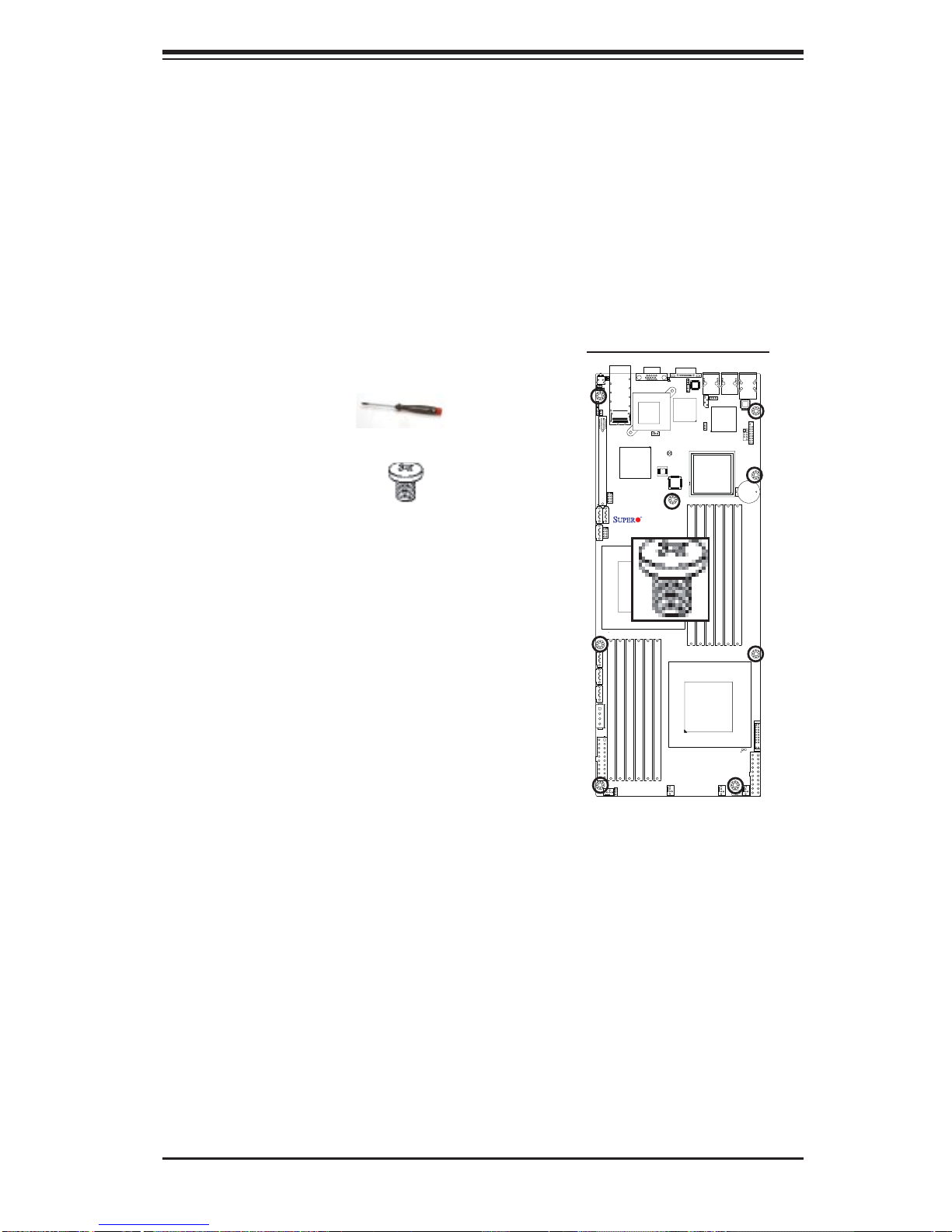
2-3 Motherboard Installation
All motherboards have standard mounting holes to fi t different types of chassis.
Make sure that the locations of all the mounting holes for both motherboard and
chassis match. Although a chassis may have both plastic and metal mounting
fasteners, metal ones are highly recommended because they ground the motherboard to the chassis. Make sure that the metal standoffs click in or are screwed in
tightly. Then use a screwdriver to secure the motherboard onto the motherboard
tray. Note: Some components are very close to the mounting holes. Please take
precautionary measures to prevent damage to these components when installing
the motherboard to the chassis.
Tools Needed
1. Phillips Screwdriver
2. Pan head #6 screws
Locations of Mounting Holes
X8DTT Series
Installation Instructions
Rev. 2.0
1. Install the IO shield into the chassis.
2. Locate the mounting holes on the motherboard. Refer to the layout above for mounting hole locations.
3. Locate the matching mounting holes on the
chassis. Align the mounting holes on the
motherboard against the mounting holes on
the chassis.
4. Install standoffs in the chassis as needed.
5. Install the motherboard into the chassis carefully to avoid damage to motherboard components.
Warning: To avoid damaging the motherboard and its components, please do not apply any force greater than 8 lb/sq.in (8 lbs. per square inch) when installing a screw
into a mounting hole.
6. Insert a Pan head #6 screw into a mounting hole on the motherboard and its
matching mounting hole on the chassis, using a Phillips screwdriver.
7. Repeat Step 4 to insert #6 screws to all mounting holes.
8. Make sure that the motherboard is securely placed on the chassis.
2-5
Page 26
X8DTT/-F/-IBX/-IBXF/-IBQ/-IBQF User's Manual
2-4 Processor and Heatsink Installation
Warning: When handling the processor package, avoid placing direct pressure on the
label area of the fan.
Notes:
1. Always connect the power cord last and always remove it before adding, removing or changing any hardware components. Make sure that you install the
processor into the CPU socket before you install the CPU heatsink.
2. Make sure to install the motherboard into the chassis before you install the
CPU heatsink and heatsink fans.
3. When purchasing a 5500/5600 Series processor or when receiving a motherboard with a 5500/5600 Series processor pre-installed, make sure that the
CPU plastic cap is in place, and none of the CPU pins are bent; otherwise,
contact the retailer immediately.
4. Refer to the M B Features S ecti on for mo re deta ils on CPU s uppor t.
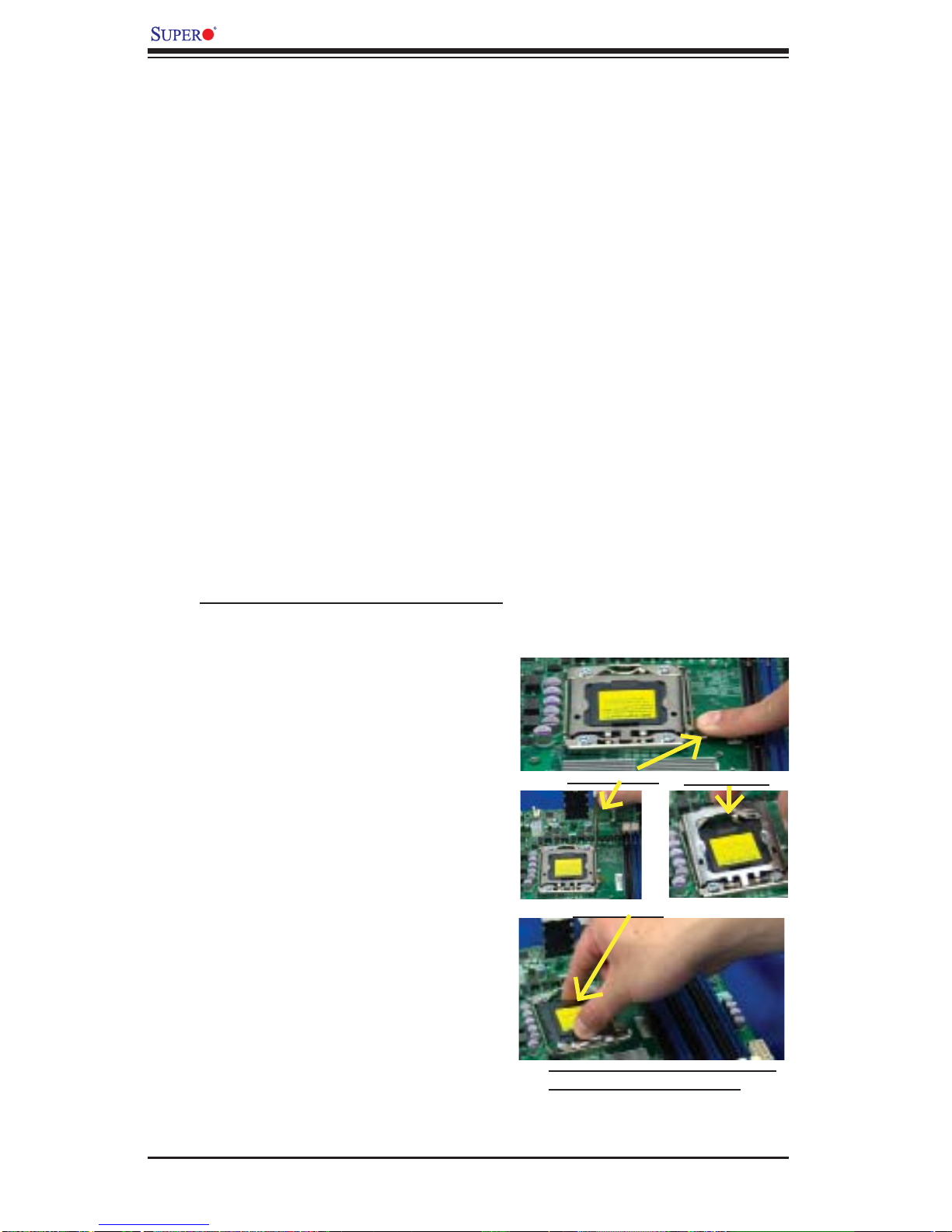
Installing an LGA 1366 Processor
1. Press the socket clip to release
the load plate, which covers the
CPU socket, from its locking
position.
Socket Clip
2. Gently lift the socket clip to
open the load plate.
Plastic Cap
3. Hold the plastic cap at its north
and south center edges to remove it from the CPU socket.
Load Plate
Hold the north & south edges of
the plastic cap to remove it
2-6
Page 27

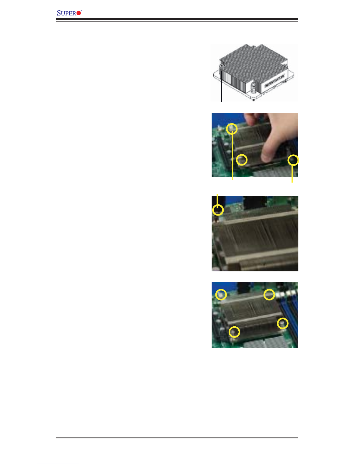
4. After removing the plastic cap, using
your thumb and the index fi nger,
hold the CPU at the north and south
center edges.
5. Align the CPU key, the semi-circle
cutout, against the socket key, the
notch below the gold color dot on
the side of the socket.
6. Once both the CPU and the socket
are aligned, carefully lower the CPU
straight down into the socket. (Do
not rub the CPU against the surface
of the socket or its pins to avoid
damaging the CPU or the socket.)
Chapter 2: Installation
Socket Keys CPU CPU SocketLoad Plate
7. With the CPU inside the socket, inspect the four corners of the CPU to
make sure that the CPU is properly
installed.
8. Once the CPU is securely seated
on the socket, lower the CPU load
plate to the socket.
9. Use your thumb to gently push the
socket clip down to the clip lock.
Warning: Please s ave th e p las ti c c a p. Th e
motherboard must be sh ipped with the pl astic cap properly installed to protect the CPU
socket pins. Shipment without the plastic
cap properly installed will cause damage
to the socket pins.
CPU Keys
2-7
Page 28
X8DTT/-F/-IBX/-IBXF/-IBQ/-IBQF User's Manual
Installing a CPU Heatsink
1. Do not apply any thermal
grease to the heatsink or the
CPU die because the required
amount has already been applied.
2. Place the heatsink on top of the
CPU so that the four mounting
holes are aligned with those on
the retention mechanism.
3. Install two diagonal screws (ie
the #1 and the #2 screws) and
tighten them until just snug (-do
not fully tighten the screws to
avoid possible damage to the
CPU.)
Screw#1
Screw#1
Install Screw#1
Screw#2
Screw#2
4. Finish the installation by fully
tightening all four screws.
2-8
Page 29
Chapter 2: Installation
Removing the Heatsink
Warning: We do not recommend that the CPU or the heatsink be removed. However,
if you do need to remove the heatsink, please follow the instructions below to uninstall
the heatsink and prevent damage to the CPU or other components.
1. Unplug the power cord from the
power supply.
2. Disconnect the heatsink fan
wires from the CPU fan header.
3. Using a screwdriver, loosen and
remove the heatsink screws
from the motherboard in the sequence as show in the picture
on the right.
Using a screwdriver to
remove Screw#1
4. Hold the heatsink as shown
in the picture on the right and
gently wriggle the heatsink to
loosen it from the CPU. (Do not
use excessive force when wriggling the heatsink.)
5. Once the heatsink is loosened,
remove it from the CPU socket.
6. To reinstall the CPU and the
heatsink, clean the surface of
the CPU and the heatsink to get
rid of the old thermal grease.
Reapply the proper amount of
thermal grease on the surface
before reinstalling them on the
motherboard.
Remove Screw#2
2-9
Page 30
X8DTT/-F/-IBX/-IBXF/-IBQ/-IBQF User's Manual
2-5 Memory Installation
Note: Check the S uper micro we b site for r ecom mende d memor y mo dules .
CAUTION
Exercise extreme care when installing or removing DIMM
module s to prevent any po ssib le damag e. Also n ote that th e
memor y is i nterl eaved to imp rove per fo rman ce (See ste p 1).
DIMM Installation
1. Insert the desired number of DIMMs into the memory slots, starting with
P1-DIMM 1A. For best memory performance, please install memory modules
of the same type and same speed on the memory slots as indicated on the
tables below. (See the Memory Installation Table Below.)
2. Insert each DIMM module vertically into its slot. Pay attention to the notch
along the bottom of the module to prevent inserting the DIMM module incorrectly.
3. Gently press down on the DIMM module until it snaps into place in the slot.
Repeat for all modules.
Memory Population for Optimal Performance
-For a motherboard with One CPU (CPU1) installed
Branch 0 Branch 1 Branch 2
3 DIMMs P1 DIMM1A P1 DIMM2A P1 DIMM3A
6 DIMMs P1 DIMM1A P1 DIMM1B P1 DIMM2A P1 DIMM2B P1 DIMM3A P1 DIMM3B
Memory Population for Optimal Performance
-For a motherboard with One CPU (CPU2) installed
Branch 0 Branch 1 Branch 2
3 DIMMs P2 DIMM1A P2 DIMM2A P2 DIMM3A
6 DIMMs P2 DIMM1A P2 DIMM1B P2 DIMM2A P2 DIMM2B P2 DIMM3A P2 DIMM3B
Memory Population for Optimal Performance
-For a motherboard with Two CPUs installed
CPU1 CPU2
Branch 0 Branch 1 Branch 3 Branch 0 Branch 1 Branch 3
6 DIMMs 1A 2A 3A 1A 2A 3A
12
DIMMs
1A 1B 2A 2B 3A 3B 1A 1B 2A 2B 3A 3B
2-10
Page 31

Chapter 2: Installation
Memory Support
This motherboard supports up to 192 GB of Registered ECC or 48 GB of Unbuffered
ECC/Non-ECC DDR3 1333/1066/800 MHz Memory in 12 DIMMs. Also, memory
speed support is dependent on the type of CPU used on the board.
DIMM Module Population Confi guration
For memor y to wor k pro perl y, follow the tab les be low for me mor y inst allati on:
Memory Support for the Motherboard w/5500 Processors Installed
RDIMM Population for the Motherboard with 5500 Processors Installed
DIMM
Slots per
Channel
2 1 Reg. DDR3 ECC 800,1066,1333 SR or DR
2 1 Reg. DDR3 ECC 800,1066 (Note 1) QR
2 2 Reg. DDR3 ECC 800,1066 (Note 1) Mixing SR, DR
2 2 Reg. DDR3 ECC 800 (Note 2) Mixing SR, DR, QR
Note 1: 1333 RDIMMs will run at 1066 MHz (-BIOS automatic downgrading).
Note 2: 1333/1066 RDIMMs will run at 800 MHz (-BIOS automatic downgrading).
DIMMs
Populated
per Channel
DIMM Type (Reg.=
Registered)
Speeds (in MHz) Ranks per DIMM
(any combination;
SR=Single Rank,
DR=Dual Rank,
QR=Quad Rank)
UDIMM Population for the Motherboard with 5500 Processors Installed
DIMM
Slots per
Channel
2 1 Unb. DDR3 ECC/Non-ECC 800,1066,1333 SR or DR
2 2 Unb. DDR3 ECC/Non-ECC 800,1066 (Note) Mixing SR, DR
Note: 1333 UDIMMs will run at 800 MHz (-BIOS automatic downgrading)
DIMMs
Populated
per Channel
DIMM Type (Unb.=
Unbuffered)
Speeds (in MHz) Ranks per DIMM
(any combination;
SR=Single Rank,
DR=Dual Rank,
QR=Quad Rank)
2-11
Page 32

X8DTT/-F/-IBX/-IBXF/-IBQ/-IBQF User's Manual
Memory Support for the Motherboard w/5600 Processors Installed
• 1.5V DIMMs
1.5V RDIMM Population for the Motherboard w/5600 Processors Installed
DIMM
Slots per
Channel
2 1 Reg. DDR3 ECC 800,1066,1333 SR or DR
2 1 Reg. DDR3 ECC 800 , 1066 (Note 1) QR
2 2 Reg. DDR3 ECC 800,1066, 1333 Mixing SR, DR
2 2 Reg. DDR3 ECC 800 (Note 2) Mixing SR, DR, QR
Note 1: 1333 RDIMMs MHz will run at 1066 MHz (-BIOS automatic downgrading)
Note 2: 1333/1066 RDIMMs MHz will run at 800 MHz (-BIOS automatic downgrading)
Note 3: MIxing of 1.35V and 1.5V DIMMs is not recommended.
1.5V UDIMM Population for the Motherboard w/5600 Processors Installed
DIMM
Slots per
Channel
2 1 Unb. DDR3 ECC/Non-ECC 800,1066,1333 SR or DR
2 2 Unb. DDR3 ECC/Non-ECC 800,1066, 1333 Mixing SR, DR
Note 1: 1333 MHz for two DIMMs per channel is supported when Unbuf./ECC DIMMs are used.
Note 2: MIxing of 1.35V and 1.5V DIMMs is not recommended.
DIMMs
Populated
per Channel
DIMMs
Populated
per Channel
DIMM Type (Reg.=
Registered)
DIMM Type (Unb.=
Unbuffered)
Speeds (in MHz) Ranks per DIMM
(any combination;
SR=Single Rank,
DR=Dual Rank,
QR=Quad Rank)
Speeds (in MHz) Ranks per DIMM
(any combination;
SR=Single Rank,
DR=Dual Rank,
QR=Quad Rank)
• 1.35V DIMMs
1.35V RDIMM Population for the Motherboard w/5600 Processors
Installed
DIMM
Slots per
Channel
2 1 Reg. DDR3 ECC 800,1066,1333 SR or DR
2 1 Reg. DDR3 ECC 800 (Note 1) QR
2 2 Reg. DDR3 ECC 800,1066 (Note 2) Mixing SR, DR
2 2 Reg. DDR3 ECC 800 (Note 3) Mixing SR, DR, QR
Note 1: 1333/1066 QR RDIMMs MHz will run at 800 MHz (-BIOS automatic downgrading)
Note 2: 1333 SR/DR RDIMMs MHz will run at 800 MHz (-BIOS automatic downgrading)
Note 3: 1333 SR/DR/QR RDIMMs MHz will run at 800 MHz (-BIOS automatic downgrading)
Note 4: MIxing of 1.35V and 1.5V DIMMs is not recommended.
DIMMs
Populated
per Channel
DIMM Type (Reg.=
Registered)
Speeds (in MHz) Ranks per DIMM
(any combination;
SR=Single Rank,
DR=Dual Rank,
QR=Quad Rank)
2-12
Page 33

Chapter 2: Installation
1.35V UDIMM Population for the Motherboard w/5600 Processors Installed
DIMM
Slots per
Channel
2 1 Unb. DDR3 ECC 800,1066,1333 SR or DR
2 2 Unb. DDR3 ECC 800,1066 Mixing SR, DR
Note 1: 1333 MHz for two DIMMs per channel is supported when Unbuf./ECC DIMMs are used.
Note 2: MIxing of 1.35V and 1.5V DIMMs is not recommended.
DIMMs
Populated
per Channel
DIMM Type (Unb.=
Unbuffered)
Speeds (in MHz) Ranks per DIMM
(any combination;
SR=Single Rank,
DR=Dual Rank,
QR=Quad Rank)
Note 1: Due to OS limitations, some operating systems may not show
more than 4 GB of memory.
Note 2: Due to memory allocation to system devices, the amount of mem-
ory that remains available for operational use will be reduced when 4 GB
of R AM is us ed. The r educt ion in m emor y avai labili ty is di spro por tio nal.
Possible System Memory Allocation & Availability
System Device Size Physical Memory Available
Firmware Hub fl ash memory (System BIOS) 1 MB 3.99 GB
Local APIC 4 KB 3.99 GB
Area Reserved for the chipset 2 MB 3.99 GB
I/O APIC (4 Kbytes) 4 KB 3.99 GB
PCI Enumeration Area 1 256 MB 3.76 GB
PCI Express (256 MB) 256 MB 3.51 GB
PCI Enumeration Area 2 (if needed) -Aligned on 256-M
boundaryVGA Memory 16 MB 2.85 GB
TSEG 1 MB 2.84 GB
Memory available for the OS & other applications 2.84 GB
512 MB 3.01 GB
(4 GB Total System Memory)
2-13
Page 34

X8DTT/-F/-IBX/-IBXF/-IBQ/-IBQF User's Manual
Installing and Removing DIMMs
X8DTT Series
Rev. 2.0
To Install : I nser t mo dul e ver tic all y and pr ess d own unt il it
snaps in to plac e. Pay at tent ion to t he ali gnme nt notc h at
the bottom.
Release Tab
Notch
Release
Tab
DIMM DDR3
Note: Notch
should align
with the
receptive point
on the slot
3
Notch
Release
Tab
Release Tab
To Remove:
Use your thumbs
to gently push
the release tabs
near both ends of
the module. This
should release it
from the slot.
2-14
Page 35

Chapter 2: Installation
1
2
3
4
567
8
9
2-6 Control Panel Connectors/IO Ports
The I/O p ort s are col or cod ed in co nforma nce wit h the PC 9 9 speci fi cation. See
the pic ture be low for t he co lors a nd loc atio ns of the var ious I /O por t s.
Back Panel Connectors/IO Ports
Back Panel Connectors
1. USB 0
2. USB 1
3. IPMI_Dedicated LAN (X7DTT-F/-IBXF/IBQF models)
4. LAN 1
5. LAN 2
X8DTT Series
Rev. 2.0
6. COM Port 1 (Black)
7. VGA (Blue)
8. Infi niBand (X8DTT-IBX/-IBXF/-IBQ/-IBQF
models)
9. UID Switch
2-15
Page 36

X8DTT/-F/-IBX/-IBXF/-IBQ/-IBQF User's Manual
1
2
3
Back Panel Connector Pin Defi nitions
Universal Serial Bus (USB)
Two Universal Serial Bus ports (USB
0/1) are located on the I/O back panel.
Additional two USB connections (USB
2/3) are used to provide front chassis access. Connect USB cables to
these USB ports/headers to use USB
connections. (USB cables are not
included). See the tables on the right
for pin defi nitions.
Back Panel USB 0/1
Pin Defi nitions
Pin# Defi nition Pin# Defi nition
1 +5V 5 +5V
2 USB_PN1 6 USB_PN0
3 USB_PP1 7 USB_PP0
4 Ground 8 Ground
Front Panel USB 2/3
Pin Defi nitions
USB 2
Pin # Defi nition
1 +5V 6 +5V
2 USB_PN2 7 USB_PN3
3 USB_PP2 8 USB_PP3
4 Ground 9 Ground
5 No Con-
nection
USB 3
Pin # Defi nition
10 Key
X8DTT Series
Rev. 2.0
1. USB 0
2. USB 1
3. USB 2/3
2-16
Page 37

Chapter 2: Installation
1
2
3
Ethernet Ports
Two Ethernet ports are located next to
the USB 0/1 on the IO Backplane. In
addition, an IPMI Dedicated LAN is located above the USB ports 0/1. These
ports accept RJ45 type cables.
Notes:
1. The IPMI Dedicated LAN
is for the X8DTT-F/-IBXF/IBQF only.
2. Please refer to the LED
Indicator Section for LAN
LED information.
LAN Ports
Pin Defi nition
Pin# Defi nition
1 P2V5SB 10 SGND
2 TD0+ 11 Act LED
3 TD0- 12 P3V3SB
4 TD1+ 13 Link 100 LED
(Yellow, +3V3SB)
5 TD1- 14 Link 1000 LED
(Yellow, +3V3SB)
6 TD2+ 15 Ground
7 TD2- 16 Ground
8 TD3+ 17 Ground
9 TD3- 88 Ground
(NC: No Connection)
X8DTT Series
Rev. 2.0
1. LAN1
2. LAN2
3. IPMI dedicated LAN
(For the X8DTT-F/-IBXF/IBQF only)
2-17
Page 38

X8DTT/-F/-IBX/-IBXF/-IBQ/-IBQF User's Manual
1
2
Serial Ports
A COM Port is located on the IO
Backplane. Se e the table on the right
for pin de fi nitions.
Video Connector
A Video (VGA) connector is located
next to the COM Port on the IO
backplane. This connector is used
to provide video and CRT display.
Refer to the board layout below for
the location.
Serial Port Pin Defi nitions
(COM1)
Pin # Defi nition Pin # Defi nition
1 CDC 6 DSR
2 RXD 7 RTS
3 TXD 8 CTS
4 DTR 9 RI
5 Ground 10 NC
X8DTT Series
Rev. 2.0
1. COM Port
2. VGA Port
2-18
Page 39

Chapter 2: Installation
1
1
Pin Description
1
Ground
2 Transmitter Inverted Data
Input
3
Transmitter
Non-Inverted
Data
Input
4
Ground
5
Transmitter Inverted Data
Input
6
Transmitter
Non-Inverted
Data
Input
7
Ground
8
Module
Select
9 Module
Reset
10
+3.3 V Power supply
receiver
11 2-wire serial interface
clock
12
2-wire serial interface
data
13
Ground
14 Receiver
Non-Inverted
Data
Output
15 Receiver Inverted Data
Output
16
Ground
17
Receiver
Non-Inverted
Data
Output
18
Receiver Inverted Data
Output
19
Ground
20
Ground
21 Receiver Inverted Data
Output
22
Receiver
Non-Inverted
Data
Output
23
Ground
24 Receiver Inverted Data
Output
25
Receiver
Non-Inverted
Data
Output
26
Ground
27 Module
Present
28 Interrupt
29
+3.3 V Power supply
transmitter
30
+3.3 V Power
Supply
31 Low Power
Mode
32
Ground
33 Transmitter
Non-Inverted
Data
Input
34 Transmitter Inverted Data
Input
35
Ground
36
Transmitter
Non-Inverted
Data
Input
37
Transmitter Inverted Data
Input
38
Ground
Infi niBand Connection (X8DTT-IBX/IBXF/IBQ/IBQ/IBQF)
The onboard Infi niBand connector is located on the backplane on the
motherboard. This switch is primarily used for High-performance computing.
See the table below for pin defi nitions.
X8DTT Series
Rev. 2.0
1. Infi niBand
2-19
Page 40

X8DTT/-F/-IBX/-IBXF/-IBQ/-IBQF User's Manual
1
1
2
Unit Identifi er Switches
Two Unit Identifi er (UID) Switches and LED
Indicators are located on the motherboard. The
Front Panel UID Switch is located at Pin 13 on
the Front Control Panel (JF1). The Rear UID
Switch is located at SW1 next to the Infi niBand
Connector. The Front Panel UID LED is located
at Pin 7 of JF1, and the Rear UID LED is located at LE4. When you press a UID switch on
the front panel or on the back panel, both Rear
UID LED and Front Panel UID LED Indicators
will be turned on. Press the UID switch again to
turn off both LED Indicators. These UID Indicators provide easy identifi cation of a system unit
that may be in need of service. See the table
on the right for pin defi nitions.
Note: UID LED is supported by the
physical switch or the BMC. When it
is controlled by the physical switch, it
will stay solid. When it is controlled by
the BMC, it will blink.
UID Switch
Pin# Defi nition
1 Ground
2 Ground
3 Button In
4 Ground
X8DTT Series
Rev. 2.0
1. UID Switch
2. FP UID Switch & UID LED
2-20
Page 41

Chapter 2: Installation
Front Control Panel
JF1 contains header pins for various buttons and indicators that are normally located on a control panel at the front of the chassis. These connectors are designed
specifi cally for use with Supermicro server chassis. See the fi gure below for the
descriptions of the various control panel buttons and LED indicators. Refer to the
following section for descriptions and pin defi nitions.
JF1 Header Pins
1920
Ground
No Connection
X8DTT Series
Rev. 2.0
Key
Power LED
HDD LED
NIC1(Link) LED
NIC2 (Link) LED
OH/Fan Fail/PWR
Fail/UID LED
PWR Fail LED
Ground
Ground
Key
3.3V
FP UID Switch/3.3V SB
NIC1 (Activity) LED
NIC2 (Activity) LED
Blue_LED_Cathode
(UID)/5V SB
3.3V
Reset
PWR
2
1
Reset Button
Power Button
2-21
Page 42

X8DTT/-F/-IBX/-IBXF/-IBQ/-IBQF User's Manual
Front Control Panel Pin Defi nitions
Power LED
The Power LED connection is located on pins
15 and 16 of JF1. Refer to the table on the right
for pin defi nitions.
HDD/FP UID Switch
The HDD/UID Switch connections are located
on pins 13/14 of JF1. Attach a hard-drive LED
cable to display HDD or SATA activities. This
connection can also be used as a front panel
UID (Unit Identifi er) switch. The UID LED on
Pin 7 of JF1 works in conjunction with this UID
Switch. When the user presses and releases
the UID switch, the UID LED will be turned on
or off to indicate the location of the unit. (Refer
to Page 2-19 for more details.)
Power LED
Pin Defi nitions (JF1)
Pin# Defi nition
15 +3.3V SB
16 PWR LED
HDD/UID Switch
Pin Defi nitions (JF1)
Pin# Defi nition
13 UID Signal/3.3V
14 HDD Active
X8DTT Series
Rev. 2.0
Ground
Key
Power LED
A
HDD LED
B
NIC1(Link) LED
NIC2 (Link) LED
OH/Fan Fail/PWR
Fail/UID LED
PWR Fail LED
A. PWR LED
B. HDD LED/FP UID
Switch LED
1920
No Connection
Key
3.3V
FP UID Switch/3.3V SB
NIC1 (Activity) LED
NIC2 (Activity) LED
Blue_LED_Cathode
(UID)/5V SB
3.3V
2-22
Ground
Ground
Reset
PWR
2
1
Reset Button
Power Button
Page 43

Chapter 2: Installation
NIC1 LED Indicator
The NIC (Network Interface Controller) LED
connections for GLAN port 1 are located on
pins 11 and 12 of JF1. Attach a NIC LED
cable to display LAN Port1 connections and
activities. Refer to the table on the right for pin
defi nitions.
NIC2 LED Indicator
The Network LED connections for GLAN port
2 are located on pins 9 and 10 of JF1. Attach
a NIC LED cable to display LAN Port2 connections and activities. Refer to the table on the
right for pin defi nitions.
GLAN1 LED
Pin Defi nitions (JF1)
Pin# Defi nition
11 NIC1 Activity
12 NIC1 Link
GLAN2 LED
Pin Defi nitions (JF1)
Pin# Defi nition
9 NIC2 Activity
10 NIC2 Link
X8DTT Series
Rev. 2.0
Power LED
HDD LED
A
NIC1(Link) LED
NIC2 (Link) LED
B
OH/Fan Fail/PWR
Fail/UID LED
PWR Fail LED
Ground
Key
A. NIC1 LED
B. NIC2 LED
1920
No Connection
Key
3.3V
FP UID Switch/3.3V SB
NIC1 (Activity) LED
NIC2 (Activity) LED
Blue_LED_Cathode
(UID)/5V SB
3.3V
2-23
Ground
Ground
Reset
PWR
2
1
Reset Button
Power Button
Page 44

X8DTT/-F/-IBX/-IBXF/-IBQ/-IBQF User's Manual
Overheat (OH)/Fan Fail/PWR Fail/UID LED
Connect an LED cable to pins 7 and 8 of JF1 to
use the Overheat/Fan Fail/Power Fail and UID
LED con nec t io ns. T he Re d LED o n pi n 8 provides war nings of an overheat, fan fail ure or
power failure. The Blue LED on pin 7 works as
the UID L ED indic ator fo r the fr ont pane l UID
switch located on pins 13~14 of JF1. When
Jumper J_UID_OW is set to off (default), the
Red LED takes precedence over the Blue
LED. (See Page 2- 31 for det ai ls.) Refer to the
table o n the ri ght for p in defi nitions.
Power Fail LED
The Power Fail LED c onne cti on is lo cate d on
pins 5 and 6 of J F1. Refer to the table on t he
right fo r pin defi nitions.
OH/Fan Fail/ PWR Fail/Blue_UID
LEDPin Defi nitions (JF1)
Pin# Defi nition
7 Blue_LED-Cathode(UID)/5.5V.SB
8 OH/Fan Fail/PWR Fail/UID LED
(Red)
OH/Fan Fail/PWR Fail
LED Status (Red LED)
State Defi nition
Off Normal
On Overheat
Flashing Fan Fail
PWR Fail LED
Pin Defi nitions (JF1)
Pin# Defi nition
5 3.3V
6 PWR Fail LED
X8DTT Series
Rev. 2.0
Power LED
HDD LED
NIC1(Link) LED
NIC2 (Link) LED
OH/Fan Fail/PWR
A
Fail/UID LED
PWR Fail LED
B
Ground
Key
A. OH/Fan Fail/PWR Fail/
UID LED
B. PWR Supply Fail
1920
No Connection
Key
3.3V
FP UID Switch/3.3V SB
NIC1 (Activity) LED
NIC2 (Activity) LED
Blue_LED_Cathode
(UID)/5V SB
3.3V
2-24
Ground
Ground
Reset
PWR
2
1
Reset Button
Power Button
Page 45

Chapter 2: Installation
Reset Button
The Reset Button connection is located on pins
3 and 4 of JF1. Attach it to a hardware reset
switch on the computer case. Refer to the table
on the right for pin defi nitions.
Power Button
The Power Button connection is located on
pins 1 and 2 of JF1. Momentarily contacting
both pins will power on/off the system. This
button can also be confi gured to function as
a suspend button (with a setting in the BIOS
- see Chapter 4). To turn off the power when
set to suspend mode, press the button for at
least 4 seconds. Refer to the table on the right
for pin defi nitions.
Reset Button
Pin Defi nitions (JF1)
Pin# Defi nition
3 Reset
4 Ground
Power Button
Pin Defi nitions (JF1)
Pin# Defi nition
1 PWR
2 Ground
X8DTT Series
Rev. 2.0
Ground
Key
Power LED
HDD LED
NIC1(Link) LED
NIC2 (Link) LED
OH/Fan Fail/PWR
Fail/UID LED
PWR Fail LED
A. Reset Button
B. PWR Button
1920
No Connection
Key
3.3V
FP UID Switch/3.3V SB
NIC1 (Activity) LED
NIC2 (Activity) LED
Blue_LED_Cathode
(UID)/5V SB
3.3V
2-25
Ground
Ground
Reset
PWR
2
1
Reset Button
Power Button
A
B
Page 46

X8DTT/-F/-IBX/-IBXF/-IBQ/-IBQF User's Manual
2-7 Connecting Cables
20-pin Proprietary Power Connectors
There are two 20-pin main power supply connectors (PWR1, PWR2) and a 4-pin auxiliary
power connector (JP10) on the motherboard.
These power connectors meet the SSI EPS
12V specifi cation. For power supply to work
properly, please follow the instructions given
below. See the table on the right for pin defi ni-
tions. Also refer to the layout below for the
PWR connector locations.
Note 1: You cannot use both 20-pin power connectors: PWR1 (the right
connector) and PWR2 (the left connector) as input power supply at the
same time. Only one connector can be used for input power supply to
the motherboard at a time. For proper use of these proprietary PWR Connectors, please customize your PWR cables based on Supermicro PWR
Connector Pin-Out Defi nitions listed above.
20-pin Main Power Connector
Pin# Defi nition Pin # Defi nition
11 PS On 1 Ground
12 5VSB 2 Ground
13 Ground 3 Ground
14 Ground 4 Ground
15 Ground 5 Ground
16 NC2 6 NC1
17 12V 7 12V
18 12V 8 12V
19 12V 9 12V
20 12V 10 12V
Pin Defi nitions
SW1
JSPK1
J119
I-SATA0
I-SATA1
I-SATA3
I-SATA4
I-SATA5
JP10
JWR2
LE4
LEB2
LEB1
JNMI1
JWD1
J_UID_OW
PCI-E 2.0 GEN2 X16
I-SATA2
J19
T-SGPIO1
4-pin PWR
P1 DIMM3A
FAN4
Note 2: The black sq uare (dot) on a power con n ector ind icates the location of Pin 1. (See the p ictur es below f or the p ower cab le co nnect ions.)
VGA
COM1
Intel
ICH-10R
(South Bridge)
P1 DIMM2A
CPU2
P1 DIMM2B
LE2
InfiniBand CTRL
JWOL1
JBT1
BIOS
X8DTT Series
Rev. 2.0
P1 DIMM1B
P1 DIMM1A
JBMC1JPB
IPMB
Nuvoton
WPCM450
JPL1
P2 DIMM1A
P2 DIMM1B
InfiniBand
Connector
T-SGPIO0
P1 DIMM3B
C
B
JPEN1
FAN3
LAN2
Intel
5520/5500
(North Bridge)
P2 DIMM2B
CPU1
USB0/1
LAN1
IPMI_LAN
JPG1
PHY
LAN CTRL
JTPM1
USB2/3
C
A. Ri ght 20 - pin PW R conn ector & cab le: (PWR1)
B. Left 20-pin PWR connector
& cable: (P WR 2)
JBAT1
Battery
P2DIMM3A
P2 DIMM2A
P2DIMM3B
A
JF1
LE1
B
JWR1
A
FAN1
PWR I2C
FAN2
J18
C. 4- pin PW R Conn ector
2-26
Page 47

Chapter 2: Installation
D
4-pin Auxiliary Power Connector
In addition to two 20-pin power connectors, a
4-pin 12V PWR supply is located at JP10 on
the motherboard. This power connector is used
to provide power supply to hard drive disks.
Refer to the layout below for the location.
Note1: The 4-pin Auxiliary Power
Connector is used for power supply
output to HDDs only.
Note 2: The black square (dot) on the
power connector indicates the location of Pin 1. (See the pictures below
for the power cable connections.)
4-Pin Power
Pin Defi nitions
Pin # Defi nition
1 +12V
2 Ground
3 Ground
4 +5V
Required Connection
SW1
JSPK1
J119
PCI-E 2.0 GEN2 X16
I-SATA0
I-SATA1
I-SATA3
I-SATA4
I-SATA5
JP10
JWR2
LE4
JNMI1
JWD1
J_UID_OW
I-SATA2
J19
4-pin PWR
VGA
LEB2
LEB1
InfiniBand
Connector
InfiniBand CTRL
Intel
ICH-10R
(South Bridge)
T-SGPIO0
COM1
LE2
JBMC1JPB
LAN2
IPMB
Nuvoton
WPCM450
JPL1
JWOL1
JBT1
BIOS
Intel
5520/5500
(North Bridge)
USB0/1
LAN1
IPMI_LAN
JPG1
PHY
LAN CTRL
JTPM1
USB2/3
A. 4-pin Aux. PWR
B. One Male (Receptacle)
PWR Connector
C.& D. Two Female PWR
Connectors
JBAT1
Battery
B
X8DTT Series
T-SGPIO1
Rev. 2.0
P2DIMM3A
P2 DIMM2A
P2 DIMM1A
P2 DIMM2B
P2DIMM3B
CPU2
P2 DIMM1B
C
P1 DIMM2A
P1 DIMM3A
P1 DIMM3B
A
FAN4
JPEN1
P1 DIMM2B
P1 DIMM1A
P1 DIMM1B
FAN3
CPU1
JF1
LE1
JWR1
FAN1
PWR I2C
FAN2
J18
2-27
Page 48

X8DTT/-F/-IBX/-IBXF/-IBQ/-IBQF User's Manual
D
E
Fan Headers
There are four chassis/system fan headers (Fan1 to Fan4) on the motherboard.
All these 4-pin fans headers are backward
compatible with the traditional 3-pin fans.
However, fan speed control is available
for 4-pin fans only. The fan speeds are
controlled by Thermal Management via
Hardware Monitoring in the BIOS. (The
Default setting is Disabled.) See the table
on the right for pin defi nitions.
Trusted Platform Module Header
A Trusted Platform Module (TPM) header
is located on the motherboard to provide
TPM support to enhance data integrity
and system security. See the table on the
right for pin defi nitions.
VGA
COM1
LE2
JBMC1JPB
LAN2
IPMB
Nuvoton
WPCM450
JPL1
JWOL1
JBT1
BIOS
Intel
5520/5500
(North Bridge)
USB0/1
LAN1
IPMI_LAN
JPG1
PHY
LAN CTRL
JTPM1
USB2/3
JBAT1
Battery
SW1
JSPK1
J119
PCI-E 2.0 GEN2 X16
I-SATA0
I-SATA1
JNMI1
LE4
JWD1
J_UID_OW
I-SATA2
J19
LEB2
LEB1
InfiniBand
Connector
InfiniBand CTRL
Intel
ICH-10R
(South Bridge)
T-SGPIO0
X8DTT Series
T-SGPIO1
Rev. 2.0
Fan Header
Pin Defi nitions
Pin# Defi nition
1 Ground
2 +12V
3 Tachometer
4 PWR Modulation
Trusted Platform Module (TPM) Header
Pin Defi nitions
Pin# Defi nition Pin # Defi nition
1 LPC Clock 2 GND
3 LPC FRAME# 4 Key
5 LPC Reset# 6 +5V (X)
7 LAD3 8 LAD2
9 +3.3V 10 LAD1
11 LAD0 12 GND
13 SCL 14 SDAT
15 +3V_DUAL 16 SERIRQ (X)
17 GND 18 CLKRUN(X)
19 LPCPD# (X) 20 LDRQ#(X)
Notes:
(X)=TPM does not use the signals.
SCL, SDAT are I
2
C bus clock and data.
A. Fan1
B. Fan2
C. Fan3
D. Fan4
E. TPM Heaher
P2 DIMM2A
P2 DIMM1A
P2 DIMM1B
CPU2
I-SATA3
I-SATA4
I-SATA5
JP10
4-pin PWR
P1 DIMM3A
P1 DIMM2A
P1 DIMM2B
P1 DIMM1A
P1 DIMM1B
P1 DIMM3B
JWR2
C
FAN4
JPEN1
FAN3
P2 DIMM2B
CPU1
B
FAN2
P2DIMM3B
PWR I2C
P2DIMM3A
JF1
LE1
JWR1
A
FAN1
J18
2-28
Page 49

Chapter 2: Installation
NMI Header
The non-maskable interrupt header is located
at JNMI1. Refer to the table on the right for
pin defi nitions.
Internal Buzzer
The Internal Buzzer, located at JSPK1, can be
used to provide audible alarms for various beep
codes. See the table on the right for pin defi ni-
tions. Refer to the layout below for the locations
of the Internal Speaker/Buzzer.
VGA
COM1
LE2
JBMC1JPB
LAN2
IPMB
JPG1
Nuvoton
WPCM450
JPL1
JWOL1
JBT1
BIOS
Intel
5520/5500
(North Bridge)
LAN CTRL
USB0/1
LAN1
IPMI_LAN
PHY
JTPM1
USB2/3
JBAT1
Battery
SW1
JSPK1
J119
PCI-E 2.0 GEN2 X16
I-SATA0
I-SATA1
LE4
JNMI1
JWD1
J_UID_OW
I-SATA2
J19
LEB2
LEB1
InfiniBand
Connector
A
B
T-SGPIO1
InfiniBand CTRL
Intel
ICH-10R
(South Bridge)
T-SGPIO0
X8DTT Series
Rev. 2.0
NMI Button
Pin Defi nitions (JF1)
Pin# Defi nition
1 Control
2 Ground
Internal Buzzer
Pin Defi nitions
Pin# Defi nitions
Pin 1 Pos. (+) Beep In
Pin 2 Neg. (-) Alarm Speaker
A. NMI Header
B. Internal Speaker
P2 DIMM1A
CPU2
I-SATA3
I-SATA4
I-SATA5
JP10
4-pin PWR
P1 DIMM3A
P1 DIMM2A
P1 DIMM2B
P1 DIMM1A
P1 DIMM1B
P1 DIMM3B
JWR2
FAN4
JPEN1
P2 DIMM1B
CPU1
FAN3
P2 DIMM2B
FAN2
P2 DIMM2A
P2DIMM3B
PWR I2C
P2DIMM3A
JF1
LE1
JWR1
FAN1
J18
2-29
Page 50

X8DTT/-F/-IBX/-IBXF/-IBQ/-IBQF User's Manual
Wake-On-LAN
The Wake-On-LAN header is located at JWOL1
on the motherboard. Y ou must also have a LAN
card with a Wake-On-LAN connector and a
cable to use this feature. See the table on the
right for pin defi nitions.
T-SGPIO Headers
Two SGPIO (Serial-Link General Purpose Input/Output) headers (T-SGPIO-0/T-SGPIO-1)
are located on the motherboard. These
headers support serial link interfaces for the
onboard SATA connectors. See the table on
the right for pin defi nitions. Refer to the board
layout below for the location.
Wake-On-LAN
Pin Defi nitions
Pin# Defi nition
1 +5V Standby
2 Ground
3 Wake-up
T-SGPIO
Pin Defi nitions
Pin# Defi nition Pin Defi nition
1NC 2NC
3 Ground 4 Data
5 Load 6 Ground
7 Clock 8 NC
Note: NC= No Connections
SW1
JNMI1
JSPK1
J119
PCI-E 2.0 GEN2 X16
I-SATA0
I-SATA1
I-SATA3
I-SATA4
I-SATA5
JP10
4-pin PWR
JWR2
I-SATA2
LE4
JWD1
J_UID_OW
J19
VGA
JWOL1
P1 DIMM1B
COM1
LE2
JBMC1JPB
LAN2
IPMB
JPG1
Nuvoton
WPCM450
JPL1
A
JBT1
BIOS
FAN3
P2 DIMM1B
P2 DIMM1A
Intel
5520/5500
(North Bridge)
P2 DIMM2B
CPU1
LEB2
LEB1
InfiniBand
Connector
InfiniBand CTRL
Intel
ICH-10R
(South Bridge)
T-SGPIO0
B
X8DTT Series
T-SGPIO1
P1 DIMM3A
FAN4
Rev. 2.0
C
CPU2
P1 DIMM2A
P1 DIMM3B
P1 DIMM1A
P1 DIMM2B
JPEN1
FAN2
LAN CTRL
P2 DIMM2A
LAN1
P2DIMM3B
PWR I2C
P2DIMM3A
J18
USB0/1
IPMI_LAN
PHY
JTPM1
USB2/3
JBAT1
Battery
JF1
LE1
JWR1
FAN1
A. Wake-On-LAN
B. T-SGPIO0
C. T-SBPIO1
2-30
Page 51

Chapter 2: Installation
SMB (I2C) Connector
System Management Bus (I
2
C) Connector
(J18) monitors power supply, fan and system
temperatures. See the table on the right for
pin defi nitions.
IPMB I2C SMB (For X8DTT-F/IBXF/IBQF
only)
A System Management Bus header for the
IPMI slot is located at IPMB. Connect the
appropriate cable here to use the IPMB I
connection on your system.
VGA
COM1
LE2
JBMC1JPB
LAN2
IPMB
JPG1
Nuvoton
WPCM450
JPL1
JWOL1
JBT1
BIOS
Intel
5520/5500
(North Bridge)
USB0/1
LAN1
IPMI_LAN
B
PHY
LAN CTRL
JTPM1
USB2/3
JBAT1
Battery
SW1
JSPK1
J119
PCI-E 2.0 GEN2 X16
I-SATA0
I-SATA1
LE4
JNMI1
JWD1
J_UID_OW
I-SATA2
J19
LEB2
LEB1
InfiniBand
Connector
InfiniBand CTRL
Intel
ICH-10R
(South Bridge)
T-SGPIO0
X8DTT Series
T-SGPIO1
Rev. 2.0
PWR SMB
Pin Defi nitions
Pin# Defi nition
1 Clock
2 Data
3 PWR Fail
4 Ground
SMB Header
Pin Defi nitions
Pin# Defi nition
1 Data
2
C
2 Ground
3 Clock
4 No Connection
A. PWR SMB
B. IPMB SMB
P2 DIMM1A
CPU2
I-SATA3
I-SATA4
I-SATA5
JP10
4-pin PWR
P1 DIMM3A
P1 DIMM2A
P1 DIMM2B
P1 DIMM1A
P1 DIMM1B
P1 DIMM3B
JWR2
FAN4
JPEN1
P2 DIMM1B
CPU1
FAN3
P2 DIMM2B
FAN2
P2 DIMM2A
P2DIMM3B
PWR I2C
P2DIMM3A
JF1
LE1
JWR1
FAN1
J18
A
2-31
Page 52

X8DTT/-F/-IBX/-IBXF/-IBQ/-IBQF User's Manual
Connector
Pins
Jumper
Cap
Setting
2-8 Jumper Settings
Explanation of Jumpers
To modify the operation of the motherboard,
jumpers can be used to choose between optional
settings. Jumpers create shorts between two pins
to change the function of the connector. Pin 1 is
identifi ed with a square solder pad on the printed
circuit board. See the motherboard layout pages for
jumper locations.
Note: On two pin jumpers, "Closed"
means the jumper is on and "Open"
means th e jumpe r is of f the pi ns.
3 2 1
3 2 1
GLAN Enable/Disable
JPL1 enables or disa bles the GL AN Por ts 1/2 on
the motherboard. See the table on the right for
jumper settings.
VGA
COM1
LE2
JBMC1JPB
IPMB
Nuvoton
WPCM450
JPL1
JWOL1
JBT1
P2 DIMM1B
P2 DIMM1A
5520/5500
(North Bridge)
P2 DIMM2B
BIOS
USB0/1
LAN2
LAN1
IPMI_LAN
JPG1
PHY
LAN CTRL
A
Intel
P2 DIMM2A
P2DIMM3B
P2DIMM3A
JTPM1
USB2/3
JBAT1
Battery
SW1
JSPK1
J119
PCI-E 2.0 GEN2 X16
I-SATA0
I-SATA1
JNMI1
LE4
JWD1
J_UID_OW
I-SATA2
J19
LEB2
LEB1
InfiniBand
Connector
InfiniBand CTRL
Intel
ICH-10R
(South Bridge)
T-SGPIO0
X8DTT Series
T-SGPIO1
Rev. 2.0
CPU2
Pin 1-2 short
GLAN Enable
Jumper Settings
Pin# Defi nition
1-2 Enabled (default)
2-3 Disabled
A. GLAN Port 1/2 Enable
I-SATA3
I-SATA4
I-SATA5
JP10
4-pin PWR
P1 DIMM2A
P1 DIMM3A
P1 DIMM3B
JWR2
P1 DIMM2B
P1 DIMM1A
P1 DIMM1B
CPU1
FAN4
JPEN1
FAN3
FAN2
JF1
LE1
JWR1
FAN1
PWR I2C
J18
2-32
Page 53

Chapter 2: Installation
CMOS Clear
JBT1 is used to clear CMOS. Instead of pins, this "jumper" consists of contact pads
to prevent the accidental clearing of CMOS. To clear CMOS, use a metal object such
as a small screwdriver to touch both pads at the same time to short the connection.
Always remove the AC power cord from the system before clearing CMOS.
Note: For an ATX power supply, you must completely shut down the system, remove the AC power cord and then short JBT1 to clear CMOS.
Watch Dog Enable/Disable
Watch Dog (JWD1) is a system monitor that
reboots the system when a software application hangs. Close Pins 1-2 to reset the system
if an application hangs. Close Pins 2-3 to
generate a non-maskable interrupt signal for
the application that hangs. See the table on
the right for jumper settings. Watch Dog must
also be enabled in the BIOS.
VGA
COM1
LE2
JBMC1JPB
LAN2
IPMB
Nuvoton
WPCM450
JPL1
JWOL1
JBT1
A
Intel
BIOS
5520/5500
(North Bridge)
USB0/1
LAN1
IPMI_LAN
JPG1
PHY
LAN CTRL
JTPM1
USB2/3
JBAT1
Battery
SW1
JSPK1
J119
PCI-E 2.0 GEN2 X16
I-SATA0
I-SATA1
LE4
JNMI1
J_UID_OW
I-SATA2
J19
LEB2
LEB1
InfiniBand
Connector
JWD1
B
InfiniBand CTRL
Intel
ICH-10R
(South Bridge)
T-SGPIO0
X8DTT Series
T-SGPIO1
Rev. 2.0
Watch Dog
Jumper Settings
Jumper Setting Defi nition
Pins 1-2 Reset
(default)
Pins 2-3 NMI
Open Disabled
A. Clear CMOS
B. Watch Dog Enable
P2 DIMM1A
P2 DIMM1B
CPU2
I-SATA3
I-SATA4
I-SATA5
JP10
4-pin PWR
P1 DIMM3A
P1 DIMM2A
P1 DIMM2B
P1 DIMM1A
P1 DIMM1B
FAN3
P1 DIMM3B
JWR2
FAN4
JPEN1
P2 DIMM2B
CPU1
P2DIMM3A
P2 DIMM2A
P2DIMM3B
JF1
LE1
JWR1
FAN1
PWR I2C
FAN2
J18
2-33
Page 54

X8DTT/-F/-IBX/-IBXF/-IBQ/-IBQF User's Manual
Power Setting Select
JPEN1 allows you to confi gure power settings
for hot-swap support on the Hot-Swap version
of Chassis 827. To enable hot-swap support
for this model of chassis, connect a cable to
Pins 2~3 of JPEN1. To use the regular power
setting for other chassis, close Pins 1~2 on
JPEN1 with a cap. See the table on the right
for jumper settings.
VGA Enable
JPG1 allows you to enable or disable the
onboard VGA connection supported by the
onboard VGA Controller. The default position is
on pins 1 and 2 to enable VGA. See the table
on the right for jumper settings.
VGA
COM1
LE2
JBMC1JPB
LAN2
IPMB
JPG1
Nuvoton
WPCM450
JPL1
JWOL1
JBT1
BIOS
Intel
5520/5500
(North Bridge)
LAN CTRL
USB0/1
LAN1
IPMI_LAN
B
PHY
JTPM1
USB2/3
JBAT1
Battery
SW1
JSPK1
J119
PCI-E 2.0 GEN2 X16
I-SATA0
I-SATA1
LE4
JNMI1
JWD1
J_UID_OW
I-SATA2
J19
LEB2
LEB1
InfiniBand
Connector
InfiniBand CTRL
Intel
ICH-10R
(South Bridge)
T-SGPIO0
X8DTT Series
T-SGPIO1
Rev. 2.0
Power Setting Select
Jumper Settings
Jumper Defi nition
Pins 1-2 Onboard PWR setting
Pins 2-3 Hot Swap support
VGA Enable/Disable
Jumper Settings (JPG1)
Both Jumpers Defi nition
Pins 1-2 Enabled
Pins 2-3 Disabled
A. PWR Setting Select
B. VGA Enable
P2 DIMM1A
P2 DIMM1B
CPU2
I-SATA3
I-SATA4
I-SATA5
JP10
4-pin PWR
P1 DIMM3A
P1 DIMM2A
P1 DIMM3B
JWR2
FAN4
JPEN1
P1 DIMM1B
P1 DIMM1A
P1 DIMM2B
A
FAN3
P2 DIMM2B
CPU1
FAN2
P2 DIMM2A
P2DIMM3B
PWR I2C
P2DIMM3A
J18
JF1
LE1
JWR1
FAN1
2-34
Page 55

Chapter 2: Installation
J_UID_OW (-Overwriting)
When the jumper J_UID_OW is set to Off
(default), the Red LED (Overheat/Fan Fail/
PWR Fail/UID LED) located on Pin 8 of the
Front Control Panel (JF1) will take precedence
over the Blue UID_LED located on Pin 7 of
JF1. When the Red LED is on, the Blue LED
will be turned off. When the RED LED is off,
the Blue UID_LED can be on or off. In other
words, the Red LED signal overwrites the Blue
UID_LED signal if J_UID-OW is set to off.
When the jumper J_UID_OW is On, the Red
LED (OH/Fan Fail/PWR Fail/UID LED) and the
Blue_UID_LED work independently. The Red
LED will have no effects on the Blue LED. See
the table on the right for jumper settings.
J_UID-OW (-Overwriting)
Jumper Settings
Jumper Defi nition
Off
Red OH/Fan Fail/PWR Fail LED
(De-
(Pin 8 of JF1) takes precedence
fault)
over (overwrites) the Blue
UID_LED (Pin 7 of JF1).
Red LED: On, Blue LED: Off,
Red LED: Off, Blue LED: On
or Off
On Red LED (OH/Fan Fail/PWR
Fail LED) and the Blue UID_
LED function independently.
Red LED does not overwrite the
Blue LED. The Red LED has no
effects on the Blue_UID LED
Red LED: On, Blue LED: On,Off
Red LED: Off, Blue LED: On,
Off
SW1
JSPK1
J119
PCI-E 2.0 GEN2 X16
I-SATA0
I-SATA1
I-SATA3
I-SATA4
I-SATA5
JP10
JWR2
LE4
JNMI1
JWD1
J_UID_OW
I-SATA2
J19
4-pin PWR
VGA
LEB2
LEB1
InfiniBand
Connector
InfiniBand CTRL
A
Intel
ICH-10R
(South Bridge)
T-SGPIO0
X8DTT Series
T-SGPIO1
Rev. 2.0
COM1
LE2
JBMC1JPB
LAN2
IPMB
JPG1
Nuvoton
WPCM450
JPL1
JWOL1
JBT1
BIOS
Intel
5520/5500
(North Bridge)
LAN CTRL
USB0/1
LAN1
IPMI_LAN
PHY
JTPM1
USB2/3
JBAT1
Battery
A. J_UID_LED
B. OH/Fan Fail/PWR Fail/
UID LED
1920
Ground
P2DIMM3A
P2 DIMM2A
P2 DIMM1A
P2 DIMM2B
P2DIMM3B
CPU2
P2 DIMM1B
Key
Power LED
HDD LED
NIC1(Link) LED
NIC2 (Link) LED
B
P1 DIMM3A
P1 DIMM2A
P1 DIMM2B
P1 DIMM1A
P1 DIMM1B
FAN3
P1 DIMM3B
FAN4
JPEN1
CPU1
LE1
JWR1
FAN1
PWR I2C
FAN2
J18
OH/Fan Fail/PWR
Fail/UID LED
JF1
PWR Fail LED
Ground
Ground
2
No Connection
Key
3.3V
FP UID Switch/3.3V SB
NIC1 (Activity) LED
NIC2 (Activity) LED
Blue_LED_Cathode
(UID)/5V SB
3.3V
Reset
PWR
Reset Button
Power Button
1
2-35
Page 56

X8DTT/-F/-IBX/-IBXF/-IBQ/-IBQF User's Manual
BMC Enable (For X8DTT-F/IBXF/IBQF only)
Use Jumper JPBMC1 to enable or disable the
Winbond WPCM450 BMC (Baseboard Management Controller) that supports IPMI 2.0.
See the table on the right for jumper settings.
BMC Enable/Disable
Jumper Settings
Both Jumpers Defi nition
Pins 1-2 Enabled
Pins 2-3 Disabled
SW1
JSPK1
J119
PCI-E 2.0 GEN2 X16
I-SATA0
I-SATA1
I-SATA3
I-SATA4
I-SATA5
JP10
JWR2
LE4
JNMI1
JWD1
J_UID_OW
I-SATA2
J19
4-pin PWR
VGA
LEB2
LEB1
InfiniBand
Connector
InfiniBand CTRL
Intel
ICH-10R
(South Bridge)
T-SGPIO0
X8DTT Series
T-SGPIO1
P1 DIMM3A
FAN4
Rev. 2.0
CPU2
P1 DIMM2A
P1 DIMM3B
P1 DIMM1A
P1 DIMM2B
JPEN1
COM1
LE2
JBMC1JPB
LAN2
A
IPMB
JPG1
Nuvoton
WPCM450
JPL1
JWOL1
JBT1
BIOS
P1 DIMM1B
FAN3
P2 DIMM1B
P2 DIMM1A
Intel
5520/5500
(North Bridge)
P2 DIMM2B
CPU1
FAN2
LAN CTRL
P2 DIMM2A
LAN1
P2DIMM3B
PWR I2C
P2DIMM3A
J18
USB0/1
IPMI_LAN
PHY
JTPM1
USB2/3
JBAT1
Battery
JF1
LE1
JWR1
FAN1
A. BMC Enable
2-36
Page 57

2-9 Onboard Indicators
D
GLAN LEDs
There are two GLAN ports on the motherboard.
An additional IPMI dedicated LAN port is also
located on the X8DTT-F/-IBXF/IBXQF. Each
Gigabit Ethernet LAN port has two LEDs. The
yellow LED indicates activity, while the Link
LED may be green, amber or off to indicate
the speed of the connection. See the tables at
right for more information.
Note: IPMI dedicated LAN does not
operate at 1 Gbps.
BMC Heartbeat LED (X8DTT-F/IBX-F/IBQF)
A BMC Heartbeat LED is located at LE2 on
the mot her bo ard. W hen L E2 i s blin kin g, BM C
(Baseboard Management Controller) functions normally. See the tables at right for more
information.
A
WPCM450
B
COM1
JBMC1JPB
IPMB
Nuvoton
JPL1
5520/5500
(North Bridge)
USB0/1
LAN2
LAN1
IPMI_LAN
JPG1
PHY
LAN CTRL
JTPM1
USB2/3
Intel
JBAT1
Battery
SW1
JSPK1
J119
I-SATA0
I-SATA1
LE4
LEB2
LEB1
JNMI1
JWD1
J_UID_OW
PCI-E 2.0 GEN2 X16
I-SATA2
J19
T-SGPIO1
VGA
InfiniBand CTRL
Intel
X8DTT Series
Rev. 2.0
LE2
JWOL1
JBT1
BIOS
InfiniBand
Connector
ICH-10R
(South Bridge)
T-SGPIO0
Chapter 2: Installation
Link
LED
Rear View (when facing the
rear side of the chassis)
GLAN Activity Indicator
LED Settings
Color Status Defi nition
Yellow Flashing Active
GLAN Link Indicator
LED Settings
LED Color Defi nition
Off No Connection or 10 Mbps
Green 100 Mbps
Amber 1 Gbps
BMC Activity LED
Indication
Color/Status Defi nition
Green: Blinking BMC: Normal.
A. LAN 1
B. LAN 2
C. IPMI dedicated LAN
D. BMC LED
Activity
LED
P2 DIMM2A
P2 DIMM1A
P2 DIMM1B
CPU2
I-SATA3
I-SATA4
I-SATA5
JP10
4-pin PWR
P1 DIMM3A
P1 DIMM2A
P1 DIMM1B
P1 DIMM3B
P1 DIMM1A
P1 DIMM2B
JWR2
FAN4
JPEN1
FAN3
P2 DIMM2B
CPU1
FAN2
P2DIMM3B
P2DIMM3A
JF1
LE1
JWR1
FAN1
PWR I2C
J18
C
A
B
2-37
Page 58

X8DTT/-F/-IBX/-IBXF/-IBQ/-IBQF User's Manual
Infi niBand LED Indicators (LEB1/LEB2)
(For X8DTT-IBX/IBXF/IBQ/IBQF)
Two Infi niBand LED Indicators (LEB1/LEB2)
are located on the motherboard. The green
LED (LEB1) is the Infi niBand Link LED. The
yellow LED (LEB2) indicates activity. Refer to
the table on the right for details. Also see the
layout below for the LED locations.
Onboard Power LED
An Onb oard Po wer LED is l oc ated at L E1 on
the motherboard. When this LED is on, the
system power is on. Be sure to turn off the
system and unplug the power cord before
removing or installing components. See the
tables at r ight fo r more info rmati on.
VGA
A
SW1
JNMI1
JSPK1
J119
PCI-E 2.0 GEN2 X16
I-SATA0
I-SATA1
LE4
JWD1
J_UID_OW
I-SATA2
J19
B
LEB2
LEB1
InfiniBand
Connector
InfiniBand CTRL
Intel
ICH-10R
(South Bridge)
T-SGPIO0
X8DTT Series
T-SGPIO1
Rev. 2.0
COM1
LE2
JBMC1JPB
LAN2
IPMB
JPG1
Nuvoton
WPCM450
JPL1
JWOL1
JBT1
BIOS
Intel
5520/5500
(North Bridge)
LAN CTRL
USB0/1
LAN1
IPMI_LAN
PHY
JTPM1
USB2/3
JBAT1
Battery
Infi niBand Link LED
(LEB1) Settings
Color Status Defi nition
Green Solid Infi niBand
Connected
Off Off No connection
Infi niBand Activity LED
(LEB2) Settings
Color Status Defi nition
Yellow Solid Infi niBand:
Active
Yellow Dim Infi niBand:
Connected,
Activity: Idle
Off Off No connection
Onboard PWR LED
Indicator Settings
LED Color Defi nition
Off System Off (PWR cable
not connected)
Green System On
Green:
ACPI S1 State
Flashing
Quickly
A. LEB1
B. LEB2
C. LE1
P2 DIMM1A
P2 DIMM1B
CPU2
I-SATA3
I-SATA4
I-SATA5
JP10
4-pin PWR
P1 DIMM3A
P1 DIMM2A
P1 DIMM2B
P1 DIMM1A
P1 DIMM1B
FAN3
P1 DIMM3B
JWR2
FAN4
JPEN1
P2 DIMM2B
CPU1
FAN2
P2 DIMM2A
P2DIMM3B
PWR I2C
P2DIMM3A
C
J18
JF1
LE1
JWR1
FAN1
2-38
Page 59

G
F
E
D
2-10 Serial ATA and PCI-E Connections
Chapter 2: Installation
Serial ATA Ports
Six Serial ATA Ports (I-SATA0~I-SATA 5)
are loc ated at JS1~JS6 on the moth erboard.
These ports provide serial-link signal transmission, which is faster than that of the traditiona l Parall el ATA. See t he ta ble on the r ight
for pin de fi nitions.
PCI-Express x16 Gen. 2 Slot
A PCI-Express x16 (Gen. 2) Slot is located
next to the SATA ports on the motherboard.
Refer to the layout below for the Infi niBand
Connector location.
VGA
COM1
LE2
JBMC1JPB
LAN2
IPMB
JPG1
Nuvoton
WPCM450
JPL1
JWOL1
JBT1
BIOS
Intel
5520/5500
(North Bridge)
LAN CTRL
USB0/1
LAN1
IPMI_LAN
PHY
JTPM1
USB2/3
JBAT1
Battery
SW1
JSPK1
J119
PCI-E 2.0 GEN2 X16
A
I-SATA0
I-SATA1
JNMI1
LE4
JWD1
J_UID_OW
I-SATA2
J19
B
LEB2
LEB1
InfiniBand
Connector
InfiniBand CTRL
Intel
ICH-10R
(South Bridge)
T-SGPIO0
C
X8DTT Series
T-SGPIO1
Rev. 2.0
Serial ATA
Pin Defi nitions
Pin# Defi nition
1 Ground
2 TX_P
3 TX_N
4 Ground
5 RX_N
6 RX_P
7 Ground
A. I-SATA0
B. I-SATA1
C. I-SATA2
D. I-SATA3
E. I-SATA4
F. I-SATA5
G. PCI-E x16 Gen. 2
P2 DIMM1A
CPU2
I-SATA3
I-SATA4
I-SATA5
JP10
4-pin PWR
P1 DIMM3A
P1 DIMM2A
P1 DIMM2B
P1 DIMM1A
P1 DIMM1B
P1 DIMM3B
JWR2
FAN4
JPEN1
P2 DIMM1B
FAN3
P2DIMM3A
P2 DIMM2A
P2DIMM3B
P2 DIMM2B
CPU1
JF1
LE1
JWR1
FAN1
PWR I2C
FAN2
J18
2-39
Page 60

X8DTT/-F/-IBX/-IBXF/-IBQ/-IBQF User's Manual
Notes
2-40
Page 61

Chapter 3: Troubleshooting
Chapter 3
Troubleshooting
3-1 Troubleshooting Procedures
Use the following procedures to troubleshoot your system. If you have followed all
of the procedures below and still need assistance, refer to the ‘Technical Support
Procedures’ and/or ‘Returning Merchandise for Service’ section(s) in this chapter.
Note: Always disconnect the power cord before adding, changing or installing any
hardware components.
Before Power On
1. Make sure that there are no short circuits between the motherboard and
chassis.
2. Disconnect all ribbon/wire cables from the motherboard, including those for
the keyboard and mouse.
3. Remove all add-on cards.
4. Install CPU 1 fi rst (making sure it is fully seated) and connect the chassis
speaker and the power LED to the motherboard. (Check all jumper settings
as well.)
No Power
1. Make sure that no short circuits between the motherboard and the chassis.
2. Make sure that all jumpers are set to their default positions.
3. Check that the 115V/230V switch on the power supply is properly set.
4. Turn the power switch on and off to test the system.
5. The battery on your motherboard may be old. Check to verify that it still supplies ~3VDC. If it does not, replace it with a new one.
3-1
Page 62

X8DTT/-F/-IBX/-IBXF/-IBQ/-IBQF User's Manual
No Video
1. If the power is on but you have no video, remove all the add-on cards and
cables.
2. Use the speaker to determine if any beep codes exist. Refer to the Appendix
for details on beep codes.
Losing the System’s Setup Confi guration
1. Make sure that you are using a high quality power supply. A poor quality
power supply may cause the system to lose the CMOS setup information.
Refer to Section 1-6 for details on recommended power supplies.
2. The battery on your motherboard may be old. Check to verify that it still supplies ~3VDC. If it does not, replace it with a new one.
3. If the above steps do not fi x the Setup Confi guration problem, contact your
vendor for repairs.
Memory Errors
When a No_Memory_Beep_Code is issued by the system, check the following:
1. Make sure that the DIMM modules are properly and fully installed.
2. Check if different speeds of DIMMs have been installed. It is strongly recommended to use the same RAM speed for all DIMMs in the system.
3. Make sure you are using the correct type of DDR3 Registered ECC and
Unbuffered ECC/Non-ECC 1333 MHz/1066 MHz/800 MHz SDRAM (recommended by the manufacturer.)
4. Check for bad DIMM modules or slots by swapping a single module between
all memory slots and check the results.
5. Make sure that all memory modules are fully seated in their slots. Make sure
to follow the instructions given in Section 2-5 in Chapter 2.
6. Check the position of the 115V/230V switch on the power supply.
7. Please follow the instructions given in the DIMM Population Tables listed on
Pages 2-10 and 2-11 to install your memory modules.
3-2
Page 63

Chapter 3: Troubleshooting
3-2 Technical Support Procedures
Before contacting Technical Support, please take the following steps. Also, please
note that as a motherboard manufacturer, Supermicro does not sell directly to endusers, so it is best to fi rst check with your distributor or reseller for troubleshooting
services. They should know of any possible problem(s) with the specifi c system
confi guration that was sold to you.
1. Please go through the ‘Troubleshooting Procedures’ and 'Frequently Asked
Question' (FAQ) sections in this chapter or see the FAQs on our web site
(
http://www.supermicro.com/support/faqs/) before contacting Technical Sup-
port.
2. BIOS upgrades can be downloaded from our web site at
supermicro.com/support/bios/
3. If you still cannot resolve the problem, include the following information when
contacting Supermicro for technical support:
).
(http://www.
• Motherboard model and PCB revision number
• BIOS release date/version (this can be seen on the initial display when your
system fi rst boots up)
• System confi guration
• An example of a Technical Support form is on our web site at (http://www.
supermicro.com/support/contact.cfm).
• Distributors: For immediate assistance, please have your account number ready
when placing a call to our technical support department. We can be reached by
e-mail at support@supermicro.com or by fax at: (408) 503-8000, option 2.
3-3 Frequently Asked Questions
Que sti on: Wh at a re th e var iou s t ype s of m emo r y th at my mo th er boa rd c an
support?
Answer: The X8DTT/-F/-IBX/-IBXF/-IBQ/-IBQF has 12 240-pin DIMM slots that
support Registered ECC or Unbuffered ECC/Non-ECC DDR3 1333 MHz/1066
MHz/800 MHz SDRAM modules. It is strongly recommended that you do not mix
memory modules of different speeds and sizes. Please follow all memory installation
instructions given on Section 2-3 in Chapter 2.
3-3
Page 64

X8DTT/-F/-IBX/-IBXF/-IBQ/-IBQF User's Manual
Que stio n: How do I u pda te my BI OS?
Answer: It is recommended that you do not upgrade your BIOS if you are not
experiencing any problems with your system. Updated BIOS fi les are located on
our web site at
warning message and the information on how to update your BIOS on our web
site. Select your motherboard model and download the BIOS fi le to your computer.
Also, check the current BIOS revision and make sure that it is newer than your
BIOS before downloading. You can choose from the zip fi le and the .exe fi le. If you
choose the zip BIOS fi le, please unzip the BIOS fi le onto a bootable USB device.
Run the batch fi le using the format fl ash.bat fi lename.rom from your bootable USB
device to fl ash the BIOS. Then, your system will automatically reboot. Please note
that this process may take a few minutes to complete. Do not be concerned if the
screen is paused for a few minutes.
http://www.supermicro.com/support/bios/. Please check our BIOS
Warning: Do not shut down or reset the system while updating the BIOS to prevent
possible system boot failure!
Note: The SPI BIO S chip used on thi s motherboa rd cannot be rem oved.
Send your motherboard back to our RMA Department at Supermicro for
repair.
3-4 Returning Merchandise for Service
A receipt or copy of your invoice marked with the date of purchase is required before any warranty service will be rendered. You can obtain service by calling your
vendor for a Returned Merchandise Authorization (RMA) number. When returning to
the manufacturer, the RMA number should be prominently displayed on the outside
of the shipping carton, and mailed prepaid or hand-carried. Shipping and handling
charges will be applied for all orders that must be mailed when service is complete.
For faster service, You can also request a RMA authorization online (http://www.
supermicro.com/support/rma/).
This warranty only covers normal consumer use and does not cover damages incurred in shipping or from failure due to the alternation, misuse, abuse or improper
maintenance of products.
During the warranty period, contact your distributor fi rst for any product problems.
3-4
Page 65

Chapter 4: AMI BIOS
Chapter 4
BIOS
4-1 Introduction
This chapter describes the AMI BIOS Setup Utility for the X8DTT/-F/-IBX/-IBXF/IBQ/-IBQF. The AMI ROM BIOS is stored in a Flash EEPROM and can be easily
updated. This chapter describes the basic navigation of the AMI BIOS Setup Utility
setup screens.
Starting BIOS Setup Utility
To enter the AMI BIOS Setup Utility screens, press the <Delete> key while the
system is booting up.
Note: In most cases, the <Delete> key is used to invoke the AMI BIOS
setup screen. There are a few cases when other keys are used, such as
<F1>, <F2>, etc.
Each main BIOS menu option is described in this manual. The Main BIOS setup
menu screen has two main frames. The left frame displays all the options that can
be confi gured. Grayed-out options cannot be confi gured. Options in blue can be
confi gured by the user. The right frame displays the key legend. Above the key
legend is an area reserved for a text message. When an option is selected in the
left frame, it is highlighted in white. Often a text message will accompany it. (Note:
the AMI BIOS has default text messages built in. Supermicro retains the option to
include, omit, or change any of these text messages.)
The AMI BIOS Setup Utility uses a key-based navigation system called "hot keys".
Most of the AMI BIOS setup utility "hot keys" can be used at any time during the
setup navigation process. These keys include <F1>, <F10>, <Enter>, <ESC>, arrow keys, etc.
Note: Options printed in Bold are default settings.
How To Change the Confi guration Data
The confi guration data that determines the system parameters may be changed by
entering the AMI BIOS Setup utility. This Setup utility can be accessed by pressing
<Del> at the appropriate time during system boot.
4-1
Page 66

X8DTT/-F/-IBX/-IBXF/-IBQ/-IBQF User ’s Manual
Starting the Setup Utility
Normally, the only visible Power-On Self-Test (POST) routine is the memory test.
As the memory is being tested, press the <Delete> key to enter the main menu of
the AMI BIOS Setup Utility. From the main menu, you can access the other setup
screens. An AMI BIOS identifi cation string is displayed at the left bottom corner of
the screen below the copyright message.
Warning: Do not upgrade the BIOS unless your system has a BIOS-related issue.
Flashing the wrong BIOS can cause irreparable damage to the system. In no event
shall Supermicro be liable for direct, indirect, special, incidental, or consequential damages arising from a BIOS update. If you have to update the BIOS, do not shut down
or reset the system while the BIOS is updating. This is to avoid possible boot failure.
4-2 Main Setup
When you fi rst enter the AMI BIOS Setup Utility , you will enter the Main setup screen.
You can always return to the Main setup screen by selecting the Main tab on the
top of the screen. The Main BIOS Setup screen is shown below.
System Overview: The following BIOS information will be displayed:
System Time/System Date
Use this option to change the system time and date. Highlight System Time or System Date using the arrow keys. Key in new values through the keyboard and press
<Enter>. Press the <Tab> key to move between fi elds. The date must be entered in
Day MM/DD/YY format. The time is entered in HH:MM:SS format. (Note: The time
is in the 24-hour format. For example, 5:30 P.M. appears as 17:30:00.)
4-2
Page 67

Chapter 4: AMI BIOS
Supermicro X8DTT/-F/-IBX/-IBXF/-IBQ/-IBQF
• BIOS Build Version: This item displays the BIOS revision used in your sys-
tem.
• BIOS Build Date: This item displays the date when this BIOS was completed.
• AMI BIOS Core Version: This item displays the revision number of the AMI
BIOS Core upon which your BIOS was built.
Processor
The AMI BIOS will automatically display the status of the processor used in your
system:
• CPU Type: This item displays the type of CPU used in the motherboard.
• Speed: This item displays the speed of the CPU detected by the BIOS.
• Physical Count: This item displays the number of processors installed in your
system as detected by the BIOS.
• Logical Count: This item displays the number of CPU Cores installed in your
system as detected by the BIOS.
• Micro_code Revision: This item displays the revision number of the BIOS
Micro_code used in your system.
System Memory
This displays the size of memory available in the system:
• Size: This item displays the memory size detected by the BIOS.
4-3
Page 68

X8DTT/-F/-IBX/-IBXF/-IBQ/-IBQF User ’s Manual
4-3 Advanced Setup Confi gurations
Use the arrow keys to select Boot Setup and hit <Enter> to access the submenu
items:
BOOT Features
Quick Boot
If Enabled, this option will skip certain tests during POST to reduce the time needed
for system boot. The options are Enabled and Disabled.
Quiet Boot
This option allows the bootup screen options to be modifi ed between POST mes-
sages or the OEM logo. Select Disabled to display the POST messages. Select
Enabled to display the OEM logo instead of the normal POST messages. The options are Enabled and Disabled.
AddOn ROM Display Mode
This sets the display mode for Option ROM. The options are Force BIOS and
Keep Current.
Bootup Num-Lock
This feature selects the Power-on state for Numlock key. The options are Off
and On.
Wait For 'F1' If Error
This for ce s the sys tem to wai t until t he ' F1' key is pressed i f an er ror o cc urs . The
option s are Dis able d and Enabled.
4-4
Page 69

Chapter 4: AMI BIOS
Hit 'Del' Message Display
This feature displays "Press DEL to run Setup" during POST. The options are
Enabled and Disabled.
Interrupt 19 Capture
Interrupt 19 is the software interrupt that handles the boot disk function. When this
item is set to Enabled, the ROM BIOS of the host adaptors will "capture" Interrupt
19 at boot and allow the drives that are attached to these host adaptors to function
as bootable disks. If this item is set to Disabled, the ROM BIOS of the host adaptors will not capture Interrupt 19, and the drives attached to these adaptors will not
function as bootable devices. The options are Enabled and Disabled.
Power Confi guration
Power Button Function
If set to Instant_Off, the system will power off immediately as soon as the user hits
the power button. If set to 4_Second_Override, the system will power off when the
user presses the power button for 4 seconds or longer. The options are Instant_Off
and 4_Second_Override.
Restore on AC Power Loss
Use this feature to set the power state after a power outage. Select Power-Off for
the system power to remain off after a power loss. Select Power-On for the system
power to be turned on after a power loss. Select Last State to allow the system to
resume its last state before a power loss. The options are Power-On, Power-Off
and Last State.
Watch Dog Timer
If enable d, the Watch Do g T imer will al low the system t o r e boot when it is inacti ve
for more t han 5 minu tes. The o ption s are Enabl ed and Disabled.
Processor and Clock Options
This submenu allows the user to confi gure the Processor and Clock settings.
Ratio CMOS Setting
This option allows the user to set the ratio between the CPU Core Clock and the FSB
Frequency. (Note: if an invalid ratio is entered, the AMI BIOS will restore the setting
to the previous state.) The default setting depends on the type of CPU installed on
the motherboard. The default setting for the CPU installed in your motherboard is
[18]. Press "+" or "-" on your keyboard to change this value.
4-5
Page 70

X8DTT/-F/-IBX/-IBXF/-IBQ/-IBQF User ’s Manual
C1E Support
Select Enabled to use the feature of Enhanced Halt State. C1E signifi cantly reduces
the CPU's power consumption by reducing the CPU's clock cycle and voltage during
a "Halt State." The options are Disabled and Enabled.
Hardware Prefetcher (Available when supported by the CPU)
If set to Enabled, the hardware pre fetcher will pre fetch streams of data and instructions from the main memory to the L2 cache in the forward or backward manner to
improve CPU performance. The options are Disabled and Enabled.
Adjacent Cache Line Prefetch (Available when supported by the CPU)
The CPU fetches the cache line for 64 bytes if this option is set to Disabled. The
CPU fetches both cache lines for 128 bytes as comprised if Enabled.
Intel® Virtualization Technology (Available when supported by the CPU)
Select Enabled to use the feature of Virtualization Technology to allow one platform
to run multiple operating systems and applications in independent partitions, creating mult iple " vi r tu al" sy stems i n one p hysic al c o mput er. The opti ons ar e Enabled
and Dis abled. Not e: If there is any change to this setting, you will need to power
off an d restart the sy s tem for the change to t ake effect. Pleas e r e f e r t o Intel’s web
site for detailed information.
Execute-Disable Bit Capability (Available when supported by the OS and
the CPU)
Set to Enabled to enable the Execute Disable Bit which will allow the processor
to designate areas in the system memory where an application code can execute
and where it cannot, thus preventing a worm or a virus from fl ooding illegal codes
to overwhelm the processor or damage the system during an attack. The default is
Enabled. (Refer to Intel and Microsoft Web Sites for more information.)
Simultaneous Multi-Threading (Available when supported by the CPU)
Set to Enabled to use the Simultaneous Multi-Threading Technology, which will
result in increased CPU performance. The options are Disabled and Enabled.
Active Processor Cores
Set to Enabled to use a processor's Second Core and beyond. (Please refer to
Intel's web site for more information.) The options are All, 1 and 2.
Intel® EIST Technology
EIST (Enhanced Intel SpeedStep Technology) allows the system to automatically
adjust processor voltage and core frequency in an effort to reduce power consump-
4-6
Page 71

Chapter 4: AMI BIOS
tion and heat dissipation. Please refer to Intel’s web site for detailed information.
The options are Disable (Disable GV3) and Enable (Enable GV3).
Intel® TurboMode Technology
Select Enabled to use the Turbo Mode to boost system performance. The options
are Enabled and Disabled.
Intel® C-STATE Tech
If enabled, C-State is set by the system automatically to either C2, C3 or C4 state.
The options are Disabled and Enabled.
C-State package limit setting
If set to Auto, the AMI BIOS will automatically set the limit on the C-State package
register. The options are Auto, C1, C3, C6 and C7.
C1 Auto Demotion
When enabled, the CPU will conditionally demote C3, C6 or C7 requests to C1 based
on un-core auto-demote information. The options are Disabled and Enabled.
C3 Auto Demotion
When enabled, the CPU will conditionally demote C6 or C7 requests to C3 based
on un-core auto-demote information. The options are Disabled and Enabled.
Clock Spread Spectrum
Select Enable to use the feature of Clock Spectrum, which will allow the BIOS to
monitor and attempt to reduce the level of Electromagnetic Interference caused by
the components whenever needed. The options are Disabled and Enabled.
Advanced Chipset Control
The items included in the Advanced Settings submenu are listed below:
CPU Bridge Confi guration
QPI Links Speed
This feature selects QPI's data transfer speed. The options are Slow-mode, and
Full Speed.
QPI Frequency
This selects the desired QPI frequency. The options are Auto, 4.800 GT,
5.866GT, 6.400 GT.
4-7
Page 72

X8DTT/-F/-IBX/-IBXF/-IBQ/-IBQF User ’s Manual
QPI L0s and L1
This enables the QPI power state to low power. L0s and L1 are automatically
selected by the motherboard. The options are Disabled and Enabled.
Memory Frequency
This feature forces a DDR3 frequency slower than what the system has detected.
The available options are Auto, Force DDR-800, Force DDR-1066, and Force
DDR-1333.
Memory Mode
The options are Independent, Channel Mirror, Lockstep and Sparing.
Independent - All DIMMs are available to the operating system.
Channel Mirror - The motherboard maintains two identical copies of all data in
memory for redundancy.
Lockstep - The motherboard uses two areas of memory to run the same set of
operations in parallel.
Sparing - A preset threshold of correctable errors is used to trigger fail-over.
The spare memory is put online and used as active memory in place of the
failed memory.
Demand Scrubbing
A memory error-correction scheme where the Processor writes corrected data
back into the memory block from where it was read by the Processor. The options are Enabled and Disabled.
Patrol Scrubbing
A memory error-correction scheme that works in the background looking for and
correcting resident errors. The options are Enabled and Disabled.
Throttling - Closed Loop/Throttling - Open Loop
Throttling improves reliability and reduces power in the processor by automatic
voltage control during processor idle states. Available options are Disabled and
Enabled. If Enabled, the following items will appear:
Hysteresis Temperature
Temperature Hysteresis is the temperature lag (in degrees Celsius) after the
set DIMM temperature threshold is reached before Closed Loop Throttling
begins. The options are Disabled, 1.5oC, 3.0
4-8
o
C, and 6.0oC.
Page 73

Chapter 4: AMI BIOS
Guardband Temperature
This is the temperature which applies to the DIMM temperature threshold.
Each step is in 0.5
o
C increment. The default is [006]. Press "+" or "-" on
your keyboard to change this value.
Inlet Temperature
o
This is the temperature detected at the chassis inlet. Each step is in 0.5
C
increment. The default is [070]. Press "+" or "-" on your keyboard to change
this value.
Temperature Rise
This is the temperature rise to the DIMM thermal zone. Each step is in
o
0.5
C increment. The default is [020]. Press "+" or "-" on your keyboard to
change this value.
Air Flow
This is the air fl ow speed to the DIMM modules. Each step is one mm/
sec. The default is [1500]. Press "+" or "-" on your keyboard to change
this value.
Altitude
This feature defi nes how many meters above or below sea level the system
is located. The options are Sea Level or Below, 1~300, 301~600, 601~900,
901~1200, 1201~1500, 1501~1800, 1801~2100, 2101~2400, 2401~2700,
2701~3000.
DIMM Pitch
This is the physical space between each DIMM module. Each step is in
1/1000 of an inch. The default is [400]. Press "+" or "-" on your keyboard
to change this value.
North Bridge Confi guration
This feature allows the user to confi gure the settings for the Intel North Bridge
chip.
Crystal Beach/DMA (Direct Memory Access)
This feature works with the Intel I/O AT (Acceleration Technology) to accelerate
the performance of TOE devices. (Note: A TOE device is a specialized, dedicated
processor that is installed on an add-on card or a network card to handle some
or all packet processing of this add-on card.) When this feature is set to Enabled,
it will enhance overall system performance by providing direct memory access for
data transferring. The options are Enabled and Disabled.
4-9
Page 74

X8DTT/-F/-IBX/-IBXF/-IBQ/-IBQF User ’s Manual
Intel VT-d
Select Enabled to enable Intel's Virtualization Technology support for Direct I/O VT-d
by reporting the I/O device assignments to VMM through the DMAR ACPI Tables.
This feature offers fully-protected I/O resource-sharing across the Intel platforms,
providing the user with greater reliability, security and availability in networking and
data-sharing. The settings are Enabled and Disabled.
IOH PCIE Port1 Bifurcation
This feature allows the user to set IOH Bifurcation confi guration for the PCI-E Port
1. The options are X4X4X4X4, X4X4X8, X8X4X4, X8X8, and X16.
IOH PCIE Max Payload Size
Some add-on cards perform faster with the coalesce feature, which limits the payload size to 128 MB; while others, with a payload size of 256 MB which inhibits
the coalesce feature. Please refer to your add-on card user guide for the desired
setting. The options are 256 MB and 128MB.
SouthBridge Confi guration
This feature allows the user to confi gure the settings for the Intel ICH South Bridge
chipset.
USB Functions
This feature allows the user to decide the number of onboard USB ports to be enabled. The Options are: Disabled, 2 USB ports, 4 USB ports, 6 USB ports, 8 Ports,
10 Ports and 12 USB ports.
Legacy USB Support
Select Enabled to use Legacy USB devices. If this item is set to Auto, Legacy USB
support will be automatically enabled if a legacy USB device is installed on the
motherboard, and vise versa. The settings are Disabled, Enabled and Auto.
USB 2.0 Controller
Select Enabled to activate the onboard USB 2.0 controller. The options are Enabled
and Disabled.
USB 2.0 Controller Mode
This setting allows you to select the USB 2.0 Controller mode. The options are
Hi-Speed (480 Mbps) and Full Speed (12 Mbps).
BIOS EHCI Hand-Off
Select Enabled to enable BIOS Enhanced Host Controller Interface support to
provide a workaround solution for an operating system that does not have EHCI
4-10
Page 75

Chapter 4: AMI BIOS
Hand-Off support. When enabled, the EHCI Interface will be changed from the BIOScontrolled to the OS-controlled. The options are Disabled and Enabled.
IDE/SATA/Floppy Confi guration
When this submenu is selected, the AMI BIOS automatically detects the presence
of the IDE devices and displays the following items:
SATA#1 Confi guration
If Compatible is selected, it sets SATA#1 to legacy compatibility mode, while selecting Enhanced sets SATA#1 to native SATA mode. The options are Disabled,
Compatible and Enhanced.
Confi gure SATA#1 as
This feature allows the user to select the drive type for SATA#1. The options are
IDE, RAID and AHCI. (When the option-RAID is selected, the item-ICH RAID
Code Base will appear. When the option-AHCI is selected, the item-SATA AHCI
will be available.)
ICH RAID Code Base (This feature is available when the option-RAID is
selected)
Select Intel to enable Intel's SATA RAID fi rmware to confi gure Intel's SATA RAID
settings. Select Adaptec to enable Adaptec's SATA RAID fi rmware to confi gure
Adaptec's SATA RAID settings. The options are Intel and Adaptec.
SATA AHCI (This feature is available when the option-AHCI is selected)
Select Enable to enable the function of Serial ATA Advanced Host Interface.
(T ake caution when using this function. This feature is for advanced programmers
only.)The options are Enabled and Disabled. If the option-Enabled is selected,
the following item will display.
Hot Plug (This feature is available when the option-Enabled is
selected)
Select Enable to enable the hot plug function for the SATA devices. The
options are Enabled and Disabled.
SATA#2 Confi guration
Selecting Enhanced will set SA T A#2 to native SA TA mode. The options are Disabled,
and Enhanced.
4-11
Page 76

X8DTT/-F/-IBX/-IBXF/-IBQ/-IBQF User ’s Manual
Primary IDE Master/Slave, Secondary IDE Master/Slave, Third IDE Master,
and Fourth IDE Master
These settings allow the user to set the parameters of Primary IDE Master/Slave,
Secondary IDE Master/Slave, Third and Fourth IDE Master slots. Hit <Enter> to
activate the following submenu screen for detailed options of these items. Set the
correct confi gurations accordingly. The items included in the submenu are:
Type
Select the type of device connected to the system. The options are Not Installed,
Auto, CD/DVD and ARMD.
LBA/Large Mode
LBA (Logical Block Addressing) is a method of addressing data on a disk drive.
In the LBA mode, the maximum drive capacity is 137 GB. For drive capacities
over 137 GB, your system must be equipped with a 48-bit LBA mode addressing.
If not, contact your manufacturer or install an ATA/133 IDE controller card that
supports 48-bit LBA mode. The options are Disabled and Auto.
Block (Multi-Sector Transfer)
Block Mode boosts the IDE drive performance by increasing the amount of data
transferred. Only 512 bytes of data can be transferred per interrupt if Block Mode
is not used. Block Mode allows transfers of up to 64 KB per interrupt. Select
Disabled to allow data to be transferred from and to the device one sector at
a time. Select Auto to allow data transfer from and to the device occur multiple
sectors at a time if the device supports it. The options are Auto and Disabled.
PIO Mode
The IDE PIO (Programmable I/O) Mode programs timing cycles between the
IDE drive and the programmable IDE controller. As the PIO mode increases, the
cycle time decreases. The options are Auto, 0, 1, 2, 3, and 4.
Select Auto to allow the AMI BIOS to automatically detect the PIO mode. Use
this value if the IDE disk drive support cannot be determined.
Select 0 to allow the AMI BIOS to use PIO mode 0. It has a data transfer rate
of 3.3 MB/s.
Select 1 to allow the AMI BIOS to use PIO mode 1. It has a data transfer rate
of 5.2 MB/s.
Select 2 to allow the AMI BIOS to use PIO mode 2. It has a data transfer rate
of 8.3 MB/s.
Select 3 to allow the AMI BIOS to use PIO mode 3. It has a data transfer rate
of 11.1 MB/s.
4-12
Page 77

Chapter 4: AMI BIOS
Select 4 to allow the AMI BIOS to use PIO mode 4. It has a data transfer bandwidth of 32-Bits. Select Enabled to enable 32-Bit data transfer.
DMA Mode
Select Auto to allow the BIOS to automatically detect IDE DMA mode when the
IDE disk drive support cannot be determined.
Select SWDMA0 to allow the BIOS to use Single Word DMA mode 0. It has a
data transfer rate of 2.1 MB/s.
Select SWDMA1 to allow the BIOS to use Single Word DMA mode 1. It has a
data transfer rate of 4.2 MB/s.
Select SWDMA2 to allow the BIOS to use Single Word DMA mode 2. It has a
data transfer rate of 8.3 MB/s.
Select MWDMA0 to allow the BIOS to use Multi Word DMA mode 0. It has a
data transfer rate of 4.2 MB/s.
Select MWDMA1 to allow the BIOS to use Multi Word DMA mode 1. It has a
data transfer rate of 13.3 MB/s.
Select MWDMA2 to allow the BIOS to use Multi-Word DMA mode 2. It has a
data transfer rate of 16.6 MB/s.
Select UDMA0 to allow the BIOS to use Ultra DMA mode 0. It has a data transfer
rate of 16.6 MB/s. It has the same transfer rate as PIO mode 4 and Multi Word
DMA mode 2.
Select UDMA1 to allow the BIOS to use Ultra DMA mode 1. It has a data transfer
rate of 25 MB/s.
Select UDMA2 to allow the BIOS to use Ultra DMA mode 2. It has a data transfer
rate of 33.3 MB/s.
Select UDMA3 to allow the BIOS to use Ultra DMA mode 3. It has a data transfer
rate of 44.4 MB/s.
Select UDMA4 to allow the BIOS to use Ultra DMA mode 4. It has a data transfer
rate of 66.6 MB/s.
Select UDMA5 to allow the BIOS to use Ultra DMA mode 5. It has a data transfer
rate of 100 MB/s.
Select UDMA6 to allow the BIOS to use Ultra DMA mode 6. It has a data transfer
rate of 133 MB/s. The options are Auto, SWDMAn, MWDMAn, and UDMAn.
S.M.A.R.T. For Hard disk drives
Self-Monitoring Analysis and Reporting Technology (SMART) can help predict
impending drive failures. Select Auto to allow the AMI BIOS to automatically detect hard disk drive support. Select Disabled to prevent the AMI BIOS from using
4-13
Page 78

X8DTT/-F/-IBX/-IBXF/-IBQ/-IBQF User ’s Manual
the S.M.A.R.T. Select Enabled to allow the AMI BIOS to use the S.M.A.R.T. to
support hard drive disk. The options are Disabled, Enabled, and Auto.
32Bit Data Transfer
Select Enable to enable the function of 32-bit IDE data transfer. The options are
Enabled and Disabled.
IDE Detect Timeout (sec)
Use this feature to set the time-out value for the BIOS to detect the ATA, ATAPI
devices installed in the system. The options are 0 (sec), 5, 10, 15, 20, 25, 30, and
35.
PCI/PnP Confi guration
Clear NVRAM
This feature clears the NVRAM during system boot. The options are No and Yes.
Plug & Play OS
Selecting Yes allows the OS to confi gure Plug & Play devices. (This is not required
for system boot if your system has an OS that supports Plug & Play.) Select No to
allow the AMI BIOS to confi gure all devices in the system.
PCI Latency Timer
This feature sets the latency Timer of each PCI device installed on a PCI bus. Select
64 to set the PCI latency to 64 PCI clock cycles. The options are 32, 64, 96, 128,
160, 192, 224 and 248.
PCI IDE BusMaster
When enabled, the BIOS uses PCI bus mastering for reading/writing to IDE drives.
The options are Disabled and Enabled.
Load Onboard LAN1 Option ROM/Load Onboard LAN2 Option ROM
Selec t Enabled to en able the onboard LAN1 or LAN2 Option ROM. This is to boot
computer using a network interface. The options are Enabled and Disabled.
Super IO Device Confi guration
Serial Port1 Address/ Serial Port2 Address
This option specifi es the base I/O port address and the Interrupt Request address
of Serial Port 1 and Serial Port 2. Select Disabled to prevent the serial port from
accessing any system resources. When this option is set to Disabled, the serial port
physically becomes unavailable. Select 3F8/IRQ4 to allow the serial port to use 3F8
4-14
Page 79

Chapter 4: AMI BIOS
as its I/O port address and IRQ 4 for the interrupt address. The options for Serial
Port1 are Disabled, 3F8/IRQ4, 3E8/IRQ4, 2E8/IRQ3. The options for Serial Port2
are Disabled, 2F8/IRQ3, 3E8/IRQ4, and 2E8/IRQ3.
Remote Access Confi guration
Remote Access
This allows the user to enable the Remote Access feature. The options are Disabled
and Enabled.
If Remote Access is set to Enabled, the following items will display:
Serial Port Number
This feature allows the user decide which serial port to be used for Console Redirection. The options are COM 1 and COM 2.
Serial Port Mode
This feature allows the user to set the serial port mode for Console Redirection.
The options are 115200 8, n 1; 57600 8, n, 1; 38400 8, n, 1; 19200 8, n, 1; and
9600 8, n, 1.
Flow Control
This feature allows the user to set the fl ow control for Console Redirection. The
options are None, Hardware, and Software.
Redirection After BIOS POST
Selec t Disabl ed to turn off Co n sole Redirecti on after Po we r-On Se l f-Test (P OST).
Selec t Always to kee p Cons ole Re direc tio n acti ve all the t ime af ter P OST. (Note:
This setting may not be supported by some operating systems.) Select Boot Loader
to keep Con sole Redirec tion active du ring POST and B oot Loader. The option s
are Disa bled, B oot Loade r, and Always.
Terminal Type
This feature allows the user to select the target terminal type for Console Redirection. The options are ANSI, VT100, and VT-UTF8.
VT-UTF8 Combo Key Support
A terminal keyboard defi nition that provides a way to send commands from a remote
console. Available options are Enabled and Disabled.
Sredir Memory Display Delay
This feature defi nes the length of time in seconds to display memory information.
The options are No Delay, Delay 1 Sec, Delay 2 Sec, and Delay 4 Sec.
4-15
Page 80

X8DTT/-F/-IBX/-IBXF/-IBQ/-IBQF User ’s Manual
Hardware Health Monitor
This feature allows the user to monitor system health and review the status of each
item as displayed.
CPU Overheat Alarm
This option allows the user to select the CPU Overheat Alarm setting which determines when the CPU OH alarm will be activated to provide warning of possible
CPU overheat.
Warning: 1. Any temperature that exceeds the CPU threshold temperature predefi ned
by the CPU manufacturer may result in CPU overheat or system instability. When the
CPU temperature reaches this predefi ned threshold, the CPU and system cooling
fans will run at full speed. 2. To avoid possible system overheating, please be sure to
provide adequate airfl ow to your system.
The options are:
• The Early Alarm: Select this setting if you want the CPU overheat alarm (includ-
ing the LED and the buzzer) to be triggered as soon as the CPU temperature
reaches the CPU overheat threshold as predefi ned by the CPU manufacturer.
• The Default Alarm: Select this setting if you want the CPU overheat alarm
(including the LED and the buzzer) to be triggered when the CPU temperature
reaches about 5
manufacturer to give the CPU and system fans additional time needed for CPU
and system cooling. In both the alarms above, please take immediate action
as shown below.
CPU Temperature/System Temperature
This feature displays current temperature readings for the CPU and the System.
The following items will be displayed for your reference only:
CPU Temperature
The CPU thermal technology that reports absolute temperatures (Celsius/Fahrenheit) has been upgraded to a more advanced feature by Intel in its newer
processors. The basic concept is each CPU is embedded by unique temperature
information that the motherboard can read. This ‘Temperature Threshold’ or ‘Temperature Tolerance’ has been assigned at the factory and is the baseline on which
the motherboard takes action during different CPU temperature conditions (i.e., by
increasing CPU Fan speed, triggering the Overheat Alarm, etc). Since CPUs can
have different ‘Temperature Tolerances’, the installed CPU can now send information to the motherboard what its ‘Temperature Tolerance’ is, and not the other way
around. This results in better CPU thermal management.
o
C above the threshold temperature as predefi ned by the CPU
4-16
Page 81

Chapter 4: AMI BIOS
Supermicro has leveraged this feature by assigning a temperature status to certain
thermal conditions in the processor (Low, Medium and High). This makes it easier
for the user to understand the CPU’s temperature status, rather than by just simply
seeing a temperature reading (i.e., 25
o
C). The CPU Temperature feature will display
the CPU temperature status as detected by the BIOS:
Low – This level is considered as the ‘normal’ operating state. The CPU temperature
is well below the CPU ‘Temperature Tolerance’. The motherboard fans and CPU will
run normally as confi gured in the BIOS (Fan Speed Control).
User intervention: No action required.
Medium – The processor is running warmer. This is a ‘precautionary’ level and
generally means that there may be factors contributing to this condition, but the CPU
is still within its normal operating state and below the CPU ‘Temperature Tolerance’.
The motherboard fans and CPU will run normally as confi gured in the BIOS. The
fans may adjust to a faster speed depending on the Fan Speed Control settings.
User intervention: No action is required. However, consider checking the CPU fans
and the chassis ventilation for blockage.
High – The processor is running hot. This is a ‘caution’ level since the CPU’s ‘Temperature Tolerance’ has been reached (or has been exceeded) and may activate
an overheat alarm.
User intervention: If the system buzzer and Overheat LED has activated, take action
immediately by checking the system fans, chassis ventilation and room temperature
to correct any problems.
Notes: 1. The system may shut down if it continues for a long period to
prevent damage to the CPU.
2. The information provided above is for your reference only. For more
information on thermal management, please refer to Intel’s Web site at
www.Intel.com.
System Temperature: The system tem peratu re will be d isplayed (i n degre es in
Celsiu s and Fahrenh eit) as it is detec ted by the BI OS.
Fan Speed Control Monitor
This feature allows the user to decide how the system controls the speeds of the
onboard fans. The CPU temperature and the fan speed are correlative. When
the CPU on-die temperature increases, the fan speed will also increase, and vice
versa. Select Workstation if your system is used as a Workstation. Select Server if
your system is used as a Server. Select “Disabled, (Full Speed @12V)” to disable
the fan speed control function and allow the onboard fans to constantly run at the
full speed (12V). The Options are: 1. Disabled (Full Speed), 2. Server Mode, 3.
Workstation Mode.
4-17
Page 82

X8DTT/-F/-IBX/-IBXF/-IBQ/-IBQF User ’s Manual
Fan1 ~ Fan 4 Reading
This feature displays the fan speed readings from fan interfaces Fan1 through
Fan5.
CPU1 Vcore, CPU2 Vcore, +5Vin, +12Vcc (V), VP1 DIMM, VP2 DIMM, 3.3Vcc (V),
and Battery Voltage
ACPI Confi guration
Use this feature to confi gure Advanced Confi guration and Power Interface (ACPI)
power management settings for your system.
ACPI Version Features
The options are ACPI v1.0, ACPI v2.0 and ACPI v3.0. Please refer to ACPI's website
for further explanation: http://www.acpi.info/.
ACPI APIC Support
Select Enabled to include the ACPI APIC Table Pointer in the RSDT (Root System
Description Table) pointer list.The options are Enabled and Disabled.
APIC ACPI SCI IRQ
When this item is set to Enabled, APIC ACPI SCI IRQ is supported by the system.
The options are Enabled and Disabled.
Headless Mode
This feature is used to enable system to function without a keyboard, monitor or
mouse attached The options are Enabled and Disabled.
High Performance Event Timer
Select Enabled to activate the High Performance Event Timer (HPET) that produces
periodic interrupts at a much higher frequency than a Real-time Clock (RTC) does in
synchronizing multimedia streams, providing smooth playback and reducing the dependency on other timestamp calculation devices, such as an x86 RDTSC Instruction embedded in the CPU. The High Performance Event Timer is used to replace
the 8254 Programmable Interval Timer. The options are Enabled and Disabled.
IPMI Confi guration (X8DTT-F/-IBXF/-IBQF Only)
Intelligent Platform Management Interface (IPMI) is a set of common interfaces that
IT administrators can use to monitor system health and to manage the system as a
whole. For more information on the IPMI specifi cations, please visit Intel's website
at www.intel.com.
4-18
Page 83

Chapter 4: AMI BIOS
Status of BMC
Baseboard Management Controller (BMC) manages the interface between system
management software and platform hardware. This is an informational feature which
returns the status code of the BMC micro controller.
View BMC System Event Log
This feat ur e d i sp l ays t h e BMC Syst e m Event Lo g (SE L). It shows the total number
of entries of BMC System Events. To view an event, select an Entry Number and
pressing <Enter> to display the information as shown in the screen.
4-19
Page 84

X8DTT/-F/-IBX/-IBXF/-IBQ/-IBQF User ’s Manual
• Total Number of Entries
• SEL Entry Number
• SEL Record ID
• SEL Record Type
• Timestamp, Generator ID
• Event Message Format User
• Event Sensor Type
• Event Sensor Number,
• Event Dir Type
• Event Data.
Clear BMC System Event Log
Clear BMC System Log
Select OK and press the <Enter> key to clear the BMC system log. Select Cancel
to keep the BMC System log. The options are OK and Cancel.
Warning: Any cleared information is unrecoverable. Make absolutely sure that you no
longer need any data stored in the log before clearing the BMC Event Log.
Set LAN Confi guration
Set this feature to confi gure the IPMI LAN adapter with a network address as shown
in the following graphics.
4-20
Page 85

Chapter 4: AMI BIOS
Channel Number - Enter the channel number for the SET LAN Confi g com-
mand. This is initially set to [1]. Press "+" or "-" on your keyboard to change
the Channel Number.
Channel Number Status - This feature returns the channel status for the
Channel Number selected above: "Channel Number is OK" or "Wrong Channel
Number".
IP Address Confi guration
Enter the IP address for this machine. This should be in decimal and in dotted
quad form (i.e., 192.168.10.253). The value of each three-digit number separated
by dots should not exceed 255 as shown in the screen below.
4-21
Page 86

X8DTT/-F/-IBX/-IBXF/-IBQ/-IBQF User ’s Manual
Parameter Selector
Use this feature to select the parameter of your IP Address confi guration.
IP Address
The BIOS will automatically enter the IP address of this machine; however it may
be over-ridden. IP addresses are 6 two-digit hexadecimal numbers (Base 16, 0
~ 9, A, B, C, D, E, F) separated by dots. (i.e., 00.30.48.D0.D4.60).
Current IP Address in BMC
This item displays the current IP address used for your IPMI connection.
MAC Address Confi guration
Enter the Mac address for this machine. This should be in decimal and in dotted
quad form (i.e., 192.168.10.253). The value of each three-digit number separated
by dots should not exceed 255 as shown in the screen below.
Parameter Selector
Use this feature to select the parameter of your Mac Address confi guration.
Mac Address
The BIOS will automatically enter the Mac address of this machine; however it
may be over-ridden. Mac addresses are 6 two-digit hexadecimal numbers (Base
16, 0 ~ 9, A, B, C, D, E, F) separated by dots. (i.e., 00.30.48.D0.D4.60).
Current Mac Address in BMC
This item displays the current Mac address used for your IPMI connection.
Subnet Mask Confi guration
Subnet masks tell the network which subnet this machine belongs to. The value
of each three-digit number separated by dots should not exceed 255.
Parameter Selector
Use this feature to select the parameter of your Subnet Masks confi guration.
Subnet Mask
This item displays the current subnet mask setting for your IPMI connection.
4-22
Page 87

SEL PEF Confi guration
Chapter 4: AMI BIOS
Set PEF Confi guration
Set this feature to confi gure the Platform Event Filter (PEF). PEF interprets BMC
events and performs actions based on pre-determined settings or 'traps' under
IPMI 1.5 specifi cations. For example, powering the system down or sending an
alert when a triggering event is detected.
The following will appear if PEF Support is set to Enabled. The default is Dis-
abled.
PEF Action Global Control - These are the different actions based on BMC
events. The options are Alert, Power Down, Reset System, Power Cycle, OEM
Action, Diagnostic Interface.
Alert Startup Delay - This feature inserts a delay during startup for PEF alerts.
The options are Enabled and Disabled.
PEF Alert Startup Delay - This sets the pre-determined time to delay PEF
alerts after system power-ups and resets. Refer to Table 24.6 of the IPMI 1.5
Specifi cation for more information at www.intel.com. The options are No Delay,
30 sec, 60 sec, 1.5 min, 2.0 min.
Startup Delay - This feature enables or disables startup delay. The options are
Enabled and Disabled.
PEF Startup Delay - This sets the pre-determined time to delay PEF after
system power-ups and resets. Refer to Table 24.6 of the IPMI 1.5 Specifi cation
for more information at www.intel.com. The options are No Delay, 30 sec, 60
sec, 1.5 min, 2.0 min.
4-23
Page 88

X8DTT/-F/-IBX/-IBXF/-IBQ/-IBQF User ’s Manual
Event Message for PEF Action - This enables of disables Event Messages for
PEF action. Refer to Table 24.6 of the IPMI 1.5 Specifi cation for more informa-
tion at www.intel.com. The options are Disabled and Enabled.
BMC Watch Dog Timer Action
Allows the BMC to reset or power down the system if the operating system hangs
or crashes. The options are Disabled, Reset System, Power Down, Power Cycle.
BMC Watch Dog TimeOut [Min:Sec]
This option appears if BMC Watch Dog Timer Action (above) is enabled. This
is a timed delay in minutes or seconds, before a system power down or reset
after an operating system failure is detected. The options are [5 Min], [1 Min],
[30 Sec], and [10 Sec].
DMI Event Log
View Event Log
Use this option to view the System Event Log.
Mark all events as read
This option marks all events as read. The options are OK and Cancel.
Clear event log
This option clears the Event Log memory of all messages. The options are OK
and Cancel.
4-24
Page 89

Chapter 4: AMI BIOS
4-4 Security Settings
The AMI BIOS provides a Supervisor and a User password. If you use both passwords, the Supervisor password must be set fi rst.
Supervisor Password
This item indicates if a Supervisor password has been entered for the system. "Not
Installed" means a Supervisor password has not been used.
User Password
This item indicates if a user password has been entered for the system. "Not I nstalle d" means that a u ser password has not been used.
Change Supervisor Password
Select this feature and press <Enter> to access the submenu, and then type in a
new Supervisor Password.
User Access Level (Available when Supervisor Password is set as above)
Available options are Full Access: grants full User read and write access to the
Setup Utility, View Only: allows access to the Setup Utility but the fi elds cannot be
changed, Limited: allows only limited fi elds to be changed such as Date and Time,
No Access: prevents User access to the Setup Utility.
Change User Password
Select this feature and press <Enter> to access the submenu , and then type in a
new User Password.
4-25
Page 90

X8DTT/-F/-IBX/-IBXF/-IBQ/-IBQF User ’s Manual
Clear User Password (Available only when User Password has been set)
This item allows you to clear a user password after it has been entered.
Password Check
This item allows you to check a password after it has been entered. The options
are Setup and Always.
Boot Sector Virus Protection
When Enabled, the AMI BOIS displays a warning when any program (or virus) issues a Disk Format command or attempts to write to the boot sector of the hard
disk drive. The options are Enabled and Disabled.
4-5 Boot Confi guration
Use this feature to confi gure boot settings.
Boot Device Priority
This feature allows the user to specify the sequence of priority for the Boot Device.
The settings are 1st boot device, 2nd boot device, 3rd boot device, 4th boot device,
5th boot device and Disabled.
• 1st Boot Device - [USB: XXXXXXXXX]
• 2nd Boot Device - [CD/DVD: XXXXXXXXX]
4-26
Page 91

Chapter 4: AMI BIOS
Hard Disk Drives
This feature allows the user to specify the boot sequence from all available hard
disk drives. The settings are Disabled and a list of all hard disk drives that have
been detected (i.e., 1st Drive, 2nd Drive, 3rd Drive, etc).
• 1st Drive - [SATA: XXXXXXXXX]
Removable Drives
This feature allows the user to specify the boot sequence from available Removable
Drives. The settings are 1st boot device, 2nd boot device, and Disabled.
• 1st Drive - [USB: XXXXXXXXX]
• 2nd Drive
CD/DVD Drives
This feature allows the user to specify the boot sequence from available CD/DVD
Drives (i.e., 1st Drive, 2nd Drive, etc).
4-6 Exit Options
Select the Exit tab from the AMI BIOS Setup Utility screen to enter the Exit BIOS
Setup screen.
4-27
Page 92

X8DTT/-F/-IBX/-IBXF/-IBQ/-IBQF User ’s Manual
Save Changes and Exit
When you have completed the system confi guration changes, select this option
to leave the BIOS Setup Utility and reboot the computer, so the new system confi guration parameters can take effect. Select Save Changes and Exit from the Exit
menu and press <Enter>.
Discard Changes and Exit
Select this option to quit the BIOS Setup without making any permanent changes
to the system confi guration, and reboot the computer. Select Discard Changes and
Exit from the Exit menu and press <Enter>.
Discard Changes
Select this option and press <Enter> to discard all the changes and return to the
AMI BIOS Utility Program.
Load Optimal Defaults
To set this feature, select Load Optimal Defaults from the Exit menu and press
<Enter>. Then, select OK to allow the AMI BIOS to automatically load Optimal Defaults to the BIOS Settings. The Optimal settings are designed for maximum system
performance, but may not work best for all computer applications.
Load Fail-Safe Defaults
To set this feature, select Load Fail-Safe Defaults from the Exit menu and press
<Enter>. The Fail-Safe settings are designed for maximum system stability, but not
for maximum performance.
4-28
Page 93

Appendix A: BIOS POST Error Codes
Appendix A
BIOS Error Beep Codes
During the POST (Power-On Self-Test) routines, which are performed each time
the system is powered on, errors may occur.
Non-fatal errors are those which, in most cases, allow the system to continue the
boot-up process. The error messages normally appear on the screen.
Fatal errors will not allow the system to continue the boot-up procedure. If a
fatal error occurs, you should consult with your system manufacturer for possible
repairs.
A-1 BIOS Error Beep Codes
BIOS Error Beep Codes
Beep Code Error Message Description
1 beep Refresh Circuits have been reset.
(Ready to power up)
5 short beeps + 1 long
beep
8 beeps Display memory
1 continuous beep
(with the front panel
OH LED on)
Memory error No memory detected in the
system
Video adapter missing or with
read/write error
System Overheat 1 continuous beep with the
faulty memory
front panel OH LED on
A-1
Page 94

X8DTT/-F/-IBX/-IBXF/-IBQ/-IBQF User's Manual
Notes
A-2
Page 95

Appendix B: Software Installation Instructions
Appendix B
Software Installation Instructions
B-1 Installing Software Programs
After you've installed the Windows Operating System, a screen as shown below will
appear. You are ready to install software programs and drivers that have not yet
been installed. To install these software programs and drivers, click the icons to the
right of these items. (To install the Windows OS, please refer to the Windows OS
Installation Guide posted at http://www.supermicro.com/support/manuals/.)
Note 1: Click the icons showing a hand writing on the paper to view the
readme fi les for each item. Click on a computer icon to the right of an item
to install an item (from top to the bottom) one at a time. After installing
each item, you must re-boot the system before proceeding with the next
item on the list. The bottom icon with a CD on it allows you to view the
entire contents of the CD.
Note 2: When making a storage driver diskette from booting into a Driver
CD, please set the SA T A Confi guration to "Compatible Mode" and confi gure
SATA as IDE in the BIOS Setup. After making the driver diskette, be sure
to change the SATA settings back to your original settings.
Driver/Tool Installation Display Screen
B-1
Page 96

X8DTT/-F/-IBX/-IBXF/-IBQ/-IBQF User's Manual
B-2 Confi guring Super Doctor III
The Super Doctor® III program is a Web-based management tool that supports
remote management capability. It includes Remote and Local Management tools.
The local management is called the SD III Client. The Super Doctor III program
included on the CDROM that came with your motherboard allows you to monitor
the environment and operations of your system. Super Doctor III displays crucial
system information such as CPU temperature, system voltages and fan status. See
the Figure below for a display of the Supero Doctor III interface.
Note: 1 The default user name and password are ADMIN.
Note 2: In the Windows OS environment, the Super Doctor® III settings
take precedence over the BIOS settings. When fi rst installed, Super Doctor
III adopts the temperature threshold settings previously set in BIOS. Any
subsequent changes to these thresholds must be made within Super Doctor, since the SD III settings override the BIOS settings. For the Windows
OS to adopt the BIOS temperature threshold settings, please change the
SDIII settings to be the same as those set in BIOS.
Super Doctor® III Interface Display Screen-I (Health Information)
B-2
Page 97

Appendix B: Software Installation Instructions
Super Doctor® III Interface Display Screen-II (Remote Control)
Note: SD III Software Revision 1.0 can be downloaded from our Web
site at: ftp://ftp.supermicro.com/utility/Super_Doctor_III/. You can also
download SDIII User's Guide at: http://www.supermicro.com/PRODUCT/
Manuals/SDIII/UserGuide.pdf. For Linux, we will still recommend that you
use Supe r Doct or II.
B-3
Page 98

X8DTT/-F/-IBX/-IBXF/-IBQ/-IBQF User's Manual
Notes
B-4
Page 99

The products sold by Supermicro are not intended for and will not be used in life support systems, medical equipment, nuclear facilities or systems, aircraft, aircraft devices,
aircraft/emergency communication devices or other critical systems whose failure to perform be reasonably expected to result in signifi cant injury or loss of life or catastrophic
property damage. Accordingly, Supermicro disclaims any and all liability, and should buyer use or sell such products for use in such ultra-hazardous applications, it does so
entirely at its own risk. Furthermore, buyer agrees to fully indemnify, defend and hold Supermicro harmless for and against any and all claims, demands, actions, litigation, and
proceedings of any kind arising out of or related to such ultra-hazardous use or sale.
(Disclaimer Continued)
 Loading...