


®
SUPER
X7DB3
USER’S MANUAL
Revision 1.1

The information in this User’s Manual has been carefully reviewed and is believed to be accurate.
The vendor assumes no responsibility for any inaccuracies that may be contained in this document,
makes no commitment to update or to keep current the information in this manual, or to notify any
person or organization of the updates. Please Note: For the most up-to-date version of this
manual, please see our web site at www.supermicro.com.
SUPER MICRO COMPUTER reserves the right to make changes to the product described in this
manual at any time and without notice. This product, including software, if any, and documentation may not, in whole or in part, be copied, photocopied, reproduced, translated or reduced to any
medium or machine without prior written consent.
IN NO EVENT WILL SUPER MICRO COMPUTER BE LIABLE FOR DIRECT, INDIRECT, SPECIAL,
INCIDENTAL, SPECULATIVE OR CONSEQUENTIAL DAMAGES ARISING FROM THE USE
OR INABILITY TO USE THIS PRODUCT OR DOCUMENTATION, EVEN IF ADVISED OF THE
POSSIBILITY OF SUCH DAMAGES. IN PARTICULAR, SUPER MICRO COMPUTER SHALL NOT
HAVE LIABILITY FOR ANY HARDWARE, SOFTWARE, OR DATA STORED OR USED WITH THE
PRODUCT, INCLUDING THE COSTS OF REPAIRING, REPLACING, INTEGRATING, INSTALLING
OR RECOVERING SUCH HARDWARE, SOFTWARE, OR DATA.
Any disputes arising between manufacturer and customer shall be governed by the laws of Santa
Clara County in the State of California, USA. The State of California, County of Santa Clara shall
be the exclusive venue for the resolution of any such disputes. Super Micro's total liability for
all claims will not exceed the price paid for the hardware product.
FCC Statement: This equipment has been tested and found to comply with the limits for a Class
A digital device pursuant to Part 15 of the FCC Rules. These limits are designed to provide
reasonable protection against harmful interference when the equipment is operated in a commercial
environment. This equipment generates, uses, and can radiate radio frequency energy and, if not
installed and used in accordance with the manufacturer’s instruction manual, may cause harmful
interference with radio communications. Operation of this equipment in a residential area is likely
to cause harmful interference, in which case you will be required to correct the interference at your
own expense.
California Best Management Practices Regulations for Perchlorate Materials: This Perchlorate
warning applies only to products containing CR (Manganese Dioxide) Lithium coin cells. “Perchlorate
Material-special handling may apply. See www.dtsc.ca.gov/hazardouswaste/perchlorate”
WARNING: Handling of lead solder materials used in this
product may expose you to lead, a chemical known to
the State of California to cause birth defects and other
reproductive harm.
Manual Revision 1.1a
Release Date: Aug. 3, 2007
Unless you request and receive written permission from SUPER MICRO COMPUTER, you may not
copy any part of this document.
Information in this document is subject to change without notice. Other products and companies
referred to herein are trademarks or registered trademarks of their respective companies or mark
holders.
Copyright © 2007 by SUPER MICRO COMPUTER INC.
All rights reserved.
Printed in the United States of America

Preface
About This Manual
This manual is written for system integrators, PC technicians and
knowledgeable PC users. It provides information for the installation and use of
the
core/dual core processors at a front side bus speed of 1.333 GHz/1.066 GHz/677
MHz. With dual Xeon 64-bit quad core/dual core processors, the 5000P chipset, and
eight DDR2 FBD 667/533 memory modules built-in, the X7DB3 offers substantial
functionality and performance enhancements to the motherboards based on the
quad core/dual core NetBurst microarchitecture while remaining compatible with
the 32-bit based software. Key features include Intel Hyper-Threading Technology,
Virtualization Technology, Hyper Pipelined Technology, Execution Trace Cache,
Thermal Monitor 1/2 (TM1/TM2), Enhanced Intel SpeedStep technology, Advanced
Dynamic Execution, Advanced Transfer Cache, Streaming SIMD Extensions 3
(SSE3) and Extended Memory 64 Technology (EM64T). These features allow the
motherboard to operate at much higher speeds with better power management in
much safer environments than the traditional motherboards. The X7DB3 is ideal for
high performance dual processor (DP) enterprise server/workstation environments.
This product is intended to be professionally installed.
X7DB3 motherboard. The X7DB3 supports dual Intel 64-bit quad
Preface
Manual Organization
Chapter 1 describes the features, specifi cations and performance of the mainboard
and provides detailed information about the chipset.
Chapter 2 provides hardware installation instructions. Read this chapter when
installing the processor, memory modules and other hardware components into
the system. If you encounter any problems, see Chapter 3, which describes
troubleshooting procedures for the video, the memory and the system setup stored
in CMOS.
Chapter 4 includes an introduction to BIOS and provides detailed information on
running the CMOS Setup utility.
Appendix A and Appendix B provide BIOS POST Messages and POST Codes.
Appendix C, Appendix D and Appendix E list HostRAID Setup Guidelines and
Other Software Driver and Program Installation Instructions.
Conventions Used in the Manual:
Special attention should be given to the following symbols for proper installation and
to prevent damage done to the components or injury to yourself:
Danger/Caution: Instructions to be strictly followed to prevent catastrophic
system failure or to avoid bodily injury.
Warning: Important information given to ensure proper system installation or
to prevent damage to the components.
Note: Additional Information given to differentiate various models or to ensure cor-
rect system setup
iii

X7DB3 User's Manual
Table of Contents
Preface
About This Manual ...................................................................................................... iii
Manual Organization ................................................................................................... iii
Conventions Used in the Manual .................................................................................. iii
Chapter 1: Introduction
1-1 Overview ......................................................................................................... 1-1
Checklist ................................................................................................... 1-1
Contacting Super Micro ........................................................................... 1-2
X7DB3 Image ............................................................................. 1-3
X7DB3 Layout ............................................................................ 1-4
Quick Reference ...................................................................................... 1-5
Motherboard Features ................................................................................ 1-6
Intel 5000P Chipset: System Block Diagram ........................................... 1-8
1-2 Chipset Overview ........................................................................................... 1-9
1-3 Special Features ........................................................................................... 1-10
Recovery from AC Power Loss .............................................................. 1-10
1-4 PC Health Monitoring .................................................................................... 1-10
1-5 ACPI Features .............................................................................................. 1-11
1-6 Power Supply ............................................................................................... 1-12
1-7 Super I/O ........................................................................................................ 1-13
Chapter 2: Installation
2-1 Static-Sensitive Devices ................................................................................. 2-1
Precautions ................................................................................................ 2-1
Unpacking ................................................................................................ 2-1
2-2 Processor and Heatsink Installation ............................................................... 2-2
2-3 Installing DIMMs ............................................................................................. 2-6
2-4 Control Panel Connectors and IO Ports ......................................................... 2-8
A. Back Panel Connectors/IO Ports .............................................................. 2-8
B. Front Control Panel ................................................................................... 2-9
C. Front Control Panel Pin Defi nitions ........................................................ 2-10
NMI Button ............................................................................................. 2-10
Power LED ............................................................................................. 2-10
HDD LED .............................................................................................. 2-11
NIC1/NIC2 LEDs ................................................................................... 2-11
Overheat/Fan Fail LED ......................................................................... 2-12
Power Fail LED ........................................................................................ 2-12
iv

Table of Contents
Reset Button ......................................................................................... 2-13
Power Button .......................................................................................... 2-13
2-5 Connecting Cables ......................................................................................... 2-14
ATX Power Connector .......................................................................... 2-14
Processor Power Connector ................................................................. 2-14
Universal Serial Bus (USB0/1) ................................................................ 2-15
Chassis Intrusion .................................................................................... 2-15
Fan Headers .......................................................................................... 2-16
Keylock ..................................................................................................... 2-16
ATX PS/2 Keyboard and Mouse Ports ..................................................... 2-17
Serial Ports ............................................................................................. 2-17
Wake-On-Ring .......................................................................................... 2-18
Wake-On-LAN .......................................................................................... 2-18
GLAN (Ethernet Ports) ............................................................................. 2-19
Speaker/Power LED Header .................................................................. 2-19
Power Fault .............................................................................................. 2-20
Alarm Reset .............................................................................................. 2-20
Overheat LED/Fan Fail ............................................................................ 2-21
SMB Connector ........................................................................................ 2-21
SMB Power Connector ............................................................................. 2-22
VGA Connector ........................................................................................ 2-22
Compact Flash Card PWR Connector ..................................................... 2-23
SGPIO Headers ....................................................................................... 2-23
2-6 Jumper Settings .............................................................................................. 2-24
Explanation of Jumpers ......................................................................... 2-24
GLAN Enable/Disable ............................................................................ 2-24
Clear CMOS ............................................................................................. 2-25
Watch Dog ................................................................................................ 2-25
SAS Controller Enabled/Disabled ............................................................ 2-26
VGA Enable/Disable ................................................................................. 2-26
3rd PWR Supply PWR Fault .................................................................... 2-27
Compact Flash Master/Slave Enable/Disable .......................................... 2-28
2
I
C Bus to PCI-X-PCI-E Slots .................................................................. 2-28
2-7 Onboard Indicators .......................................................................................... 2-29
GLAN LEDs .............................................................................................. 2-30
Backpanel SAS Activity LED .................................................................... 2-30
Onboard SAS Activity LED ..................................................................... 2-30
2-8 Parallel Port, Floppy, Hard Disk Drive and SIMLP IPMI Connections ............ 2-31
Parallel Port Connector ........................................................................... 2-31
v

X7DB3 User's Manual
Floppy Connector .................................................................................... 2-32
SIMLP IPMI Slot ...................................................................................... 2-32
IDE Connectors ....................................................................................... 2-33
Chapter 3: Troubleshooting
3-1 Troubleshooting Procedures ........................................................................... 3-1
Before Power On ....................................................................................... 3-1
No Power ................................................................................................... 3-1
No Video .................................................................................................. 3-1
Memory Errors ........................................................................................... 3-1
Losing the System’s Setup Confi guration ................................................ 3-1
3-2 Technical Support Procedures ....................................................................... 3-2
3-3 Frequently Asked Questions .......................................................................... 3-3
3-4 Returning Merchandise for Service ................................................................. 3-4
Chapter 4: BIOS
4-1 Introduction ....................................................................................................... 4-1
4-2 Running Setup ................................................................................................. 4-2
4-3 Main BIOS Setup ............................................................................................. 4-2
4-4 Advanced Setup ............................................................................................... 4-7
4-5 Security Setup ............................................................................................... 4-24
4-6 Boot Setup ...................................................................................................... 4-25
4-7 Exit .................................................................................................................. 4-26
Appendices:
Appendix A: BIOS POST Messages .......................................................................... A-1
Appendix B: BIOS POST Codes ................................................................................B-1
Appendix C: Installing the Adaptec SAS/SATA Utility and the Windows OS .............C-1
Appendix D: Intel HostRAID and the Windows OS Setup Guidelines .......................D-1
Appendix E: Installing Other Software Programs and Drivers ...................................E-1
vi

Chapter 1: Introduction
Chapter 1
Introduction
1-1 Overview
Checklist
Congratulations on purchasing your computer motherboard from an acknowledged
leader in the industry. Super Micro boards are designed with the utmost attention
to detail to provide you with the highest standards in quality and performance.
Check that the following items have all been included with your motherboard. If
anything listed here is damaged or missing, contact your retailer. All are included
in the Retail Box.
One (1) Super Micro Mainboard
One (1) ribbon cable for IDE devices (CBL-036L-02)
One (1) Serial Port cable (CBL-010L-01)
One (1) USB cable (CBL-083)
One (1) fl oppy ribbon cable (CBL-022L)
Two (2) SAS cable (CBL-097L-01)
Four (4) SATA cables (CBL-044L)
One (1) I/O backpanel shield (CSE-PT07L)
One (1) Super Micro CD containing drivers and utilities (CDR-X7)
One (1) User's/BIOS Manual
1-1

X7DB3 User's Manual
Contacting Super Micro
Headquarters
Address: Super Micro Computer, Inc.
980 Rock Ave.
San Jose, CA 95131 U.S.A.
Tel: +1 (408) 503-8000
Fax: +1 (408) 503-8008
Email: marketing@supermicro.com (General Information)
support@supermicro.com (Technical Support)
Web Site: www.supermicro.com
Europe
Address: Super Micro Computer B.V.
Het Sterrenbeeld 28, 5215 ML
's-Hertogenbosch, The Netherlands
Tel: +31 (0) 73-6400390
Fax: +31 (0) 73-6416525
Email: sales@supermicro.nl (General Information)
support@supermicro.nl (Technical Support)
rma@supermicro.nl (Customer Support)
Asia-Pacifi c
Address: Super Micro, Taiwan
4F, No. 232-1 Liancheng Road
Chung-Ho 235, Taipei Hsien, Taiwan, R.O.C.
Tel: +886-(2) 8226-3990
Fax: +886-(2) 8226-3991
Web Site: www.supermicro.com.tw
Technical Support:
Email: support@supermicro.com.tw
Tel: 886-2-8228-1366, ext.132 or 139
1-2
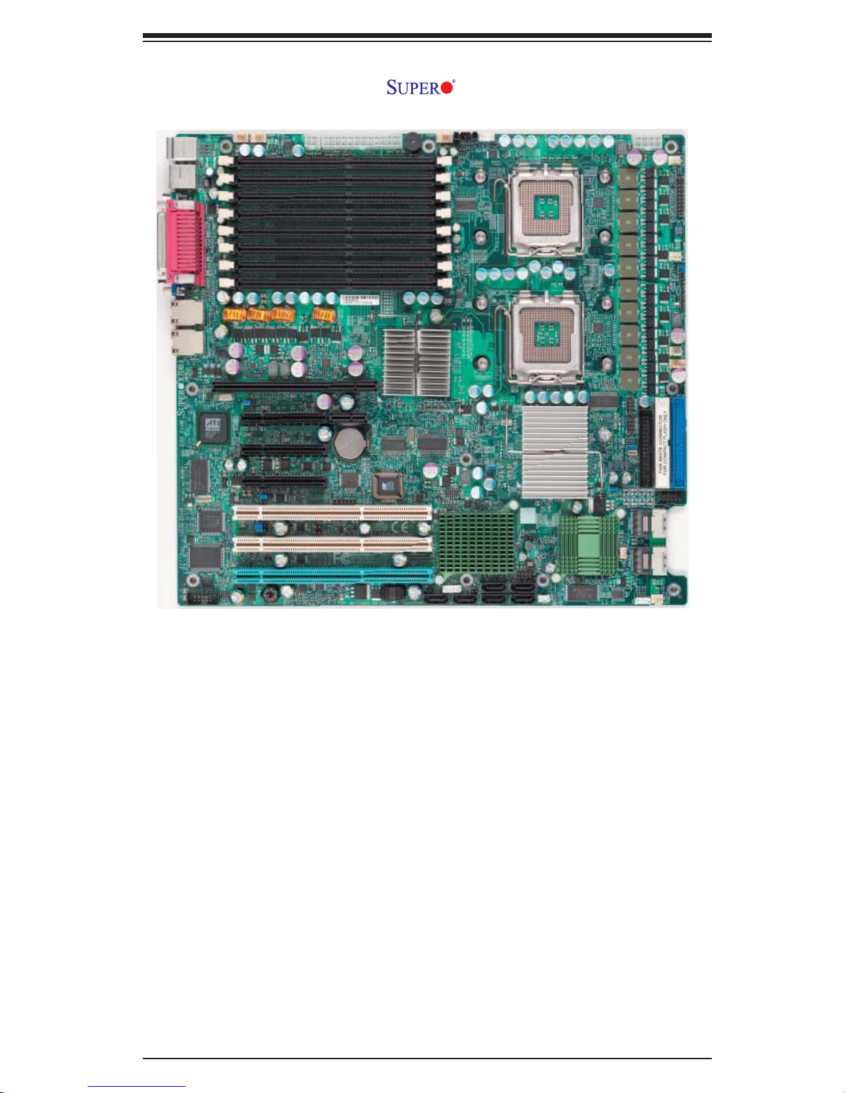
Figure 1-1. X7DB3 Image
Chapter 1: Introduction
*Note: The drawings and pictures shown in this manual were based on the
latest PCB Revision available at the time of publishing of the manual. The
motherboard you’ve received may or may not look exactly the same as the
graphics shown in the manual.
1-3
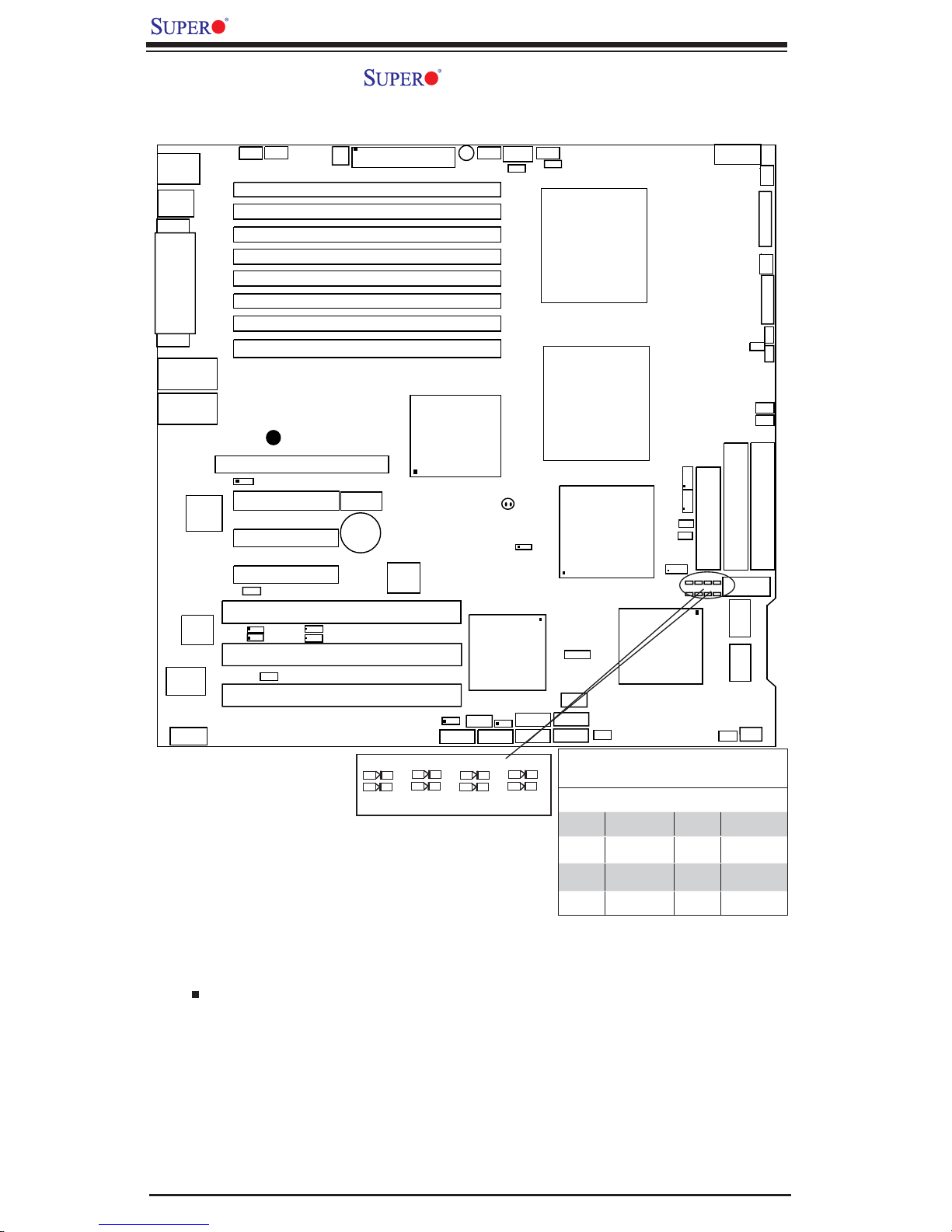
X7DB3 User's Manual
A
Figure 1-2. X7DB3 Motherboard Layout
4-Pin
Fan5
KB/
Mous e
USB 0/1
COM1
Parrallel
A
G
V
GLAN1
GLAN2
S
JCOM2
Port
JLAN1
C
L
T
C
/O
I
S
UP ER
GA
V
R
L
TR
N
A
R
L
R
Slot7
S
JPL1
J
Sl
S
l
P
l
Slot6
Slot5
Slot4
o
L
o
ot
Fan6
3
t
2
2
t
1
JPG1
®
X7DB 3
SIMLP IPMI
PCI-Exp x8
Exp
PCI-
PCI-Exp x4
WD
J
33 MH
X1
-
I
PC
J28
J27
3
1
X
-
I
PC
JWO
PCI-X 100
PWR
DIMM 4B (B ank 4)
D
D
D
DIM
DIMM 2A (B ank 2)
DI
D
x
MH
3
R
MH
24-Pin
IMM 4A (
IM
M3B (Ban
I
MM 3A
M
2
B
M
M1B (Ban
IMM 1A (
SEPC
Batter
8
z
z
zZCR
ct#4
Act#0
B
(
Bank 3)
(B ank 2)
B
y
(not drawn to scale)
SMBPS
tel
h
J
S
Buzzer
5000P
id
r
B
K
1
0
A
AT
Act#6
Act#2
ge
SMB
Fan7
AT
S
JAR
J
PXH
JL
1
1
A
Act#7
Act#3
BT
7
J
SATA
SATA
ATX PWR
ank 4)
k3)
k1)
ank 1)
BIOS
Act#5
Act#1
n
I
Nort
PSF
J3P
Xeon Dual C ore
1
U
CP
lCore
a
u
D
n
o
Xe
CPU2
PIO2
SG
1
SAS CTRLR
Adaptec 9410W
I
S
3
/
OL
W
4
2
USB 4
US
SATA
SATA
2
B
5
3
PIO1
SG
1
CF
J
F1
W
J
1
S
P
J
B2
S
E
tel
n
dge
i
r
B
h
t
u
o
Onboard SAS_Activity_LED Indica-
tors (*Note: Act=Active)
Act# Defi nition Act# Defi nition
Act#0 SAS0:Act Act#4 SAS4:Act
Act#1 SAS1:Act Act#5 SAS5:Act
8-pinPW R
Floppy
BPLED
4-7
S
SA
0-3
S
SA
A
JS
h
s
Fla
t
c
a
p
Com
3
L
Fan4
1
n
a
F
FP Control
an2
F
SPK
PW LED
JP1
E
1
JOH1
F
an
3
8
n
a
F
1
IDE
n
Co
Notes:
1. Jumpers not indicated are for test purposes only.
2. See Chapter 2 for detailed information on jumpers, I/O ports and
JF1 front panel connections.
3. " " indicates the location of Pin 1.
4. SEPC: Super Micro Enhanced Power Connector, specially designed to support
Super Micro 2U Riser Card only.
5. LE 1 is the 5V Standby Power LED Indicator. When LE1 is off, the system is
off. When the green light is on, the system is on. When the yellow light is on, the
system is off, but the AC power cable is still connected. Make sure to disconnect
the power cable before removing or installing components.
6. For the ZCR card to function properly, be sure to install it in the green slot.
Act#2 SAS2:Act Act#6 SAS6:Act
Act#3 SAS3:Act Act#7 SAS7:Act
1-4

Chapter 1: Introduction
Quick Reference ( X7DB3)
Jumper Description Default Setting
27, J28 I
J3P 3rd PWR Failure Detect Open (Disabled)
JBT1 CMOS Clear See Chapter 2
JCF1 Compact Card Master/Slave Select On (Master)
JPG1 VGA Enable Pins 1-2 (Enabled)
JPL1/ JPL2 GLAN1/GLAN2 Enable Pins 1-2 (Enabled)
JPS1 SAS Controller Enable Pins 1-2 (Enabled)
JWD Watch Dog Pins 1-2 (Reset)
Connector Description
ATX PWR (JPW1) Primary 24-Pin ATX PWR Connector
Aux. PWR/CPU PWR +12V 4-pin PWR (JWP2)/+12V 8-pin PWR(JPW3)
ACT#0-ACT#7 SAS Activity LED Indicators (See Page 1-4)
Alarm Reset (JAR) Alarm Reset (*Open: normal)
BP LED Connector(JSLED1) Back Panel Activity LED Connector
Chassis Intrusion (JL1) Chassis Intrusion Header
COM1/COM2 COM1/COM2 Serial Port Connector/Header
Compact PWR(JWF1) Compact Card PWR Connector (*Used if JCF1 is on.)
DIMM#1A-DIMM#4B Memory DDRII Slots
FAN 1-8 Fans 1-8 (CPU Fans/Chassis Fans)
Floppy (J22) Floppy Disk Drive Connector
FP CTRL (JF1) Front Control Panel Connector
GLAN 1/2 (JLAN1/2) G-bit Ethernet Ports
IDE1/IDE2 (*Note) IDE1 Hard Drive (JIDE1)/Compact Flash Card (JIDE2)
Keylock (JK1) Keylock Header
OH LED (JOH1) Overheat LED
Parallel (J21) Parallel (Printer) Port
PSF Power Supply Failure (See Chapter 2)
PWR LED (LE1) PWR LED Indicator (*Note 5 on Pg.1-4)
PWR LED/SPKR (JD1) PWR LED(pins1-3)/SpeakerHeader (pins 4-7)
PWR SMB (J17) Power System Management (I
SATA0-SATA5 Intel SATA 0-5 Connectors
SAS 0-3, SAS 4-7 SAS Connectors 0-3 (JSA1), SAS 4-7 (JSA2)
SGPIO 1/2(J29,J30) Serial General Purpose Input/Output Headers
SMB (J18) System Management Bus Header
Slot 7 SIM Low Profi le IPMI Connector
USB 0/1,USB 2/3, USB4 Back Panel USB 0/1, Front Panel USB 2/3, FP USB4
VGA (J15) VGA Connector
WOL (JWOL) Wake-on-LAN Header
WOR (JWOR) Wake-on-Ring Header
2
C Bus to PCI-X/PCI-E Slots Open (Disabled)
2
C) Header
*Note: JIDE2 is for Compact Card Use only. For Compact Card to work properly,
please enable JCF1 by putting cap on it and connect JWF1 to a power supply.
1-5

X7DB3 User's Manual
Motherboard Features
CPU
• Dual Intel
®
64-bit Xeon LGA 771 quad core/dual core processors at a front side
bus speed of 1.333 GHz/1.066 GHz/677 MHz with a system clock speed of
333/267/166 MHz
Memory
• Eight 240-pin DIMM sockets with support up to 32 GB DDR2 Fully Buffered
(FBD) ECC 667/533 Memory (*See Section 2-3 in Chapter 2 for DIMM Slot
Population.)
Chipset
• Intel 5000P chipset, including: the 5000P Memory Control Hub (MCH), the En-
terprise South Bridge 2 (ESB2), and the I/O subsystem (PXH).
Expansion Slots
• Three PCI-Express slots (*two slots at x8@4GB/sec, one slot x4@2GB/sec. on
x8 connector)
• Three 64-bit PCI-X slots (*two PCI-X-133 slots, one PCI-X-100 w/ZCR slot)
• One SPEC slot (*for Super Micro's 2U Active Riser cards)
BIOS
• 8 Mb Phoenix
®
Flash ROM
• DMI 2.3, PCI 2.2, ACPI 1.0, ACPI 2.0, Plug and Play (PnP), SMBBIOS 2.3
PC Health Monitoring
• Onboard voltage monitors for CPU cores, chipset voltage, +1.8V, +3.3V, +5V,
+12V, −12V, +3.3V Standby, and +5V standby
• Fan status monitor with fi rmware control
• CPU/chassis temperature monitors
• CPU fan auto-off in sleep mode
• CPU slow-down on temperature overheat
• CPU thermal trip support for processor protection, power LED
• Power-up mode control for recovery from AC power loss
• Auto-switching voltage regulator for CPU cores
• System overheat/Fan Fail LED Indicator and control
• Chassis intrusion detection
• System resource alert via Supero Doctor III
• Low noise fan speed control
• Pulse Width Modulated (PWM) fan control
• I2C temperature sensing monitoring
1-6

Chapter 1: Introduction
• Thermal Monitor 2 (TM2) support
• Intel Virtualization Technology support
• PECI (Platform Enhancement Confi guration Interface) ready
ACPI Features
• Slow blinking LED for suspend state indicator
• Main switch override mechanism
• ACPI Power Management
Onboard I/O
• Adaptec AIC 9410 SAS Controller supports eight SAS ports (RAID 0, 1,10)
• Six SATA 3.0Gbps ports (RAID 0, 1,10, 5 for the Windows OS)
• One ZCR slot supports Super Micro's LPZCR2 Add-on card (*optional for
SAS)
• One SIMLP IPMI Slot
• Intel 82563 Gigabit Ethernet controller supporting two Giga-bit LAN ports
• Two EIDE Ultra DMA/100 bus master interfaces supporting one IDE (the blue
slot) and one Compact Flash card (the white slot)
• Two SGPIO (Serial General Purpose Input/Output) headers with support for
ESB2 SATA
• One fl oppy port interface
• Two COM ports (1 header, 1 port)
• One EPP/ECP Parallel Port
• One VGA Port
• PS/2 mouse and PS/2 keyboard ports
• Up to fi ve USB 2.0 (Universal Serial Bus) (2 ports, 3 Headers)
• ATI 16 MB ES1000 Graphic Controller
• Super I/O: Winbond W83627HF w/Hardware Monitor support: W83793,
HECETA
Other
• External modem ring-on
• Wake-on-LAN (WOL)
• Wake-on-Ring (WOR)
• Console redirection
• Onboard Fan Speed Control by Thermal Management via BIOS
CD/Diskette Utilities
• BIOS fl ash upgrade utility and device drivers
Dimensions
• ATX Ext. 12" x 13.05" (304.8 x 331.5 mm)
1-7
X7DB3 User's Manual
J13
#2
J5
#6
PCI - E XP X8 SLOT
SEPC
PCI - EXP
PCI - EXP
PCI - X 133
PCI 3 3
PROCESSOR#2
1333
1067/
/S
MT
PCI - EXP X8
PCI -EX
P
X8
X4
PORT
#0
X8
PORT
#1, 2
MMZ
PORT
#4, 5
MCH
PORT
#6, 7
PORT PORT
PORT PORT
#4 #3
VRM
I SL6307
J6
#5
J9
#4
2
J1
#1
AIC
9410W
PCI - X SL OT
PCI - X SL OT zcr
4
J1
#3
PCI - X 133
PCI - X
VGA
CONN
PCI - X SL OT
EXP X8 SLOT
I-
PC
A
B
133
VGA
ES 1000
PX
PCI - E XP X8 SLOT
H
5000P
#0#2, 3
PCI E X8
ESB2
PROCESSOR#1
1067/1333
/S
MT
FBD CHNL0
FBD CHNL1
D CH NL 2
FB
CHNL 3
FBD
PCI E X4
AT A 100
EXP. BUS
3. 0 Gb/ S
USB 2.0
#1A
F B D DIMM
#0
#0
#1B
#1
#1
VRM
I SL6307
#2B
#2A
DIMM
FBD
ID
E
CONN
EBUS CONN
#5
#4
#3
#2
SATA
#4
#3
#2
US B
#3A
F B D DI MM
#3B
#4B
#4A
DIMM
FBD
DDR
RJ 4 5
RJ 4 5
PARALLEL
PORT
KUMERAN
GB L A N FWH
GI L GAL
FDD
SI O
W83627
HF
MS
KB
COM1
COM2
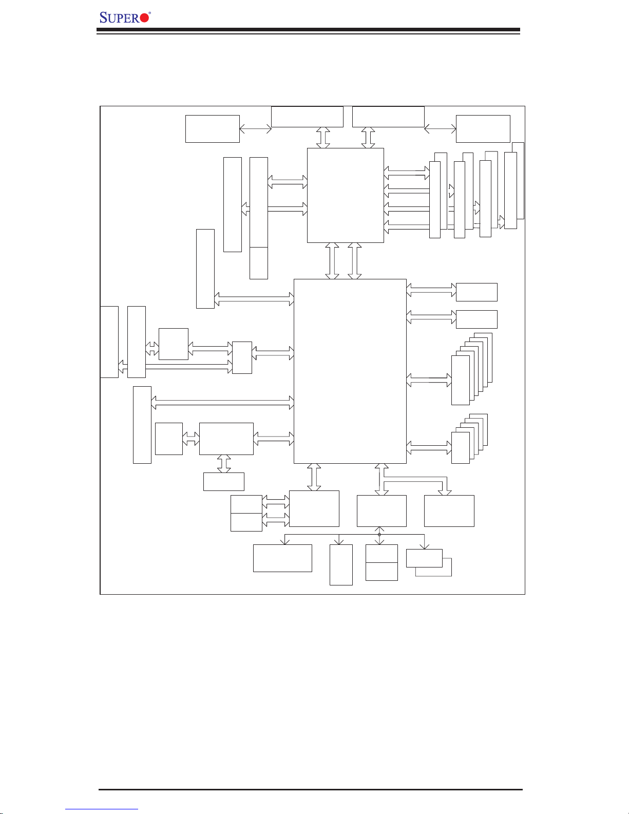
Figure 1-9. Block Diagram of the 5000P Chipset
Note: This is a general block diagram. Please see the previous Motherboard Features
pages for details on the features of each motherboard.
LPC
1-8

Chapter 1: Introduction
1-2 Chipset Overview
Built upon the functionality and the capability of the 5000P chipset, the X7DB3
motherboard provides the performance and feature set required for dual pro-
cessor-based servers with confi guration options optimized for communications,
presentation, storage, computation and database applications. The 5000P chipset
supports single or dual 64-bit quad core/dual core processor(s) with front side bus
speeds of up to 1.333 GHz/1.066 GHz/677 MHz. The chipset consists of the 5000P
Memory Controller Hub (MCH), the Enterprise South Bridge 2 (ESB2), and the I/O
subsystem (PXH).
The 5000P MCH chipset is designed for symmetric multiprocessing across two inde-
pendent front side bus interfaces. Each front side bus uses a 64-bit wide, 1333 MHz
data bus that transfers data at 10.7 GB/sec. (for a total bandwidth of 21.3GB/sec.).
The MCH chipset connects up to eight Fully Buffered DIMM modules, providing
a total memory bandwidth of 32 GB/s for DDR2 533/667. The MCH chipset also
provides one x8 PCI-Express and one x4 ESI interfaces to the ESB2. In addition,
the 5000P chipset offers a wide range of RAS features, including memory interface
ECC, x4/x8 Single Device Data Correction, CRC, parity protection, memory mirror-
ing and memory sparing.
The Xeon Quad core/dual core Processor Features
Designed to be used with conjunction of the 5000P chipset, the Xeon quad core/dual
core Processor provides a feature set as follows:
The Xeon Quad core/dual core Processors
*L1 Cache Size: Instruction Cache (32KB/16KB), Data Cache (32KB/24KB)
*L2 Cache Size: 4MB/2MB (per core)
*Data Bus Transfer Rate: 8.5 GB/s
*Package: FC-LGA6/FC-LGA4, 771 Lands
1-9

X7DB3 User's Manual
1-3 Special Features
Recovery from AC Power Loss
BIOS provides a setting for you to determine how the system will respond when
AC power is lost and then restored to the system. You can choose for the system
to remain powered off (in which case you must hit the power switch to turn it back
on), or for it to automatically return to power-on state, or you can also choose for
it to automatically return to the last state prior to power loss. See the Power Lost
Control setting in the Advanced BIOS Setup section (Boot Features) to change
this setting.
1-4 PC Health Monitoring
This section describes the PC health monitoring features of the X7DB3. All have an
onboard System Hardware Monitor chip that supports PC health monitoring.
Onboard Voltage Monitors for +1.5V,+1.8V, +3.3V, +5V, +12V, −12V,
+3.3V Standby, and +5V standby
An onboard voltage monitor will scan these voltages continuously. Once a
voltage becomes unstable, a warning is given or an error message is sent to
the screen. Users can adjust the voltage thresholds to defi ne the sensitivity
of the voltage monitor.
Fan Status Monitor with Firmware Control
The PC health monitor can check the RPM status of the cooling fans. The onboard
CPU and chassis fans are controlled by Thermal Management via BIOS (under the
Hardware Monitoring section in the Advanced BIOS Setup section.)
Environmental Temperature Control
The thermal control sensor monitors the CPU temperature in real time and will turn
on the thermal control fan whenever the CPU temperature exceeds a user-defi ned
threshold. The overheat circuitry runs independently from the CPU. Once it detects
that the CPU temperature is too high, it will automatically turn on the thermal fan
control to prevent any overheat damage to the CPU. The onboard chassis thermal
circuitry can monitor the overall system temperature and alert users when the chas-
sis temperature is too high.
1-10

Chapter 1: Introduction
CPU Fan Auto-Off in Sleep Mode
The CPU fan activates when the power is turned on. It continues to operate when
the system enters Standby mode. When in sleep mode, the CPU will not run at
full power, thereby generating less heat.
CPU Overheat LED and Control
This feature is available when the user enables the CPU overheat warning function
in the BIOS. This allows the user to defi ne an overheat temperature. When this tem-
perature is exceeded, both the overheat fan and the warning LED are triggered.
System Resource Alert
This feature is available when used with Supero Doctor III in the Windows OS
environment or used with Supero Doctor II in Linux. Supero Doctor is used to
notify the user of certain system events. For example, if the system is running
low on virtual memory and there is insuffi cient hard drive space for saving the
data, you can be alerted of the potential problem. You can also confi gure Supero
Doctor to provide you with warnings when the system temperature goes beyond
a pre-defi ned range.
1-5 ACPI Features
ACPI stands for Advanced Confi guration and Power Interface. The ACPI specifi -
cation defi nes a fl exible and abstract hardware interface that provides a standard
way to integrate power management features throughout a PC system, including its
hardware, operating system and application software. This enables the system to
automatically turn on and off peripherals such as CD-ROMs, network cards, hard
disk drives and printers. This also includes consumer devices connected to the PC
such as VCRs, TVs, telephones and stereos.
In addition to enabling operating system-directed power management, ACPI
provides a generic system event mechanism for Plug and Play and an operating
system-independent interface for confi guration control. ACPI leverages the Plug
and Play BIOS data structures while providing a processor architecture-independent
implementation that is compatible with both Windows 2000 and Windows NT 5.0.
This setting is also located in the Advanced BIOS Setup section (Boot Features).
Slow Blinking LED for Suspend-State Indicator
When the CPU goes into a suspend state, the chassis power LED will start blinking
to indicate that the CPU is in suspend mode. When the user presses any key, the
CPU will wake-up and the LED will automatically stop blinking and remain on.
1-11

X7DB3 User's Manual
Main Switch Override Mechanism
When an ATX power supply is used, the power button can function as a system
suspend button to make the system enter a SoftOff state. The monitor will be
suspended and the hard drive will spin down. Pressing the power button again
will cause the whole system to wake-up. During the SoftOff state, the ATX power
supply provides power to keep the required circuitry in the system alive. In case
the system malfunctions and you want to turn off the power, just press and hold
the power button for 4 seconds. This option can be set in the Boot section of the
Advanced BIOS Setup routine.
External Modem Ring-On
Wake-up events can be triggered by a device such as the external modem ringing
when the system is in the SoftOff state. Note that external modem ring-on can only
be used with an ATX 2.01 (or above) compliant power supply.
Wake-On-LAN (WOL)
Wake-On-LAN is defi ned as the ability of a management application to remotely
power up a computer that is powered off. Remote PC setup, up-dates and asset
tracking can occur after hours and on weekends so that daily LAN traffi c is kept to
a minimum and users are not interrupted. The motherboard has a 3-pin header
(WOL) to connect to the 3-pin header on a Network Interface Card (NIC) that has
WOL capability. In addition, an onboard LAN controller can also support WOL
without any connection to the WOL header. The 3-pin WOL header is to be used
with a LAN add-on card only.
*Note: Wake-On-LAN requires an ATX 2.01 (or above) compliant power supply.
1-6 Power Supply
As with all computer products, a stable power source is necessary for proper and
reliable operation. It is even more important for processors that have high CPU
clock rates.
The X7DB3 can only accommodate 24-pin ATX power supplies. Although most
power supplies generally meet the specifi cations required by the CPU, some are
inadequate. In addition, the 12V 4-pin power supply - is also required to ensure
adequate power supply to the system. Also your power supply must supply 1.5A
for the Ethernet ports.
1-12

Chapter 1: Introduction
NOTE: The + 12V 8-pin Aux. Power Connector is always required. Failure to
provide this extra power will result in CPU PWR Failure. See Section 2-5 for
details on connecting the power supply.
It is strongly recommended that you use a high quality power supply that meets ATX
power supply Specifi cation 2.02 or above. It must also be SSI compliant (info at
http://www.ssiforum.org/). Additionally, in areas where noisy power transmission is
present, you may choose to install a line fi lter to shield the computer from noise. It
is recommended that you also install a power surge protector to help avoid problems
caused by power surges.
1-7 Super I/O
The disk drive adapter functions of the Super I/O chip include a fl oppy disk drive
controller that is compatible with industry standard 82077/765, a data separator,
write pre-compensation circuitry, decode logic, data rate selection, a clock genera-
tor, drive interface control logic and interrupt and DMA logic. The wide range of
functions integrated onto the Super I/O greatly reduces the number of components
required for interfacing with fl oppy disk drives. The Super I/O supports 360 K, 720
K, 1.2 M, 1.44 M or 2.88 M disk drives and data transfer rates of 250 Kb/s, 500 Kb/s
or 1 Mb/s. It also provides two high-speed, 16550 compatible serial communication
ports (UARTs. Each UART includes a 16-byte send/receive FIFO, a programmable
baud rate generator, complete modem control capability and a processor interrupt
system. Both UARTs provide legacy speed with baud rate of up to 115.2 Kbps
as well as an advanced speed with baud rates of 250 K, 500 K, or 1 Mb/s, which
support higher speed modems.
The Super I/O supports one PC-compatible printer port (SPP), Bi-directional Printer
Port (BPP) , Enhanced Parallel Port (EPP) or Extended Capabilities Port (ECP).
The Super I/O provides functions that comply with ACPI (Advanced Confi guration
and Power Interface), which includes support of legacy and ACPI power manage-
ment through an SMI or SCI function pin. It also features auto power management
to reduce power consumption.
1-13

X7DB3 User's Manual
Notes
1-14

Chapter 2: Installation
Chapter 2
Installation
2-1 Static-Sensitive Devices
Electric-Static-Discharge (ESD) can damage electronic com ponents. To prevent
damage to your system board, it is important to handle it very carefully. The following
measures are generally suffi cient to protect your equipment from ESD.
Precautions
• Use a grounded wrist strap designed to prevent static discharge.
• Touch a grounded metal object before removing the board from the antistatic
bag.
• Handle the board by its edges only; do not touch its components, peripheral
chips, memory modules or gold contacts.
• When handling chips or modules, avoid touching their pins.
• Put the motherboard and peripherals back into their antistatic bags when not in
use.
• For grounding purposes, make sure your computer chassis provides excellent
conductivity between the power supply, the case, the mounting fasteners and
the motherboard.
• Use only the correct type of onboard CMOS battery as specifi ed by the manu-
facturer. Do not install the onboard battery upside down to avoid possible explo-
sion.
Unpacking
The motherboard is shipped in antistatic packaging to avoid static damage. When
unpacking the board, make sure the person handling it is static protected.
2-1
X7DB3 User's Manual
2-2 Processor and Heatsink Fan Installation
When handling the processor package, avoid placing
direct pressure on the label area of the fan.
(*Notes: 1. Always connect the power cord last and always remove it before adding,
removing or changing any hardware components. Make sure that you install the
processor into the CPU socket before you install the CPU heatsink.
2. Intel's boxed Xeon CPU package contains the CPU fan and heatsink assembly.
If you buy a CPU separately, make sure that you use only Intel-certifi ed multi-di-
rectional heatsink and fan.
3. Make sure to install the motherboard into the chassis before you install the CPU
heatsink and fan.)
4. When purchasing an LGA 771 CPU or when receiving a motherboard with an LGA
771 CPU pre-installed, make sure that the CPU plastic cap is in place and none of
the CPU pins are bent; otherwise, contact the retailer immediately.
5. Refer to the MB Features Section for more details on CPU support.
!
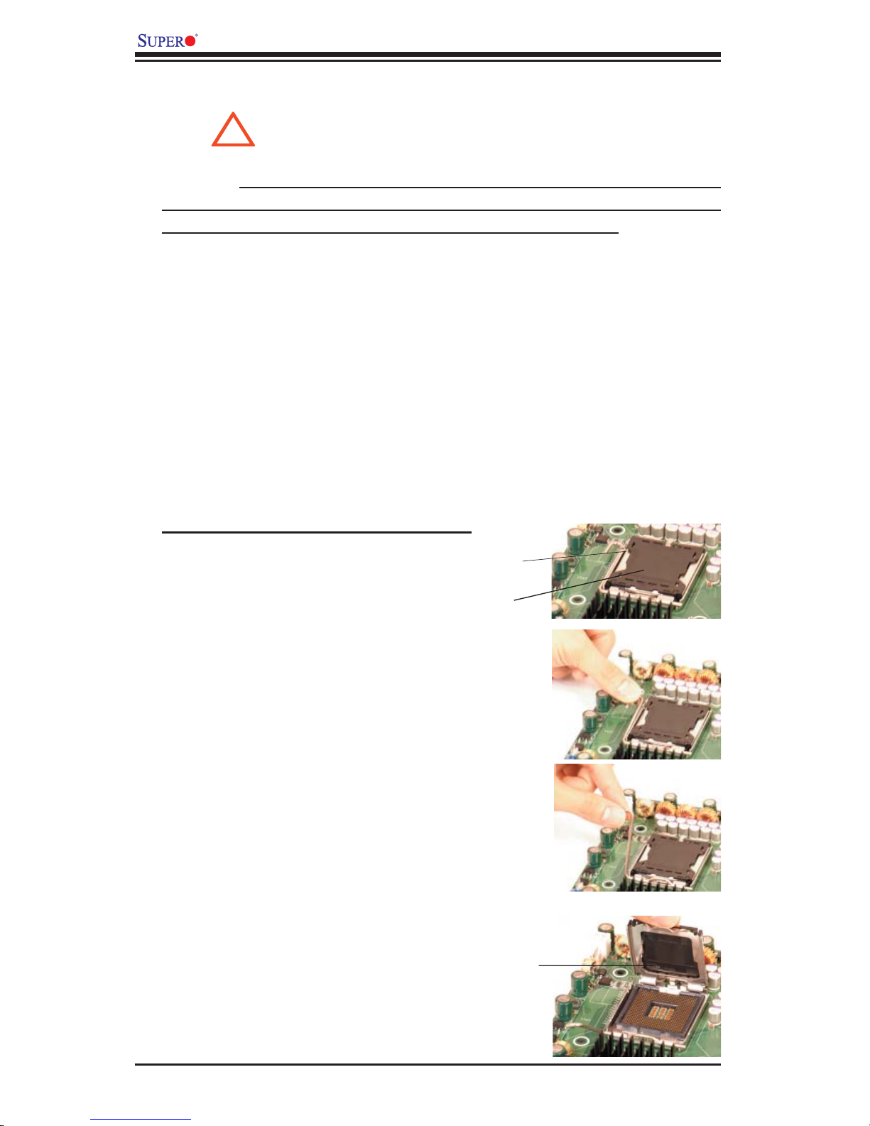
Installation of the LGA771 Processor
1. Press the socket clip to release
the load plate, which covers the CPU
socket, from its locking position.
2. Gently lift the socket clip to open
the load plate.
Socket Clip
Load Plate
Load Plate
2-2
Chapter 2: Installation
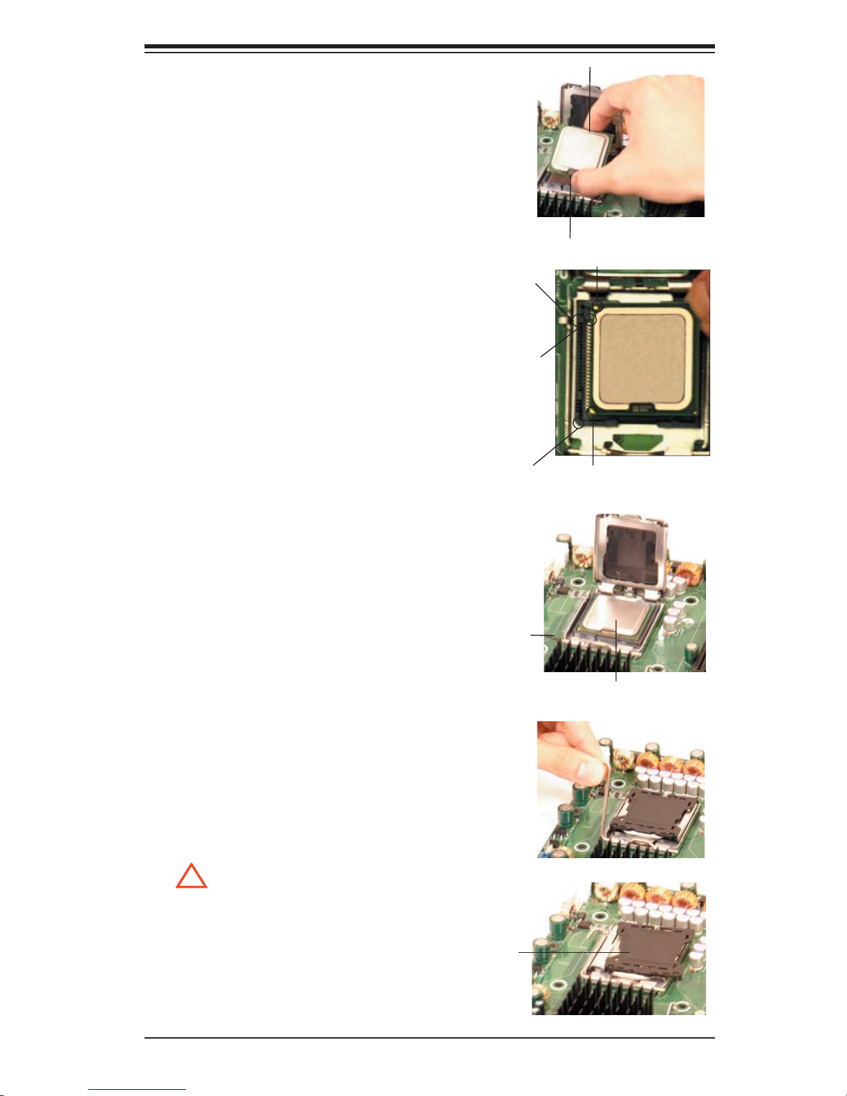
3. Use your thumb and your index
fi nger to hold the CPU at the North
Center Edge and the South Center
Edge of the CPU.
4. Align CPU Pin1 (the CPU corner
marked with a triangle) against the
socket corner that is marked with a
triangle cutout.
5. Align the CPU key that is the
semi-circle cutout below a gold dot
against the socket key, the notch on
the same side of the triangle cutout
on the socket.
6. Once aligned, carefully lower the
CPU straight down to the socket.
(**Do not drop the CPU on the
socket. Do not move the CPU hori-
zontally or vertically. Do not rub the
CPU against the surface or against
any pins of the socket to avoid dam-
age to the CPU or the socket.)
Socket Key
(Socket Notch)
CPU Key (semi-
circle cutout)
below the circle.
Corner with a
triangle cutout
North Center Edge
South Center Edge
gold dot
CPU Pin1
7. With the CPU inside the socket,
inspect the four corners of the CPU
to make sure that the CPU is prop-
erly installed.
8. Use your thumb to gently push the
socket clip down to the clip lock.
9. If the CPU is properly installed
into the socket, the plastic cap will
be automatically released from the
load plate when the clip is pushed in
the clip lock. Remove the plastic cap
from the motherboard.
!
(*Warning: Please save the
plastic cap. The motherboard must
be shipped with the plastic cap
properly installed to protect the CPU
socket pins. Shipment without the
plastic cap properly installed will
cause damage to the socket pins.)
Socket clip
CPU in the CPU socket
Plastic cap
is released
from the
load plate
if the CPU
is properly
installed.
2-3
X7DB3 User's Manual
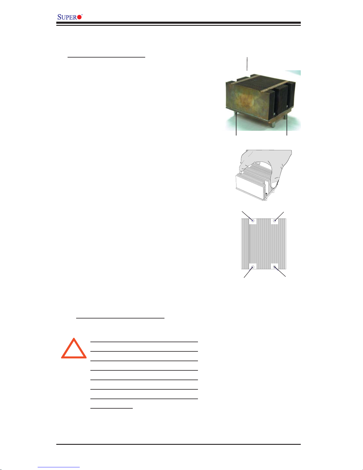
Installation of the Heatsink
CEK Heatsink Installation
1. Do not apply any thermal grease to
the heatsink or the CPU die-the required
amount has already been applied.
2. Place the heatsink on top of the
CPU so that the four mounting holes
are aligned with those on the retention
mechanism.
3. Screw in two diagonal screws (ie the
#1 and the #2 screws) until just snug (-do
not fully tighten the screws to avoid pos-
sible damage to the CPU.)
4. Finish the installation by fully tightening
all four screws.
CEK Passive Heatsink
Screw#1 Screw#2
Screw#1
Screw#4
To Un-install the Heatsink
(Warning: We do not recommend
!
that the CPU or the heatsink be
removed. However, if you do need
to uninstall the heatsink, please
follow the instructions below to
uninstall the heatsink to prevent
damage done to the CPU or the
CPU socket.)
Screw#3
Screw#2
2-4
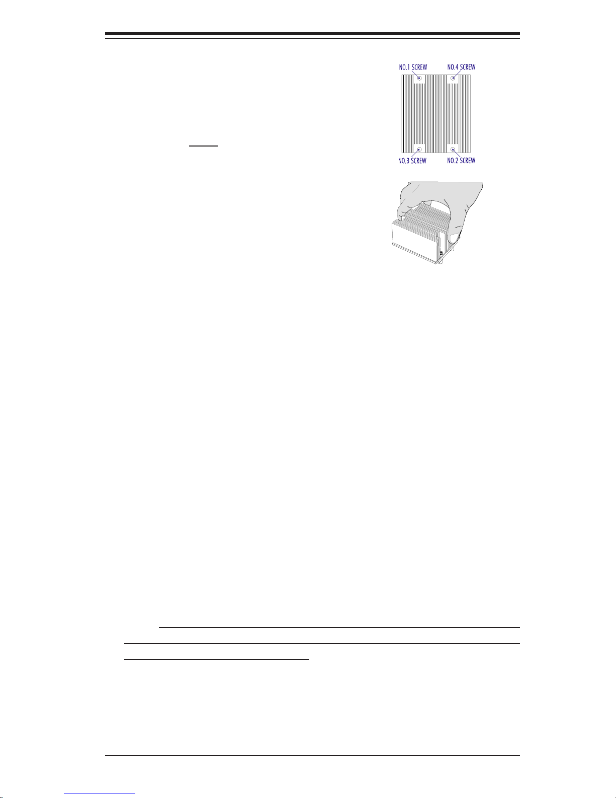
1. Unscrew and remove the heatsink screws
from the motherboard in the sequence as show
in the picture on the right.
2. Hold the heatsink as shown in the picture
on the right and gently wriggle the heatsink to
loosen it from the CPU. (Do not use excessive
force when wriggling the heatsink!!)
3. Once the CPU is loosened, remove the
heatsink from the CPU socket.
4. Clean the surface of the CPU and the
heatsink to get rid of the old thermal grease.
Reapply the proper amount of thermal grease
on the surface before you re-install the CPU
and the heatsink.
Chapter 2: Installation
Mounting the Motherboard in the Chassis
All motherboards have standard mounting holes to fi t different types of chas-
sis. Make sure that the locations of all the mounting holes for both motherboard
and chassis match. Make sure that the metal standoffs click in or are screwed in
tightly. Then, use a screwdriver to secure the motherboard onto the motherboard
tray. (*Note: some components are very close to the mounting holes. Please take
precautionary measures to prevent damage done to these components when you
install the motherboard to the chassis.)
2-5
X7DB3 User's Manual
2-3 Installing DIMMs
Note: Check the Super Micro web site for recommended memory modules.
CAUTION
Exercise extreme care when installing or removing DIMM
modules to prevent any possible damage. Also note that the
memory is interleaved to improve performance (see step 1).
DIMM Installation (See Figure 2-2)
1. Insert the desired number of DIMMs into the memory slots, starting with DIMM
#1A. The memory scheme is interleaved so you must install two modules at
a time, beginning with DIMM #1A, then DIMM #2A and so on. (Please see the
Memory Installation Table below.)
2. Insert each DIMM module vertically into its slot. Pay attention to the notch along
the bottom of the module to prevent inserting the DIMM module incorrectly.
3. Gently press down on the DIMM module until it snaps into place in the slot.
Repeat for all modules (see step 1 above).
Memory Support
The X7DB3 supports up to 32 GB fully buffered (FBD) ECC DDR2 533/667 in 8
DIMMs. Populating DIMM modules with pairs of memory modules of the same size
and same type will result in Interleaved Memory which will increase memory
performance.
*Note 1: Due to OS limitations, some operating systems may not show more than
4 GB of memory.
Optimized DIMM Population Configurations
Branch0 Branch1
Number of
DIMMs
2 DIMMs 1A ------ 2A ------ ------ ------ ------ -----4 DIMMs 1A ------ 2A ------ 3A ------ 4A -----6 DIMMs 1A 1B 2A 2B 3A ------ 4A -----8 DIMMs 1A 1B 2A 2B 3A 3B 4A 4B
Bank 1
(Channel 0)
Bank 2
(Channel 1)
Bank 3
(Channel 2)
Bank 4
(Channel 3)
(*Notes: i. DIMM slot# specified: DIMM slot to be populated; “---“: DIMM slot not to
be populated. ii. Both FBD 533 MHz and 667MHz DIMMs are supported; however,
you need to use the memory modules of the same speed and of the same type on a
motherboard. iii. Interleaved memory is supported when pairs of DIMM modules are
installed. To optimize memory performance, please install pairs of DIMMs in both
Branch 0 and Branch 1. iv. For memory to work properly, you need to follow the
restrictions listed above. )
*Note 2: Due to memory allocation to system devices, memory remaining avail-
able for operational use will be reduced when 4 GB of RAM is used. The reduction
in memory availability is disproportional. (Refer to the following Memory Availability
Table for details.)
2-6
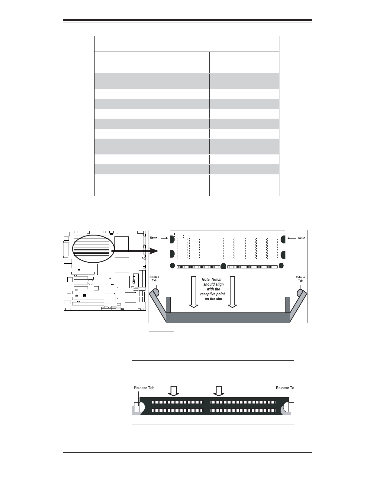
Possible System Memory Allocation & Availability
Chapter 2: Installation
System Device Size Physical Memory
Remaining (-Available)
(4 GB Total System Memory)
Firmware Hub fl ash memory (System
1 MB 3.99
BIOS)
Local APIC 4 KB 3.99
Area Reserved for the chipset 2 MB 3.99
I/O APIC (4 Kbytes) 4 KB 3.99
PCI Enumeration Area 1 256 MB 3.76
PCI Express (256 MB) 256 MB 3.51
PCI Enumeration Area 2 (if needed)
512 MB 3.01
-Aligned on 256-MB boundary-
VGA Memory 16 MB 2.85
TSEG 1 MB 2.84
Memory available to OS and other ap-
2.84
plications
Figure 2-2. Installing and Removing DIMMs
JLAN1
®
3
B
7D
X
S
ER
P
U
To Remove:
Use your thumbs
to gently push
the release tabs
near both ends of
the module. This
should release it
from the slot.
DDR2 FBD
To Install: Insert module vertically and press down until it
snaps into place. Pay attention to the alignment notch at
the bottom.
Top View of DDR2 FBD Slot
2-7
X7DB3 User's Manual
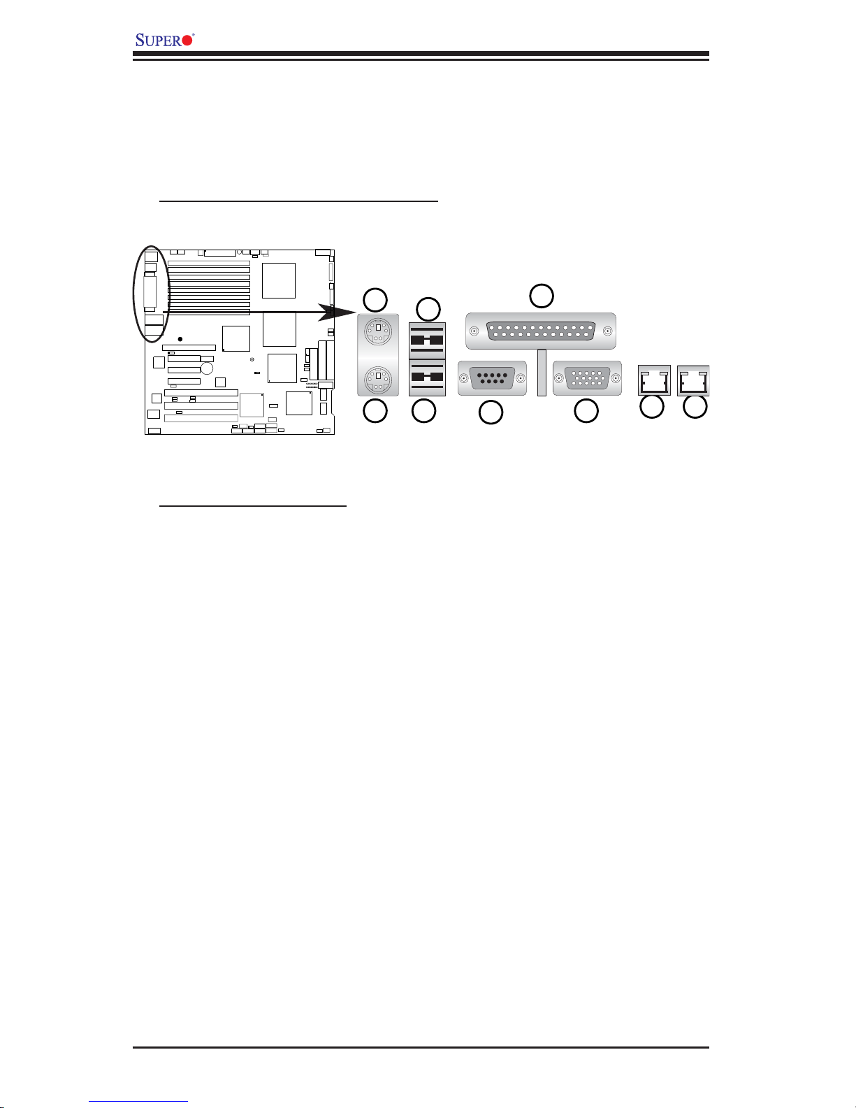
2-4 Control Panel Connectors/IO Ports
The I/O ports are color coded in conformance with the PC 99 specifi cation. See
Figure 2-3 below for the colors and locations of the various I/O ports.
A. Back Panel Connectors/IO Ports
JLAN1
®
3
X7DB
S
R
E
P
U
2
1
4
3
5
7
6
Figure 2-3. Back Panel I/O Port Locations and Defi nitions
Back Panel Connectors
1. Keyboard (Purple)
2. PS/2 Mouse (Green)
3. Back Panel USB Port 0
4. Back Panel USB Port 1
5. COM Port 1 (Turquoise)
6. VGA Port (Blue)
7. Parallel Port (Printer)
8. Gigabit LAN 1
9. Gigabit LAN 2
8 9
(*See Section 2-5 for details.)
2-8
Chapter 2: Installation
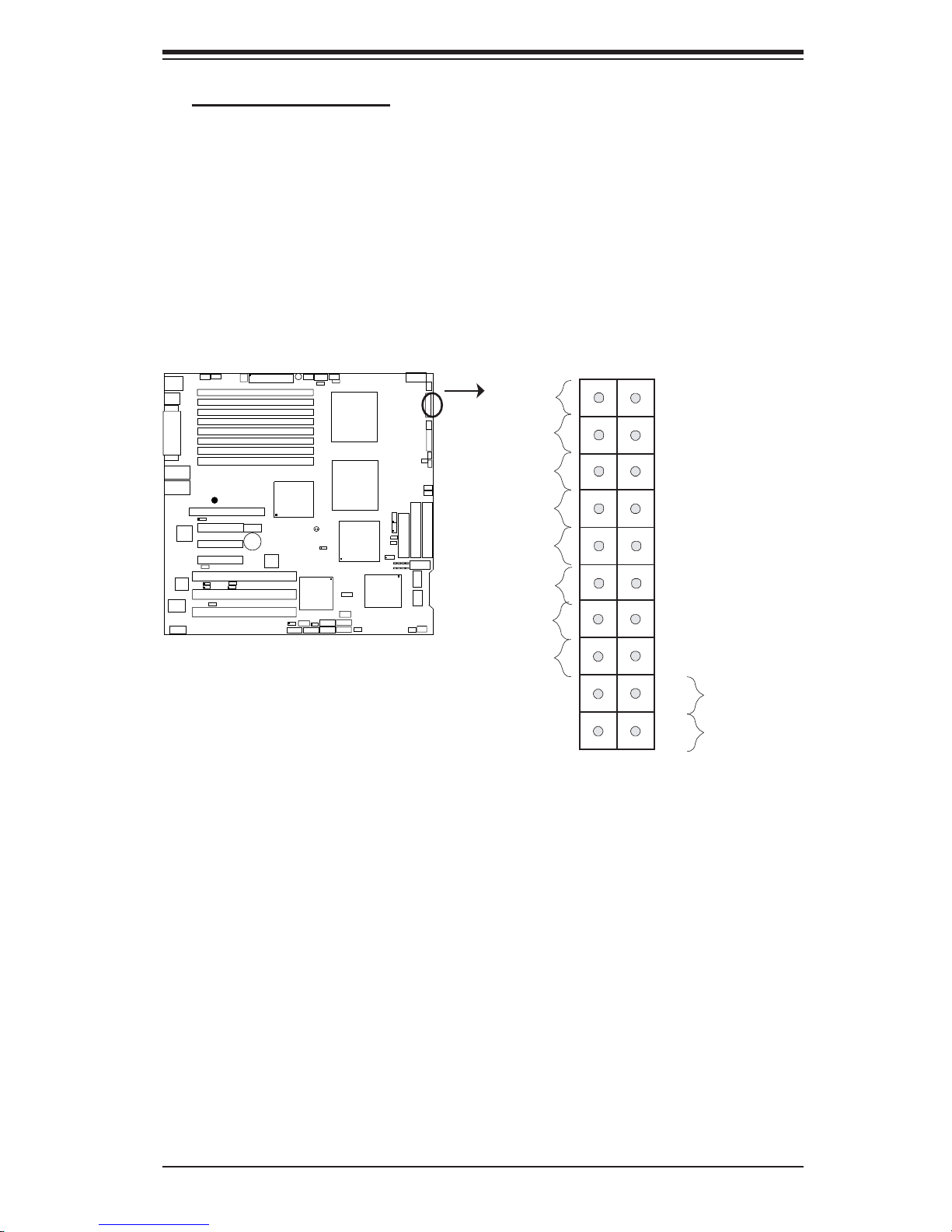
B. Front Control Panel
JF1 contains header pins for various buttons and indicators that are normally
located on a control panel at the front of the chassis. These connectors are de-
signed specifi cally for use with Super Micro server chassis. See Figure 2-4 for the
descriptions of the various control panel buttons and LED indicators. Refer to the
following section for descriptions and pin defi nitions.
Figure 2-4. JF1 Header Pins
1920
Ground
NMI
JLAN1
X
Power LED
®
7DB3
X
S
PER
U
HDD LED
NIC1 LED
NIC2 LED
OH/Fan Fail LED
PWR Fail LED
Ground
Ground
2
1
X
Vcc
Vcc
Vcc
Vcc
Vcc
Vcc
Reset
PWR
Reset Button
Power Button
2-9
X7DB3 User's Manual
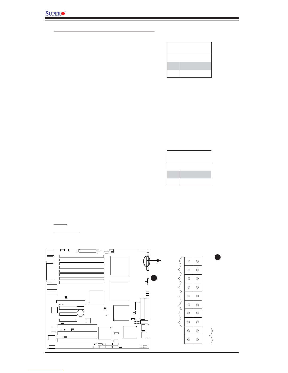
C. Front Control Panel Pin Defi nitions
NMI Button
The non-maskable interrupt button
header is located on pins 19 and 20
of JF1. Refer to the table on the right
for pin defi nitions.
Power LED
The Power LED connection is located
on pins 15 and 16 of JF1. Refer to the
table on the right for pin defi nitions.
NMI Button
Pin Defi nitions (JF1)
Pin# Defi nition
19 Control
20 Ground
Power LED
Pin Defi nitions (JF1)
Pin# Defi nition
15 +5V
16 Ground
A. NMI
B. PWR LED
Fan
KB/
ouse
M
USB 0/1
1
M
CO
Port
Parrallel
JLAN1
VGA
GLAN1
GLAN2
S
UPER
t7
o
l
S
t6
o
l
S
A
VG
LR
TR
C
t5
o
l
S
4
t
o
l
S
t3
o
l
S
LAN
1
PL
J
CTRLR
2
L
P
J
t2
o
l
S
O
/
I
S
1
t
o
l
S
2
M
JCO
Fan5
6
SIMLP IPMI
G1
P
J
PCI-Exp x8
PCI
PCI-Exp x4
D
W
J
-
I
C
P
-
I
C
P
-
I
C
P
®
X7DB3
-Ex p x8
3
3
1
X
J28
J27
3
3
1
X
R
JWO
0
0
1
X
n
i
4-P
R
W
P
DIMM
D
IM
M4
DIMM3B (Bank3
D
I
M
DIMM2B (Bank2
DIMM2
DIMM1B (Ba
D
I
M
z
H
M
z
H
M
z
H
M
24-
4
B(Bank4)
A(Ba
M3
A(Ba
A(Ba
M1
A(Ba
SEPC
ttery
a
B
R
C
Z
P
X
AT
n
i
P
nk 4
n
k
nk 2
nk 1)
nk 1
S
O
I
B
WR
Buzzer
)
)
3
)
)
)
J3P
JAR
ore
ualC
on D
Xe
1
U
P
C
)
ore
ualC
D
n
Xeo
2
U
P
P
0
0
l50
Inte
idge
r
B
h
t
Nor
X
P
SMB
JK
1
JL1
0
A
A
T
T
A
A
S
S
C
1
T
JB
SAS CTRLR
Adaptec 9410W
J7
4
B
S
U
H
/3
SB2
U
4
5
A
A
T
T
A
A
S
S
OL
W
3
2
A
A
T
T
A
A
S
S
1
J
lESB2
e
Int
SouthB
8-pinPWR
1
n
a
F
FP Control
2
n
a
F
SPK
PW LED
B
JP1
LE1
JOH1
F
an
3
n8
Fa
2
O
I
P
G
h
S
s
1
O
Fla
I
y
t
P
p
1
c
G
p
a
o
S
p
l
IDE
F
m
1
F
C
o
F1
W
J
C
S1
P
J
e
g
id
r
OH/Fan Fail LED
on
C
D
LE
P
B
S4-7
A
S
S0-3
SA
Ground
X
Power LED
HDD LED
NIC1 LED
NIC2 LED
PWR Fail LED
Ground
Ground
3
A
JS
F
a
n
4
1920
A
NMI
X
Vcc
Vcc
Vcc
Vcc
Vcc
Vcc
Reset
Reset Button
Power Button
PWR
2
1
PSF
SMBPS
Fan7
2-10
 Loading...