

Page 1

®
X6DAR-8G
X6DAR-iG
USER’S MANUAL
Revision 1.0
SUPER
Page 2

The information in this User’s Manual has been carefully reviewed and is believed to be
accurate. The vendor assumes no responsibility for any inaccuracies that may be
contained in this document, makes no commitment to update or to keep current the
information in this manual, or to notify any person or organization of the updates.
Please Note: For the most up-to-date version of this manual, please
see our web site at www.supermicro.com.
SUPERMICRO COMPUTER reserves the right to make changes to the product described in
this manual at any time and without notice. This product, including software, if any, and
documentation may not, in whole or in part, be copied, photocopied, reproduced, translated
or reduced to any medium or machine without prior written consent.
IN NO EVENT WILL SUPERMICRO COMPUTER BE LIABLE FOR DIRECT, INDIRECT,
SPECIAL, INCIDENTAL, OR CONSEQUENTIAL DAMAGES ARISING FROM THE USE OR
INABILITY TO USE THIS PRODUCT OR DOCUMENTATION, EVEN IF ADVISED OF THE
POSSIBILITY OF SUCH DAMAGES. IN PARTICULAR, THE VENDOR SHALL NOT HAVE
LIABILITY FOR ANY HARDWARE, SOFTWARE, OR DATA STORED OR USED WITH THE
PRODUCT, INCLUDING THE COSTS OF REPAIRING, REPLACING, INTEGRATING,
INSTALLING OR RECOVERING SUCH HARDWARE, SOFTWARE, OR DATA.
Any disputes arising between manufacturer and customer shall be governed by the laws of
Santa Clara County in the State of California, USA. The State of California, County of
Santa Clara shall be the exclusive venue for the resolution of any such disputes.
Supermicro's total liability for all claims will not exceed the price paid for the hardware
product.
Unless you request and receive written permission from SUPER MICRO COMPUTER, you
may not copy any part of this document.
Information in this document is subject to change without notice. Other products and
companies referred to herein are trademarks or registered trademarks of their respective
companies or mark holders.
Copyright © 2004 by SUPER MICRO COMPUTER INC.
All rights reserved.
Printed in the United States of America
Page 3

iii
Preface
Preface
About This Manual
This manual is written for system integrators, PC technicians and
knowledgeable PC users. It provides information for the installation and use
of the X6DAR-8G/X6DAR-iG motherboard. The X6DAR8G/X6DAR-iG supports single or dual Intel® 32-bit/w EM64T NoconaTM processors at a 800 MHz front side bus. Based upon Intel's NetBurst
microarchitecture with EM64T support, the Nocona processor supports the
IA-32 software and includes features found in the XeonTM processor such
as a Rapid Execution Engine and Hyper Pipelined Technology, which includes a multi-stage pipeline, allowing the processor to reach much higher
core frequencies. The 800 MHz system bus is a quad-pumped bus running
off a 200 MHz system clock making 6.4 GBper second data transfer rates
possible. Packaged in a 604-pin Flip Chip Micro Pin Grid Array(FC-mPGA4)
platform in a Zero Insertion Force(ZIF) socket (mPGA 604), the Nocona
Processor (800 MHz) supports Hyper-Threading Technology and EM67T
Extension, is ideal for high performance workstation and server environments with up to two processors on one system bus. Please refer to the
motherboard specifications pages on our web site (http://
www.supermicro.com/products/motherboard/) for updates on supported
processors. This product is intended to be professionally installed.
Manual Organization
Chapter 1 begins with a checklist of what should be included in your
mainboard box, describes the features, specifications and performance of
the motherboard and provides detailed information about the chipset.
Chapter 2 begins with instructions on handling static-sensitive devices.
Read this chapter when you want to install the processor and DIMM memory
modules and when mounting the mainboard in the chassis. Also refer to
this chapter to connect the floppy and hard disk drives, SCSI drives, the IDE
interfaces, the parallel and serial ports, the keyboard and mouse, the power
supply and various control panel buttons and indicators.
If you encounter any problems, see Chapter 3, which describes troubleshooting procedures for the video, the memory and the setup configuration
stored in CMOS.
Chapter 4 includes an introduction to BIOS and provides detailed information on running the CMOS Setup utility.
Appendix A gives information on BIOS POST messages.
Appendix B provides BIOS POST codes.
Appendix C Provides software and the OS installation instructions.
Page 4
iv
Preface
About This Manual ...................................................................................................... ii i
Manual Organization ................................................................................................... ii i
Chapter 1: Introduction
1-1 Overview ......................................................................................................... 1-1
Checklist .................................................................................................... 1-1
Contacting Supermicro ............................................................................ 1-2
X6DAR-8G/X6DAR-iG Image................................................. 1-3
X6DAR-8G/X6DAR-iG Layout ............................................... 1-4
X6DAR-8G/X6DAR-iG Quick Reference .............................. 1-5
Motherboard Features ............................................................................. 1-6
Intel Lindenhurst-VS Chipset: System Block Diagram ....................... 1-8
1-2 Chipset Overview........................................................................................... 1-9
1-3 Special Features........................................................................................... 1-10
BIOS Recovery ....................................................................................... 1-10
Recovery from AC Power Loss ......................................................... 1-10
1-4 PC Health Monitoring.................................................................................... 1-10
1- 5 ACPI Features ............................................................................................... 1-12
1-6 Power Supply ............................................................................................... 1-13
1- 7 Super I/O......................................................................................................... 1-14
Chapter 2: Installation
2-1 Static-Sensitive Devices ............................................................................... 2-1
Precautions............................................................................................... 2-1
Unpacking.................................................................................................. 2-1
2-2 Nocona Processor and Heatsink Installation ............................................. 2-2
2-3 Installing DIMMs............................................................................................... 2-6
2- 4 I/O Ports/Control Panel Connectors ............................................................. 2-7
2-5 Connecting Cables .......................................................................................... 2-9
ATX Power Connector............................................................................ 2-9
Processor Power Connector................................................................. 2-9
NMI Button ................................................................................................ 2-10
Power LED ............................................................................................... 2-10
HDD LED .................................................................................................. 2-11
NIC1/NIC2 LED ........................................................................................ 2-11
Overheat/Fan Fail LED .......................................................................... 2-12
Power Fail LED ....................................................................................... 2-12
Table of Contents
X6DAR-8G/X6DAR-iG User's Manual
Page 5

Table of Contents
v
Reset Button ........................................................................................... 2-13
Power Button ......................................................................................... 2-13
Chassis Intrusion ................................................................................... 2-14
Universal Serial Bus.............................................................................. 2-14
Front Panel Universal Serial Bus Headers ........................................ 2-15
Serial Ports ............................................................................................. 2-15
GLAN (Ethernet Port) ............................................................................. 2-16
Fan Headers ........................................................................................... 2-16
SMB ........................................................................................................... 2-17
ATX PS/2 Keyboard and Mouse Ports ................................................2-17
Power LED/Speaker Header ................................................................ 2-18
Wake-On-Ring ......................................................................................... 2-18
Wake-On-LAN ......................................................................................... 2-19
Overheat LED .......................................................................................... 2-19
Power Fault ............................................................................................. 2-20
Alarm Reset ............................................................................................. 2-20
3rd Power Fault Detect ......................................................................... 2-21
Power Force-On .....................................................................................2-21
2- 6 Jumper Settings ............................................................................................ 2-22
Explanation of Jumpers ........................................................................ 2-22
CMOS Clear............................................................................................. 2-22
GLAN Enable/Disable............................................................................. 2-23
VGA Enable/Disable .............................................................................. 2-23
Watch Dog Enable/Disable .................................................................... 2-24
SCSI Enable/Disable................................................................................ 2-24
SCSI Termination Enable/Disable..........................................................2-25
PLLSEL Select ......................................................................................... 2-25
2-7 Onboard Indicators ...................................................................................... 2-26
GLAN LEDs.............................................................................................. 2-26
Floppy Connector ................................................................................... 2-25
2- 8 IPMI, Floppy/Hard Disk Drive and SCSI Connections.............................. 2-27
Floppy ....................................................................................................... 2-27
IPMI ........................................................................................................... 2-28
IDE Connectors ...................................................................................... 2-28
SCSI Connectors .................................................................................... 2-29
Chapter 3: Troubleshooting
3-1 Troubleshooting Procedures ........................................................................ 3-1
Before Power On .................................................................................... 3-1
Page 6

vi
No Power .................................................................................................. 3-1
No Video ................................................................................................... 3-1
Memory Errors .......................................................................................... 3-2
Losing the System’s Setup Configuration ........................................... 3-2
3-2 Technical Support Procedures .................................................................... 3-2
3-3 Frequently Asked Questions........................................................................ 3-3
3-4 Returning Merchandise for Service............................................................ 3-4
Chapter 4: BIOS
4- 1 Introduction....................................................................................................... 4-1
4- 2 Running Setup .................................................................................................. 4-2
4- 3 Main BIOS Setup.............................................................................................. 4-2
4-4 Advanced Setup.............................................................................................. 4-7
4-5 Security Setup...............................................................................................4-20
4- 6 Boot Setup...................................................................................................... 4-22
4-7 Exit ................................................................................................................... 4-23
Appendices:
Appendix A: BIOS POST Messages ..................................................................... A-1
Appendix B: BIOS POST Codes .............................................................................B-1
Appendix C: Installing Software Drivers and the Windows Operating System ..
...........................................................................................................................C-1
X6DAR-8G/X6DAR-iG User's Manual
Page 7

Chapter 1: Introduction
1-1
Introduction
Chapter 1
Introduction
1-1 Overview
Checklist
Congratulations on purchasing your computer motherboard from an acknowledged leader in the industry. Supermicro boards are designed with
the utmost attention to detail to provide you with the highest standards in
quality and performance.
Check that the following items have all been included with your motherboard. If anything listed here is damaged or missing, contact your retailer.
One (1) Supermicro Mainboard
One (1) ribbon cable for IDE devices
One (1) floppy ribbon cable
One (1) Supermicro CD or diskettes containing drivers and utilities
One (1) User's/BIOS Manual
Page 8

1-2
Introduction
X6DAR-8G/X6DAR-iG User's Manual
Contacting Supermicro
Headquarters
Address: SuperMicro Computer, Inc.
980 Rock Ave.
San Jose, CA 95131 U.S.A.
Tel: +1 (408) 503-8000
Fax: +1 (408) 503-8008
Email: [email protected] (General Information)
[email protected] (Technical Support)
Web Site: www.supermicro.com
Europe
Address: SuperMicro Computer B.V.
Het Sterrenbeeld 28, 5215 ML
's-Hertogenbosch, The Netherlands
Tel: +31 (0) 73-6400390
Fax: +31 (0) 73-6416525
Email: [email protected] (General Information)
[email protected] (Technical Support)
[email protected] (Customer Support)
Asia-Pacific
Address: SuperMicro, Taiwan
D5, 4F, No. 16 Chien-Ba Road
Chung-Ho 235, Taipei Hsien, Taiwan, R.O.C.
Tel: +886-(2) 8226-3990
Fax: +886-(2) 8226-3991
Web Site: www.supermicro.com.tw
Technical Support:
Email: [email protected]
Tel: 886-2-8228-1366, ext.132 or 139
Page 9
Chapter 1: Introduction
1-3
Introduction
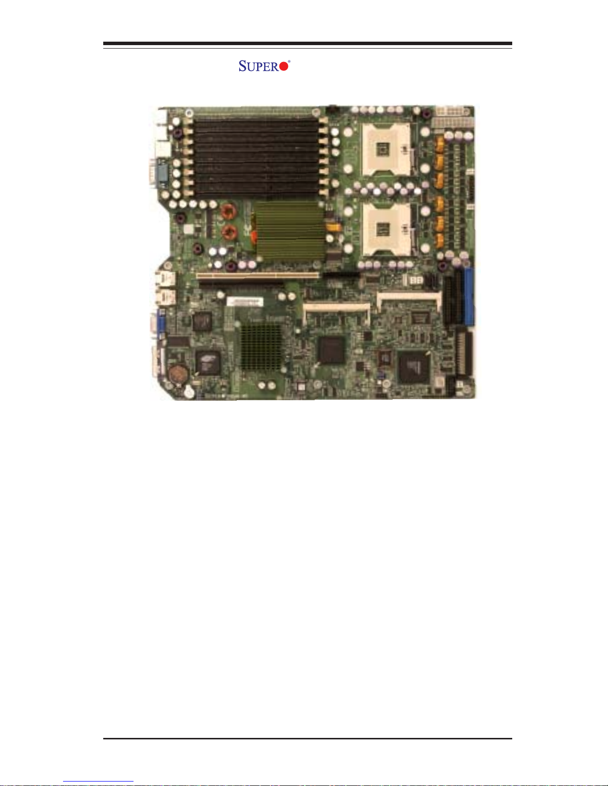
Figure 1-1. X6DAR-8G/X6DAR-iG Image
Page 10

1-4
Introduction
X6DAR-8G/X6DAR-iG User's Manual
Figure 1-2. SUPER X6DAR-8G/X6DAR-iG Motherboard Layout
1. Jumpers not indicated are for test purposes only.
(not drawn to scale)
KB
DIMM 4B
Mouse
USB
0/1
J14
COM1
DIMM 4A
DIMM 3B
DIMM 3A
DIMM 2B
DIMM 2A
DIMM 1B
DIMM 1A
GLAN1
GLAN2
VGA
SCSI Ch B
Battery
JPG1(VGA Enable)
JPL1(LAN Enable)
RAGEX
GLAN
CTRL
PXH
VGA
CTRL
PCI-E x16
PCI-X 133MHz
E7525
(Tumwater)
North Bridge
ICH5R
(South
Bridge)
ZCR
IPMI 2.0
BIOS
S I/O
7902
SCSI
CTRL
IDE #1
IDE #2
Floppy
SCSI Ch A
WOL
COM2
SCSI
Enable
USB2/3
JD2
JP9
CLR CMOS
Force PW-On
WOR
SPK
SW
SCSI
Ter. A
JPA1
JBT1
SMB
FAN5
SATA1
SATA0
FP CTRL
JF1
FAN2
FAN1
20-PinPW
8-Pin
CPU
4-Pin
PW
PW SMB
PW
LED
Chas
Intru.
JL1
JWD
WD
CPU1
CPU2
JPA3
JPA2
SCSI Ter. B
OH
J33
J34
J16
J7
J14
JD1
JA1
J5
J6
J12
FAN4
J1B1
J1D1
J38
J32
J4F4
J4F5
Memory
Speed
(*Note:4)
Notes:
2. " " indcates Pin 1.
3. The only difference between the X6DAR-8G and the X6DAR-iG is that
the X6DAR-8G has SCSI.
4. Manufacturer Setting: Do not change the CPU FSB or memory size.
J11
PW
Fail
SPKR
PCI-Ex4
JOH1
JWOR
JPF
JS1
JS2
JP10
3RDPWDetect
Alarm
Reset
JP11
FAN3
Page 11

Chapter 1: Introduction
1-5
Introduction
Jumper Description Default Setting
JBT1 CMOS Clear See Chapter 2
J4F4/J4F5 Memory Size Select See Chapter 2
JPL1 GLAN Enable/Disable Pins 1-2 (Enabled)
JP10 3rd PWR Supply Fail Detect Open (Disabled)
JPA1 SCSI Enable/Disable(*Note) Pins 1-2 (Enabled)
JPA2,JPA3 SCSI Term. A/B Enable (*Note) Open (Enabled)
JPG1 VGA Enable/Disable Pins 1-2 (Enabled)
JWD Watch Dog Pins 1-2 (Reset)
Connector Description
ATX PWR (J1B1) Primary ATX 20-Pin Power Connector
12-V PWR (J38) 4-Pin Power Connector (Required)
CPU PWR (J1D1) 8-Pin CPU Power Connector( Required)
COM(J14)/COM2(J15) COM1/COM2 Serial Port Connectors
FAN#1-5 Onboard CPU Fan/Chassis Fan Headers
DIMM#1A-DIMM#4B Memory (RAM) Slots
Floppy Drive(J12) Floppy Drive Connector
GLAN1/2 G-bit Ethernet Ports
IPMI (J9) IPMI 2.0 Connector
IDE1/2(J5/J6) IDE1/2 Hard Disk Drive Connectors
KB/Mouse(J33, J34) PS/2 Keyboard (J34)/Mouse (J33)
PWR Fail (JP9) Triple Redundant PS Fail Detect Header
Power SMB(J32) Power System Mangement Bus (See Chapter 2)
SCSI Ch.A/B(JA1/JA2) SCSI Ch. A (JA2), SCSI Ch. B (JA1) Headers
SMB(J11) System Management Bus Header
JD1 PWR LED(Pins1-3), Speaker(Pins4-7) Header
JF1 Front Control Panel Connector
JL1 Chassis Intrusion Header
JP11 Alarm Rest Header (Defult: On)
JOH1 Overheat LED
JWOL Wake-on-LAN Header
JWOR Wake-on-Ring Header
SATA0(J3)/SATA1(J4) Serial ATA Connectors
Video(LG5) Video Connector
USB0/1(J16) Universal Serial Bus Ports
USB2/3(JD2) Front Panel USB0/1 Headers
(*Note: for X6DAR-8G only)
Quick Reference (X6DAR-8G/X6DAR-iG)
(*Please refer to Chapter 2 for pin definitions and detailed
information.)
Page 12

1-6
Introduction
X6DAR-8G/X6DAR-iG User's Manual
Motherboard Features
CPU
• Single or dual Intel® 604-pin Xeon 32-bit/w. EM64T NoconaTM proces-
sors at a 800 MHz front side (system) bus speed.
*Notes: The CPU FSB is set at 800 MHz by the Manufacturer. Please do
not change the CPU FSB setting. Please refer to the support section of
our web site for a complete listing of supported processors.
Memory
• Eight 72-bit, 184-pin gold-plated DIMM sockets supporting up to 16 GB
DDR-333 (PC 2700) or 32 GB DDR-266 (PC 2100) Registered ECC
Memory SDRAM (*Manufacturer Setting)
Notes: Memory is set via BIOS. Interleaved memory; requires memory
modules to be installed in pairs. See Section 2-3 for details.
Chipset
• Intel E7525 (Tumwater) chipset
Expansion Slots
• X6DAR-8G/X6DAR-iG
One x16 PCI-Express slot,
One x4 PCI-Express slot, or
One 64-bit 133 MHz PCI-X (3.3V) slot
BIOS
• 8 Mb Phoenix® Flash ROM
• APM 1.2, DMI 2.1, PCI 2.2, ACPI 1.0, Plug and Play (PnP), SMBIOS 2.3
PC Health Monitoring
• Onboard voltage monitors for CPU cores, chipset voltage, memory
voltage, +3.3V, +5V, +12V, −12V and 5V standby
• Fan status monitor with firmware/software on/off control
• CPU/chassis temperature monitors
• Environmental temperature monitor and control
• CPU fan auto-off in sleep mode
• CPU slow-down on temperature overheat
• CPU thermal trip support for processor protection, +5V standby alert
LED
• Power-up mode control for recovery from AC power loss
Page 13

Chapter 1: Introduction
1-7
Introduction
• Auto-switching voltage regulator for CPU core
• System overheat LED and control
• Chassis intrusion detection
• System resource alert (via Supero Doctor III)
ACPI Features (optional)
• Microsoft OnNow
• Slow blinking LED for suspend state indicator
• Main switch override mechanism
Onboard I/O
• Adaptec 7902 Controller supporting Dual-Channel Ultra 320 SCSI with
RAID0, RAID1, RAID10, JBOD support (*X6DAR-8G only)
• Support for Zero-Channel RAID with Adaptec 2015S ZCR Card (*Card
not included) (*See note below.)
• One IPMI 2.0 socket
• One Intel 82546GB Dual-Port Gigabit Ethernet Controller with support
for 10BASE-T, 100BASE-TX, and 1000BASE-T, RJ45 output
• Dual EIDE channels support up to four Ultra DMA IDE devices
• 1 floppy port interface (up to 2.88 MB)
• 2 Fast UART 16550A compatible serial ports
• PS/2 mouse and PS/2 keyboard ports
• Up to 4 USB 2.0 compliant/1.1 compliant (Universal Serial Bus) ports
• Two Serial ATA via ICH5R SATA controller
Other
• Internal/external modem ring-on
• Wake-on-LAN (WOL)
• Wake-on-Ring (WOR)
• Console redirection
CD/Diskette Utilities
• BIOS flash upgrade utility and device drivers
Dimensions
• ATX Ext. 12" x 13.05" (304.8 x 331.5 mm)
(*Note: If ZCR 2015S is used, please change the SCSI Bus to PCI 66MHz
in the BIOS.)
Page 14
1-8
Introduction
X6DAR-8G/X6DAR-iG User's Manual
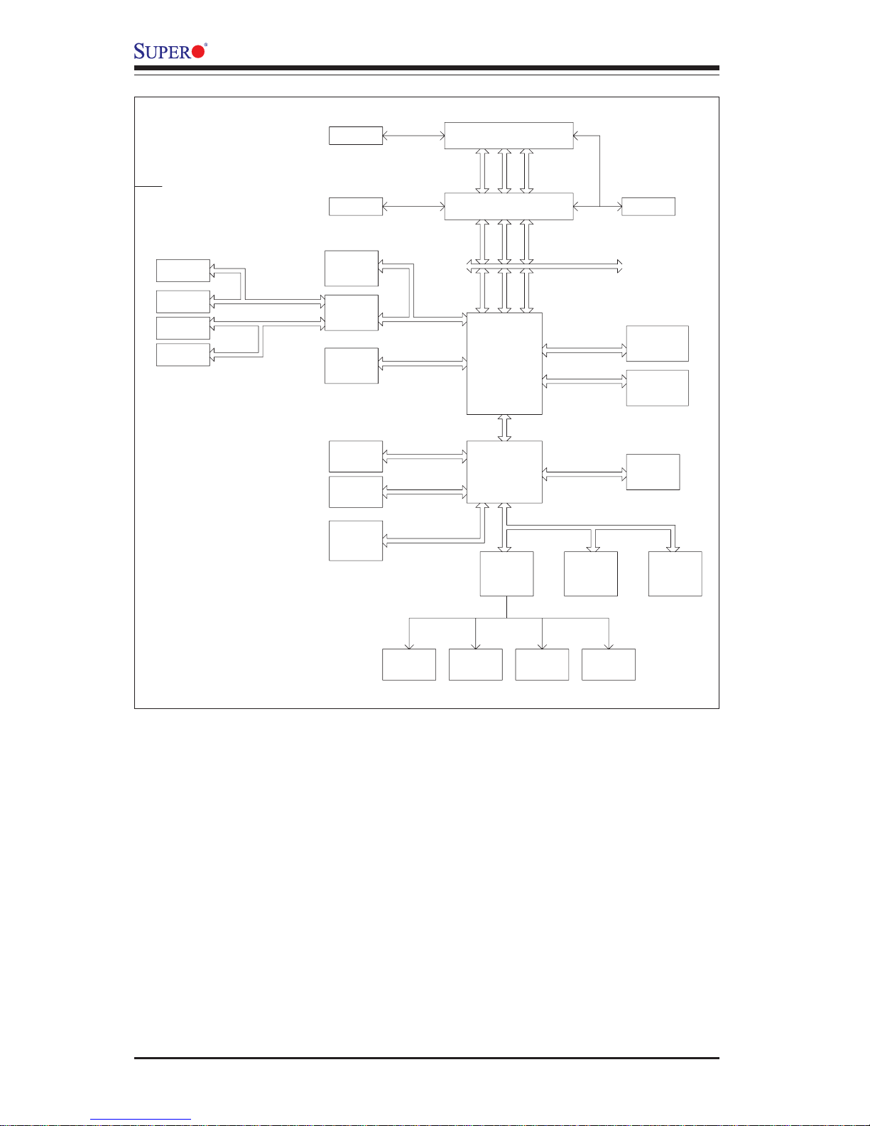
Figure 1-9. Block Diagram of the E7525 Chipset
Note: This is a general block diagram. Please refer to the Motherboard
Features for details.
MCH
NOCONA PROCESSOR#2VRM
CLOCK
4 DDR-266
ADDR
CTRL
DATA
NOCONA PROCESSOR#1
ADDR
CTRL
DATA
DATA
ADDR
CTRL
DIMMs
ICH5R
FWHLPC I/O
LPC BUS
HUB
BMC CON.
DDRA-266
DDRB-266
PCI BUS(32-BIT)
DIMMs
4 DDR-333
USB
0,1,2,3
USB PORT
VGA
KB.
SER.2
SER.1
H/W
MONITOR
FDD.
MS.
VRM
0, 1
SATA
SATA
UDMA-100
IDE
PRI/SEC
A
PXH
B
PCI EXP. A(X8)
SCSI
7902
PCI-X BUS(100 MHZ)
Gbit LAN
ANVIK
SOCKET
ZCR
PCI EXP. (X16)
PCI-X BUS(100 MHZ)
SLOT
1_PCI-X133
266MB/s
4GB/s
6.4GB/s
DDR-333
PCI EXP. A(X4)
PCI EXP. A(X4)
PCI-E_(X4)
PCI-E_(X16)
Page 15

Chapter 1: Introduction
1-9
Introduction
1-2 Chipset Overview
Built upon the functionality and the capability of the E7525 Tumwater
chipset, the X6DAR-8G/X6DAR-iG motherboard provides the performance
and feature set required for dual processor-based computer systems, with
configuration options optimized for communications, presentation, storage,
computation or database applications. The Intel E7525 Tumwater chipset
consists of the following components: the E7525 Tumwater Memory Controller Hub (MCH), the I/O Controller Hub (ICH5R), and the PCI-X Hub (PXH).
The E7525 Tumwater MCH supports single or dual Nocona processors with
Front Side Bus speeds of up to 800 MHz(*Note). Its memory controller provides direct connection to two channels of registered DDR333/DDR266 with
a marched system bus address and data bandwidths of up to 2.7 GB/s
(DDR 333) per channel. The E7525 Tumwater also supports the new PCI
Express high speed serial I/O interface for superior I/O bandwidth. The MCH
provides configurable x16 PCI Express interfaces which may alternatively
be configured as two independent x8 PCI Express interfaces. These interfaces support connection of the MCH to a variety of other bridges that are
compliant with the PCI Express Interface Specification, Rev. 1.0a. The MCH
interfaces with the ICH5R ICH I/O Controller Hub via HI 1.5 Hub Interface.
The PXH can be configured to support for 32- or 64-bit PCI devices running
at 33 MHz, 66 MHz, 100 MHz, and 133 MHz.
ICH5R System Features
In addition to providing the I/O subsystem with access to the rest of the
system, the ICH5R I/O Controller Hub integrates many I/O functions.
The ICH5R I/O Controller Hub integrates: 2-channel Ultra ATA/100 Bus Master IDE Controller, two Serial ATA (SATA) Host w/RAID0, RAID1 support,
SMBus 2.0 Controller, LPC/Flash BIOS Interface, PCI 2.3 Interface and
System Management Controller.
(*Notes: The CPU FSB speed is set at 800 MHz by the Manufacturer.
Please do not change the CPU FSB setting.)
Page 16

1-10
Introduction
X6DAR-8G/X6DAR-iG User's Manual
1-3 Special Features
Recovery from AC Power Loss
BIOS provides a setting for you to determine how the system will respond
when AC power is lost and then restored to the system. You can choose
for the system to remain powered off (in which case you must hit the
power switch to turn it back on) or for it to automatically return to a poweron state. See the Power Lost Control setting in the Advanced BIOS Setup
section (Peripheral Device Configuration) to change this setting. The default setting is Always On.
1-4 PC Health Monitoring
This section describes the PC health monitoring features of the SUPER
X6DAR-8G/X6DAR-iG. All have an onboard System Hardware Monitor chip
that supports PC health monitoring.
Onboard Voltage Monitors for the CPU Cores, Chipset
Voltage, Memory Voltage +3.3V, +5V, +12V, -12V and +5V
Standby
An onboard voltage monitor will scan these voltages continuously. Once a
voltage becomes unstable, a warning is given or an error message is sent
to the screen. Users can adjust the voltage thresholds to define the
sensitivity of the voltage monitor.
Fan Status Monitor with Firmware/Software On/Off Control
The PC health monitor can check the RPM status of the cooling fans. The
onboard CPU and chassis fans are controlled by the Thermal Management
via BIOS.
Environmental Temperature Control
The thermal control sensor monitors the CPU temperature in real time and
will turn on the thermal control fan whenever the CPU temperature exceeds
a user-defined threshold. The overheat circuitry runs independently from
the CPU. It can continue to monitor for overheat conditions even when the
CPU is in sleep mode. Once it detects that the CPU temperature is too high,
it will automatically turn on the thermal control fan to prevent any overheat
Page 17

Chapter 1: Introduction
1-11
Introduction
damage to the CPU. The onboard chassis thermal circuitry can monitor the
overall system temperature and alert users when the chassis temperature
is too high.
CPU Fan Auto-Off in Sleep Mode
The CPU fan activates when the power is turned on. It continues to operate
when the system enters Standby mode. When in sleep mode, the CPU will
not run at full power, thereby generating less heat.
Overheat/Fan Fail LED and Control
This feature is available when the user enables the Overheat/Fan Fail
warning function in the BIOS. This allows the user to define an overheat
temperature. When this temperature is exceeded, both the overheat fan and
the warning LED are triggered.
System Resource Alert (*via Supero Doctor III)
This feature is available when used with Intel's LANDesk Client Manager
(optional). For example, if the system is running low on virtual memory and
there is insufficient hard drive space for saving the data, you can be
alerted of the potential problem.
Auto-Switching Voltage Regulator for the CPU Core
The auto-switching voltage regulator for the CPU core can support autosense voltage IDs ranging from 0.8375V to 1.6V. This will allow the regulator to run cooler and thus make the system more stable.
1-5 ACPI Features
ACPI stands for Advanced Configuration and Power Interface. The ACPI
specification defines a flexible and abstract hardware interface that provides a standard way to integrate power management features throughout
a PC system, including its hardware, operating system and application software. This enables the system to automatically turn on and off peripherals
such as CD-ROMs, network cards, hard disk drives and printers. This also
includes consumer devices connected to the PC such as VCRs, TVs, telephones and stereos.
Page 18

1-12
Introduction
X6DAR-8G/X6DAR-iG User's Manual
In addition to enabling operating system-directed power management, ACPI
provides a generic system event mechanism for Plug and Play and an operating system-independent interface for configuration control. ACPI leverages the Plug and Play BIOS data structures while providing a processor
architecture-independent implementation that is compatible with Windows
Operating Systems.
Microsoft OnNow
The OnNow design initiative is a comprehensive, system-wide approach to
system and device power control. OnNow is a term for a PC that is always
on but appears to be off and responds immediately to user or other requests.
Slow Blinking LED for Suspend-State Indicator
When the CPU goes into a suspend state, the chassis power LED will start
blinking to indicate that the CPU is in suspend mode. When the user presses
any key, the CPU will wake-up and the LED will automatically stop blinking
and remain on.
Main Switch Override Mechanism
When an ATX power supply is used, the power button can function as a
system suspend button to make the system enter a SoftOff state. The
monitor will be suspended and the hard drive will spin down. Depressing
the power button again will cause the whole system to wake-up. During
the SoftOff state, the ATX power supply provides power to keep the required circuitry in the system alive. In case the system malfunctions and
you want to turn off the power, just depress and hold the power button for
4 seconds. This option can be set in the Power section of the BIOS Setup
routine.
External Modem Ring-On
Wake-up events can be triggered by a device such as the external modem
ringing when the system is in the SoftOff state. Note that external modem
ring-on can only be used with an ATX 2.01 (or above) compliant power
supply.
Page 19

Chapter 1: Introduction
1-13
Introduction
Wake-On-LAN (WOL)
Wake-On-LAN is defined as the ability of a management application to remotely power up a computer that is powered off. Remote PC setup, updates and asset tracking can occur after hours and on weekends so that
daily LAN traffic is kept to a minimum and users are not interrupted. The
motherboard has a 3-pin header (WOL) to connect to the 3-pin header on a
Network Interface Card (NIC) that has WOL capability. Wake-On-LAN must
be enabled in BIOS. Note that Wake-On-LAN can only be used with an ATX
2.01 (or above) compliant power supply.
1-6 Power Supply
As with all computer products, a stable power source is necessary for
proper and reliable operation. It is even more important for processors that
have high CPU clock rates.
The SUPER X6DAR-8G/X6DAR-iG accommodates ATX power 20-pin supplies. Although most power supplies generally meet the specifications required by the system, some are inadequate. You should use one that will
supply at least 400W of power.
It is strongly recommended that you use a high quality power supply that
meets ATX power supply Specification 2.02 or above. It must also be SSI
compliant (info at http://www.ssiforum.org/). Additionally, in areas where
noisy power transmission is present, you may choose to install a line filter
to shield the computer from noise. It is recommended that you also install a
power surge protector to help avoid problems caused by power surges.
(*Please refer to the next page for additional information.)
NOTES: 1. A 12V 8-pin power (JID1) is required to support Intel
Nocona CPUs. In addition, a 12V 4-pin PWR connection is also required for the system to function properly. See Section 2-5 for
details on connecting the power supply cables.
2. Be sure to use the correct type of onboard CMOS battery as
specified by the Manufacturer. Do not install the CMOS battery upside down to avoid possible explosion.
Page 20

1-14
Introduction
X6DAR-8G/X6DAR-iG User's Manual
1-7 Super I/O
The disk drive adapter functions of the Super I/O chip include a floppy disk
drive controller that is compatible with industry standard 82077/765, a data
separator, write pre-compensation circuitry, decode logic, data rate selection, a clock generator, drive interface control logic and interrupt and DMA
logic. The wide range of functions integrated onto the Super I/O greatly
reduces the number of components required for interfacing with floppy disk
drives. The Super I/O supports 360 K, 720 K, 1.2 M, 1.44 M or 2.88 M disk
drives and data transfer rates of 250 Kb/s, 500 Kb/s or 1 Mb/s. It also
provides two high-speed, 16550 compatible serial communication ports
(UARTs), one of which supports serial infrared communication. Each UART
includes a 16-byte send/receive FIFO, a programmable baud rate generator,
complete modem control capability and a processor interrupt system. Both
UARTs provide legacy speed with baud rate of up to 115.2 Kbps as well as
an advanced speed with baud rates of 250 K, 500 K, or 1 Mb/s, which
support higher speed modems.
The Super I/O supports one PC-compatible printer port (SPP), Bi-directional
Printer Port (BPP) , Enhanced Parallel Port (EPP) or Extended Capabilities
Port (ECP).
The Super I/O provides functions that comply with ACPI (Advanced Configuration and Power Interface), which includes support of legacy and ACPI
power management through an SMI or SCI function pin. It also features
auto power management to reduce power consumption.
The IRQs, DMAs and I/O space resources of the Super I/O can flexibly
adjust to meet ISA PnP requirements, which support ACPI and APM (Advanced Power Management).
Page 21

Chapter 2: Installation
2-1
Chapter 2
Installation
2-1 Static-Sensitive Devices
Electric-Static-Discharge (ESD) can damage electronic components. To prevent damage to your system board, it is important to handle it very carefully.
The following measures are generally sufficient to protect your equipment
from ESD.
Precautions
• Use a grounded wrist strap designed to prevent static discharge.
• Touch a grounded metal object before removing the board from the antistatic bag.
• Handle the board by its edges only; do not touch its components, peripheral chips, memory modules or gold contacts.
• When handling chips or modules, avoid touching their pins.
• Put the motherboard and peripherals back into their antistatic bags when
not in use.
• For grounding purposes, make sure your computer chassis provides excellent conductivity between the power supply, the case, the mounting
fasteners and the motherboard.
Warning: Please use the correct type of onboard CMOS battery as
specified by the Manufacturer. Do not install the CMOS battery upside down to avoid possible explosion.
Unpacking
The motherboard is shipped in antistatic packaging to avoid static damage.
When unpacking the board, make sure the person handling it is static protected.
Page 22
2-2
X6DAR-8G/X6DAR-iG User's Manual
IMPORTANT: Always connect the power cord last and always remove it
before adding, removing or changing any hardware components. Make
sure that you install the processor into the CPU socket before you install
the CPU heat sink.
2-2 Nocona Processor and Heatsink Installation
When handling the processor package, avoid placing direct
pressure on the label area of the fan. Also, do not place the
motherboard on a conductive surface, which can damage the
BIOS battery and prevent the system from booting up.
!
Socket lever
CPU Installation
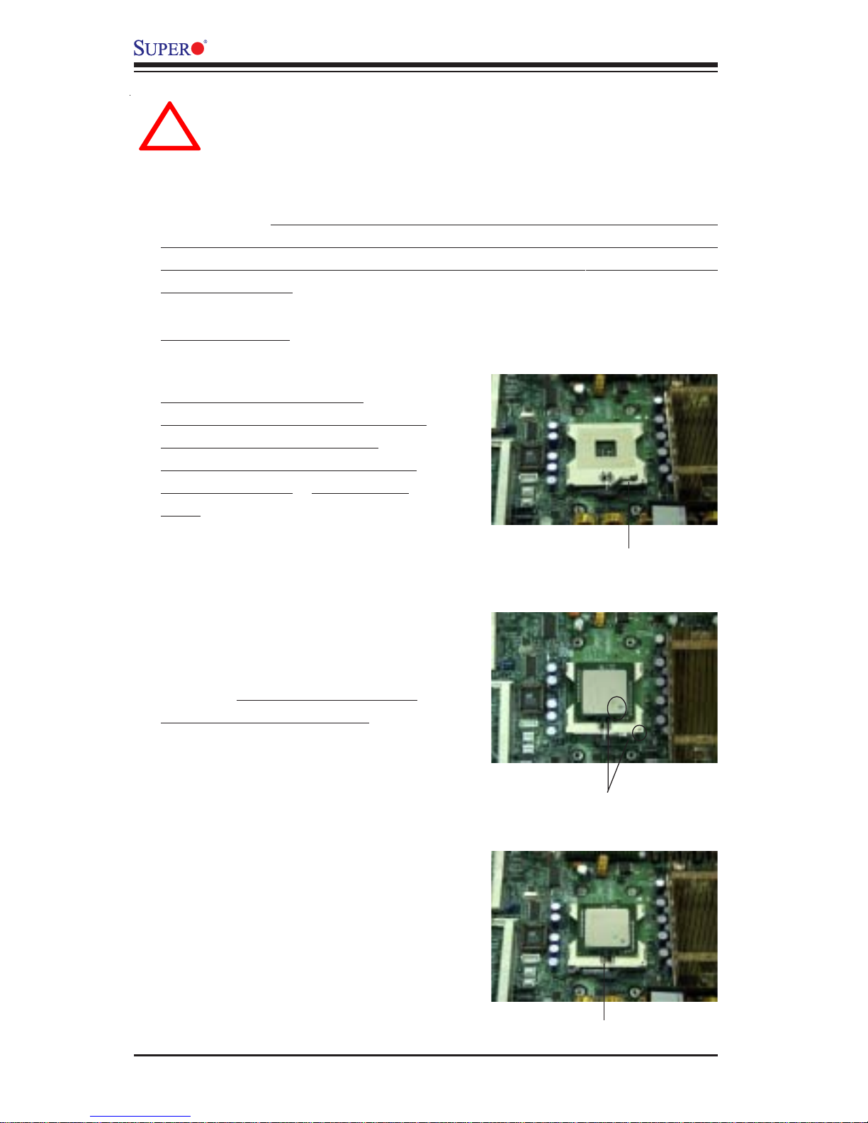
1. Lift the lever on the CPU socket:
lift the lever to the upright
position as shown in the picture on
the right; otherwise, you will
damage the CPU socket when you
turn on the power. (Install CPU1
first.)
Pin 1
2. Insert the CPU in the socket and
make sure that pin 1 of the CPU
aligns with pin 1 of the socket
(both corners are marked with a
triangle). If only one CPU is used,
install it into CPU socket #1
(socket #2 is automatically disabled
if only one CPU is used).
3. Press the lever down until
you hear the *click* to make
sure that the CPU is securely
installed in the CPU socket.
Socket lever
Page 23
Chapter 2: Installation
2-3
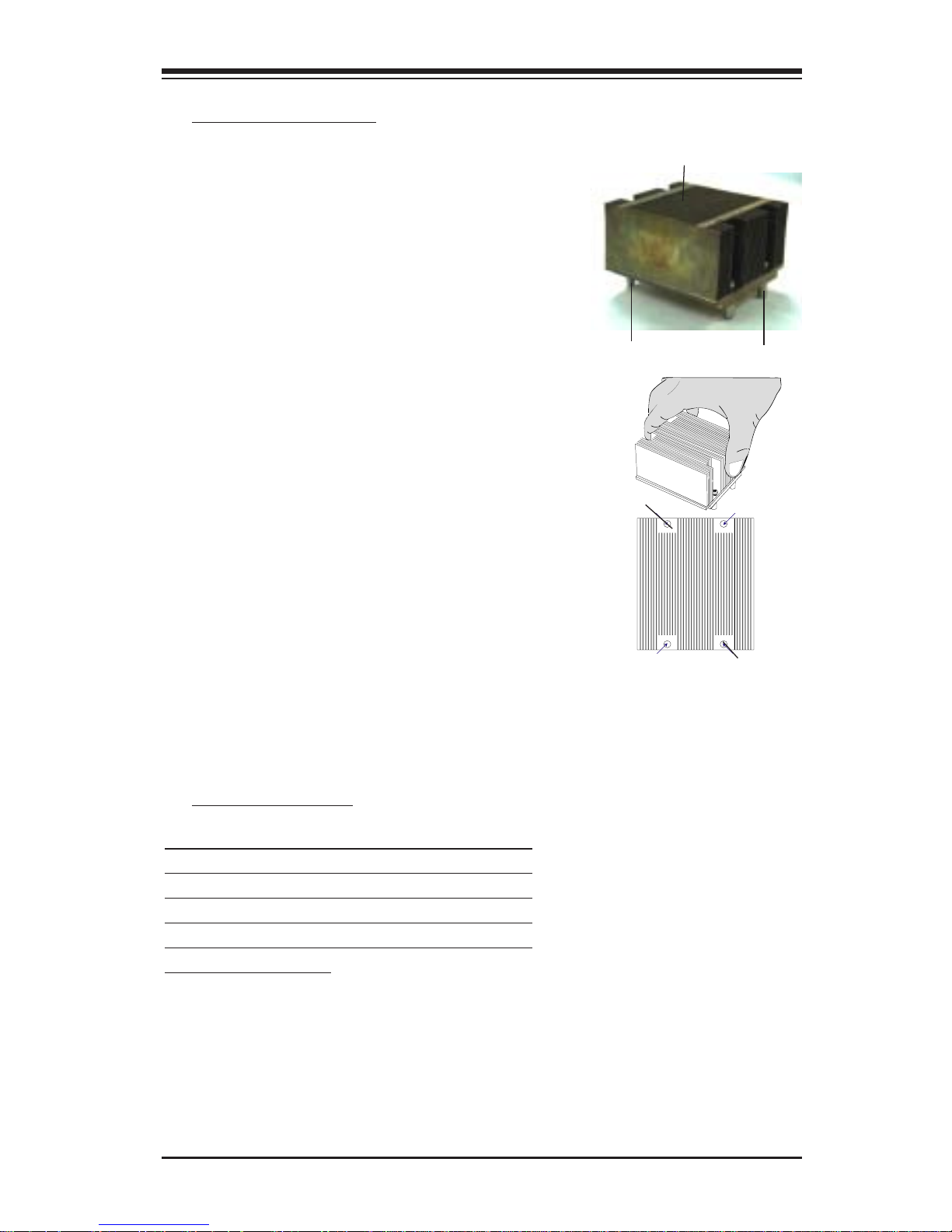
Heatsink
Heatsink Installation
1. Do not apply any thermal compound
to the heatsink or the CPU die-the
required amount has already been
applied.
2. Place the heatsink on top of the
CPU so that the four mounting holes
are aligned with those on the retention
mechanism.
3. Screw in two diagonal screws (ie
the #1 and the #2 screws) until just
snug (-do not fully tighten the screws
to avoid possible damage to the CPU.)
4. Finish the installation by fully
tightening all four screws.
Screw#1
Screw#2
Screw#1
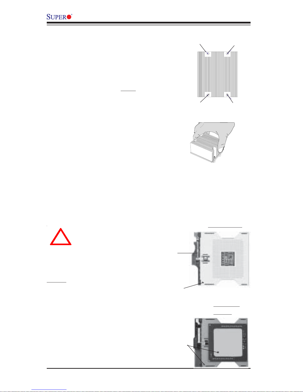
Heatsink Removal
(Caution! We do not recommend that the CPU
or the heatsink be removed. However, if you
do need to un-install the heatsink, please follow the instructions below to remove the
heatsink to prevent damage done to the CPU
or the CPU socket. )
Page 24
2-4
X6DAR-8G/X6DAR-iG User's Manual
Figure 2-1. PGA604 Socket: Empty and with Processor Installed
Lever
Processor
(installed)
Triangle
Triangle
Empty socket
Warning! Make
sure to lift the lever
upward when
installing the CPU. If
the lever is only
raised partially,
damage to the
socket or CPU may
occur.
!
1. Unscrew and remove the heatsink
screws from the motherboard in the
sequence as show in the second
picture on the right.
2. Hold the heatsink as show in the
picture on the right and gently wriggle
the heatsink to loosen it from the CPU.
(Do not use excessive force when
wriggling the heatsink!!)
3. Once the CPU is loosened from the
heatsink, remove the heatsink from the
CPU socket.
4. Clean the surface of the CPU and
the heatsink to get rid of the old
thermal grease. Reapply the proper
amount of thermal grease on the
surface before you re-install the CPU
and the heatsink.
Screw#1
Screw#2
Screw#3
Screw#4
Page 25

Chapter 2: Installation
2-5
Mounting the Motherboard in the Chassis
All motherboards have standard mounting holes to fit different types of
chassis. Make sure that the locations of all the mounting holes for both the
motherboard and the chassis match. Although a chassis may have both
plastic and metal mounting fasteners, metal ones are highly recommended
due to the fact that they ground the motherboard to the chassis. Make
sure that the metal standoffs click in or are screwed in tightly. Then use a
screwdriver to secure the motherboard on the motherboard tray.
Page 26
2-6
X6DAR-8G/X6DAR-iG User's Manual
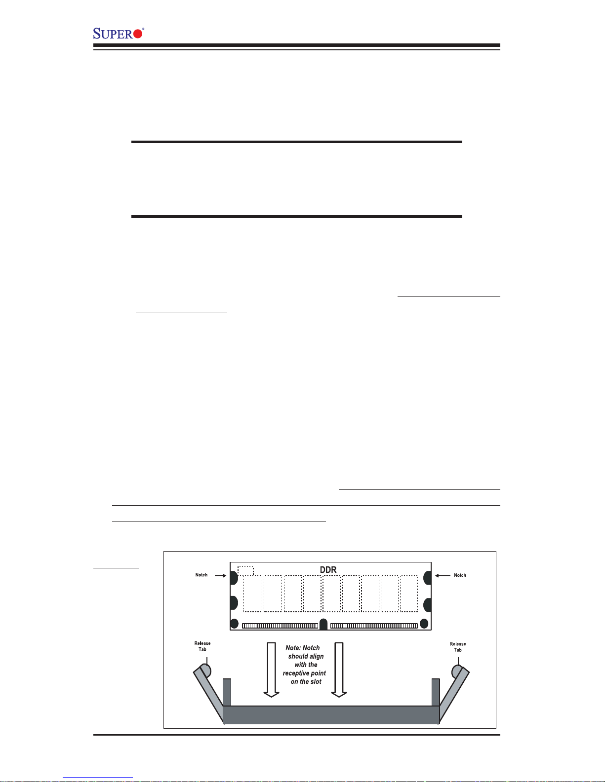
Figure 2-2. Installing and Removing DIMMs
To Install:
Insert the
module
vertically and
press down
until it snaps
into place.
Pay attention
to the
alignment
notch at the
bottom.
2-3 Installing DIMMs
Note: Check the Supermicro web site for recommended memory modules:
http://www.supermicro.com/TECHSUPPORT/FAQs/Memory_vendors.htm
CAUTION
Exercise extreme care when installing or removing DIMM
modules to prevent any possible damage. Also note that the
memory is interleaved to improve performance (see step 1).
DIMM Installation (See Figure 2-2)
1. Insert the desired number of DIMMs into the memory slots, starting with
DIMM 1A. The memory scheme is interleaved so you must install two
modules at a time, beginning with DIMM 1A, then DIMM 1B, and so on.
2. Insert each DIMM module vertically into its slot. Pay attention to the
notch along the bottom of the module to prevent inserting the DIMM
module incorrectly.
3. Gently press down on the DIMM module until it snaps into place in the
slot. Repeat for all modules (see step 1 above).
Memory Support
The X6DAR-8G/X6DAR-iG supports up to 32/16 GB of Registered DDR-266/
333(PC2100/2700) memory (recommended by the Manufacturer). All
motherboards were designed to support 2 GB modules in each slot, but has
only been verified for up to 1.0 GB modules. If Reg. ECC DDR 333 (PC2700)
memory modules are used, 4 pieces of double banked memory and 6 pieces
of single banked memory are supported.
Page 27
Chapter 2: Installation
2-7
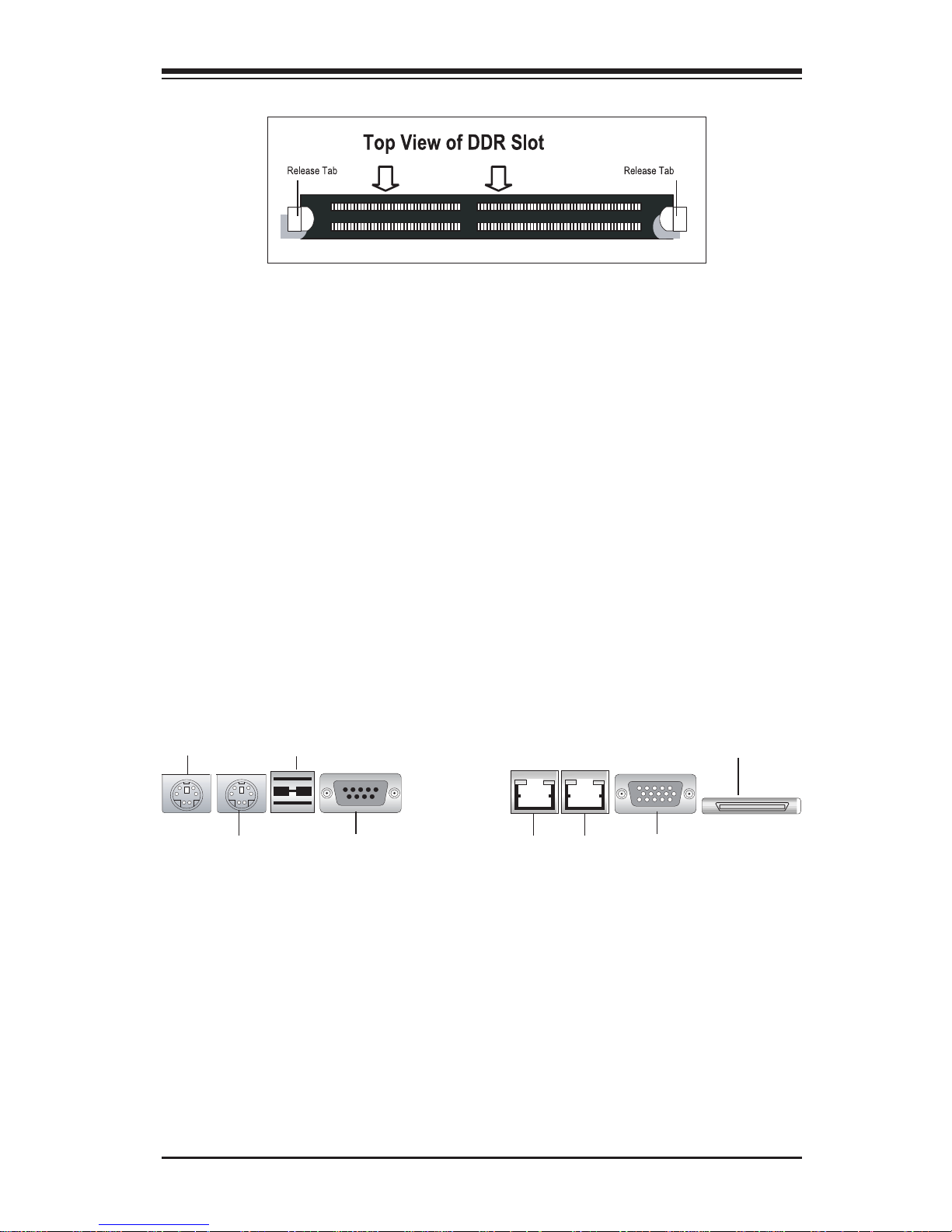
To Remove:
Use your thumbs to gently push near the edge of both ends of
the module. This should release it from the slot.
2-4 I/OPorts/Control Panel Connectors
The I/O ports are color coded in conformance with the PC 99 specification.
See Figure 2-3 below for the colors and locations of the various I/O ports.
Figure 2-3. I/O Port Locations and Definitions
Mouse (Purple)
Keyboard
(Turquoise)
GLAN1
COM Port1
GLAN2
USB0/1
Video
SCSI(X6DAR-8G
only)
Page 28
2-8
X6DAR-8G/X6DAR-iG User's Manual
Front Control Panel
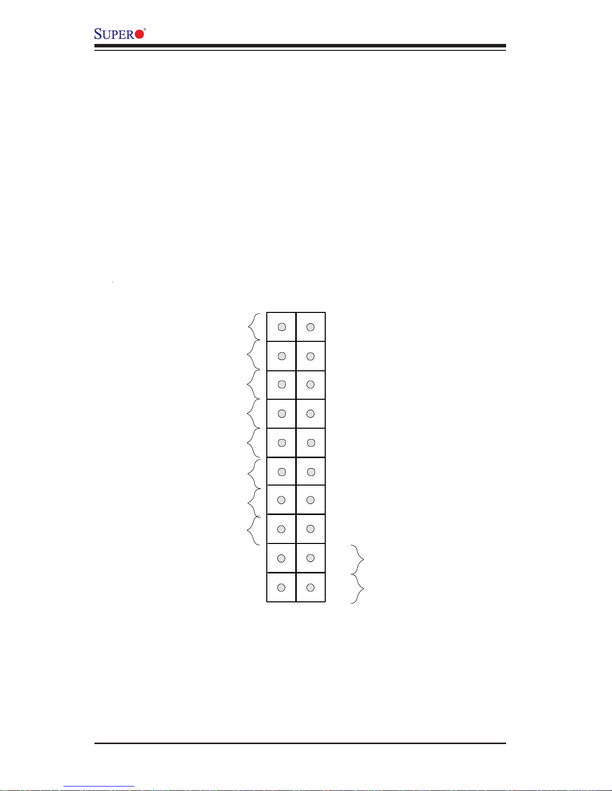
JF1 contains header pins for various buttons and indicators that are normally located on a control panel at the front of the chassis. These connectors are designed specifically for use with Supermicro server chassis. See
Figure 2-4 for the descriptions of the various control panel buttons and LED
indicators. Refer to the following section for descriptions and pin definitions.
Figure 2-4. JF1 Header Pins
Power Button
Overheat/Fan Fail LED
1
NIC1 LED
Reset Button
2
Power Fail LED
HDD LE D
Power LED
Reset
Pwr
Vcc
Vcc
Vcc
Vcc
Ground
Ground
1920
Vcc
X
Ground
NMI
X
NIC2 LED
Vcc
Page 29
Chapter 2: Installation
2-9
JP9
FAN1
20-PinPW
8-Pin
CPU
4-Pin
PW
J1B1
J1D1
J38
PW
Fail
JP10
3RD
PW
Detect
Alarm
Reset
JP11
K
B
DIMM 4B
Mouse
USB
0/1
J14
C
O
M
1
DIMM 4A
DIMM 3B
DIMM 3A
DIMM 2B
DIMM 2A
DIMM 1B
DIMM 1A
G
L
A
N
1
G
L
A
N
2
VGA
S
C
S
I C
h
B
B
a
tte
ry
JP
G
1
(V
G
A
E
n
a
b
le
)
JP
L
1
(L
A
N
E
n
a
b
le
)
R
A
G
E
-
X
G
L
A
N
C
T
R
L
P
X
H
V
G
A
C
T
R
L
P
C
I-E
x1
6
P
C
I-X
1
3
3
M
H
z
E
7
5
25
(T
u
m
w
a
te
r)
N
o
rth
B
rid
g
e
IC
H
5
R
(S
o
u
th
B
rid
g
e
)
Z
C
R
IPMI 2.0
BIOS
S I/O
7902
SCSI
CTRL
IDE #1
IDE #2
Floppy
SCSI Ch A
WOL
COM2
SCSI
Enable
USB2/3
JD2
JP9
CLR CMOS
Force PW-On
WOR
SPK
SW
SCSI
Ter. A
JPA1
JBT1
S
M
B
FAN5
S
A
T
A
1
SATA0
F
P
C
T
R
L
JF
1
FAN2
FAN1
20-PinPW
8-Pin
CPU
4-Pin
PW
PW SMB
PW
LED
Chas
Intru.
JL1
JWD
WD
CPU1
CPU2
JPA3
JPA2
S
C
S
I T
e
r. B
OH
J33
J34
J16
J7
J14
JD1
JA1
J5
J6
J12
F
A
N
4
J1B1
J1D1
J38
J32
J4
F
4
J
4
F
5
M
e
m
o
ry
S
p
e
e
d
(*N
o
te
:4
)
J11
PW
Fail
S
P
K
R
P
C
I-E
x4
JOH1
JW
O
R
JPF
JS
1
JS
2
JP
1
0
3RDPWDetect
Alarm
Reset
JP
1
1
F
A
N
3
2-5 Connecting Cables
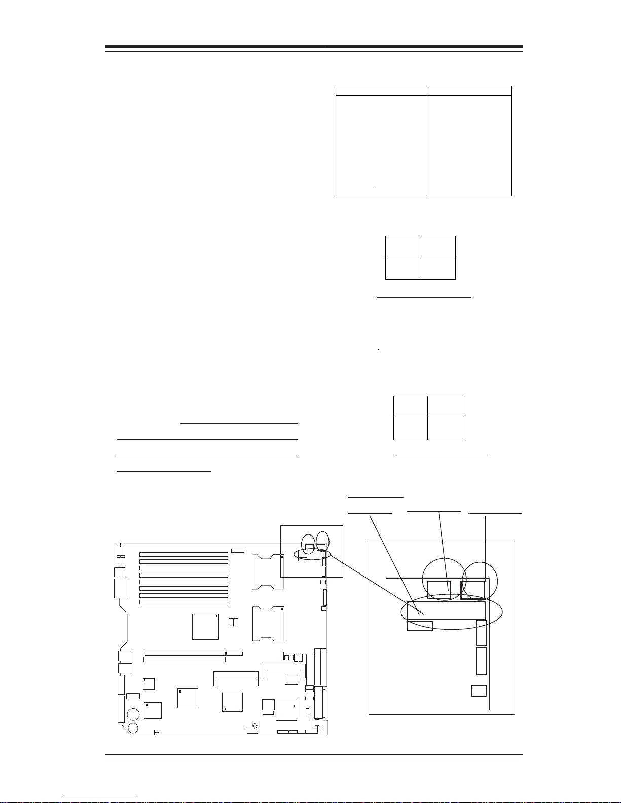
ATX Power Connector
The primary power supply
connector(J1B1) on the X6DAR8G/X6DAR-iG meets the SSI (Superset ATX) 20-pin specification.
You must also connect the 4-pin
(J38) processor power connector
to your power supply. Refer to
the table below right for the J38 4Pin (12V) connector.
Pins
1 thru 4
5 thru 8
Definition
Ground
+12v
8-Pin +12v Power Supply
Connector (J1D1)
Processor Power
Connectors
In addition to the Primary ATX
power connector (above), there is
a 12V 8-pin processor power
connector. The 12V 8-pin connector at J1D1 must also be connected to your power supply for
CPU consumption. See the table
on the right for pin definitions.
Pin # Definition
11 +3.3V
12 -12V
13 COM
14 PS_ON
15 COM
16 COM
17 COM
18 -5V
19 +5V
20 +5V
Pin # Definition
1 +3.3V
2 +3.3V
3COM
4+5V
5COM
6+5V
7COM
8PW-OK
95VSB
10 +12V
ATX 20-pin Power Connector
Pin Definitions (J1B1)
Pins #
1 & 2
3 & 4
Definition
Ground
+12 V
+12V 4-pin
Connector
(J38)
Required Connection
Required Connection
ATX 20Pin PWR
4-Pin PWR
8-Pin PWR
Page 30
2-10
X6DAR-8G/X6DAR-iG User's Manual
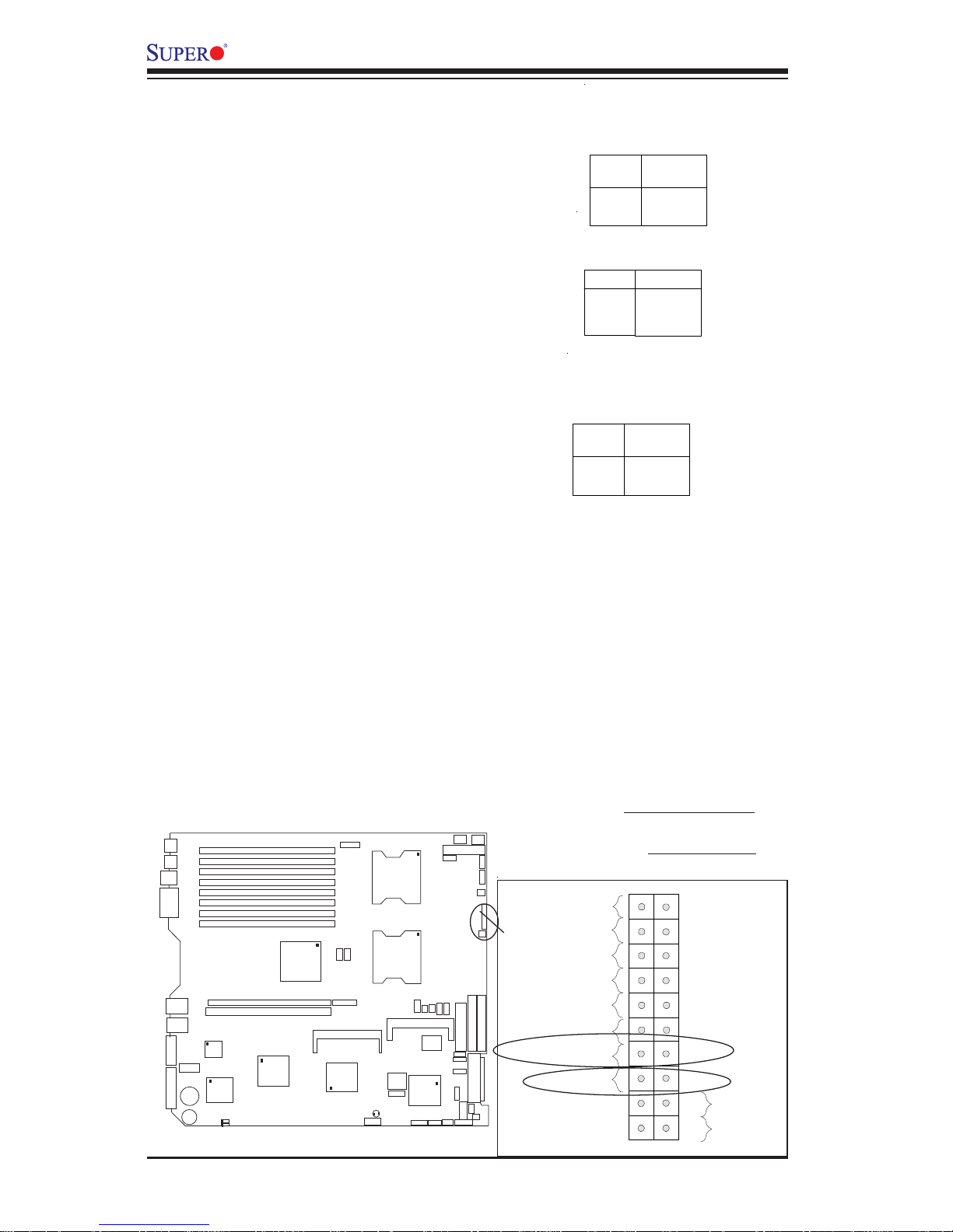
Power LED
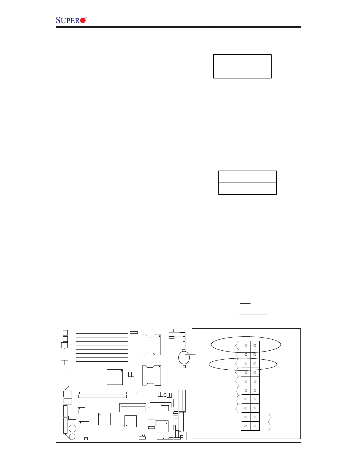
The Power LED connection is located on pins 15 and 16 of JF1.
Refer to the table on the right for
pin definitions.
NMI Button
The non-maskable interrupt button
header is located on pins 19 and
20 of JF1. Refer to the table on
the right for pin definitions.
Pin
Number
19
20
Definition
Control
Ground
NMI Button Pin
Definitions (JF1)
Pin
Number
15
16
Definition
Vcc
Control
PWR_LED Pin Definitions
(JF1)
K
B
DIMM 4B
Mouse
USB
0/1
J14
C
O
M
1
DIMM 4A
DIMM 3B
DIMM 3A
DIMM 2B
DIMM 2A
DIMM 1B
DIMM 1A
G
L
A
N
1
G
L
A
N
2
VGA
S
C
S
I C
h
B
B
a
tte
ry
JP
G
1
(V
G
A
E
n
a
b
le
)
J
P
L
1
(L
A
N
E
na
b
le)
R
A
G
E
-
X
G
L
A
N
C
T
R
L
P
X
H
V
G
A
C
T
R
L
P
C
I-E
x1
6
P
C
I-X
1
3
3
M
H
z
E
7
5
25
(T
u
m
w
a
te
r)
N
o
rth
B
rid
g
e
IC
H
5
R
(S
o
u
th
B
rid
g
e
)
Z
C
R
IPMI 2.0
BIOS
S I/O
7902
SCSI
CTRL
IDE #1
IDE #2
Floppy
SCSI Ch A
WOL
COM2
SCSI
Enable
USB2/3
JD2
JP9
CLR CMOS
Force PW-On
WOR
SPK
SW
SCSI
Ter. A
JPA1
JBT1
S
M
B
FAN5
S
A
T
A
1
SATA0
F
P
C
T
R
L
J
F
1
FAN2
FAN1
20-PinPW
8-Pin
CPU
4-Pin
PW
PW SMB
PW
LED
Chas
Intru.
JL1
JWD
WD
CPU1
CPU2
JPA3
JPA2
S
C
S
I T
e
r. B
OH
J33
J34
J16
J7
J14
JD1
JA1
J5
J6
J12
F
A
N
4
J1B1
J1D1
J38
J32
J4
F
4
J4
F
5
M
e
m
o
ry
S
p
e
e
d
(*N
o
te
:4
)
J11
PW
Fail
S
P
K
R
P
C
I-E
x4
JOH1
JW
O
R
JPF
JS
1
JS
2
JP
1
0
3RDPWDetect
Alarm
Reset
JP
1
1
F
A
N
3
Power Bu tton
Overheat/Fan Fail LED
1
NIC1 LED
Reset Button
2
Power Fail LED
HDD LED
Power LED
Reset
Pwr
Vcc
Vcc
Vcc
Vcc
Ground
Ground
1920
Vcc
X
Ground
NMI
X
NIC2 LED
Vcc
NMI
PWR LED
Page 31
Chapter 2: Installation
2-11
K
B
DIMM 4B
Mouse
USB
0/1
J14
C
O
M
1
DIMM 4A
DIMM 3B
DIMM 3A
DIMM 2B
DIMM 2A
DIMM 1B
DIMM 1A
G
L
A
N
1
G
L
A
N
2
VGA
S
C
S
I C
h
B
B
a
tte
ry
JP
G
1
(V
G
A
E
n
a
b
le
)
JP
L
1
(L
A
N
E
n
a
b
le
)
R
A
G
E
-
X
G
L
A
N
C
T
R
L
P
X
H
V
G
A
C
T
R
L
P
C
I-E
x1
6
P
C
I-X
1
3
3
M
H
z
E
7
5
2
5
(T
u
m
w
ate
r)
N
o
rth
B
rid
g
e
IC
H
5
R
(S
o
u
th
B
rid
g
e
)
Z
C
R
IPMI 2.0
BIOS
S I/O
7902
SCSI
CTRL
IDE #1
IDE #2
Floppy
SCSI Ch A
WOL
COM2
SCSI
Enable
USB2/3
JD2
JP9
CLR CMOS
Force PW-On
WOR
SPK
SW
SCSI
Ter. A
JPA1
JBT1
S
M
B
FAN5
S
A
T
A
1
SATA0
F
P
C
T
R
L
JF
1
FAN2
FAN1
20-PinPW
8-Pin
CPU
4-Pin
PW
PW SMB
PW
LED
Chas
Intru.
JL1
JWD
WD
CPU1
CPU2
JPA3
JPA2
S
C
S
I T
e
r. B
OH
J33
J34
J16
J7
J14
JD1
JA1
J5
J6
J12
F
A
N
4
J1B1
J1D1
J38
J32
J4
F
4
J4
F
5
M
e
m
o
ry
S
p
e
e
d
(*N
o
te
:4
)
J11
PW
Fail
S
P
K
R
P
C
I-E
x4
JOH1
JW
O
R
JPF
JS1
JS
2
JP
1
0
3RDPWDetect
Alarm
Reset
JP
1
1
F
A
N
3
NIC1/NIC2 LED Indicators
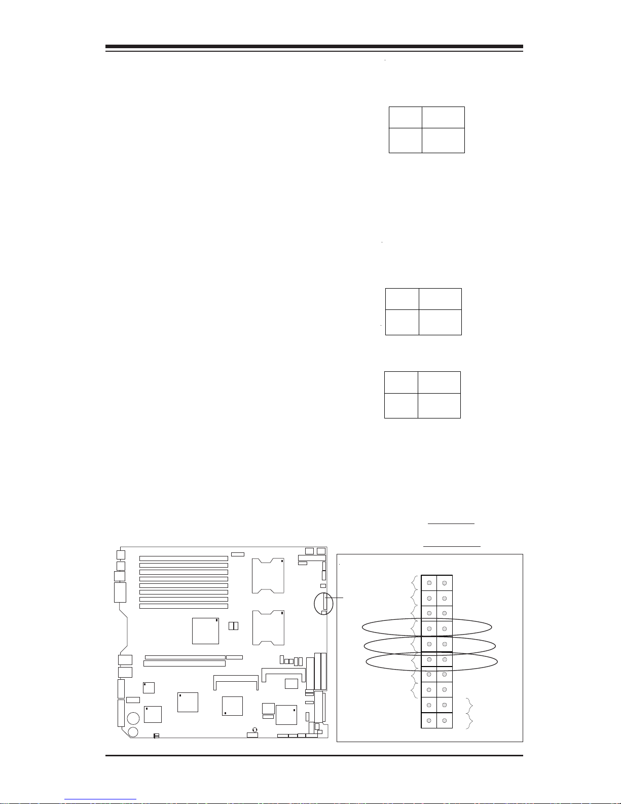
The NIC (Network Interface Controller) LED connection for GLAN
port1 is located on pins 11 and 12
of JF1 and the LED connection for
GLAN Port2 is on Pins 9 and 10.
Attach the NIC LED cables to display network activity. Refer to the
table on the right for pin definitions.
HDD LED
The HDD LED connection is located
on pins 13 and 14 of JF1. Attach
the hard drive LED cable here to
display disk activity (for any hard
drives on the system, including
SCSI, Serial ATA and IDE). See
the table on the right for pin definitions.
HDD LED Pin
Definitions
(JF1)
Pin
Number
13
14
Definition
Vcc
HD Active
NIC1 LED Pin
Definitions
(JF1)
Pin
Number
11
12
Definition
Vcc
GND
NIC2 LED Pin
Definitions
(JF1)
Pin
Number
9
10
Definition
Vcc
GND
Power Bu tton
Overheat/Fan Fail LED
1
NIC1 LED
Reset Button
2
Power Fail LED
HDD LED
Power LED
Reset
Pwr
Vcc
Vcc
Vcc
Vcc
Ground
Ground
1920
Vcc
X
Ground
NMI
X
NIC2 LED
Vcc
NIC1/2 LED
HDD LED
Page 32
2-12
X6DAR-8G/X6DAR-iG User's Manual
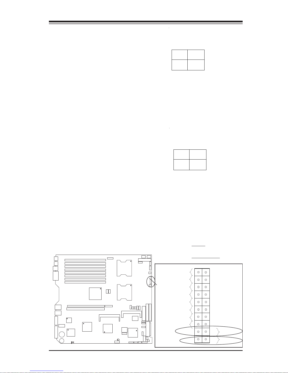
Power Fail LED
The Power Fail LED connection is
located on pins 5 and 6 of JF1.
Refer to the table on the right for
pin definitions.
Power Fail LED Pin
Definitions
(JF1)
Pin
Number
5
6
Definition
Vcc
GND
K
B
DIMM 4B
Mouse
USB
0/1
J14
C
O
M
1
DIMM 4A
DIMM 3B
DIMM 3A
DIMM 2B
DIMM 2A
DIMM 1B
DIMM 1A
G
L
A
N
1
G
L
A
N
2
VGA
S
C
S
I C
h
B
B
a
tte
ry
JP
G
1
(V
G
A
E
n
a
b
le
)
JP
L
1
(L
A
N
E
n
a
b
le
)
R
A
G
E
-
X
G
L
A
N
C
T
R
L
P
X
H
V
G
A
C
T
R
L
P
C
I-E
x1
6
P
C
I-X
1
3
3
M
H
z
E
7
5
2
5
(T
u
m
w
a
te
r)
N
o
rth
B
rid
g
e
IC
H
5
R
(S
o
u
th
B
rid
g
e
)
Z
C
R
IPMI 2.0
BIOS
S I/O
7902
SCSI
CTRL
IDE #1
IDE #2
Floppy
SCSI Ch A
WOL
COM2
SCSI
Enable
USB2/3
JD2
JP9
CLR CMOS
Force PW-On
WOR
SPK
SW
SCSI
Ter. A
JPA1
JBT1
S
M
B
FAN5
S
A
T
A
1
SATA0
F
P
C
T
R
L
JF
1
FAN2
FAN1
20-PinPW
8-Pin
CPU
4-Pin
PW
PW SMB
PW
LED
Chas
Intru.
JL1
JWD
WD
CPU1
CPU2
JPA3
JPA2
S
C
S
I T
e
r. B
OH
J33
J34
J16
J7
J14
JD1
JA1
J5
J6
J12
F
A
N
4
J1B1
J1D1
J38
J32
J4
F
4
J4
F
5
M
e
m
o
ry
S
p
e
e
d
(*N
o
te
:4
)
J11
PW
Fail
S
P
K
R
P
C
I-E
x4
JOH1
JW
O
R
JPF
JS
1
JS
2
JP
1
0
3RDPWDetect
Alarm
Reset
JP
1
1
F
A
N
3
Power Button
Overheat/Fan Fail LED
1
NIC1 LED
Reset Button
2
Power Fail LED
HDD LED
Power LED
Reset
Pwr
Vcc
Vcc
Vcc
Vcc
Ground
Ground
1920
Vcc
X
Ground
NMI
X
NIC2 LED
Vcc
Overheat/FanFail LED
Connect an LED to the OH/Fan Fail
connection on pins 7 and 8 of JF1
to provide advanced warning of
chassis overheating or sytem fan
failure. Refer to the table on the
right for pin definitions.
OH/Fan Fail LED
(JF1)
State
Off
Stay On
Blink
Message
Normal
Overheat
Fan Fail
OH/Fan Fail LED
Pin Definitions
(JF1)
Pin
Number
7
8
Definition
Vcc
GND
OH/Fan Fail LED
PWR Fail LED
Page 33
Chapter 2: Installation
2-13
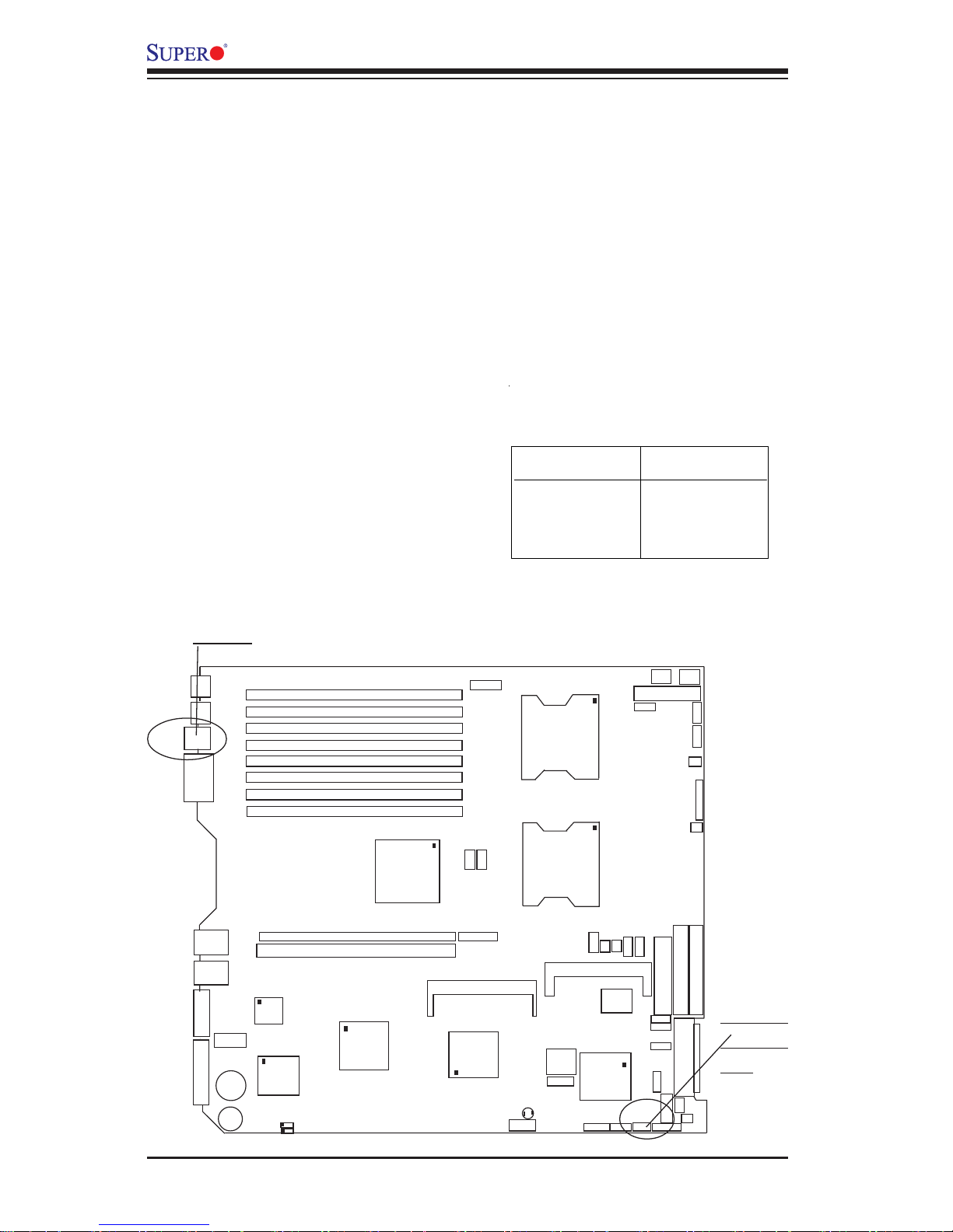
Power Button
The Power Button connection is
located on pins 1 and 2 of JF1.
Momentarily contacting both pins
will power on/off the system. This
button can also be configured to
function as a suspend button
(with a setting in BIOS - see Chapter 4). To turn off the power
when set to suspend mode, depress the button for at least 4
seconds. Refer to the table on the
right for pin definitions.
Pin
Number
1
2
Definition
PW_ ON
Ground
Power Button
Connector
Pin De finitions
(JF1)
Reset Button
The Reset Button connection is located on pins 3 and 4 of JF1. Attach it to the hardware reset
switch on the computer case.
Refer to the table on the right for
pin definitions.
Pin
Number
3
4
Definition
Reset
Ground
Reset Pin
Definitions
(JF1)
K
B
DIMM 4B
Mouse
USB
0/1
J14
C
O
M
1
DIMM 4A
DIMM 3B
DIMM 3A
DIMM 2B
DIMM 2A
DIMM 1B
DIMM 1A
G
L
A
N
1
G
L
A
N
2
VGA
S
C
S
I C
h
B
B
a
tte
ry
JP
G
1
(V
G
A
E
n
a
b
le
)
J
P
L
1
(L
A
N
E
n
a
ble)
R
A
G
E
-
X
G
L
A
N
C
T
R
L
P
X
H
V
G
A
C
T
R
L
P
C
I-E
x1
6
P
C
I-X
1
3
3
M
H
z
E
7
5
25
(T
u
m
w
a
te
r)
N
o
rth
B
rid
g
e
IC
H
5
R
(S
o
u
th
B
rid
g
e
)
Z
C
R
IPMI 2.0
BIOS
S I/O
7902
SCSI
CTRL
IDE #1
IDE #2
Floppy
SCSI Ch A
WOL
COM2
SCSI
Enable
USB2/3
JD2
JP9
CLR CMOS
Force PW-On
WOR
SPK
SW
SCSI
Ter. A
JPA1
JBT1
S
M
B
FAN5
S
A
T
A
1
SATA0
F
P
C
T
R
L
JF
1
FAN2
FAN1
20-PinPW
8-Pin
CPU
4-Pin
PW
PW SMB
PW
LED
Chas
Intru.
JL1
JWD
WD
CPU1
CPU2
JPA3
JPA2
S
C
S
I T
e
r. B
OH
J33
J34
J16
J7
J14
JD1
JA1
J5
J6
J12
F
A
N
4
J1B1
J1D1
J38
J32
J4
F
4
J
4
F
5
M
e
m
o
ry
S
p
e
e
d
(*N
o
te
:4
)
J11
PW
Fail
S
P
K
R
P
C
I-E
x4
JOH1
JW
O
R
JPF
JS
1
JS
2
JP
10
3RDPWDetect
Alarm
Reset
JP
1
1
F
A
N
3
Power Button
Overheat/Fan Fail LED
1
NIC1 LED
Reset Button
2
Power Fail LED
HDD LED
Power LED
Reset
Pwr
Vcc
Vcc
Vcc
Vcc
Ground
Ground
1920
Vcc
X
Ground
NMI
X
NIC2 LED
Vcc
Reset
PWR button
Page 34
2-14
X6DAR-8G/X6DAR-iG User's Manual
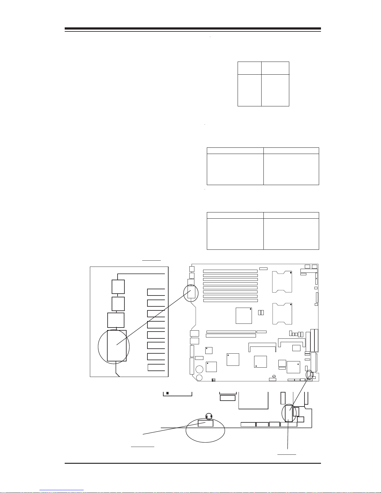
Universal Serial Bus
(USB0/1)
Two USB 2.0 ports (J16) are located beside the Mouse and COM1
ports. USB0 is the bottom connector and USB1 is the top connector.
See the table on the right for pin
definitions.
Universal Serial Bus Pin Definitions
Pin
Number Definition
1+5V
2P0 3P0+
4 Ground
5 N/A
Pin
Number Definition
1+5V
2P0 3P0+
4 Ground
5Key
USB0
USB1
Chassis Intrusion
A Chassis Intrusion header is located at JL1. Attach the appropriate cable to inform you of a chassis intrusion.
KB
DIMM 4B
Mouse
U
SB
0/1
J14
COM1
DIMM 4A
DIMM 3B
DIMM 3A
DIMM 2B
DIMM 2A
DIMM 1B
DIMM 1A
G
LAN1
G
LAN2
VGA
SCSI Ch B
Battery
JPG
1(VG
A Enable)
JPL1(LAN Enable)
RAG
E-
X
G
LAN
CTR
L
PXH
VG
A
CTRL
PCI-E x16
PCI-X 133M
H
z
E7525
(Tum
water)
North Bridge
ICH5R
(South
Bridge)
ZCR
IPMI 2.0
BIOS
S I/O
7902
SCSI
CTRL
ID
E
#
1
IDE #2
Floppy
SCSI Ch A
WOL
C
O
M
2
SCSI
Enable
USB2/3
JD2
JP9
CLR CMOS
Force PW-On
WOR
SPK
SW
SCSI
Ter. A
JPA1
JBT1
S
M
B
FAN5
SATA1
SATA0
F
P
C
T
R
L
J
F
1
FAN2
FAN1
20-PinPW
8-Pin
CPU
4-Pin
PW
PW SMB
PW
LED
Chas
Intru.
JL1
JWD
WD
CPU1
CPU2
JPA3
JPA2
S
C
S
I T
e
r. B
OH
J33
J34
J16
J7
J14
JD1
JA1
J5
J6
J12
FAN4
J1B1
J1D1
J38
J32
J4
F
4
J4
F
5
M
e
m
o
ry
S
p
e
e
d
(*N
o
te
:4
)
J11
PW
Fail
SPKR
PCI-Ex4
JOH1
JWOR
JPF
JS
1
JS
2
JP
1
0
3RDPWDetect
Alarm
Reset
JP
1
1
F
A
N
3
USB0/1
Chassis
Intrusion
Page 35
Chapter 2: Installation
2-15
Front Panel Universal
Serial Bus Headers
An Extra USB header: USB2/USB3
(JD2) can be used for front side
USB access. You will need a USB
cable to use the connections. Refer to the tables on the right for
pin definitions.
Front Panel Universal Serial Bus Pin
Definitions
Pin
Number Definition
1+5V
2P0 3P0+
4 Ground
5 N/A
FPUSB0/1 (JD2)
Serial Ports
COM Port1(J14) is located beside
the Back Panel USB0/1, and COM
Port 2 is located next to Chassis
Fan1. See the table on the right
for pin definitions.
K
B
DIMM 4B
Mouse
USB
0/1
J14
C
O
M
1
DIMM 4A
DIMM 3B
DIMM 3A
DIMM 2B
DIMM 2A
DIMM 1B
DIMM 1A
G
L
A
N
1
G
L
A
N
2
VGA
S
C
S
I C
h
B
B
a
tte
ry
JP
G
1
(V
G
A
E
n
a
b
le
)
JP
L
1
(L
A
N
E
n
a
b
le
)
R
A
G
E
-
X
G
L
A
N
C
T
R
L
P
X
H
V
G
A
C
T
R
L
P
C
I-E
x1
6
P
C
I-X
1
3
3
M
H
z
E
7
5
2
5
(T
u
m
w
a
te
r)
N
o
rth
B
rid
g
e
IC
H
5
R
(S
o
u
th
B
rid
g
e
)
Z
C
R
IPMI 2.0
BIOS
S I/O
7902
SCSI
CTRL
IDE #1
IDE #2
Floppy
SCSI Ch A
WOL
COM2
SCSI
Enable
USB2/3
JD2
JP9
CLR CMOS
Force PW-On
WOR
SPK
SW
SCSI
Ter. A
JPA1
JBT1
S
M
B
FAN5
S
A
T
A
1
SATA0
F
P
C
T
R
L
J
F
1
FAN2
FAN1
20-PinPW
8-Pin
CPU
4-Pin
PW
PW SMB
PW
LED
Chas
Intru.
JL1
JWD
WD
CPU1
CPU2
JPA3
JPA2
S
C
S
I T
e
r. B
OH
J33
J34
J16
J7
J14
JD1
JA1
J5
J6
J12
F
A
N
4
J1B1
J1D1
J38
J32
J4F
4
J4
F
5
M
e
m
o
ry
S
p
e
e
d
(*N
ote
:4
)
J11
PW
Fail
S
P
K
R
P
C
I-E
x4
JOH1
JW
O
R
JPF
JS
1
JS
2
JP
10
3RDPWDetect
Alarm
Reset
JP
1
1
F
A
N
3
KB
DIM
M
Mouse
USB
0/1
J14
C
O
M
1
DIM
M
DIM
M
DIM
M
DIM
M
DIM
M
DIM
M
DIM
M
J33
J34
J16
SCSI
CTRL
S
WOL
COM2
SCSI
Enable
USB2/3
JD2
CLR CMOS
SPK
SW
SCSI
Ter.
A
JPA1
JBT1
PW
LED
Chas
Intru.
JL1
JWD
WD
JPA2
OH
JD1
JA1
JOH1
FAN3
USB2/3
COM1
COM2
Serial Port Pin Definitions
(COM1)
Pin Number Definition
1 CD
2 RD
3 TD
4 DTR
5 Ground
Pin Number Definition
6 DSR
7 RTS
8 CTS
9 RI
Serial Port Pin Definitions
(COM2)
Pin Number Definition
1 CD
2 RD
3 TD
4 DTR
5 Ground
Pin Number Definition
6 DSR
7 RTS
8 CTS
9 RI
10 NC
Page 36
2-16
X6DAR-8G/X6DAR-iG User's Manual
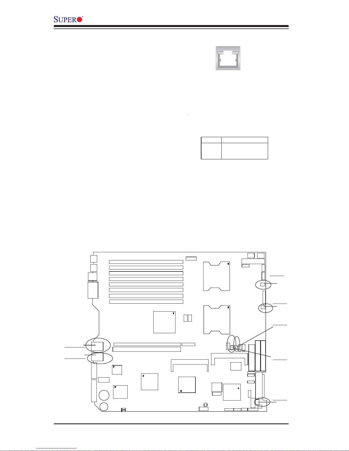
GLAN1/GLAN2 (GigabitEthernet Ports)
A G-bit Ethernet ports (designated
JLAN1/JLAN2) are located beside
the Video port on the IO backplane.
This ports accepts RJ45 type
cables.
K
B
DIMM 4B
Mouse
USB
0/1
J14
COM1
DIMM 4A
DIMM 3B
DIMM 3A
DIMM 2B
DIMM 2A
DIMM 1B
DIMM 1A
G
L
A
N
1
G
L
A
N
2
VGA
S
C
S
I C
h B
B
a
ttery
JP
G
1
(V
G
A
E
n
a
b
le
)
JP
L
1
(L
A
N
E
n
a
b
le)
R
A
G
E
-
X
G
L
A
N
C
T
R
L
P
X
H
V
G
A
C
T
R
L
P
C
I-E
x1
6
P
C
I-X
1
3
3M
H
z
E
752
5
(T
u
m
w
a
ter)
N
o
rth
B
ridg
e
IC
H
5
R
(S
o
u
th
B
rid
ge)
Z
C
R
IPMI 2.0
BIOS
S I/O
7902
SCSI
CTRL
IDE #1
IDE #2
Floppy
SCSI Ch A
WOL
C
O
M
2
SCSI
Enable
USB2/3
JD2
JP9
CLR CMOS
Force PW-On
WOR
SPK
SW
SCSI
Ter. A
JPA1
JBT1
S
M
B
FAN5
S
A
T
A
1
S
A
T
A
0
F
P
C
T
R
L
JF
1
FAN2
FAN1
20-PinPW
8-Pin
CPU
4-Pin
PW
PW SMB
PW
LED
Chas
Intru.
JL1
JWD
WD
CPU1
CPU2
JPA3
JPA2
SCSI Ter. B
OH
J33
J34
J16
J7
J14
JD1
JA1
J5
J6
J12
FAN4
J1B1
J1D1
J38
J32
J4
F
4
J4
F
5
M
e
m
o
ry
S
p
e
e
d
(*N
o
te
:4
)
J11
PW
Fail
S
P
K
R
P
C
I-E
x4
JOH1
JWOR
JPF
JS1
JS2
JP
10
3RDPWDetect
Alarm
Reset
JP
1
1
FAN
3
GLAN1
GLAN2
Fan1
Fan2
Fan4
Fan5
Fan3
Fan Headers
There are five fan headers (Fan 1
to Fan 5) on the X6DHR-8G/
X6DHR-iG. See the table on the
right for pin definitions. (The fan
speeds are controlled by Thermal
Management via BIOS. Please refer to the Hardware Monitoring
Section in the "Advanced Setting"
in BIOS.)
3-pin Fan Header Pin Definitions
(CPU and Chassis Fans )
Pin#
1
2
3
Definition
Ground (black)
+12V (red)
Tachometer
Caution: These fan headers use DC power.
Page 37
Chapter 2: Installation
2-17
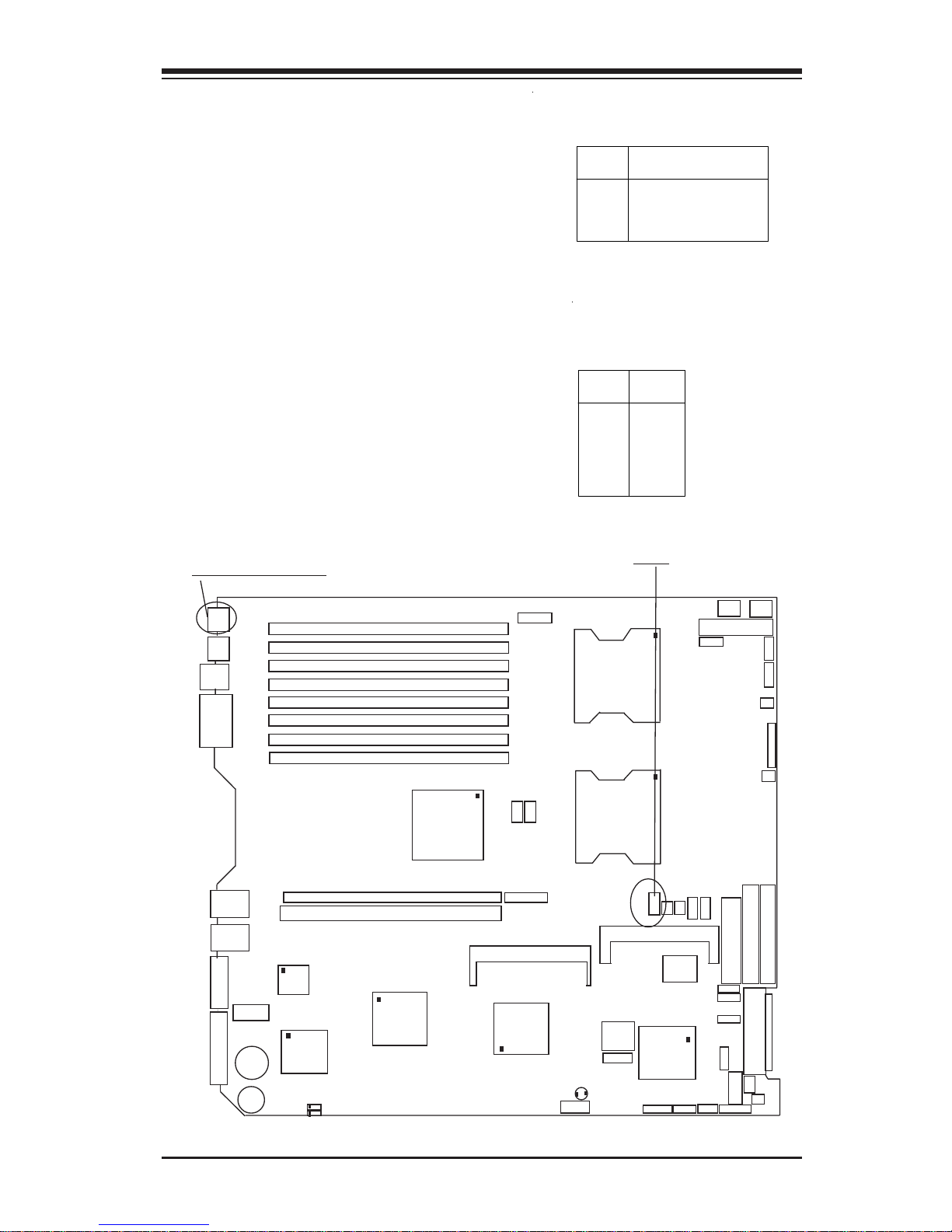
SMB
A System Management Bus
header is located at J11. Connect
the appropriate cable here to utilize SMB on your system.
ATX PS/2 Keyboard and
PS/2 Mouse Ports
The ATX PS/2 Keyboard(J34) and
PS/2 Mouse(J33) are located beside the USB0/1 Ports on the
backpanel. See the table at right
for pin definitions. (See Figure 23 for the locations of each.)
PS/2 Keyboard
and Mouse Port
Pin Definiti ons
(J34, J33)
Pin
Number
1
2
3
4
5
6
Definition
Data
NC
Ground
VCC
Clock
NC
KB
DIMM 4B
Mouse
USB
0/1
J14
C
O
M
1
DIMM 4A
DIMM 3B
DIMM 3A
DIMM 2B
DIMM 2A
DIMM 1B
DIMM 1A
GLAN1
GLAN2
VGA
SCSI Ch B
Battery
JPG1(VGA Enable)
JPL1(LAN Enable)
RAGEX
GLAN
CTRL
PXH
VGA
CTRL
PCI-E x16
PCI-X 133MHz
E7525
(Tumwater)
North Bridge
ICH5R
(South
Bridge)
ZCR
IPMI 2.0
BIOS
S I/O
7902
SCSI
CTRL
IDE #1
IDE #2
Floppy
SCSI Ch A
WOL
COM2
SCSI
Enable
USB2/3
JD2
JP9
CLR CMOS
Force PW-On
WOR
SPK
SW
SCSI
Ter. A
JPA1
JBT1
S
M
B
FAN5
SATA1
SATA0
F
P
C
T
R
L
JF1
FAN2
FAN1
20-PinPW
8-Pin
CPU
4-Pin
PW
PW SMB
PW
LED
Chas
Intru.
JL1
JWD
WD
CPU1
CPU2
JPA3
JPA2
SCSI Ter. B
OH
J33
J34
J16
J7
J14
JD1
JA1
J5
J6
J12
FAN
4
J1B1
J1D1
J38
J32
J4F
4
J4F
5
M
em
ory
S
peed
(*N
ote:4)
J11
PW
Fail
SPKR
PCI-Ex4
JOH1
JW
OR
JPF
JS1
JS2
JP
10
3RDPWDetect
Alarm
Reset
JP
11
FAN3
Keyboard/Mouse
SMB
SMB Header
Pin Definitions (J11)
Pin
Number
1
2
3
4
Definitio n
Data
Ground
Clock
No Connection
Page 38
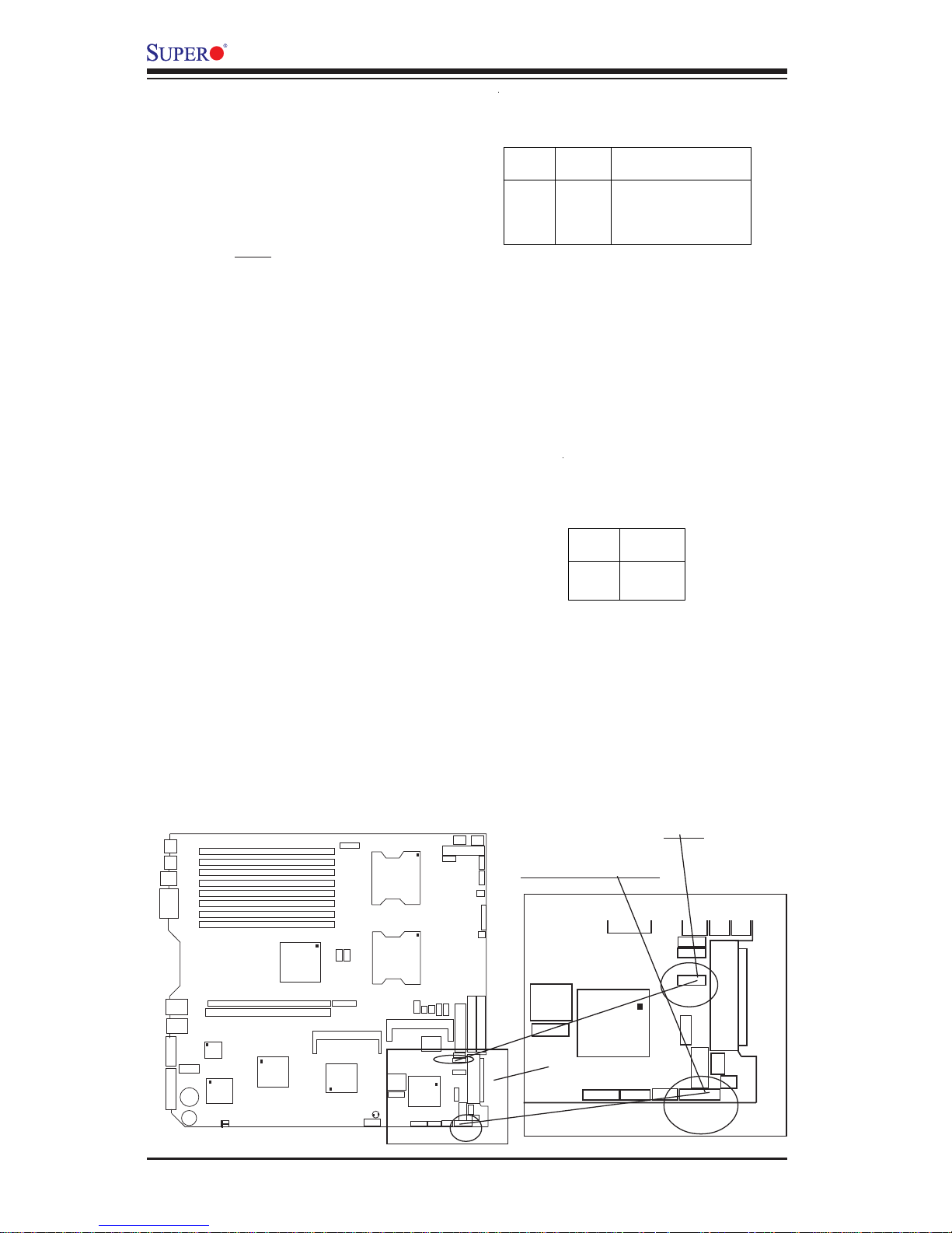
2-18
X6DAR-8G/X6DAR-iG User's Manual
Wake-On-Ring
The Wake-On-Ring header is designated JWOR1. This function allows your computer to receive
and "wake-up" by an incoming call
to the modem when in suspend
state. See the table on the right
for pin definitions. You must have
a Wake-On-Ring card and cable to
use this feature.
Wake-on-Ring
Pin Definitions
(JWOR1)
Pin
Number
1
2
Definition
Ground
Wake-up
Power LED/Speaker
On the JDI header, pins 1-3 are
for a power LED and pins 4-7 are
for the speaker. See the table on
the right for speaker pin definitions. Note: The speaker connector pins are for use with an external speaker. If you wish to use
the onboard speaker, you should
close pins 6-7 with a jumper.
Speaker Connector Pin
Definitions (J D 1)
Pin
Number
4
5
6
7
Function
+
Key
Defi n iti o n
Red wire, Speaker data
No connection
Key
Speaker data
K
B
DIMM 4B
Mouse
USB
0/1
J14
C
O
M
1
DIMM 4A
DIMM 3B
DIMM 3A
DIMM 2B
DIMM 2A
DIMM 1B
DIMM 1A
G
L
A
N
1
G
L
A
N
2
VGA
S
C
S
I C
h
B
B
a
tte
ry
JP
G
1
(V
G
A
E
n
a
b
le
)
JP
L
1
(L
A
N
E
n
a
b
le
)
R
A
G
E
-
X
G
L
A
N
C
T
R
L
P
X
H
V
G
A
C
T
R
L
P
C
I-E
x1
6
P
C
I-X
1
3
3
M
H
z
E
7
5
2
5
(T
u
m
w
a
te
r)
N
o
rth
B
rid
g
e
IC
H
5
R
(S
o
u
th
B
rid
g
e
)
Z
C
R
IPMI 2.0
BIOS
S I/O
7902
SCSI
CTRL
IDE #1
IDE #2
Floppy
SCSI Ch A
WOL
COM2
SCSI
Enable
USB2/3
JD2
JP9
CLR CMOS
Force PW-On
WOR
SPK
SW
SCSI
Ter. A
JPA1
JBT1
S
M
B
FAN5
S
A
T
A
1
SATA0
F
P
C
T
R
L
JF
1
FAN2
FAN1
20-PinPW
8-Pin
CPU
4-Pin
PW
PW SMB
PW
LED
Chas
Intru.
JL1
JWD
WD
CPU1
CPU2
JPA3
JPA2
S
C
S
I T
e
r. B
OH
J33
J34
J16
J7
J14
JD1
JA1
J5
J6
J12
F
A
N
4
J1B1
J1D1
J38
J32
J4
F
4
J4
F
5
M
e
m
o
ry
S
p
e
e
d
(*N
o
te
:4
)
J11
PW
Fail
S
P
K
R
P
C
I-E
x4
JOH1
JW
O
R
JPF
JS
1
JS
2
JP
1
0
3RDPWDetect
Alarm
Reset
JP
1
1
F
A
N
3
BIOS
7902
SCSI
CTRL
SCSI Ch A
WOL
COM2
e
Force PW-On
WOR
SPK
SW
SCSI
Ter. A
JPA1
PW
LED
Chas
Intru.
JL1
JWD
WD
JPA3
JPA2
SCSI Ter. B
OH
JD1
JA1
J5
J6
J12
JOH1
JWOR
JPF
FAN3
WOR
PWRLED/Speaker
Page 39
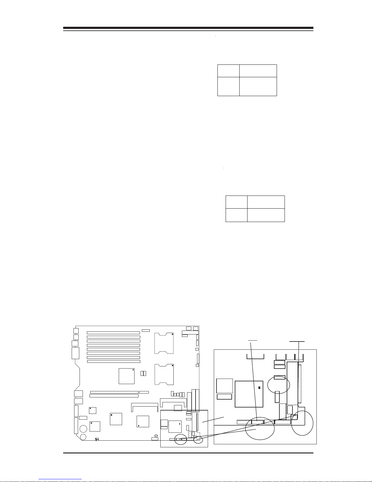
Chapter 2: Installation
2-19
Pin
Number
1
2
3
Defin itio n
+5V Standby
Ground
Wake-up
Wake-On-LAN Pin
Definitions (WOL)
Wake-On-LAN
The Wake-On-LAN header is designated WOL. See the table on the
right for pin definitions. You must
enable the LAN Wake-Up setting in
BIOS to use this feature. You
must also have a LAN card with a
Wake-on-LAN connector and
cable.
Overheat LED (JOH1)
Connect an LED to the JOH1
header to provide warning of
chassis overheating. See the
table on the right for pin definitions.
Pin
Number
1
2
Defin itio n
+5V
OH A c tiv e
Overheat LED
Pin Definitions (JOH1)
K
B
DIMM 4B
Mouse
USB
0/1
J14
C
O
M
1
DIMM 4A
DIMM 3B
DIMM 3A
DIMM 2B
DIMM 2A
DIMM 1B
DIMM 1A
G
L
A
N
1
G
L
A
N
2
VGA
S
C
S
I C
h
B
B
a
tte
ry
JP
G
1
(V
G
A
E
n
a
b
le
)
JP
L
1
(L
A
N
E
n
a
b
le
)
R
A
G
E
-
X
G
L
A
N
C
T
R
L
P
X
H
V
G
A
C
T
R
L
P
C
I-E
x1
6
P
C
I-X
1
3
3
M
H
z
E
7
5
25
(T
u
m
w
a
te
r)
N
o
rth
B
rid
g
e
IC
H
5
R
(S
o
u
th
B
rid
g
e
)
Z
C
R
IPMI 2.0
BIOS
S I/O
7902
SCSI
CTRL
IDE #1
IDE #2
Floppy
SCSI Ch A
WOL
COM2
SCSI
Enable
USB2/3
JD2
JP9
CLR CMOS
Force PW-On
WOR
SPK
SW
SCSI
Ter. A
JPA1
JBT1
S
M
B
FAN5
S
A
T
A
1
SATA0
F
P
C
T
R
L
JF
1
FAN2
FAN1
20-PinPW
8-Pin
CPU
4-Pin
PW
PW SMB
PW
LED
Chas
Intru.
JL1
JWD
WD
CPU1
CPU2
JPA3
JPA2
S
C
S
I T
e
r. B
OH
J33
J34
J16
J7
J14
JD1
JA1
J5
J6
J12
F
A
N
4
J1B1
J1D1
J38
J32
J4
F
4
J4
F
5
M
e
m
o
ry
S
p
e
e
d
(*N
o
te
:4
)
J11
PW
Fail
S
P
K
R
P
C
I-E
x4
JOH1
JW
O
R
JPF
JS
1
JS
2
JP
1
0
3RDPWDetect
Alarm
Reset
JP
1
1
F
A
N
3
BIOS
7902
SCSI
CTRL
SCSI Ch A
WOL
COM2
e
Force PW-On
WOR
SPK
SW
SCSI
Ter. A
JPA1
PW
LED
Chas
Intru.
JL1
JWD
WD
JPA3
JPA2
SCSI Ter. B
OH
JD1
JA1
J5
J6
J12
JOH1
JWOR
JPF
FAN3
WOL
OH
Page 40
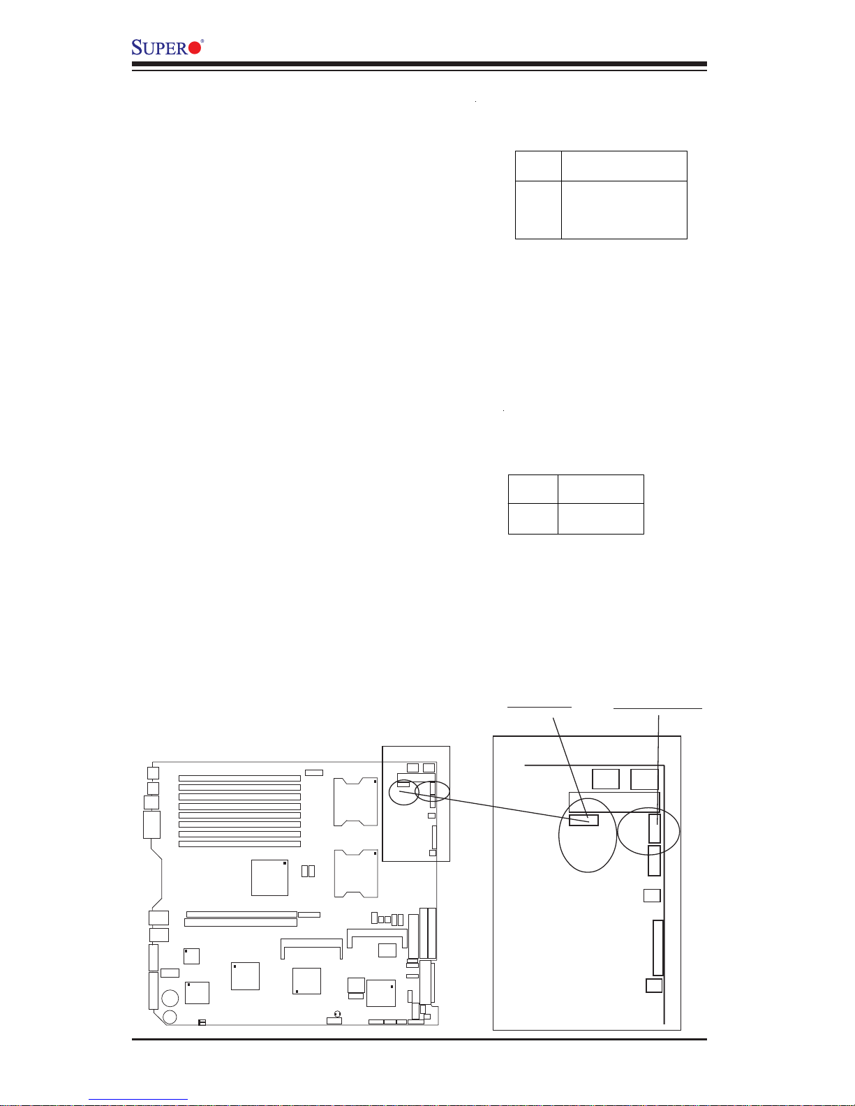
2-20
X6DAR-8G/X6DAR-iG User's Manual
Power Fault
Connect a cable from your power
supply to the Power Fail header
(JP9) to provide warning of power
supply failure. This warning signal is passed through the
PWR_LED pin to indicate of a
power failure on the chassis. See
the table on the right for pin definitions.
Power Fail
Pin Definitions (JP9)
Pin
Number
1
2
3
4
Definition
PWR 1 Fail Signal
PWR 2 Fail Signal
PWR 3 Fail Signal
Signal: Alarm Reset
Note: This feature is only available when using
redundant Supermicro power supplies.
Alarm Reset
The system will notify you in the
event of a power supply failure.
This feature (JP11) assumes that
Supermicro redundant power supply units are installed in the chassis. If you only have a single
power supply installed, you should
leave the pins open (the default
setting) to prevent false alarms.
See the table on the right for
jumper settings.
Jumper
Position
Open
Short
Definition
Normal(*default)
Clear Alarm
Alarm Reset
(JP11)
K
B
DIMM 4B
Mouse
USB
0/1
J14
C
O
M
1
DIMM 4A
DIMM 3B
DIMM 3A
DIMM 2B
DIMM 2A
DIMM 1B
DIMM 1A
G
L
A
N
1
G
L
A
N
2
VGA
S
C
S
I C
h
B
B
a
tte
ry
JP
G
1
(V
G
A
E
n
a
b
le
)
J
P
L
1
(L
A
N
E
n
a
b
le
)
R
A
G
E
-
X
G
L
A
N
C
T
R
L
P
X
H
V
G
A
C
T
R
L
P
C
I-E
x1
6
P
C
I-X
1
3
3
M
H
z
E
75
2
5
(T
u
m
w
a
te
r)
N
o
rth
B
rid
g
e
IC
H
5
R
(S
o
u
th
B
rid
g
e
)
Z
C
R
IPMI 2.0
BIOS
S I/O
7902
SCSI
CTRL
IDE #1
IDE #2
Floppy
SCSI Ch A
WOL
COM2
SCSI
Enable
USB2/3
JD2
JP9
CLR CMOS
Force PW-On
WOR
SPK
SW
SCSI
Ter. A
JPA1
JBT1
S
M
B
FAN5
S
A
T
A
1
SATA0
F
P
C
T
R
L
J
F
1
FAN2
FAN1
20-PinPW
8-Pin
CPU
4-Pin
PW
PW SMB
PW
LED
Chas
Intru.
JL1
JWD
WD
CPU1
CPU2
JPA3
JPA2
S
C
S
I T
e
r. B
OH
J33
J34
J16
J7
J14
JD1
JA1
J5
J6
J12
F
A
N
4
J1B1
J1D1
J38
J32
J4
F
4
J4
F
5
M
e
m
o
ry
S
p
e
e
d
(*N
o
te
:4
)
J11
PW
Fail
S
P
K
R
P
C
I-E
x4
JOH1
JW
O
R
JPF
JS
1
JS
2
JP
1
0
3RDPWDetect
Alarm
Reset
JP
1
1
F
A
N
3
JP9
FP CTRL
JF1
FAN2
FAN1
20-PinPW
8-Pin
CPU
4-Pin
PW
J1B1
J1D1
J38
PW
Fail
JP10
3RDPWDetect
Alarm
Reset
JP11
PWR Fail
Alarm Reset
Page 41
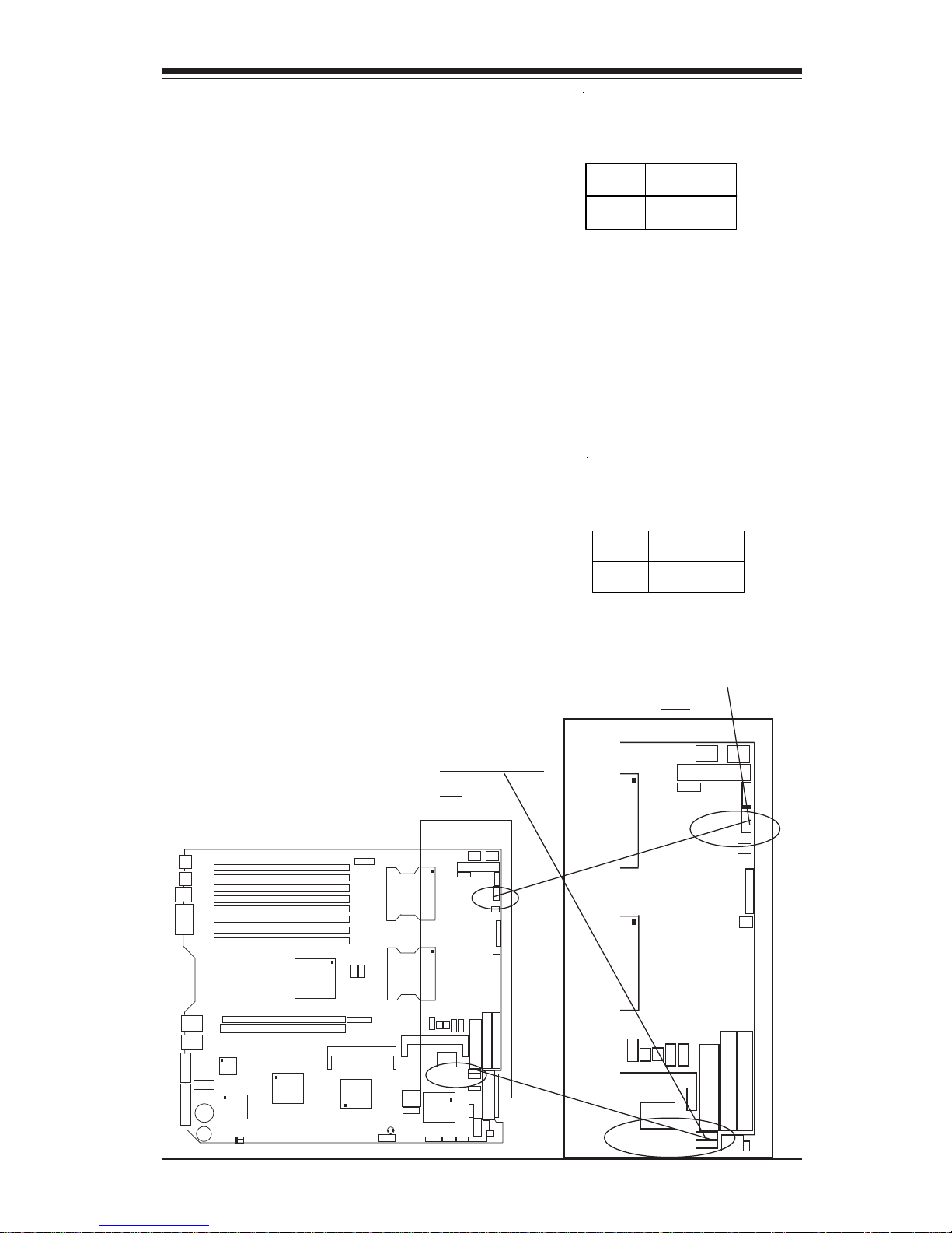
Chapter 2: Installation
2-21
S I/O
IDE #1
IDE #2
Floppy
A
JP9
Force PW-On
WOR
S
M
B
FAN5
SATA
1
SATA0
F
P
C
T
R
L
JF
1
FAN2
FAN1
20-PinPW
8-Pin
CPU
4-Pin
PW
J5
J6
J12
F
A
N
4
J1B1
J1D1
J38
J11
PW
Fail
JPF
JS1
JS2
JP
1
0
3RDPWDetect
Alarm
Reset
JP
11
3rd PWR Supply PWR
Fault Detect (JP10)
The system can notify you in the
event of a power supply failure.
This feature assumes that three
power supply units are installed in
the chassis, with one acting as a
backup. If you only have one or
two power supply units installed,
you should disable this (the default
setting) with JP10 to prevent false
alarms.
Jumper
Position
Open
Closed
Definition
Disabled
Enabled
3rd PWR Supply PWR
Fault Detect
Jumper Settings (JP10)
K
B
DIMM 4B
Mouse
USB
0/1
J14
C
O
M
1
DIMM 4A
DIMM 3B
DIMM 3A
DIMM 2B
DIMM 2A
DIMM 1B
DIMM 1A
G
L
A
N
1
G
L
A
N
2
VGA
S
C
S
I C
h
B
B
a
tte
ry
JP
G
1
(V
G
A
E
n
a
b
le
)
J
P
L
1(L
A
N
E
n
a
b
le
)
R
A
G
E
-
X
G
L
A
N
C
T
R
L
P
X
H
V
G
A
C
T
R
L
P
C
I-E
x1
6
P
C
I-X
1
3
3
M
H
z
E
75
2
5
(T
u
m
w
a
te
r)
N
o
rth
B
rid
g
e
IC
H
5
R
(S
o
u
th
B
rid
g
e
)
Z
C
R
IPMI 2.0
BIOS
S I/O
7902
SCSI
CTRL
IDE #1
IDE #2
Floppy
SCSI Ch A
WOL
COM2
SCSI
Enable
USB2/3
JD2
JP9
CLR CMOS
Force PW-On
WOR
SPK
SW
SCSI
Ter. A
JPA1
JBT1
S
M
B
FAN5
S
A
T
A
1
SATA0
F
P
C
T
R
L
JF
1
FAN2
FAN1
20-PinPW
8-Pin
CPU
4-Pin
PW
PW SMB
PW
LED
Chas
Intru.
JL1
JWD
WD
CPU1
CPU2
JPA3
JPA2
S
C
S
I T
e
r. B
OH
J33
J34
J16
J7
J14
JD1
JA1
J5
J6
J12
F
A
N
4
J1B1
J1D1
J38
J32
J4
F
4
J
4
F
5
M
e
m
o
ry
S
p
e
e
d
(*N
o
te
:4
)
J11
PW
Fail
S
P
K
R
P
C
I-E
x4
JOH1
JW
O
R
JPF
JS
1
JS
2
JP
10
3RDPWDetect
Alarm
Reset
JP
1
1
F
A
N
3
3rd PWR Detect
Power Force-On
Jumper JPF allows you to enable or
disable the function of Power
Force-On. If enabled, the power
will always stay on automatically.
If this function disabled, the user
needs to press the power button to
power on the system.
Jumper
Position
Off
On
Definition
Normal
Force On
Power Force-On
(JPF)
PWR ForceOn
Page 42
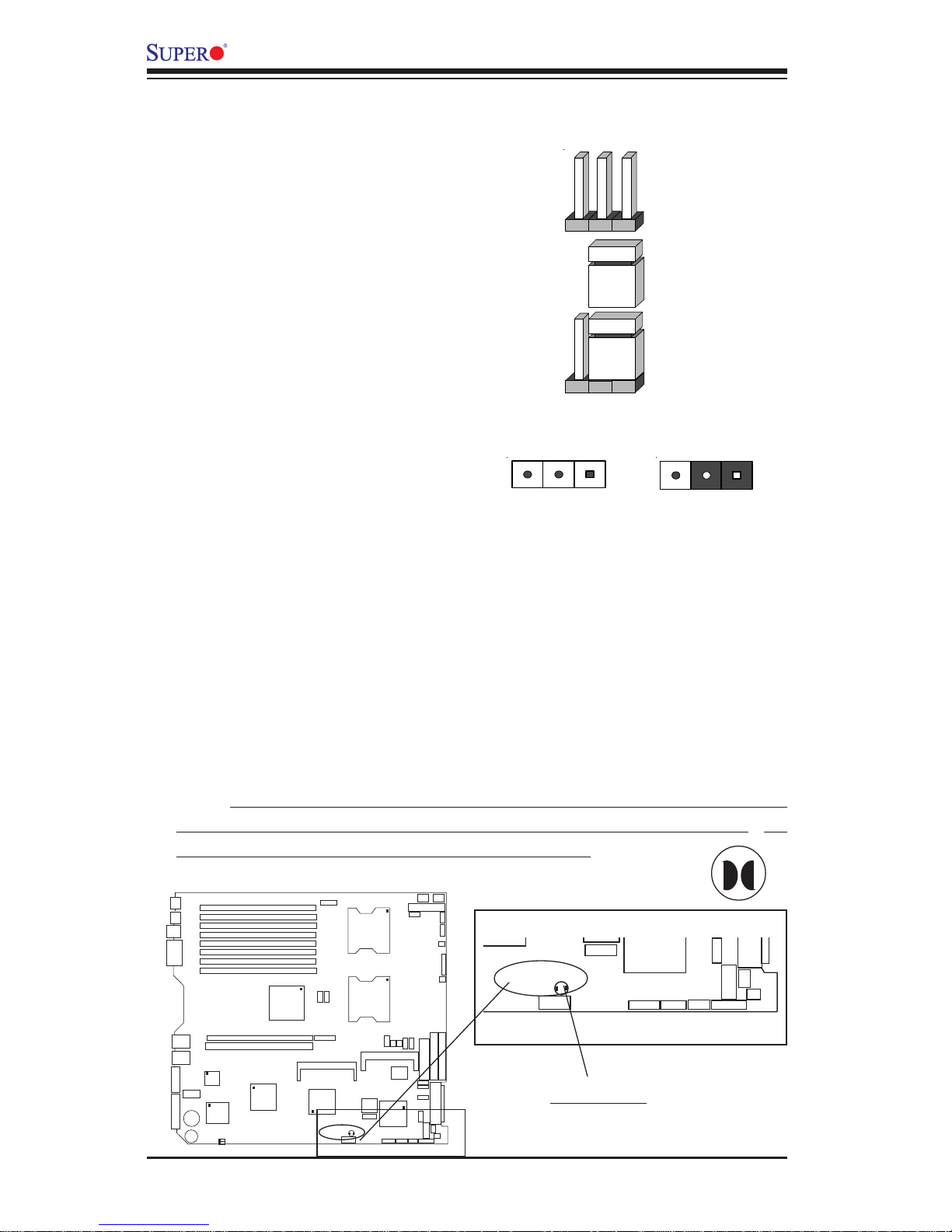
2-22
X6DAR-8G/X6DAR-iG User's Manual
Connector
Pins
Jumper
Cap
Setting
Pin 1-2 short
3 2 1
3 2 1
CMOS Clear
JBT1 is used to clear CMOS. Instead of pins, this "jumper" consists of
contact pads to prevent the accidental clearing of CMOS. To clear CMOS,
use a metal object such as a small screwdriver to touch both pads at the
same time to short the connection. Always remove the AC power cord
from the system before clearing CMOS. JBT1 is located near the FPUSB0/
1 headers on the motherboard.
Note: For an ATX power supply, you must completely shut down the system, remove the AC power cord and then short JBT1 to clear CMOS. Do
not use the PW_ON connector to clear CMOS.
KB
DIMM 4B
M
ouse
U
S
B
0
/1
J14
COM
1
DIMM 4A
DIMM 3B
DIMM 3A
DIMM 2B
DIMM 2A
DIMM 1B
DIMM 1A
GLAN1
GLAN2
V
G
A
SCSI Ch B
Battery
JPG1(VGA Enable)
JPL1(LAN Enable)
RAGEX
GLAN
CTRL
PXH
VGA
CTRL
PCI-E x16
PCI-X 133MHz
E7525
(Tumwater)
North Bridge
ICH5R
(South
Bridge)
ZCR
IPMI 2.0
BIOS
S I/O
7902
SCSI
CTRL
ID
E
#
1
IDE #2
Floppy
SCSI Ch A
WOL
C
O
M
2
SCSI
Enable
USB2/3
JD2
JP9
CLR CMOS
Force PW-On
WOR
SPK
SW
SCSI
Ter. A
JPA1
JBT1
S
M
B
FAN5
SATA1
SATA0
F
P
C
T
R
L
JF
1
FAN2
FAN1
20-PinPW
8-Pin
CPU
4-Pin
PW
PW SMB
PW
LED
Chas
Intru.
JL1
JWD
WD
CPU1
CPU2
JPA3
JPA2
S
C
S
I T
e
r. B
OH
J33
J34
J16
J7
J
1
4
JD1
JA1
J5
J6
J12
FAN4
J1B1
J1D1
J38
J32
J4
F
4
J4
F
5
M
e
m
o
ry
S
p
e
e
d
(*N
o
te
:4
)
J11
PW
Fail
SPKR
PCI-Ex4
JOH1
JW
O
R
JP
F
JS
1
JS
2
JP
10
3RDPWDetect
Alarm
Reset
JP
1
1
FAN3
SCSI
CTRL
S
WOL
C
O
M
2
SCSI
Enable
USB2/3
JD2
CLR CMOS
SPK
SW
SCSI
Ter.
A
JPA1
JBT1
PW
LED
Chas
Intru.
JL1
JWD
WD
JPA2
OH
JD1
JA1
JOH1
F
A
N
3
Clear CMOS
2-6 Jumper Settings
Explanation of
Jumpers
To modify the operation of the
motherboard, jumpers can be
used to choose between
optional settings. Jumpers
create shorts between two pins
to change the function of the
connector. Pin 1 is identified
with a square solder pad on
the printed circuit board. See
the motherboard layout pages
for jumper locations.
Note: On two pin jumpers,
"Closed" means the jumper is
on and "Open" means the
jumper is off the pins.
Page 43
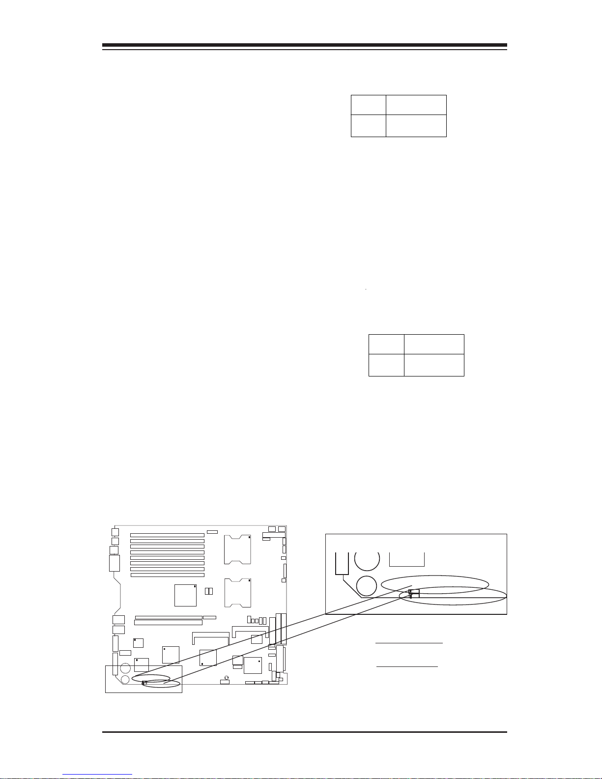
Chapter 2: Installation
2-23
GLAN Enable/Disable
JPL1 enables or disables the
GLAN port(s) on the motherboard.
See the table on the right for
jumper settings. The default setting is enabled.
Jumper
Position
Pins 1-2
Pins 2-3
Definition
Enabled
Disabled
GLAN
Enable/Disable
Jumper Settings
(JPL1)
VGA Enable/Disable
JPG1 enables or disables the VGA
Connector on the motherboard.
See the table on the right for
jumper settings. The default setting is enabled.
Jumper
Position
Pins 1-2
Pins 2-3
Definition
Enabled
Disabled
VGA
Enable/Disable
Jumper Settings
(JPG1)
SC
S
Battery
JPG1(VGA Enable)
JPL1(LAN Enable)
X
J14
SPKR
KB
DIMM 4B
M
ouse
U
S
B
0
/1
J14
COM1
DIMM 4A
DIMM 3B
DIMM 3A
DIMM 2B
DIMM 2A
DIMM 1B
DIMM 1A
GLAN1
GLAN2
V
G
A
SCSI Ch B
Battery
JPG1(VGA Enable)
JPL1(LAN Enable)
RAGEX
GLAN
CTRL
PXH
VGA
CTRL
PCI-E x16
PCI-X 133MHz
E7525
(Tumwater)
North Bridge
ICH5R
(South
Bridge)
ZCR
IPMI 2.0
BIOS
S I/O
7902
SCSI
CTRL
ID
E
#
1
IDE #2
Floppy
SCSI Ch A
WOL
C
O
M
2
SCSI
Enable
USB2/3
JD2
JP9
CLR CMOS
Force PW-On
WOR
SPK
SW
SCSI
Ter. A
JPA1
JBT1
S
M
B
FAN5
SATA1
SATA0
F
P
C
T
R
L
J
F
1
FAN2
FAN1
20-PinPW
8-Pin
CPU
4-Pin
PW
PW SMB
PW
LED
Chas
Intru.
JL1
JWD
WD
CPU1
CPU2
JPA3
JPA2
S
C
S
I T
e
r. B
OH
J33
J34
J16
J7
J
1
4
JD1
JA1
J5
J6
J12
FAN4
J1B1
J1D1
J38
J32
J4
F
4
J4
F
5
M
e
m
o
ry
S
p
e
e
d
(*N
o
te
:4
)
J1
1
PW
Fail
SPKR
PCI-Ex4
JOH1
JW
O
R
JP
F
JS
1
JS
2
JP
1
0
3RDPWDetect
Alarm
Reset
JP
1
1
FAN3
GLAN Enable
VGA Enable
Page 44
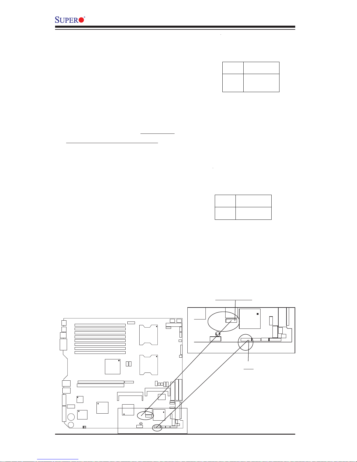
2-24
X6DAR-8G/X6DAR-iG User's Manual
SCSI Enable/Disable
(*X6DAR-8G Only)
Jumper JPA1 allows you to enable
or disable the SCSI Controller. The
default setting is pins 1-2 to enable
all four headers. See the table on
the right for jumper settings.
Watch Dog
JWD controls Watch Dog, a system
monitor that takes action when a
software application freezes the
system. Pins 1-2 will have WD reset the system if a program
freezes. Pins 2-3 will generate a
non-maskable interrupt for the program that has frozen (requires software implementation). Watch Dog
must also be enabled in BIOS.
Jumper
Position
Pins 1-2
Pins 2-3
Open
Definition
WD to Reset
WD to NMI
Disabled
Watch Dog
Jumper Settings (JWD)
K
B
DIMM 4B
Mouse
USB
0/1
J14
C
O
M
1
DIMM 4A
DIMM 3B
DIMM 3A
DIMM 2B
DIMM 2A
DIMM 1B
DIMM 1A
G
L
A
N
1
G
L
A
N
2
VGA
S
C
S
I C
h
B
B
a
tte
ry
JP
G
1
(V
G
A
E
n
a
b
le
)
J
P
L
1
(L
A
N
E
n
a
b
le
)
R
A
G
E
-
X
G
L
A
N
C
T
R
L
P
X
H
V
G
A
C
T
R
L
P
C
I-E
x1
6
P
C
I-X
1
3
3
M
H
z
E
75
2
5
(T
u
m
w
a
te
r)
N
o
rth
B
rid
g
e
IC
H
5
R
(S
o
u
th
B
rid
g
e
)
Z
C
R
IPMI 2.0
BIOS
S I/O
7902
SCSI
CTRL
IDE #1
IDE #2
Floppy
SCSI Ch A
WOL
COM2
SCSI
Enable
USB2/3
JD2
JP9
CLR CMOS
Force PW-On
WOR
SPK
SW
SCSI
Ter. A
JPA1
JBT1
S
M
B
FAN5
S
A
T
A
1
SATA0
F
P
C
T
R
L
J
F
1
FAN2
FAN1
20-PinPW
8-Pin
CPU
4-Pin
PW
PW SMB
PW
LED
Chas
Intru.
JL1
JWD
WD
CPU1
CPU2
JPA3
JPA2
S
C
S
I T
e
r. B
OH
J33
J34
J16
J7
J14
JD1
JA1
J5
J6
J12
F
A
N
4
J1B1
J1D1
J38
J32
J4
F
4
J4
F
5
M
e
m
o
ry
S
p
e
e
d
(*N
o
te
:4
)
J11
PW
Fail
S
P
K
R
P
C
I-E
x4
JOH1
JW
O
R
JPF
JS
1
JS
2
JP
1
0
3RDPWDetect
Alarm
Reset
JP
1
1
F
A
N
3
uth
dge)
BIOS
7902
SCSI
CTRL
SCSI
WOL
COM2
SCSI
Enable
USB2/3
JD2
LR CMOS
SPK
SW
SCSI
Ter. A
JPA1
JBT1
PW
LED
Chas
Intru.
JL1
JWD
WD
JPA3
JPA2
SCSI
Ter.
B
OH
JD1
JA1
JOH1
FAN3
SCSI Enable
WD
Jumper
Position
Pins 1-2
Pins 2-3
Definition
Enabled
Disabled
SCSI Enable/Disable
Jumper Settings
(JPA1)
Page 45
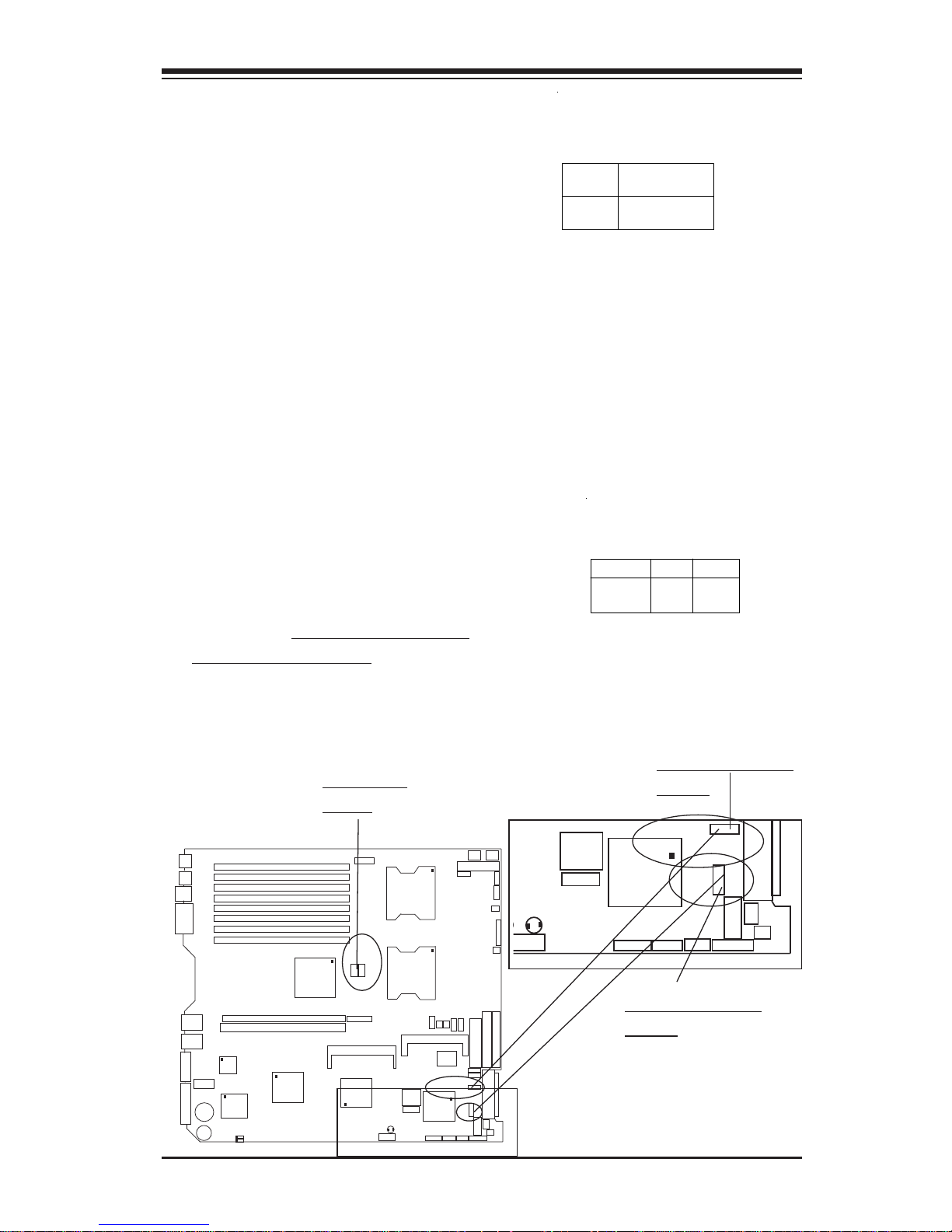
Chapter 2: Installation
2-25
BIOS
7902
SCSI
CTRL
SCSI C
h
WOL
COM2
CSI
nable
/3
D2
S
SPK
SW
SCSI
Ter. A
JPA1
BT1
PW
LED
Chas
Intru.
JL1
JWD
WD
JPA3
JPA2
SCSI Ter. B
OH
JD1
JA1
JOH1
JWOR
FAN3
SCSI Termination Enable/
Disable
Jumpers JPA2 and JPA3 allow you
to enable or disable termination for
the SCSI connectors. Jumper JPA2
controls SCSI channel A and JPA3
is for SCSI channel B. The default
setting is open to enable (terminate)
both SCSI channels. (For SCSI to
function properly, please do not
change the default setting.) See the
table on the right for jumper settings.
Jumper
Position
*Open
Closed
Definition
Enabled
Disabled
SCSI Channel Termination
Enable/Disable
Jumper Settings
(JPA2, JPA3)
(*X6DAR-8G Only)
(*Default: Open. Please do not change
the default setting.)
K
B
DIMM 4B
Mouse
USB
0/1
J14
C
O
M
1
DIMM 4A
DIMM 3B
DIMM 3A
DIMM 2B
DIMM 2A
DIMM 1B
DIMM 1A
G
L
A
N
1
G
L
A
N
2
VGA
S
C
S
I C
h
B
B
a
tte
ry
JP
G
1
(V
G
A
E
n
a
b
le
)
J
P
L
1(L
A
N
E
n
a
b
le
)
R
A
G
E
-
X
G
L
A
N
C
T
R
L
P
X
H
V
G
A
C
T
R
L
P
C
I-E
x1
6
P
C
I-X
1
3
3
M
H
z
E
75
2
5
(T
u
m
w
a
te
r)
N
o
rth
B
rid
g
e
IC
H
5
R
(S
o
u
th
B
rid
g
e
)
Z
C
R
IPMI 2.0
BIOS
S I/O
7902
SCSI
CTRL
IDE #1
IDE #2
Floppy
SCSI Ch A
WOL
COM2
SCSI
Enable
USB2/3
JD2
JP9
CLR CMOS
Force PW-On
WOR
SPK
SW
SCSI
Ter. A
JPA1
JBT1
S
M
B
FAN5
S
A
T
A
1
SATA0
F
P
C
T
R
L
JF
1
FAN2
FAN1
20-PinPW
8-Pin
CPU
4-Pin
PW
PW SMB
PW
LED
Chas
Intru.
JL1
JWD
WD
CPU1
CPU2
JPA3
JPA2
S
C
S
I T
e
r. B
OH
J33
J34
J16
J7
J14
JD1
JA1
J5
J6
J12
F
A
N
4
J1B1
J1D1
J38
J32
J4
F
4
J
4
F
5
M
e
m
o
ry
S
p
e
e
d
(*N
o
te
:4
)
J11
PW
Fail
S
P
K
R
P
C
I-E
x4
JOH1
JW
O
R
JPF
JS
1
JS
2
JP
10
3RDPWDetect
Alarm
Reset
JP
1
1
F
A
N
3
SCSI Ch.A Term.
Enable
SCSI Ch.B Term.
Enable
PLLSEL Select
J4F4/J4F5 allows the user to select PLLSEL (memory speed). See
the table on the right for jumper
definitions. (*The Default setting
is: BIOS Auto Detect).
DDR
333 MHz
266MHz
J4F4 J4F5
Closed Closed
Open Open
PLLSEL Select
Jumper Settings
(J4F4/J4F5)
(*Default:BIOS Auto
Detect)
PLLSEL
Select
Page 46
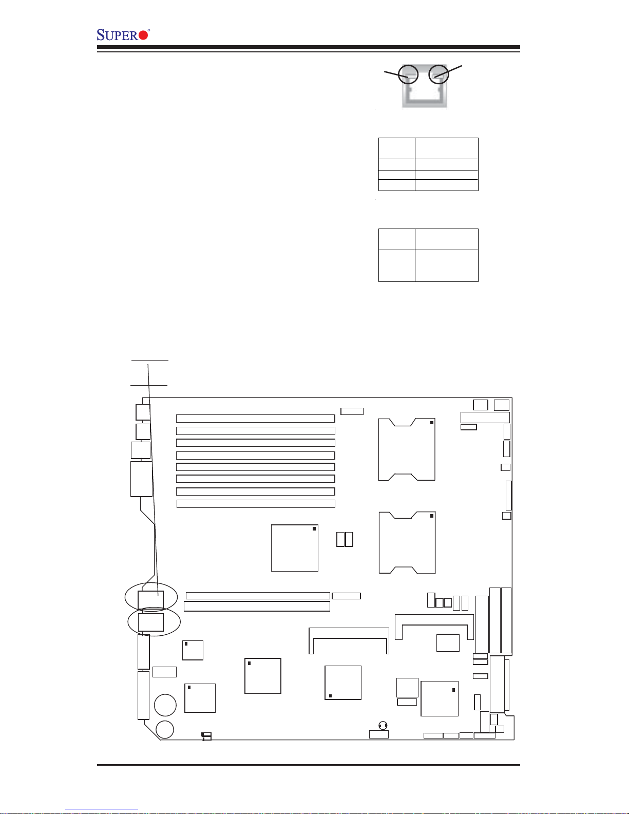
2-26
X6DAR-8G/X6DAR-iG User's Manual
2-7 Onboard Indicators
GLAN LEDs
The Gigabit Ethernet LAN ports (located beside the Video port) has
two LEDs. The yellow LED indicates activity while the other LED
may be green, amber or off to indicate the speed of the connection.
See the table at right for the functions associated with the second
LED.
LED
Color
Off
Green
Amber
Definition
No Connection
10/100 MHz
1 GHz
1 Gb LAN Right LED
Indicator (Speed LED)
Right
LED
Color
Amber
Definition
Blinking
10/100MHz/
1GHz
1 Gb LAN Left LED
Indicator(Activity LED)
Left
KB
DIMM 4B
Mouse
USB
0/1
J14
C
O
M
1
DIMM 4A
DIMM 3B
DIMM 3A
DIMM 2B
DIMM 2A
DIMM 1B
DIMM 1A
GLAN1
GLAN2
VGA
SCSI Ch B
Battery
JPG1(VGA Enable)
JPL1(LAN Enable)
RAGEX
GLAN
CTRL
PXH
VGA
CTRL
PCI-E x16
PCI-X 133MHz
E7525
(Tumwater)
North Bridge
ICH5R
(South
Bridge)
ZCR
IPMI 2.0
BIOS
S I/O
7902
SCSI
CTRL
IDE #1
IDE #2
Floppy
SCSI Ch A
WOL
COM2
SCSI
Enable
USB2/3
JD2
JP9
CLR CMOS
Force PW-On
WOR
SPK
SW
SCSI
Ter. A
JPA1
JBT1
S
M
B
FAN5
SATA1
SATA0
F
P
C
T
R
L
JF
1
FAN2
FAN1
20-PinPW
8-Pin
CPU
4-Pin
PW
PW SMB
PW
LED
Chas
Intru.
JL1
JWD
WD
CPU1
CPU2
JPA3
JPA2
SCSI Ter. B
OH
J33
J34
J16
J7
J14
JD1
JA1
J5
J6
J12
FAN
4
J1B1
J1D1
J38
J32
J4F
4
J4F
5
M
em
ory
S
peed
(*N
ote:4)
J11
PW
Fail
SPKR
PCI-Ex4
JOH1
JW
OR
JPF
JS1
JS2
JP
10
3RDPWDetect
Alarm
Reset
JP
1
1
FAN3
GLAN1
GLAN2
Page 47
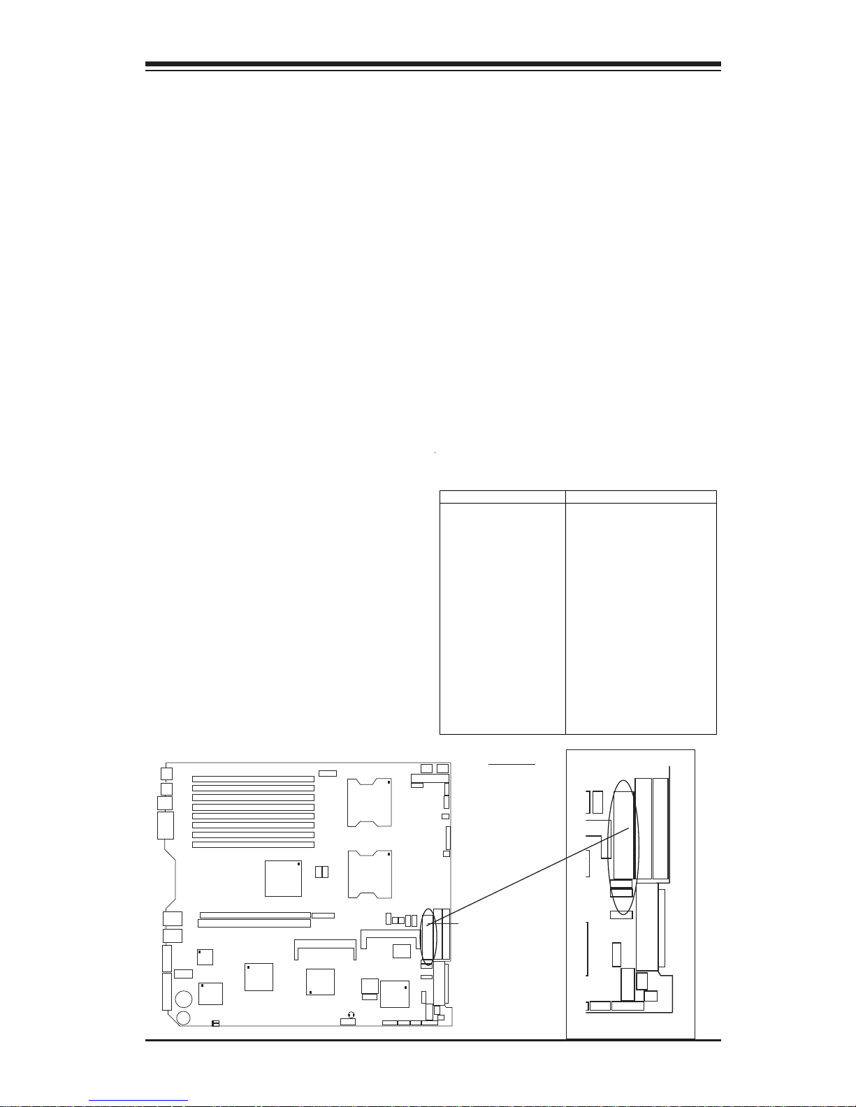
Chapter 2: Installation
2-27
Pin Number Function
1 GND
3 GND
5 Key
7 GND
9 GND
11 GND
13 GND
15 GND
17 GND
19 GND
21 GND
23 GND
25 GND
27 GND
29 GND
31 GND
33 GND
Pin Number Function
2 FDHDIN
4 Reserved
6 FDEDIN
8 Index 10 Motor Enable
12 Drive Select B 14 Drive Select A 16 Motor Enable
18 DIR 20 STEP 22 Write Data 24 Write Gate 26 Track 00 28 Write Protect 30 Read Data 32 Side 1 Select 34 Diskette
Floppy Connector Pin Definitions (JP12)
Floppy Connector
The floppy connector is located
on J12. See the table below for
pin definitions.
2-8 IPMI, Floppy/Hard Disk Drive and SCSI Connections
Note the following when connecting the floppy and hard disk drive cables:
• The floppy disk drive cable has seven twisted wires.
• A red mark on a wire typically designates the location of pin 1.
• A single floppy disk drive ribbon cable has 34 wires and two connectors to
provide for two floppy disk drives. The connector with twisted wires always
connects to drive A, and the connector that does not have twisted wires
always connects to drive B.
ID
E #1
IDE #2
Floppy
SCSI Ch A
WOL
COM2
-On
OR
SPK
SW
SC
SI
Ter. A
SAT
SAT
A
PW
LED
Chas
Intru.
JL1
JPA3
JPA2
r. B
JD1
JA1
J5
J6
J12
JW
O
R
JPF
JS1
JS2
FAN3
K
B
DIMM 4B
Mouse
USB
0/1
J14
C
O
M
1
DIMM 4A
DIMM 3B
DIMM 3A
DIMM 2B
DIMM 2A
DIMM 1B
DIMM 1A
G
L
A
N
1
G
L
A
N
2
VGA
S
C
S
I C
h
B
B
a
tte
ry
JP
G
1
(V
G
A
E
n
a
b
le
)
J
P
L
1(L
A
N
E
n
a
b
le
)
R
A
G
E
-
X
G
L
A
N
C
T
R
L
P
X
H
V
G
A
C
T
R
L
P
C
I-E
x1
6
P
C
I-X
1
3
3
M
H
z
E
75
2
5
(T
u
m
w
a
te
r)
N
o
rth
B
rid
g
e
IC
H
5
R
(S
o
u
th
B
rid
g
e
)
Z
C
R
IPMI 2.0
BIOS
S I/O
7902
SCSI
CTRL
IDE #1
IDE #2
Floppy
SCSI Ch A
WOL
COM2
SCSI
Enable
USB2/3
JD2
JP9
CLR CMOS
Force PW-On
WOR
SPK
SW
SCSI
Ter. A
JPA1
JBT1
S
M
B
FAN5
S
A
T
A
1
SATA0
F
P
C
T
R
L
JF
1
FAN2
FAN1
20-PinPW
8-Pin
CPU
4-Pin
PW
PW SMB
PW
LED
Chas
Intru.
JL1
JWD
WD
CPU1
CPU2
JPA3
JPA2
S
C
S
I T
e
r. B
OH
J33
J34
J16
J7
J14
JD1
JA1
J5
J6
J12
F
A
N
4
J1B1
J1D1
J38
J32
J4
F
4
J
4
F
5
M
e
m
o
ry
S
p
e
e
d
(*N
o
te
:4
)
J11
PW
Fail
S
P
K
R
P
C
I-E
x4
JOH1
JW
O
R
JPF
JS
1
JS
2
JP
10
3RDPWDetect
Alarm
Reset
JP
1
1
F
A
N
3
Floppy
Page 48
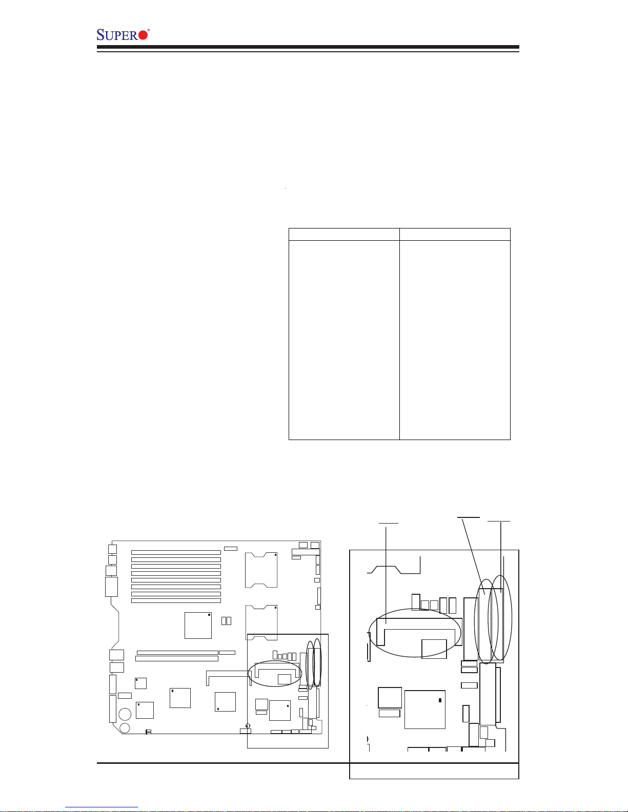
2-28
X6DAR-8G/X6DAR-iG User's Manual
IDE Connectors
There are no jumpers to
configure the onboard IDE#1
and #2 connectors (at J5
and J6, respectively). See
the table on the right for pin
definitions.
Pin Number Function
1 Reset IDE
3 Host Data 7
5 Host Data 6
7 Host Data 5
9 Host Data 4
11 Host Data 3
13 Host Data 2
15 Host Data 1
17 Host Data 0
19 GND
21 DRQ3
23 I/O Write 25 I/O Read 27 IOCHRDY
29 DACK3 31 IRQ14
33 Addr 1
35 Addr 0
37 Chip Select 0
39 Acti vity
Pin Number Function
2 GND
4 Host Data 8
6 Host Data 9
8 Host Data 10
10 Host Data 11
12 Host Data 12
14 Host Data 13
16 Host Data 14
18 Host Data 15
20 Key
22 GND
24 GND
26 GND
28 BALE
30 GND
32 IOCS16 34 GND
36 Addr 2
38 Chip Select 1 40 GND
IDE Connector Pin Definitions
(J5, J6)
IPMI
J9 is designated as the IPMI
Socket for the Motherboard.
K
B
DIMM 4B
Mouse
USB
0/1
J14
C
O
M
1
DIMM 4A
DIMM 3B
DIMM 3A
DIMM 2B
DIMM 2A
DIMM 1B
DIMM 1A
G
L
A
N
1
G
L
A
N
2
VGA
S
C
S
I C
h
B
B
a
tte
ry
JP
G
1
(V
G
A
E
n
a
b
le
)
JP
L
1
(L
A
N
E
n
a
b
le
)
R
A
G
E
-
X
G
L
A
N
C
T
R
L
P
X
H
V
G
A
C
T
R
L
P
C
I-E
x1
6
P
C
I-X
1
3
3
M
H
z
E
7
5
25
(T
u
m
w
a
te
r)
N
o
rth
B
rid
g
e
IC
H
5
R
(S
o
u
th
B
rid
g
e
)
Z
C
R
IPMI 2.0
BIOS
S I/O
7902
SCSI
CTRL
IDE #1
IDE #2
Floppy
SCSI Ch A
WOL
COM2
SCSI
Enable
USB2/3
JD2
JP9
CLR CMOS
Force PW-On
WOR
SPK
SW
SCSI
Ter. A
JPA1
JBT1
S
M
B
FAN5
S
A
T
A
1
SATA0
F
P
C
T
R
L
J
F
1
FAN2
FAN1
20-PinPW
8-Pin
CPU
4-Pin
PW
PW SMB
PW
LED
Chas
Intru.
JL1
JWD
WD
CPU1
CPU2
JPA3
JPA2
S
C
S
I T
e
r. B
OH
J33
J34
J16
J7
J14
JD1
JA1
J5
J6
J12
F
A
N
4
J1B1
J1D1
J38
J32
J4
F
4
J4
F
5
M
e
m
o
ry
S
p
e
e
d
(*N
o
te
:4
)
J11
PW
Fail
S
P
K
R
P
C
I-E
x4
JOH1
JW
O
R
JPF
JS
1
JS
2
JP
1
0
3RDPWDetect
Alarm
Reset
JP
1
1
F
A
N
3
IPMI 2.0
BIOS
S I/O
7902
SCSI
CTRL
IDE #1
IDE #2
Floppy
SCSI Ch A
C
O
M
2
Force PW-On
WOR
SCSI
Ter. A
JPA1
SM
B
FAN5
S
A
TA
1
SATA0
Chas
Intru.
JPA3
JPA2
SCSI Ter. B
JA1
J5
J6
J12
FAN4
J11
JWOR
JPF
JS1
JS2
FAN3
IPMI
IDE1
IDE2
Page 49
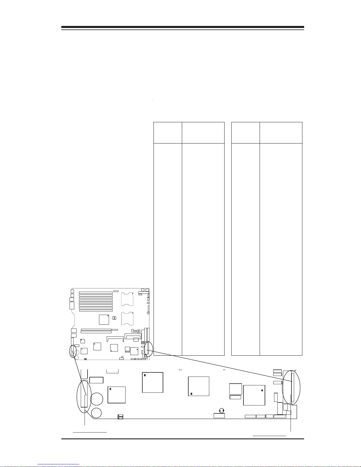
Chapter 2: Installation
2-29
Signal Names
+DB(12)
+DB(13)
+DB(14)
+DB(15)
+DB(P1)
+DB(0)
+DB(1)
+DB(2)
+DB(3)
+DB(4)
+DB(5)
+DB(6)
+DB(7)
+DB(P)
GROUND
DIFFSENS
TERMPWR
TERMPWR
RESERVED
GROUND
+ATN
GROUND
+BSY
+ACK
+RST
+MSG
+SEL
+C/D
+REQ
+I/O
+DB(8)
+DB(9)
+DB(10)
+DB(11)
Connector
Contact
Number
1
2
3
4
5
6
7
8
9
10
11
12
13
14
15
16
17
18
19
20
21
22
23
24
25
26
27
28
29
30
31
32
33
34
Signal Names
-DB(12)
-DB(13)
-DB(14)
-DB(15)
-DB(P1)
-DB(0)
-DB(1)
-DB(2)
-DB(3)
-DB(4)
-DB(5)
-DB(6)
-DB(7)
-DB(P)
GROUND
GROUND
TERMPWR
TERMPWR
RESERVED
GROUND
-ATN
GROUND
-BSY
-ACK
-RST
-MSG
-SEL
-C/D
-REQ
-I/O
-DB(8)
-DB(9)
-DB(10)
-DB(11)
Connector
Contact
Number
35
36
37
38
39
40
41
42
43
44
45
46
47
48
49
50
51
52
53
54
55
56
57
58
59
60
61
62
63
64
65
66
67
68
68-pin Ultra320 SCSI Connectors (JA1 and JA2)
Ultra320 SCSI Connectors
(*X6DAR-8G Only)
Refer to the table below for the pin
definitions of the Ultra320 SCSI
connectors located at JA1 and JA2.
K
B
DIMM 4B
M
o
u
s
e
U
S
B
0
/
1
J14
COM
1
DIMM 4A
DIMM 3B
DIMM 3A
DIMM 2B
DIMM 2A
DIMM 1B
DIMM 1A
G
L
A
N
1
G
L
A
N
2
VGA
S
C
S
I
C
h
B
B
a
t
t
e
r
y
J
P
G
1
(
V
G
A
E
n
a
b
le
)
J
P
L
1
(
L
A
N
E
n
a
b
l
e
)
R
A
G
E
-
X
G
L
A
N
C
T
R
L
P
X
H
V
G
A
C
T
R
L
P
C
I
-
E
x
1
6
P
C
I
-
X
1
3
3
M
H
z
E
7
5
2
5
(
T
u
m
w
a
t
e
r
)
N
o
r
t
h
B
r
i
d
g
e
I
C
H
5
R
(
S
o
u
t
h
B
r
id
g
e
)
Z
C
R
IPMI 2.0
BIOS
S I/O
7902
SCSI
CTRL
IDE #1
IDE #2
Floppy
SCSI Ch A
WOL
C
O
M
2
SCSI
Enable
USB2/3
JD2
JP9
CLR CMOS
Force PW-On
WOR
SPK
SW
S
C
S
I
T
e
r. A
JPA1
JBT1
S
M
B
FAN5
S
A
T
A
1
S
A
T
A
0
F
P
C
T
R
L
JF
1
FAN2
FAN1
20-PinPW
8-Pin
CPU
4-Pin
PW
PW SMB
PW
LED
Chas
Intru.
JL1
JWD
WD
CPU1
CPU2
JPA3
JPA2
S
C
S
I T
e
r. B
OH
J33
J34
J16
J
7
J
1
4
JD1
JA1
J5
J6
J12
FAN4
J1B1
J1D1
J38
J32
J4
F
4
J
4
F
5
M
e
m
o
ry
S
p
e
e
d
(*N
o
te
:4
)
J
1
1
PW
Fail
S
P
K
R
P
C
I
-
E
x
4
JOH1
JWOR
JPF
J
S
1
J
S
2
JP
1
0
3RDPWDetect
Alarm
Reset
JP
1
1
F
A
N
3
V
SCSI Ch B
Battery
JPG1(VGA Enable)
JPL1(LAN Enable)
RAGEX
CTRL
PXH
VGA
CTRL
ICH5R
(South
Bridge)
BIOS
7902
SCSI
CTRL
SCSI Ch A
WOL
COM2
SCSI
Enable
USB2/3
JD2
CLR CMOS
Force PW-On
WOR
SPK
SW
SCSI
Ter. A
JPA1
JBT1
PW
LED
Chas
Intru.
JL1
JWD
WD
JPA3
JPA2
SC
SI Ter. B
OH
J7
J14
JD1
JA1
SPKR
JOH1
JW
O
R
JPF
FAN3
SCSI Ch. A
SCSI Ch. B
Page 50

2-30
X6DAR-8G/X6DAR-iG User's Manual
(*Note: For software installation instructions, please refer to Appendix C. For Adaptec's SCSI SATA HostRAID Utility, please refer
to the CDs that came with your motherboard.)
Page 51

3-1
Chapter 3: Troubleshooting
Chapter 3
Troubleshooting
3-1 Troubleshooting Procedures
Use the following procedures to troubleshoot your system. If you have
followed all of the procedures below and still need assistance, refer to the
‘Technical Support Procedures’ and/or ‘Returning Merchandise for Service’
section(s) in this chapter.
Note: Always disconnect the power cord before adding, changing
or installing any hardware components.
Before Power On
1. Make sure no short circuits exist between the motherboard and chassis.
2. Disconnect all ribbon/wire cables from the motherboard, including those
for the keyboard and mouse.
3. Remove all add-on cards.
4. Install one CPU (making sure it is fully seated) and connect the chassis
speaker and the power LED to the motherboard. (Check all jumper
settings as well.)
5. Use only the correct type of onboard CMOS battery as recommended by
the Manufacturer. Do not install the onboard battery upside down to
avoid possible explosion.
No Power
1. Make sure no short circuits exist between the motherboard and the chassis.
2. Verify that all jumpers are set to their default positions.
3. Check that the 115V/230V switch on the power supply is properly set.
4. Turn the power switch on and off to test the system.
5. The battery on your motherboard may be old. Check to verify that it still
supplies ~3VDC. If it does not, replace it with a new one.
No Video
1. If the power is on but you have no video, remove all the add-on cards
and cables.
2. Use the speaker to determine if any beep codes exist. Refer to the
Appendix for details on beep codes.
Page 52

3-2
X6DAR-8G/X6DAR-iG User's Manual
Losing the System’s Setup Configuration
1. Ensure that you are using a high quality power supply. A poor quality
power supply may cause the system to lose the CMOS setup information. Refer to Section 1-6 for details on recommended power supplies.
2. The battery on your motherboard may be old. Check to verify that it still
supplies ~3VDC. If it does not, replace it with a new one.
3. If the above steps do not fix the Setup Configuration problem, contact
your vendor for repairs.
3-2 Technical Support Procedures
Before contacting Technical Support, please take the following steps. Also,
note that as a motherboard manufacturer, Super Micro does not sell directly
to end-users, so it is best to first check with your distributor or reseller for
troubleshooting services. They should know of any possible problem(s)
with the specific system configuration that was sold to you.
NOTE
If you are a system integrator, VAR or OEM, a POST diagnos-
tics card is recommended. For I/O port 80h codes, refer to
App. B.
Memory Errors
1. Make sure the DIMM modules are properly and fully installed.
2. Determine if different speeds of DIMMs have been installed and verify
that the BIOS setup is configured for the fastest speed of RAM used.
It is recommended to use the same RAM speed for all DIMMs in the
system.
3. Make sure you are using the correct type of ECC Reg. DDR-333/266
(PC2700/2100) SDRAM (*recommended by the manufacturer.)
4. Check for bad DIMM modules or slots by swapping a single module between two slots and noting the results.
5. Make sure all memory modules are fully seated in their slots. As an
interleaved memory scheme is used, you must install two modules at a
time, beginning with Bank 1, then Bank 2, and so on (see Section 2-3).
6. Check the position of the 115V/230V switch on the power supply.
Page 53

3-3
Chapter 3: Troubleshooting
1. Please go through the ‘Troubleshooting Procedures’ and 'Frequently
Asked Question' (FAQ) sections in this chapter or see the FAQs on our
web site (http://www.supermicro.com/support/faqs/) before contacting Technical Support.
2. BIOS upgrades can be downloaded from our web site at
(http://www.supermicro.com/support/bios/).
Note: Not all BIOS can be flashed depending on the modifications
to the boot block code.
3. If you still cannot resolve the problem, include the following infor-
mation when contacting Super Micro for technical support:
• Motherboard model and PCB revision number
• BIOS release date/version (this can be seen on the initial display when
your system first boots up)
•System configuration
An example of a Technical Support form is on our web site at
(http://www.supermicro.com/support/contact.cfm).
4. Distributors: For immediate assistance, please have your account number
ready when placing a call to our technical support department. We can
be reached by e-mail at [email protected], by phone at:
(408) 503-8000, option 2, or by fax at (408)503-8019.
3-3 Frequently Asked Questions
Question: What are the various types of memory that my motherboard can support?
Answer: The X6DAR-8G/X6DAR-iG has eight 184-pin DIMM slots that sup-
port registered ECC DDR-333/266 (PC2700/2100) SDRAM modules. It is
strongly recommended that you do not mix memory modules of different
speeds and sizes.
Question: How do I update my BIOS?
Answer: It is recommended that you do not upgrade your BIOS if you are
experiencing no problems with your system. Updated BIOS files are located
on our web site at http://www.supermicro.com. Please check our BIOS
warning message and the info on how to update your BIOS on our web
site. Also, check the current BIOS revision and make sure it is newer than
your BIOS before downloading. Select your motherboard model and download the BIOS file to your computer. Unzip the BIOS update file and you will
find the readme.txt (flash instructions), the phlash.exe (BIOS flash utility),
the platform.bin (platform file) and the BIOS image (xxxxxx.rom) files. Copy
these files onto a bootable floppy and reboot your system. It is not neces
Page 54

3-4
X6DAR-8G/X6DAR-iG User's Manual
sary to set BIOS boot block protection jumpers on the motherboard. At the
DOS prompt, enter the command "phlash." This will start the flash utility and
give you an opportunity to save your current BIOS image. Flash the boot
block and enter the name of the update BIOS image file.
Question: What's on the CD that came with my motherboard?
Answer: The supplied compact disc has quite a few drivers and programs
that will greatly enhance your system. We recommend that you review the
CD and install the applications you need. Applications on the CD include
chipset drivers for Windows and security and audio drivers.
3-4 Returning Merchandise for Service
A receipt or copy of your invoice marked with the date of purchase is
required before any warranty service will be rendered. You can obtain
service by calling your vendor for a Returned Merchandise Authorization
(RMA) number. When returning to the manufacturer, the RMA number
should be prominently displayed on the outside of the shipping carton, and
mailed prepaid or hand-carried. Shipping and handling charges will be applied for all orders that must be mailed when service is complete.
This warranty only covers normal consumer use and does not cover damages incurred in shipping or from failure due to the alternation, misuse,
abuse or improper maintenance of products.
During the warranty period, contact your distributor first for any product
problems.
Page 55

Chapter 4: BIOS
4-1
Chapter 4
BIOS
4-1 Introduction
This chapter describes the Phoenix BIOS™ Setup utility for the X6DAR-8G/
X6DAR-iG. The Phoenix ROM BIOS is stored in a flash chip and can be
easily upgraded using a floppy disk-based program.
Note: Due to periodic changes to the BIOS, some settings may have been
added or deleted and might not yet be recorded in this manual. Please refer
to the Manual Download area of the Supermicro web site
<http://www.supermicro.com> for any changes to BIOS that may not be
reflected in this manual.
System BIOS
The BIOS is the Basic Input Output System used in all IBM® PC, XT™, AT®,
and PS/2® compatible computers. The Phoenix BIOS flash chip stores the
system parameters, such type of disk drives, video displays, etc. in the
CMOS. The CMOS memory requires very little electrical power. When the
computer is turned off, a back-up battery provides power to the BIOS flash
chip, enabling it to retain system parameters. Each time the computer is
powered-on the computer is configured with the values stored in the BIOS
ROM by the system BIOS, which gains control at boot-up.
How To Change the Configuration Data
The CMOS information that determines the system parameters may be
changed by entering the BIOS Setup utility. This Setup utility can be accessed by pressing the <Delete> key at the appropriate time during system
boot, see below.
Starting the Setup Utility
Normally, the only visible POST (Power On Self Test) routine is the memory
test. As the memory is being tested, press the <Delete> key to enter the
main menu of the BIOS Setup utility. From the main menu, you can access
the other setup screens, such as the Security and Power menus. Beginning with Section 4-3, detailed descriptions are given for each parameter
setting in the Setup utility.
Page 56

4-2
X6DAR-8G/X6DAR-iG User's Manual
4-2 Running Setup
*Default settings are in bold text unless otherwise noted.
The BIOS setup options described in this section are selected by choosing the appropriate text from the main BIOS Setup screen. All displayed
text is described in this section, although the screen display is often all
you need to understand how to set the options (see on next page).
When you first power on the computer, the Phoenix BIOS™ is immediately
activated.
While the BIOS is in control, the Setup program can be activated in one of two
ways:
1. By pressing <Delete> immediately after turning the system on, or
2. When the message shown below appears briefly at the bottom of the
screen during the POST (Power On Self-Test), press the <Delete> key to
activate the main Setup menu:
Press the <Delete> key to enter Setup
4-3 Main BIOS Setup
All main Setup options are described in this section. The main BIOS Setup screen
is displayed below.
Use the Up/Down arrow keys to move among the different settings in each menu.
Use the Left/Right arrow keys to change the options for each setting.
Press the <Esc> key to exit the CMOS Setup Menu. The next section describes
in detail how to navigate through the menus.
Items that use submenus are indicated with the ! icon. With the item highlighted,
press the <Enter> key to access the submenu.
Page 57
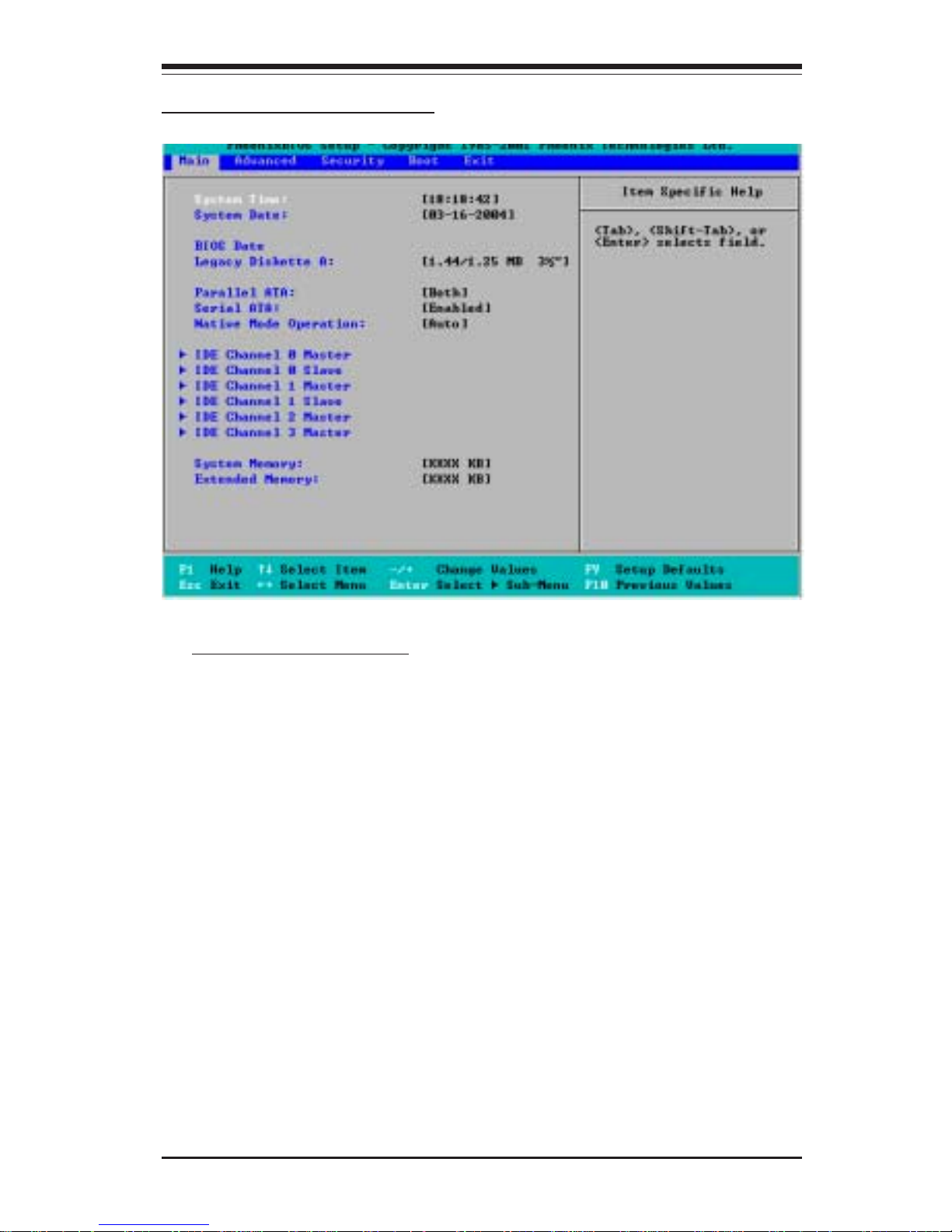
Chapter 4: BIOS
4-3
Main BIOS Setup Menu
Main Setup Features
System Time
To set the system date and time, key in the correct information in the
appropriate fields. Then press the <Enter> key to save the data.
System Date
Using the arrow keys, highlight the month, day and year fields and enter
the correct data. Press the <Enter> key to save the data.
BIOS Date
This feature allows BIOS to automatically display the BIOS date.
Page 58

4-4
X6DAR-8G/X6DAR-iG User's Manual
Legacy Diskette A
This setting allows the user to set the type of floppy disk drive installed as
diskette A. The options are Disabled, 360Kb 5.25 in, 1.2MB 5.25 in, 720Kb
3.5 in, 1.44/1.25MB, 3.5 in and 2.88MB 3.5 in.
Parallel ATA
This setting allows the user to enable or disable the funciton of Parallel
ATA. The options are Disabled, Channel 0, Channel 1 and Both.
Serial ATA
This setting allows the user to enable or disable the funciton of Serial ATA.
The options are Disabled and Enabled.
Serial ATA RAID Feature
Select Enable to enable Serial ATA RAID Functions. (*For the Windows OS
environment, use the RAID driver if this feature is set to "Enabled". If
"Disabled", use the "Non-RAID" driver.)
Native Mode Operation
This option allows the user to select the Native Mode for ATA. Some
Operating Systems are not supported by the Native Mode. The options are:
Serial ATA, Parallel ATA, Auto, and Both.
!!
!!
!IDE Channel 0 Master/Slave, IDE Channel 1 Master/Slave, IDE
Channel 2 Master, IDE Channel 3 Master
These settings allow the user to set the parameters of IDE Channel 0
Master/Slave, IDE Channel 1 Master/Slave, IDE Channel 2 Master, IDE
Channel 3 Master slots. Hit <Enter> to activate the following sub-menu
screen for detailed options of these items. Set the correct configurations
accordingly. The items included in the sub-menu are:
Page 59
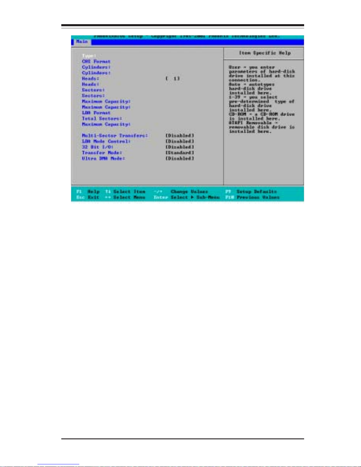
Chapter 4: BIOS
4-5
Type
Selects the type of IDE hard drive. The options are Auto (allows BIOS
to automatically determine the hard drive's capacity, number of heads,
Sectors, Maximum Capacity, LBA Format, ect.). Enter a number from 139 to select a predetermined type of hard drive, CD-ROM and ATAPI
Removable. The option- "User" will allow the user to enter the parameters
of the HDD installed at this connection. The option-"Auto" will allow BIOS
to automatically configure the parameters of the HDD installed at the
connection. Choose the option"1-39" to select a pre-determined HDD
type. Select CD-ROM if a CD-ROM drive is installed. Select ATAPI if a
removable disk drive is installed.
Page 60

4-6
X6DAR-8G/X6DAR-iG User's Manual
Multi-Sector Transfers
Select the number of transfer sectors. The options are Disabled, 2, 4, 6,
8 and 16 Sectors.
LBA Mode Control
This item determines whether Phoenix BIOS will access the IDE Primary
Master Device via LBA mode. The options are Disabled and Enabled.
32 Bit I/O
Selects 32 Bit I/O operation. The options are Enabled and Disabled.
Transfer Mode
Selects the transfer mode. The options are Standard, Fast PIO1, Fast
PIO2, Fast PIO3, Fast PIO4, FPIO3/DMA1 and FPIO4/DMA2.
Ultra DMA Mode
Selects Ultra DMA Mode. The options are Disabled, Mode 0, Mode 1,
Mode 2, Mode 3, Mode 4, Mode 5 and Mode 6.
System Memory
This display informs you how much system memory is recognized as being
present in the system.
Extended Memory
This display informs you how much extended memory is recognized as
being present in the system.
Page 61
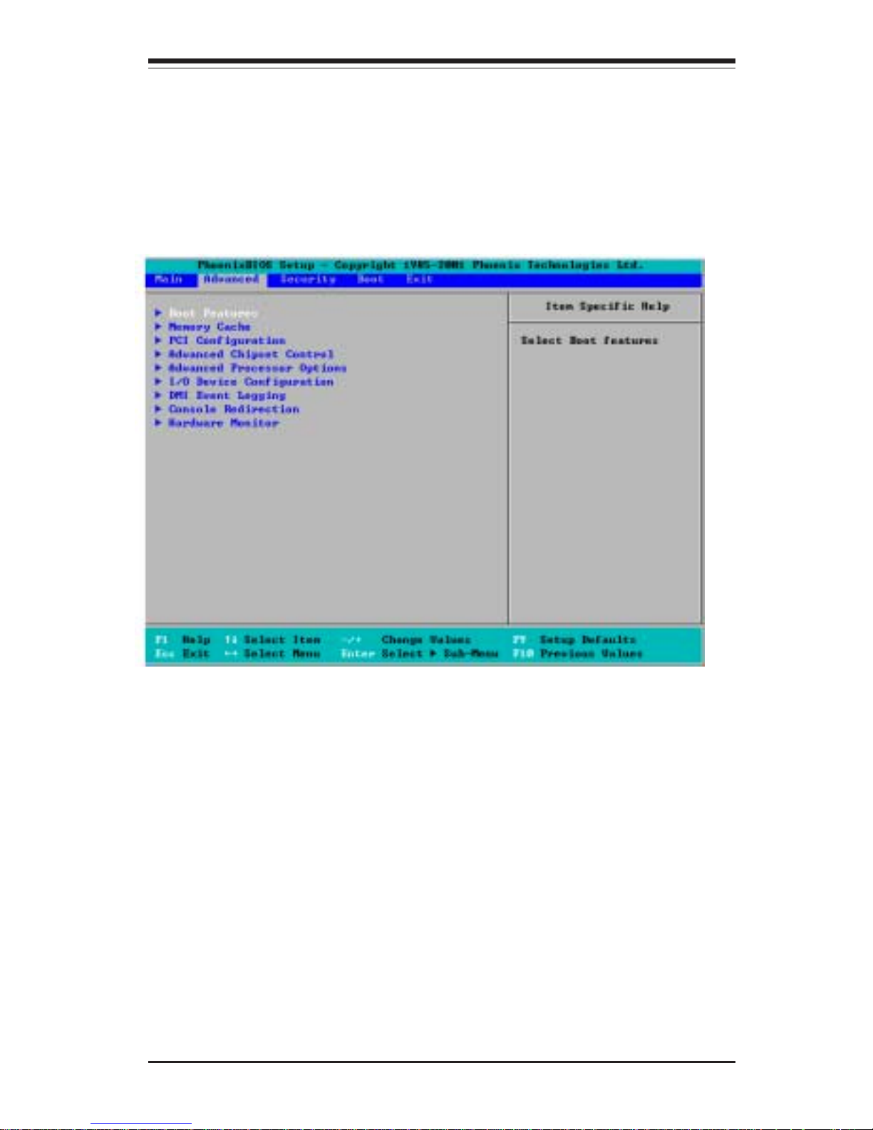
Chapter 4: BIOS
4-7
4-4 Advanced Setup
Choose Advanced from the Phoenix BIOS Setup Utility main menu with the arrow
keys. You should see the following display. The items with a triangle beside
them have sub menus that can be accessed by highlighting the item and pressing
<Enter>. Options for PIR settings are displayed by highlighting the setting option
using the arrow keys and pressing <Enter>. All Advanced BIOS Setup options
are described in this section.
!!
!!
!Boot Features
Access the submenu to make changes to the following settings.
Quick Boot Mode
If enabled, this feature will speed up the POST (Power On Self Test) routine
after the computer is turned on. The settings are Enabled and Disabled. If
Disabled, the POST routine will run at normal speed.
Quiet Boot
This setting allows you to Enable or Disable the diagnostic screen during
boot-up.
Page 62

4-8
X6DAR-8G/X6DAR-iG User's Manual
Summary Screen
This setting allows you to Enable or Disable the summary screen.
ACPI Mode
Use the setting to determine if you want to employ ACPI (Advanced
Configuration and Power Interface) power management on your system.
The options are Yes and No.
Power Button Behavior
This setting allows you to choose how the system powers down upon
pressing the power button. The options are Instant-Off and 4-sec overide.
Keyboard on Now Function
This option alows you to select how the system may be resumed from the
S3-S5 state. The options are Space, or Password.
Power Loss Control
This setting allows you to choose how the system will react when power
returns after an unexpected loss of power. The options are Stay On, Power
Off and Last State.
Watch Dog
This setting is for enabling the Watch Dog feature. The options are Enabled
and Disabled .
!!
!!
!Memory Cache
Cache System BIOS Area
This setting allows you to designate a reserve area in the system
memory to be used as a System BIOS buffer to allow the BIOS write
(cache) its data into this reserved memory area. Select "Write Protect"
to enable this function, and this area will be reserved for BIOS ROM
access only. Select "Uncached" to disable this function and make this
area available for other devices.
Cache Video BIOS Area
This setting allows you to designate a reserve area in the system
memory to be used as a Video BIOS buffer to allow the BIOS write
(cache) its data into this reserved memory area. Select "Write Protect"
to enable the function and this area will be reserved for BIOS ROM
access only. Select "Uncached" to disable this function and make this
area available for other devices.
Page 63

Chapter 4: BIOS
4-9
Cache Base 0-512K
If enabled, this feature will allow the data stored in the base memory
area: block 0-512K to be cached (written) into a buffer, a storage area
in the Static DRM (SDROM) or written into L1, L2, L3 cache inside the
CPU to speed up CPU operations . Select "Uncached" to disable this
funciton. Select "Write Through" to allow data to be cached into the
buffer and written into the system memory at the same time. Select
"Write Protect" to prevent data from being written into the base memory
area of Block 0-512K. Select "Write Back" to allow CPU to write data
back directly from the buffer without writing data to the System Memory
for fast CPU data processing and operation. The options are
"Uncached", "Write Through", "Write Protect", and "Write Back".
Cache Base 512K-640K
If enabled, this feature will allow the data stored in the memory area:
512K-640K to be cached (written) into a buffer, a storage area in the
Static DRM (SDROM) or written into L1, L2, L3 cache inside the CPU to
speed up CPU operations . Select "Uncached" to disable this funciton.
Select "Write Through" to allow data to be cached into the buffer and
written into the system memory at the same time. Select "Write Protect"
to prevent data from being written into the base memory area of Block
0-512K. Select "Write Back" to allow CPU to write data back directly from
the buffer without writing data to the System Memory for fast CPU data
processing and operation. The options are "Uncached", "Write Through",
"Write Protect", and "Write Back".
Cache Extended Memory
If enabled, this feature will allow the data stored in the extended memory
area to be cached (written) into a buffer, a storage area in the Static
DRM (SDROM) or written into L1, L2, L3 cache inside the CPU to speed
up CPU operations . Select "Uncached" to disable this funciton. Select
"Write Through" to allow data to be cached into the buffer and written
into the system memory at the same time. Select "Write Protect" to
prevent data from being written into the base memory area of Block 0512K. Select "Write Back" to allow CPU to write data back directly from
the buffer without writing data to the System Memory for fast CPU data
processing and operation. The options are "Uncached", "Write Through",
"Write Protect", and "Write Back".
Page 64

4-10
X6DAR-8G/X6DAR-iG User's Manual
!!
!!
!PCI Configuration
Access the submenu to make changes to the following settings for PCI
devices.
Onboard GLAN (Gigabit- LAN) OPROM Configure
Enabling this option provides the capability to boot from GLAN. The
options ared Disabled and Enabled.
Onboard SCSI OPROM Configure
Enabling this option provides the caability to boot from SCSI HDD. The
options are Disabled and Enabled.
Reset Configuration Data
If set to Yes, this setting clears the Extended System Configuration Data(ESCD) area. The options are Yes and No.
Frequency for RAID-SLOT/SCSI
This option allows the user to change the bus frequency for the devices
installed in the slot indicated. The options are Auto, PCI 33 MHz, PCI 66
MHz, PCI-X 66 MHz, PCI-X 100 MHz, and PCI-X 133 MHz.
Frequency for PCIX#1/G-LAN
This option allows the user to change the bus frequency of the devices
installed in the slot indicated. The options are Auto, PCI 33 MHz, PCI 66
MHz, PCI-X 66 MHz, PCI-X 100 MHz, and PCI-X 133 MHz.
Page 65

Chapter 4: BIOS
4-11
!!
!!
!PCI-X 133MHz Slot 1/PCI-Exp x4 Slot 2/ PCI-Exp x16 Slot 3
Access the submenu for each of the settings above to make changes to
the following:
Option ROM Scan
When enabled, this setting will initialize the device expansion ROM.
The options are Enabled and Disabled.
Enable Master
This setting allows you to enable the selected device as the PCI bus
master. The options are Enabled and Disabled.
Latency Timer
This setting allows you to set the clock rate for Bus Master.A highprioity, high-throughout device may benefit from a greater Clock rate.
The options are Default, 0020h, 0040h, 0060h, 0080h, 00A0h, 00C0h,
and 00E0h. For Unix, Novell and other Operating Systems, please
select the option:"other". If a drive fails after the installation of a new
software , you might want to change this settiing and try again.
Different OS requires different Bus Master clock rate.
Large Disk Access Mode
This setting determines how large hard drives are to be accessed. The
options are DOS or Other (for Unix, Novellle NetWare and other operating
systems).
!!
!!
!Advanced Chipset Control
Access the submenu to make changes to the following settings.
Force Compliance Mode Entry
This feature allows you to enable the PCI-Express Compliance 1.0 Mode.
The options are: Disabled or Enabled.
Page 66

4-12
X6DAR-8G/X6DAR-iG User's Manual
DRAM Data Integrity Mode
If enabled, this feature allows the data stored in the DRMA memory to
be integrated for faster data processing. The options are 72-bit ECC,
144-bit ECC, Auto, Algorithms and Disabled.
ECC Error Type
This setting lets you select which type of interrupt to be activated as a
result of an ECC error. The options are None, NMI (Non-Maskable
Interrupt), SMI (System Management Interrupt) and SCI (System Control
Interrupt.)
SERR Signal Condition
This setting specifies the conditions required to be qualified as an ECC
error. The options are None, Single Bit, Multiple Bit and Both.
USB Function
This setting allows you to Enable or Disable all functions for the USB
devices specified.
Legacy USB Support
This setting allows you to enable support for Legacy USB devices. The
settings are Enabled and Disabled.
Clock Spectrum Feature
If "Enabled", BIOS will monitor the level of Electromagnetic Interference
caused by the components and will attempt to decrease the interference
whenever needed. The options are Enabled and Disabled.
Memory RAS Feature Control
Select this option to enable the Memory RAS Feature Control The options
are Standard , Mirroring, and Sparing.
Page 67

Chapter 4: BIOS
4-13
!!
!!
!Advanced Processor Options
Access the submenu to make changes to the following settings.
CPU Speed
This is a display that indicates the speed of the installed processor.
Hyper-threading
This setting allows you to Enable or Disable the function of hyperthreading. Enabling hyper-threading results in increased CPU
performance. (Applicable for the XP systems.)
Machine Checking
This setting allows you to Enable or Disable Machine Checking. If
"Enabled", the OS will debug the system during system reset after a
system crash.
Adjacent Cache Line Prefetch
The CPU fetches the cache line for 64 bytes if Disabled. The CPU fetches
both cache lines for 128 bytes as comprised if Enabled.
!!
!!
!I/O Device Configuration
Access the submenu to make changes to the following settings.
KBC Clock input
This setting allows you to set the clock frequency for the Keyboard
Clock. The options are 6MHz, 8MHz, and 12 MHz.
Page 68

4-14
X6DAR-8G/X6DAR-iG User's Manual
On-board COM 1
This setting allows you to assign control of serial port A. The options
are Enabled (user defined), Disabled and Auto (BIOS controlled).
Base I/O Address
Select the base I/O address for serial port A. The options are 3F8,
2F8, 3E8 and 2E8.
Interrupt
Select the IRQ (interrupt request) for serial port A. The options are
IRQ3 and IRQ4.
On-board COM 2
This setting allows you to assign control of serial port B. The options
are Enabled (user defined), Disabled and Auto (BIOS controlled).
Mode
Specify the type of device that will be connected to serial port B. The
options are Normal, IR (for an infrared device) and ASK-IR.
Base I/O Address
Select the base I/O address for serial port B. The options are 3F8,
2F8, 3E8 and 2E8.
Interrupt
Select the IRQ (interrupt request) for serial port B. The options are
IRQ3 and IRQ4.
Page 69

Chapter 4: BIOS
4-15
Parallel Port
This setting allows you to assign control of the parallel port. The options
are Enabled (user defined), Disabled and Auto (BIOS controlled).
Base I/O Address
Select the base I/O address for the parallel port. The options are 378,
278 and 3BC.
Interrupt
Select the IRQ (interrupt request) for the parallel port. The options
are IRQ5 and IRQ7.
Mode
Specify the parallel port mode. The options are Output Only, Bidirectional, EPP and ECP.
DMA Channel
Specify the DMA channel. The options are DMA1 and DMA3.
Floppy Disk Controller
This setting allows you to assign control of the floppy disk controller.
The options are Enabled (user defined), Disabled and Auto (BIOS
controlled).
Base I/O Address
Select the base I/O address for the parallel port. The options are
Primary and Secondary.
Page 70

4-16
X6DAR-8G/X6DAR-iG User's Manual
!!
!!
!DMI Event Logging
Access the submenu to make changes to the following settings.
Event Log Validity
This is a display, not a setting, informing you of the event log validity.
Event Log Capacity
This is a display, not a setting, informing you of the event log capacity.
View DMI Event Log
Highlight this item and press <Enter> to view the contents of the event
log.
Event Logging
This setting allows you to Enable or Disable event logging.
ECC Event Logging
This setting allows you to Enable or Disable ECC event logging.
Mark DMI Events as Read
Highlight this item and press <Enter> to mark the DMI events as read.
Clear All DMI Event Logs
Select Yes and press <Enter> to clear all DMI event logs. The default
setting is "No."
Page 71

Chapter 4: BIOS
4-17
BAUD Rate
Select the BAUD rate for console redirection. The options are 300, 1200,
2400, 9600, 19.2K, 38.4K, 57.6K and 115.2K.
Console Type
Choose from the available options to select the console type for console
redirection. The options are VT100, VT100,8bit, PC-ANSI, 7bit, PC-ANSI,
VT100+, VT-UTF8.
Flow Control
Choose from the available options to select the flow control for console
redirection. The options are: None, XON/XOFF, and CTS/RTS.
Console Connection
Select the console connection: either Direct or Via Modem.
Continue CR after POST
Choose whether to continue with console redirection after the POST
routine. The options are On and Off.
!!
!!
!Console Redirection
Access the submenu to make changes to the following settings.
COM Port Address
Specifies to redirect the console to On-board COM A or On-board COM
B. This setting can also be Disabled.
Page 72

4-18
X6DAR-8G/X6DAR-iG User's Manual
!!
!!
!Hardware Monitor Logic
CPU Temperature Threshold
This option allows the user to set a CPU temperature threshold that
will activate the alarm system when the CPU temperature reaches this
pre-set temperature threshold. The options are 85oC, 90oC, 95oC and
100oC.
Highlight this and hit <Enter> to see monitor data for the following items:
CPU1 Temperature: This item displays CPU1 Temperature.
CPU2 Temperature: This item displays CPU2 Temperature.
System Temperature: This item displays the system Temperature.
Fan Speed Control Modules:
This feature allows the user to decide how the system controls the speeds
of the onboard fans. If the option is set to "3-pin Server", the fan speed is
controlled by the CPU temperature. When the CPU temperature is higher,
the fan speed will be higher as well. If set to "Disable," the fan speed
control is disabled and the onboard fan will run at the full speed (12V) at
all time. The Options are: "Disable" and "3-pin Server."
Fan1 Speed to Fan5 Speed
Page 73

Chapter 4: BIOS
4-19
Vcore A
Vcore B
P3V3
P5V
N12V
P12V
VDD
P5Vsb
Page 74
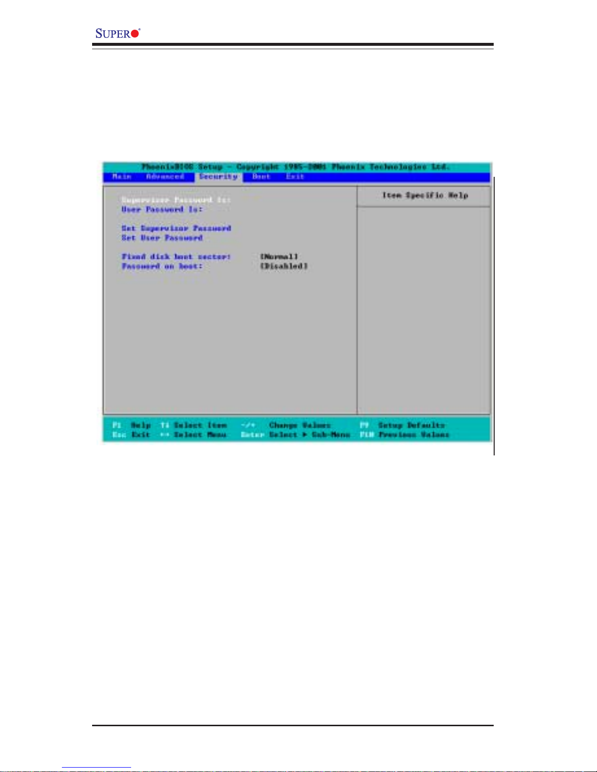
4-20
X6DAR-8G/X6DAR-iG User's Manual
4-5 Security
Choose Security from the Phoenix BIOS Setup Utility main menu with the arrow
keys. You should see the following display. Security setting options are
displayed by highlighting the setting using the arrow keys and pressing <Enter>.
All Security BIOS settings are described in this section.
Supervisor Password Is:
This displays whether a supervisor password has been entered for the
system. Clear means such a password has not been used and Set means
a supervisor password has been entered for the system.
User Password Is:
This displays whether a user password has been entered for the system.
Clear means such a password has not been used and Set means a user
password has been entered for the system.
Page 75

Chapter 4: BIOS
4-21
Set Supervisor Password
When the item "Set Supervisor Password" is highlighted, hit the <Enter> key.
When prompted, type the Supervisor's password in the dialogue box to set
or to change supervisor's password, which allows access to BIOS.
Set User Password
When the item "Set User Password" is highlighted, hit the <Enter> key.
When prompted, type the user's password in the dialogue box to set or to
change the user's password, which allows access to the system at bootup.
Fixed Disk Boot Sector
This setting may offer some protection against viruses when set to Write
Protect, which protects the boot sector on the hard drive from having a
virus written to it. The other option is Normal.
Password on Boot
This setting allows you to require a password to be entered when the
system boots up. The options are Enabled (password required) and
Disabled (password not required).
Page 76
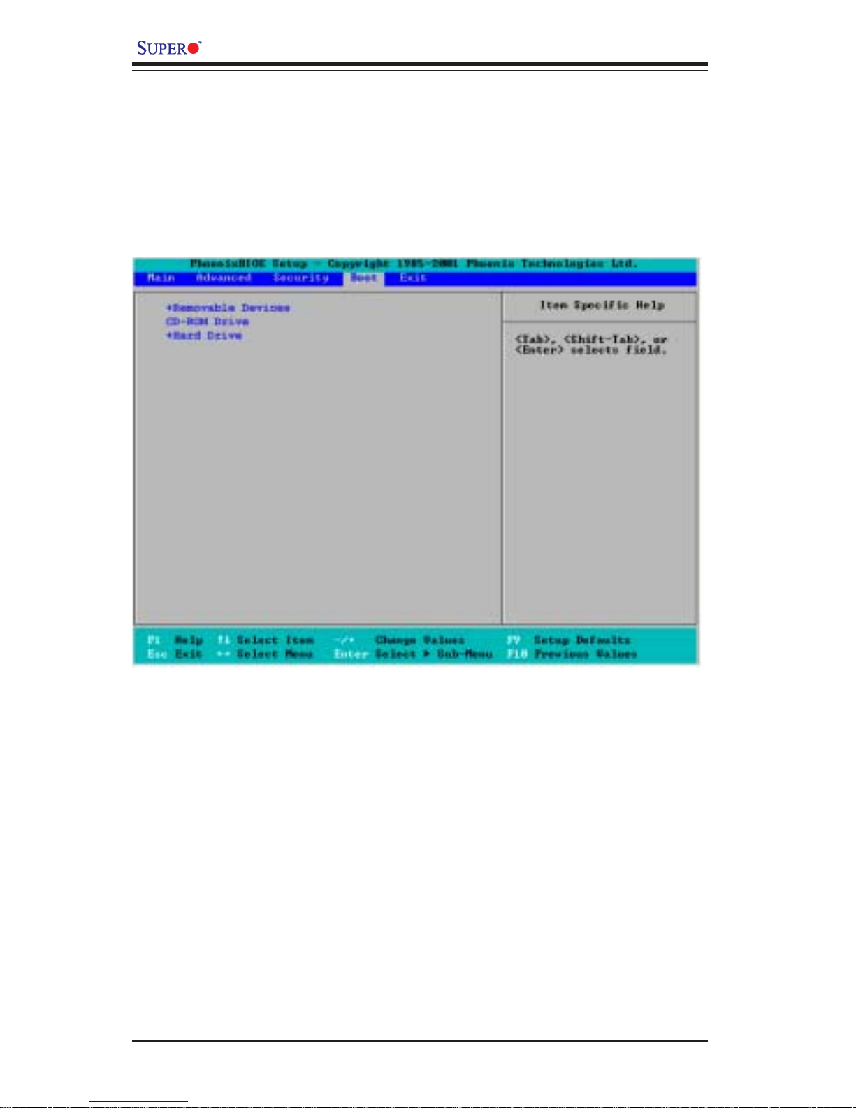
4-22
X6DAR-8G/X6DAR-iG User's Manual
4-6 Boot
Choose Boot from the Phoenix BIOS Setup Utility main menu with the arrow keys.
You should see the following display. Highlighting a setting with a + or - will
expand or collapse that entry. See details on how to change the order and specs
of boot devices in the Item Specific Help window. All Boot BIOS settings are
described in this section.
+Removable Devices
Highlight and press <Enter> to expand the field. See details on how to
change the order and specs of devices in the Item Specific Help window.
CD-ROM Drive
See details on how to change the order and specs of the CD-ROM drive in
the Item Specific Help window.
+Hard Drive
Highlight and press <Enter> to expand the field. See details on how to
change the order and specs of hard drives in the Item Specific Help
window.
Page 77
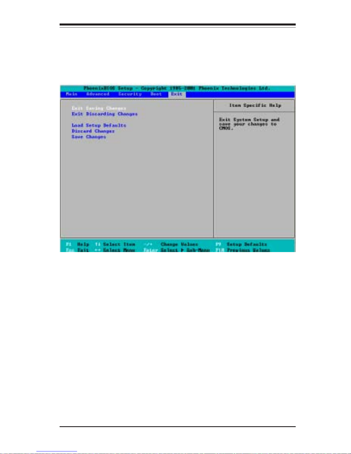
Chapter 4: BIOS
4-23
4-7 Exit
Choose Exit from the Phoenix BIOS Setup Utility main menu with the arrow keys.
You should see the following display. All Exit BIOS settings are described in this
section.
Exit Saving Changes
Highlight this item and hit <Enter> to save any changes you made and to
exit the BIOS Setup utility.
Exit Discarding Changes
Highlight this item and hit <Enter> to exit the BIOS Setup utility without saving
any changes you may have made.
Load Setup Defaults
Highlight this item and hit <Enter> to load the default settings for all items in
the BIOS Setup. These are the safest settings to use.
Page 78

4-24
X6DAR-8G/X6DAR-iG User's Manual
Discard Changes
Highlight this item and hit <Enter> to discard (cancel) any changes you
made. You will remain in the Setup utility.
Save Changes
Highlight this item and hit <Enter> to save any changes you made. You will
remain in the Setup utility.
Page 79

A-1
Appendix A: BIOS POST Messages
Appendix A
BIOS POST Messages
During the Power-On Self-Test (POST), the BIOS will check for problems. If a problem
is found, the BIOS will activate an alarm or display a message. The following is a list
of such BIOS messages.
Failure Fixed Disk
Fixed disk is not working or not configured properly. Check to see if fixed disk is
attached properly. Run Setup. Find out if the fixed-disk type is correctly identified.
Stuck key
Stuck key on keyboard.
Keyboard error
Keyboard not working.
Keyboard Controller Failed
Keyboard controller failed test. May require replacing keyboard controller.
Keyboard locked - Unlock key switch
Unlock the system to proceed.
Monitor type does not match CMOS - Run SETUP
Monitor type not correctly identified in Setup
Shadow Ram Failed at offset: nnnn
Shadow RAM failed at offset nnnn of the 64k block at which the error
was detected.
System RAM Failed at offset: nnnn
System RAM failed at offset nnnn of in the 64k block at which the error
was detected.
Extended RAM Failed at offset: nnnn Extended memory not
working or not configured properly at offset nnnn.
System battery is dead - Replace and run SETUP
The CMOS clock battery indicator shows the battery is dead. Replace the
battery and run Setup to reconfigure the system.
Page 80

A-2
X6DAR-8G/X6DAR-iG User's Manual
System CMOS checksum bad - Default configuration used
System CMOS has been corrupted or modified incorrectly, perhaps by an
application program that changes data stored in CMOS. The BIOS installed Default
Setup Values. If you do not want these values, enter Setup and enter your own
values. If the error persists, check the system battery or contact your dealer.
System timer error
The timer test failed. Requires repair of system board.
Real time clock error
Real-Time Clock fails BIOS hardware test. May require board repair.
Check date and time settings
BIOS found date or time out of range and reset the Real-Time Clock. May require
setting legal date (1991-2099).
Previous boot incomplete - Default configuration used
Previous POST did not complete successfully. POST loads default values and
offers to run Setup. If the failure was caused by incorrect values and they are
not corrected, the next boot will likely fail. On systems with control of wait
states, improper Setup settings can also terminate POST and cause this error on
the next boot. Run Setup and verify that the waitstate configuration is correct.
This error is cleared the next time the system is booted.
Memory Size found by POST differed from CMOS
Memory size found by POST differed from CMOS.
Diskette drive A error
Diskette drive B error
Drive A: or B: is present but fails the BIOS POST diskette tests. Check to see that
the drive is defined with the proper diskette type in Setup and that the diskette
drive is attached correctly.
Incorrect Drive A type - run SETUP
Type of floppy drive A: not correctly identified in Setup.
Incorrect Drive B type - run SETUP
Type of floppy drive B: not correctly identified in Setup.
Page 81

A-3
Appendix A: BIOS POST Messages
System cache error - Cache disabled
RAM cache failed and BIOS disabled the cache. On older boards, check the
cache jumpers. You may have to replace the cache. See your dealer. A disabled
cache slows system performance considerably.
CPU ID:
CPU socket number for Multi-Processor error.
EISA CMOS not writeable
ServerBIOS2 test error: Cannot write to EISA CMOS.
DMA Test Failed
ServerBIOS2 test error: Cannot write to extended DMA (Direct Memory
Access) registers.
Software NMI Failed
ServerBIOS2 test error: Cannot generate software NMI (Non-Maskable
Interrupt).
Fail-Safe Timer NMI Failed
ServerBIOS2 test error: Fail-Safe Timer takes too long.
device Address Conflict
Address conflict for specified device.
Allocation Error for: device
Run ISA or EISA Configuration Utility to resolve resource conflict for the
specified device.
CD ROM Drive
CD ROM Drive identified.
Entering SETUP ...
Starting Setup program
Failing Bits: nnnn
The hex number nnnn is a map of the bits at the RAM address which failed
the memory test. Each 1 (one) in the map indicates a failed bit. See errors
230, 231, or 232 above for offset address of the failure in System,
Extended, or Shadow memory.
Page 82

A-4
X6DAR-8G/X6DAR-iG User's Manual
Fixed Disk n
Fixed disk n (0-3) identified.
Invalid System Configuration Data
Problem with NVRAM (CMOS) data.
I/O device IRQ conflict
I/O device IRQ conflict error.
PS/2 Mouse Boot Summary Screen:
PS/2 Mouse installed.
nnnn kB Extended RAM Passed
Where nnnn is the amount of RAM in kilobytes successfully tested.
nnnn Cache SRAM Passed
Where nnnn is the amount of system cache in kilobytes successfully tested.
nnnn kB Shadow RAM Passed
Where nnnn is the amount of shadow RAM in kilobytes successfully
tested.
nnnn kB System RAM Passed
Where nnnn is the amount of system RAM in kilobytes successfully tested.
One or more I2O Block Storage Devices were excluded from the Setup
Boot Menu
There was not enough room in the IPL table to display all installed I2O blockstorage devices.
Operating system not found
Operating system cannot be located on either drive A: or drive C:. Enter Setup
and see if fixed disk and drive A: are properly identified.
Parity Check 1 nnnn
Parity error found in the system bus. BIOS attempts to locate the address and
display it on the screen. If it cannot locate the address, it displays ????. Parity is
a method for checking errors in binary data. A parity error indicates that some
data has been corrupted.
Page 83

A-5
Appendix A: BIOS POST Messages
Parity Check 2 nnnn
Parity error found in the I/O bus. BIOS attempts to locate the address and display
it on the screen. If it cannot locate the address, it displays ????.
Press <F1> to resume, <F2> to Setup, <F3> for previous
Displayed after any recoverable error message. Press <F1> to start the boot
process or <F2> to enter Setup and change the settings. Press <F3> to display
the previous screen (usually an initialization error of an Option ROM, i.e., an
add-on card). Write down and follow the information shown on the screen.
Press <F2> to enter Setup
Optional message displayed during POST. Can be turned off in Setup.
PS/2 Mouse:
PS/2 mouse identified.
Run the I2O Configuration Utility
One or more unclaimed block storage devices have the Configuration Request bit
set in the LCT. Run an I2O Configuration Utility (e.g. the SAC utility).
System BIOS shadowed
System BIOS copied to shadow RAM.
UMB upper limit segment address: nnnn
Displays the address nnnn of the upper limit of Upper Memory Blocks,
indicating released segments of the BIOS which can be reclaimed by a virtual
memory manager.
Video BIOS shadowed
Video BIOS successfully copied to shadow RAM.
Page 84

A-6
X6DAR-8G/X6DAR-iG User's Manual
Notes
Page 85

Appendix B: BIOS POST Codes
B-1
This section lists the POST (Power On Self Test) codes for the PhoenixBIOS. POST
codes are divided into two categories: recoverable and terminal.
Recoverable POST Errors
When a recoverable type of error occurs during POST, the BIOS will display
an POST code that describes the problem. BIOS may also issue one of the
following beep codes:
1 long and two short beeps - video configuration error
1 continuous long beep - no memory detected
Terminal POST Errors
If a terminal type of error occurs, BIOS will shut down the system. Before
doing so, BIOS will write the error to port 80h, attempt to initialize video and
write the error in the top left corner of the screen.
The following is a list of codes that may be written to port 80h.
Appendix B
BIOS POST Codes
POST Code Description
02h Verify Real Mode
03 h Disable Non-Maskable Interrupt (NMI)
04h Get CPU type
06h Initialize system hardware
07 h Disable shadow and execute code from the ROM.
08 h Initialize chipset with initial POST values
09h Set IN POST flag
0Ah Initialize CPU registers
0Bh Enable CPU cache
0C h Initialize caches to initial POST values
0Eh Initialize I/O component
0Fh Initialize the local bus IDE
10 h Initialize Power Management
11 h Load alternate registers with initial POST values
12 h Restore CPU control word during warm boot
13 h Initialize PCI Bus Mastering devices
14 h Initialize keyboard controller
16 h 1-2-2-3 BIOS ROM checksum
17 h Initialize cache before memory Auto size
Page 86

B-2
X6DAR-8G/X6DAR-iG User's Manual
POST Code Description
18h 8254 timer initialization
1Ah 8237 DMA controller initialization
1Ch Reset Programmable Interrupt Controller
20 h 1-3-1-1 Test DRAM refresh
22 h 1-3-1-3 Test 8742 Keyboard Controller
24 h Set ES segment register to 4 GB
28h Auto size DRAM
29h Initialize POST Memory Manager
2Ah Clear 512 kB base RAM
2Ch 1-3-4-1 RAM failure on address line xxxx*
2Eh 1-3-4-3 RAM failure on data bits xxxx* of low byte of
memory bus
2Fh Enable cache before system BIOS shadow
32 h Test CPU bus-clock frequency
33 h Initialize Phoenix Dispatch Manager
36 h Warm start shut down
38 h Shadow system BIOS ROM
3Ah Auto size cache
3C h Advanced configuration of chipset registers
3D h Load alternate registers with CMOS values
41 h Initialize extended memory for RomPilot
42 h Initialize interrupt vectors
45 h POST device initialization
46 h 2-1-2-3 Check ROM copyright notice
47 h Initialize I20 support
48 h Check video configuration against CMOS
49 h Initialize PCI bus and devices
4Ah Initialize all video adapters in system
4Bh QuietBoot start (optional)
4Ch Shadow video BIOS ROM
4Eh Display BIOS copyright notice
4Fh Initialize MultiBoot
50 h Display CPU type and speed
51h Initialize EISA board
52 h Test keyboard
54h Set key click if enabled
55 h Enable USB devices
58 h 2-2-3-1 Test for unexpected interrupts
59 h Initialize POST display service
5Ah Display prompt “Press F2 to enter SETUP”
5Bh Disable CPU cache
Page 87

Appendix B: BIOS POST Codes
B-3
POST Code Description
5Ch Test RAM between 512 and 640 kB
60 h Test extended memory
62h Test extended memory address lines
64h Jump to UserPatch1
66h Configure advanced cache registers
67 h Initialize Multi Processor APIC
68 h Enable external and CPU caches
69h Setup System Management Mode (SMM) area
6Ah Display external L2 cache size
6Bh Load custom defaults (optional)
6Ch Display shadow-area message
6Eh Display possible high address for UMB recovery
70h Display error messages
72 h Check for configuration errors
76 h Check for keyboard errors
7C h Set up hardware interrupt vectors
7D h Initialize Intelligent System Monitoring
7Eh Initialize coprocessor if present
80 h Disable onboard Super I/O ports and IRQs
81 h Late POST device initialization
82 h Detect and install external RS232 ports
83 h Configure non-MCD IDE controllers
84 h Detect and install external parallel ports
85 h Initialize PC-compatible PnP ISA devices
86 h Re-initialize onboard I/O ports.
87h Configure Motherboard Configurable Devices
(optional)
88h Initialize BIOS Data Area
89 h Enable Non-Maskable Interrupts (NMIs)
8Ah Initialize Extended BIOS Data Area
8Bh Test and initialize PS/2 mouse
8C h Initialize floppy controller
8Fh Determine number of ATA drives (optional)
90h Initialize hard-disk controllers
91h Initialize local-bus hard-disk controllers
92h Jump to UserPatch2
93 h Build MPTABLE for multi-processor boards
95h Install CD ROM for boot
96 h Clear huge ES segment register
97 h Fix up Multi Processor table
98 h 1-2 Search for option ROMs. One long, two short
beeps on checksum failure
Page 88

B-4
X6DAR-8G/X6DAR-iG User's Manual
POST Code Description
99h Check for SMART Drive (optional)
9Ah Shadow option ROMs
9C h Set up Power Management
9D h Initialize security engine (optional)
9Eh Enable hardware interrupts
9Fh Determine number of ATA and SCSI drives
A0h Set time of day
A2h Check key lock
A4h Initialize typematic rate
A8h Erase F2 prompt
AAh Scan for F2 key stroke
ACh Enter SETUP
AEh Clear Boot flag
B0h Check for errors
B1h Inform RomPilot about the end of POST.
B2h POST done - prepare to boot operating system
B4h 1 One short beep before boot
B5h Terminate QuietBoot (optional)
B6h Check password (optional)
B7h Initialize ACPI BIOS
B9h Prepare Boot
BA h Initialize SMBIOS
BBh Initialize PnP Option ROMs
BCh Clear parity checkers
BDh Display MultiBoot menu
BEh Clear screen (optional)
BFh Check virus and backup reminders
C0h Try to boot with INT 19
C1h Initialize POST Error Manager (PEM)
C2 h Initialize error logging
C3 h Initialize error display function
C4 h Initialize system error handler
C5 h PnPnd dual CMOS (optional)
C6 h Initialize note dock (optional)
C7 h Initialize note dock late
C8 h Force check (optional)
C9h Extended checksum (optional)
CAh Redirect Int 15h to enable remote keyboard
CBh Redirect Int 13h to Memory Technologies
Devices such as ROM, RAM, PCMCIA, and
serial disk
CC h Redirect Int 10h to enable remote serial video
Page 89

Appendix B: BIOS POST Codes
B-5
POST Code Description
CDh Re-map I/O and memory for PCMCIA
CEh Initialize digitizer and display message
D2h Unknown interrupt
The following are for boot block in Flash ROM
POST Code Description
E0h Initialize the chipset
E1h Initialize the bridge
E2h Initialize the CPU
E3h Initialize system timer
E4h Initialize system I/O
E5h Check force recovery boot
E6h Checksum BIOS ROM
E7h Go to BIOS
E8h Set Huge Segment
E9h Initialize Multi Processor
EAh Initialize OEM special code
EBh Initialize PIC and DMA
ECh Initialize Memory type
EDh Initialize Memory size
EEh Shadow Boot Block
EFh System memory test
F0h Initialize interrupt vectors
F1h Initialize Run Time Clock
F2h Initialize video
F3h Initialize System Management Manager
F4h Output one beep
F5h Clear Huge Segment
F6h Boot to Mini DOS
F7h Boot to Full DOS
* If the BIOS detects error 2C, 2E, or 30 (base 512K RAM error), it displays an additional
word-bitmap (xxxx) indicating the address line or bits that failed. For example, “2C
0002” means address line 1 (bit one set) has failed. “2E 1020" means data bits 12
and 5 (bits 12 and 5 set) have failed in the lower 16 bits. The BIOS also sends the
bitmap to the port-80 LED display. It first displays the checkpoint code, followed by
a delay, the high-order byte, another delay, and then the loworder byte of the error.
It repeats this sequence continuously.
Page 90

B-6
X6DAR-8G/X6DAR-iG User's Manual
Notes
Page 91

Appendix C: Software Installation Instructions
C-1
Appendix C
Installing Software Drivers and Windows
Operating System
After all the hardware has been installed, you must first configure the
Adaptec Embedded Serial ATA RAID Driver before you install the Windows
operating system. The necessary drivers are all included on the Supermicro
bootable CDs that came packaged with your motherboard. (*For
Adaptec's SCSI HostRAID Utility, please refer to the CDs that came
with your motherboard.)
C-1 Introduction to the Adaptec Embedded Serial ATA
RAID Controller Driver
Serial ATA (SATA)
Serial ATA(SATA) is a physical storage interface. It uses a single cable with
a minimum of four wires to create a point-to-point connection between
devices. It is a serial link which supports SATA Transfer rates from
150MBps. Because the serial cables used in SATA are thinner than the
traditional cables used in Parallel ATA(PATA), SATA systems have better
airflow and can be installed in smaller chassis than Parallel ATA. In addition,
the cables used in PATA can only extend to 40cm long, while Serial ATA
cables can extend up to one meter. Overall, Serial ATA provides better
functionality than Parallel ATA.
Introduction to the Intel ICH5R I/O Controller Hub
Located in the South Bridge of the Intel E7525 (Tumwater) Chipset, the ICH5R
I/O Controller Hub provides the I/O subsystem with access to the rest of the
system. It supports 2-channel Ultra ATA/100 Bus Master IDE controller (PATA)
and two Serial ATA (SATA) Host Controllers, which support up to two Serial
ATA ports and up to two RAID drives.
Page 92

C-2
X6DAR-8G/X6DAR-iG User's Manual
Configuring BIOS settings for the SATA RAID Functions
1. Press the <Del> key during system bootup to enter the BIOS Setup
Utility.
(*Note: If it is the first time to power on the system, we recommend that
you load the Optimized Default Settings. If you have already done so,
please skip to Step 3.
2. Use the arrow keys to select the "Exit" Menu. Once in the "Exit" Menu,
scroll down the menu to select the item- "Load Optimized Default settings"
and press the <Enter> key. Select "OK" to confirm the selection. Press
the <Enter> key to load the default settings to the BIOS.
3. Use the arrow keys to select the "Main" Menu in the BIOS.
4. Scroll down to the next item-"SATA RAID Enable", select "Enabled" and
press <Enter>.
5. Tap the <Esc> key and scroll down to "Exit". Select "Save and Exit"
from the "Exit" menu. Press the <Enter> key to save the changes and exit
the BIOS.
6. Once you've exited the BIOS Utility, the system will re-boot.
7. During the system startup, press the <Ctrl> and the <A> keys simultaneously to run the Adaptec RAID Configuration Utility when prompted by
the following message:
Press <Ctrl><A> for Adaptec RAID Configuration Utility
Page 93

Appendix C: Software Installation Instructions
C-3
The Adaptec Embedded Serial ATA with HostRAID
Controller Driver
Adaptec's Embedded Serial ATA RAID with HostRAID controller adds RAID
functionality to the Serial ATA I/O controller by supporting RAID 0
(Striping) or RAID 1 (Mirroring) to enhance the industry's pioneer PCI-to-e
host controller products. RAID striping (RAID 0) can greatly improve hard
disk I/O performance because of its capability in striping data across
multiple drives. RAID mirroring (RAID 1) allows the data to be simultaneously written to two drives, so critical data is always available even if
a single hard disk fails. Due to the built-in functionality, the X6DAR-8G/
X6DAR-iG is specially designed to keep pace with the increasing
performance demands of computer systems by improving disk I/O
throughput and providing data accessibility regardless of a single disk
failure. By incorporating the Adaptec Embedded Serial ATA into the
motherboard design, Supermicro's X6DAR-8G/X6DAR-iG offers the user
with the benefits of SATARAID without the high costs associated with
hardware RAID applications.
(*Note: For Adaptec's RAID Driver Installation Instructions, please refer to
the Adaptec RAID Controller User's Guide: "Emb_SA_RAID_UG.pdf" in the
CD that came with this motherboard. You can also download a copy of
Adaptec's User's Guide from our web site at www.supermicro.com.)
Using the Adaptec RAID Configuration Utility (ARC)
The Adaptec RAID Configuration Utility is an embedded BIOS Utility,
including:
*Array Configuration Utility: Use this utility when you want to create,
configure and manage arrays.
* Disk Utilities: Use this option to format or verify disks.
To run the Adaptec RAID Configuration Utility, you will need to enable the
RAID function in the system BIOS (refer to Chapter 4 for System BIOS
Configurations), and then, press the <Ctrl> and <A> keys simultaneously
when prompted to do so during the system startup. (Refer to the previous page for detailed instructions.)
(*Note: To select an option, use the arrow keys to highlight the item and
then press the <Enter> key to select it. To return to the previous menu,
press the <ESC> key.)
A. Using the Array Configuration Utility (ACU)
The Array Configuration Utility (ACU) enables you to create, manage, and
delete arrays from the controller’s BIOS, add and delete spare drives, and
initialize drives. During the system startup, press <Ctrl> and <A> key
simultaneously, and the main menu will appear.
Page 94
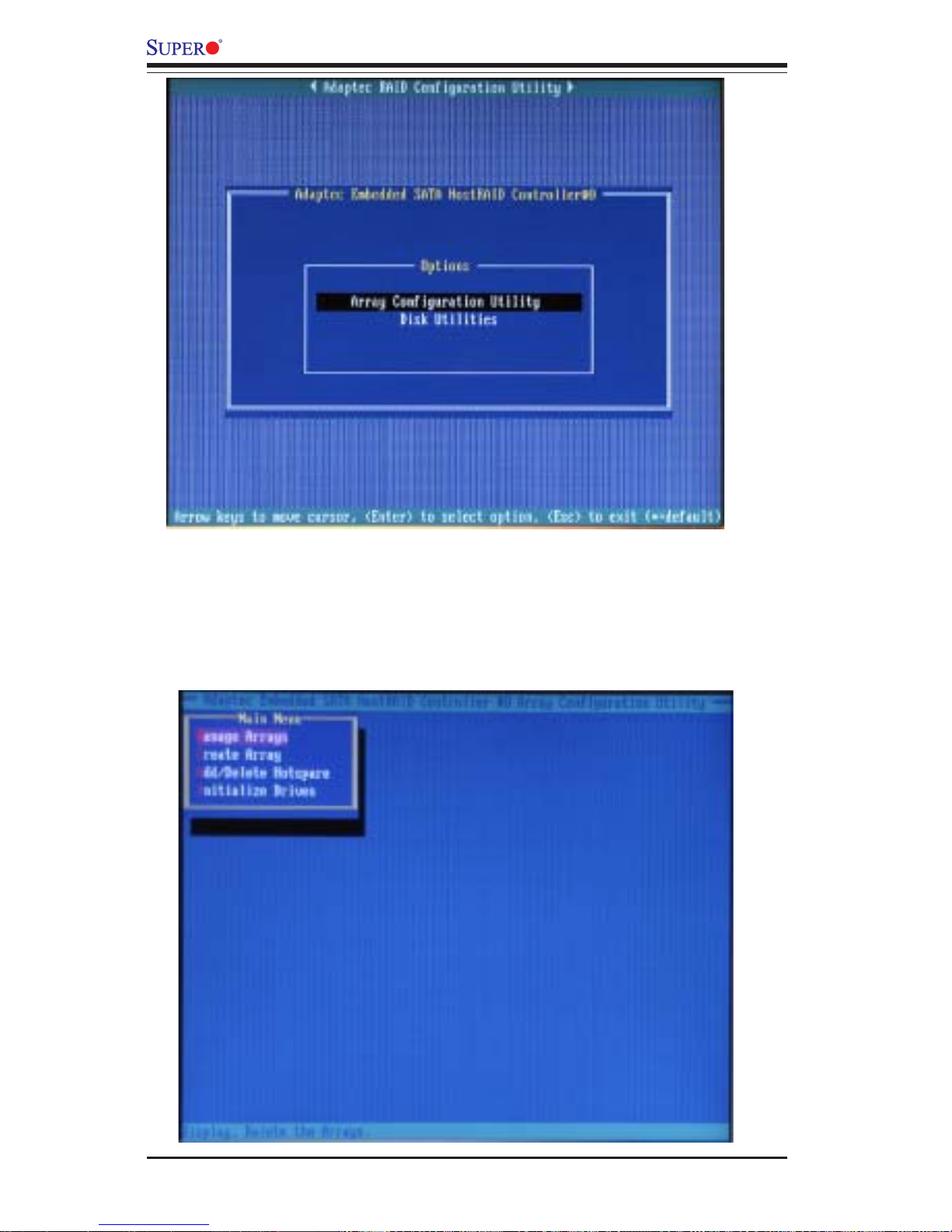
C-4
X6DAR-8G/X6DAR-iG User's Manual
Managing Arrays
Select this option to view array properties, and delete arrays. The
following sections describe the operations Of "Managing Arrays".
To select this option, use the arrow keys and the <enter> key to select
"Managing Arrays" from the main menu (as shown above).
Page 95

Appendix C: Software Installation Instructions
C-5
Viewing Array Properties
To view the properties of an existing array:
1. At the BIOS prompt, press Ctrl+A.
2. From the ARC menu, select Array Configuration Utility (ACU).
3. From the ACU menu, select Manage Arrays (as shown on the
previous screen.)
4. From the List of Arrays dialog box, select the array you want to view
and press Enter.
The Array Properties dialog box appears, showing detailed
information on the array. The physical disks associated with the array are
displayed here.
5. Press Esc to return to the previous menu.
Deleting Arrays
*Warning: Back up the data on an array before you delete it to prevent
the loss of data. Deleted arrays cannot be restored.
To delete an existing array:
1. Turn on your computer and press Ctrl+A when prompted to access
the ARC utility.
2. From the ARC main menu, select Array Configuration Utility
(ACU).
3. From the ACU menu, select Manage Arrays.
4. Select the array you wish to delete and press Delete.
5. In the Array Properties dialog box, select Delete and press
Enter. The following prompt is displayed:
*Warning!! Deleting the array will render array unusable. Do you
want to delete the array?(Yes/No):
RAID 1 only—the following prompt is also displayed:
Deleting the partition will result in data loss! Do you also want to
delete the partition? (Yes/No):
6. Press Yes to delete the array or partition or No to return to the
previous menu.
7. Press Esc to return to the previous menu.
Page 96
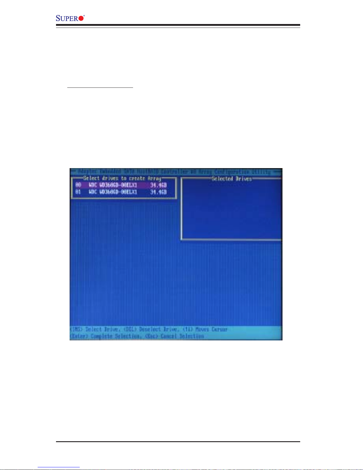
C-6
X6DAR-8G/X6DAR-iG User's Manual
Creating Arrays
Before creating arrays, make sure the disks for the array are
connected and installed in your system. Note that disks with no
usable space, or disks that are un-initialized are shown in gray and
cannot be used. See Initializing Disk Drives.
To create an array:
1 Turn on your computer and press Ctrl+A when prompted to
access the ARC utility.
2 From the ARC menu, select Array Configuration Utility Main Menu
(ACU) (as shown on the first screen on page B-5).
3 From the ACU menu, select Create Array.
4 Select the disks for the new array and press Insert (as the screen
shown below).
(*Note: To deselect any disk, highlight the disk and press Delete.)
5 Press Enter when both disks for the new array are selected. The
Array Properties menu displays (as the screen shown on the next page).
Page 97
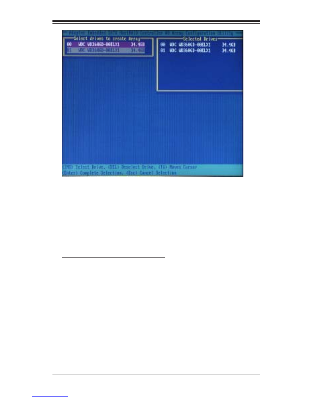
Appendix C: Software Installation Instructions
C-7
Assigning Array Properties
Once you've create a new array, you are ready to assign the properties
to the array.
*Caution: Once the array is created and its properties are assigned,
you cannot change the array properties using the ACU. You will need to
use the Adaptec Storage Manager - Browser Edition. (Refer to Adaptec's
User's Guide in the enclosed CD.)
To assign properties to the new array:
1. In the Array Properties menu (as shown in the following screen),
select an array type and press Enter.
Note that only the available array types: RAID 0, and RAID1, are displayed on the screen. (*RAID 0 or RAID 1 requires two drives.)
Page 98
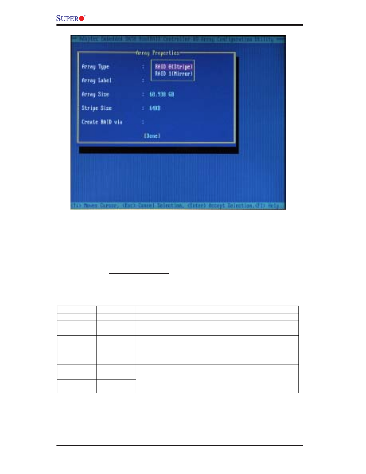
C-8
X6DAR-8G/X6DAR-iG User's Manual
2. Under the item "Arrays Label", type in an label and press Enter.
(*Note: The label shall not be more than 15 characters.)
3. For RAID 0, select the desired stripe size. (*Note: Available stripe sizes
are 16, 32, and 64 KB-default. It is recommended that you do not change
the default setting.)
4. The item: "Create RAID via" allows you to select between the
different creating methods for RAID 0 and RAID 1.
The following table gives examples of when each is appropriate.
(*Note: If you select Migrate for RAID 0, or Build for RAID 1, you will be
asked to select the source drive. The contents of the source drive will be
preserved. However, the data on the new drive will be lost.)
Raid Level Create Via When Appropriate
RAID 0 No Init Creating a RAID 0 on new drives
RAID 0 Migrate
(*Note)
Creating a RAID 0 from one new drive and
one drive with data you wish to preserve
RAID 1 Build1 Any time you wish to create a RAID 1, but especially if
you have data on one drive that you wish to preserve
RAID 1 Clear Creating a RAID 1 on new drives, or when you want to
ensure that the array contains no data after creation.
RAID 1 Quick
RAID 1 Init
Fastest way to create a RAID 1.
Appropriate when using new drives
Page 99
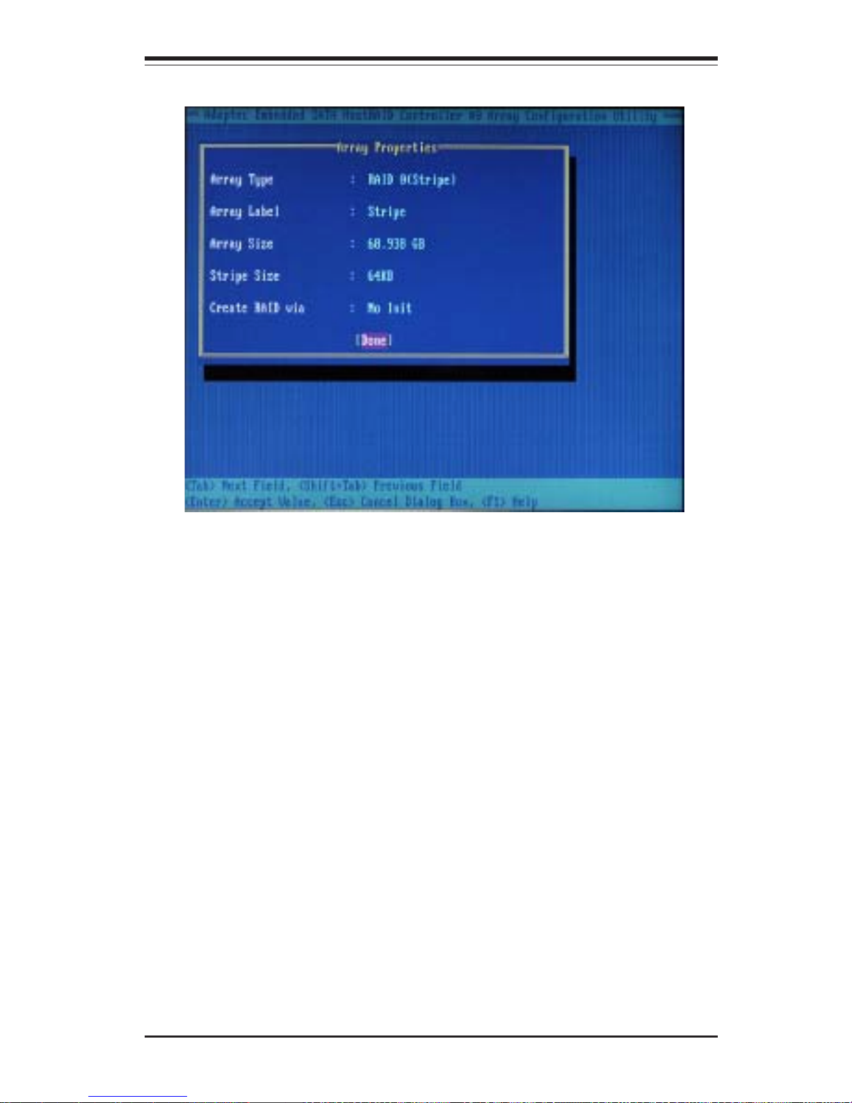
Appendix C: Software Installation Instructions
C-9
Notes:
1. Before adding a new drive to an array, back up any data contained on
the new drive. Otherwise, all data will be lost.
2. If you stop the Build or Clear process on a RAID 1 from ACU, you can
restart it by pressing Ctrl+R.
3. A RAID 1 created using the Quick Init option may return some data miscompares if you later run a consistency check. This is normal and is not
a cause for concern.
4. The ACU allows you to use drives of different sizes in a
RAID . However, during a build operation, only the smaller drive can be
selected as the source or first drive.
5. When migrating from single volume to RAID 0, migrating from a larger
drive to a smaller drive is allowed. However, the destination drive must
be at least half the capacity of the source drive.
6. Adaptec does not recommend that you migrate or build an array on
Windows dynamic disks (volumes), as it will result in data loss.
Warning: Do not interrupt the creation of a RAID 0 using the Migrate
option. If you do, you will not be able to restart, or to recover the data
that was on the source drive.
5. When you are finished, press Done (as the screen shown below).
Page 100
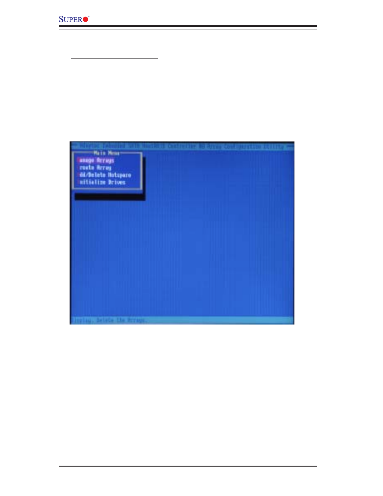
C-10
X6DAR-8G/X6DAR-iG User's Manual
Adding a Bootable Array
To make an array bootable:
1. From the Main menu, select Manage Arrays.
2. From the List of Arrays, select the array you want to make
bootable, and press Ctrl+B.
3. Enter Y to create a bootable array when the following message is
displayed: "This will make all other existing bootable array non-bootable. Do
you want to make this array bootable? (Yes/No):" Then, a bootable array
will be created. An asterisk will appear next to the bootable array (as
shown in the picture below:)
Deleting a Bootable Array
To delete a bootable array:
1. From the Main menu, select Manage Arrays.
2. From the List of Arrays, select the bootable array (*) you want to delete,
and press Ctrl+B. (* a bootable array is the array marked with an asterisk
(as shown in the picture above.)
3. Enter Y to delete a bootable array when the following message is
displayed: "The array is already marked bootable. Do you want to make this
array as not bootable? (Yes/No):" Then, the bootable array will be deleted
and the asterisk will disappear.
(*Note: do not use the delete key to delete the bootable array.)
 Loading...