

Supero X6DA8-G, X6DAE-G, X6DAE-G2, X6DA8-G2 User Manual

®
X6DA8-G
X6DAE-G
X6DA8-G2
X6DAE-G2
USER’S MANUAL
Revision 1.0c
SUPER

The information in this User’s Manual has been carefully reviewed and is believed to be
accurate. The vendor assumes no responsibility for any inaccuracies that may be
contained in this document, makes no commitment to update or to keep current the
information in this manual, or to notify any person or organization of the updates.
Please Note: For the most up-to-date version of this manual, please
see our web site at www.supermicro.com.
SUPERMICRO COMPUTER reserves the right to make changes to the product described in
this manual at any time and without notice. This product, including software, if any, and
documentation may not, in whole or in part, be copied, photocopied, reproduced, translated
or reduced to any medium or machine without prior written consent.
IN NO EVENT WILL SUPERMICRO COMPUTER BE LIABLE FOR DIRECT, INDIRECT,
SPECIAL, INCIDENTAL, OR CONSEQUENTIAL DAMAGES ARISING FROM THE USE OR
INABILITY TO USE THIS PRODUCT OR DOCUMENTATION, EVEN IF ADVISED OF THE
POSSIBILITY OF SUCH DAMAGES. IN PARTICULAR, THE VENDOR SHALL NOT HAVE
LIABILITY FOR ANY HARDWARE, SOFTWARE, OR DATA STORED OR USED WITH THE
PRODUCT, INCLUDING THE COSTS OF REPAIRING, REPLACING, INTEGRATING,
INSTALLING OR RECOVERING SUCH HARDWARE, SOFTWARE, OR DATA.
Any disputes arising between manufacturer and customer shall be governed by the laws of
Santa Clara County in the State of California, USA. The State of California, County of
Santa Clara shall be the exclusive venue for the resolution of any such disputes.
Supermicro's total liability for all claims will not exceed the price paid for the hardware
product.
Unless you request and receive written permission from SUPER MICRO COMPUTER, you
may not copy any part of this document.
Information in this document is subject to change without notice. Other products and
companies referred to herein are trademarks or registered trademarks of their respective
companies or mark holders.
Copyright © 2005 by SUPER MICRO COMPUTER INC.
All rights reserved.
Printed in the United States of America

iii
Preface
Preface
About This Manual
This manual is written for system integrators, PC technicians and
knowledgeable PC users. It provides information for the installation and use
of the X6DA8-G/X6DAE-G/X6DA8-G2/X6DAE-G2 motherboard. The
X6DA8-G/X6DAE-G/X6DA8-G2/X6DAE-G2 supports single or dual
Intel® Xeon NoconaTM processors at a 800 MHz front side bus. Based
upon Intel's NetBurst microarchitecture with EM64T support, the Nocona
processor supports the IA-32 software and includes features found in the
XeonTM processor such as Hyper Pipelined Technology, which includes a
multi-stage pipeline, allowing the processor to operate at much higher core
frequencies. Packaged in a 604-pin Flip Chip Micro Pin Grid Array(FCmPGA4) platform in a Zero Insertion Force(ZIF) socket (mPGA 604), the
Nocona Processor (800 MHz) supports Hyper-Threading Technology and
is ideal for high performance workstation and server environments with up
to two processors on one system bus. Please refer to the motherboard
specifications pages on our web site (http://www.supermicro.com/
Product_page/product-m.htm) for updates on supported processors. This
product is intended to be professionally installed.
Manual Organization
Chapter 1 begins with a checklist of what should be included in your
mainboard box, describes the features, specifications and performance of
the motherboard and provides detailed information about the chipset.
Chapter 2 begins with instructions on handling static-sensitive devices.
Read this chapter when you want to install the processor and DIMM memory
modules and when mounting the mainboard in the chassis. Also refer to
this chapter to connect the floppy and hard disk drives, SCSI drives, the IDE
interfaces, the parallel and serial ports, the keyboard and mouse, the power
supply and various control panel buttons and indicators.
If you encounter any problems, see Chapter 3, which describes troubleshooting procedures for the video, the memory and the setup configuration
stored in CMOS. For quick reference, a general FAQ [Frequently Asked
Questions] section is provided.
Chapter 4 includes an introduction to BIOS and provides detailed information on running the CMOS Setup utility.
Appendix A gives information on BIOS POST messages.
Appendix B provides software and the OS installation instructions.

iv
Preface
About This Manual ...................................................................................................... ii i
Manual Organization ................................................................................................... iii
Chapter 1: Introduction
1-1 Overview ......................................................................................................... 1-1
Checklist .................................................................................................... 1-1
Contacting Supermicro ............................................................................ 1-2
X6DA8-G/X6DAE-G/X6DA8-G2/X6DAE-G2 Image .............. 1-3
X6DA8-G/X6DAE-G/X6DA8-G2/X6DAE-G2 Layout ............. 1-4
Quick Reference ..................................................................................... 1-5
Motherboard Features ............................................................................. 1-6
Intel Tumwater Chipset: System Block Diagram ................................. 1-8
1-2 Chipset Overview........................................................................................... 1-9
1-3 Special Features........................................................................................... 1-10
1-4 PC Health Monitoring.................................................................................... 1-10
1- 5 ACPI Features ............................................................................................... 1-11
1-6 Power Supply ............................................................................................... 1-13
1- 7 Super I/O......................................................................................................... 1-13
Chapter 2: Installation
2-1 Static-Sensitive Devices ............................................................................... 2-1
Precautions............................................................................................... 2-1
Unpacking.................................................................................................. 2-1
2-2 PGA Processor and Heatsink Installation .................................................. 2-2
2-3 Installing DIMMs............................................................................................... 2-6
2- 4 I/O Ports/Control Panel Connectors ............................................................. 2-7
2-5 Connecting Cables .......................................................................................... 2-9
ATX Power Connector............................................................................ 2-9
Processor Power Connector................................................................. 2-9
NMI Button ................................................................................................ 2-10
Power LED ............................................................................................... 2-10
HDD LED .................................................................................................. 2-11
NIC1/NIC2 LED ........................................................................................ 2-11
Overheat LED ......................................................................................... 2-12
Power Fail LED ....................................................................................... 2-12
Reset Button ........................................................................................... 2-13
Power Button ......................................................................................... 2-13
Table of Contents
X6DA8-G/X6DAE-G/X6DA8-G2/X6DAE-G2 User's Manual

Table of Contents
v
Chassis Intrusion .................................................................................... 2-14
Universal Serial Bus.............................................................................. 2-14
ATX PS/2 Keyboard and Mouse Ports ................................................2-15
Fan Headers ........................................................................................... 2-15
Wake-On-Ring ......................................................................................... 2-16
Wake-On-LAN ......................................................................................... 2-16
GLAN (Ethernet Port) ............................................................................. 2-17
Power LED/Speaker Header (JD1) ..................................................... 2-17
Power Fault ............................................................................................. 2-18
Alarm Reset ............................................................................................. 2-18
SMB ........................................................................................................... 2-19
Overheat LED ..........................................................................................2-19
SMB PWR Connector .............................................................................. 2-20
AC'97 Audio Enable ................................................................................ 2-20
Keylock ..................................................................................................... 2-21
Serial Ports ............................................................................................. 2-21
2- 6 Jumper Settings ............................................................................................ 2-22
Explanation of Jumpers ........................................................................ 2-22
GLAN Enable/Disable............................................................................. 2-22
Power Supply Alarm Reset................................................................... 2-23
CMOS Clear............................................................................................. 2-24
Watch Dog Enable .................................................................................. 2-24
SCSI Control Enable................................................................................ 2-25
SCSI Termination Enable/Disable..........................................................2-25
PLLSEL Select ......................................................................................... 2-26
2-7 Onboard Indicators ...................................................................................... 2-27
GLAN LEDs.............................................................................................. 2-27
2- 8 Parallel Port, Floppy/Hard Disk Drive and SCSI Connections ............... 2-28
Parallel Port Connector ......................................................................... 2-28
Floppy Connector ................................................................................... 2-29
IDE Connectors ...................................................................................... 2-29
SCSI Connectors ..................................................................................... 2-30
Chapter 3: Troubleshooting
3-1 Troubleshooting Procedures ........................................................................ 3-1
Before Power On .................................................................................... 3-1
No Power .................................................................................................. 3-1
No Video ................................................................................................... 3-1
Memory Errors .......................................................................................... 3-2

vi
X6DA8-G/X6DAE-G/X6DA8-G2/X6DAE-G2 User's Manual
Losing the System’s Setup Configuration ........................................... 3-2
3-2 Technical Support Procedures .................................................................... 3-2
3-3 Frequently Asked Questions........................................................................ 3-3
3-4 Returning Merchandise for Service............................................................ 3-4
Chapter 4: BIOS
4- 1 Introduction....................................................................................................... 4-1
4- 2 Running Setup .................................................................................................. 4-2
4- 3 Main BIOS Setup.............................................................................................. 4-2
4-4 Advanced Setup.............................................................................................. 4-7
4-5 Security Setup...............................................................................................4-19
4- 6 Boot Setup...................................................................................................... 4-21
4-7 Exit ................................................................................................................... 4-22
Appendices:
Appendix A: BIOS POST Messages ..................................................................... A-1
Appendix B: Installing Software Drivers and the Operating System ..............B-1

Chapter 1: Introduction
1-1
Introduction
Chapter 1
Introduction
1-1 Overview
Checklist
Congratulations on purchasing your computer motherboard from an acknowledged leader in the industry. Supermicro boards are designed with
the utmost attention to detail to provide you with the highest standards in
quality and performance. Check that the following items have all been included with your motherboard. If anything listed here is damaged or missing, contact your retailer. All included with Retail Box.
One (1) Supermicro Mainboard
One (1) ribbon cable for IDE devices
One (1) floppy ribbon cable
One (1) SCSI-U320 cable (*X6DA8-G/X6DA8-G2)
One (1) SATA cable
One (1) I/O backpanel shield
One (1) Supermicro CD containing drivers and utilities
One (1) User's/BIOS Manual
One (1) SCSI User's Manual (*X6DA8-G/X6DA8-G2)
Two (2) CPU Mounting Brackets (SKT-0158) (pre-installed)

1-2
Introduction
X6DA8-G/X6DAE-G/X6DA8-G2/X6DAE-G2 User's Manual
Contacting Supermicro
Headquarters
Address: SuperMicro Computer, Inc.
980 Rock Ave.
San Jose, CA 95131 U.S.A.
Tel: +1 (408) 503-8000
Fax: +1 (408) 503-8008
Email: marketing@supermicro.com (General Information)
support@supermicro.com (Technical Support)
Web Site: www.supermicro.com
Europe
Address: SuperMicro Computer B.V.
Het Sterrenbeeld 28, 5215 ML
's-Hertogenbosch, The Netherlands
Tel: +31 (0) 73-6400390
Fax: +31 (0) 73-6416525
Email: sales@supermicro.nl (General Information)
support@supermicro.nl (Technical Support)
rma@supermicro.nl (Customer Support)
Asia-Pacific
Address: SuperMicro, Taiwan
4F, No. 232-1 Liancheng Road
Chung-Ho 235, Taipei County, Taiwan, R.O.C.
Tel: +886-(2) 8226-3990
Fax: +886-(2) 8226-3991
Web Site: www.supermicro.com.tw
Technical Support:
Email: support@supermicro.com.tw
Tel: 886-2-8228-1366, ext.132 or 139
Chapter 1: Introduction
1-3
Introduction
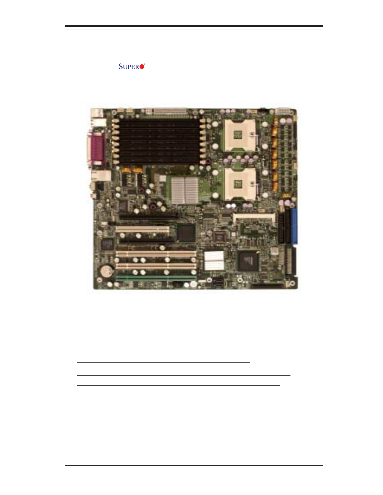
Figure 1-1. X6DA8-G/X6DAE-G/X6DA8-G2/X6DAE-G2 Image
*Notes: The differences between these models are:
1.SCSI is available for the X6DA8-G/X6DA8-G2 only.
2. There are two Gigabit LAN ports on the X6DA8-G2/X6DAE-G2
and only one Gigabit LAN on the X6DA8-G and the X6DAE-G.
1-4
Introduction
X6DA8-G/X6DAE-G/X6DA8-G2/X6DAE-G2 User's Manual
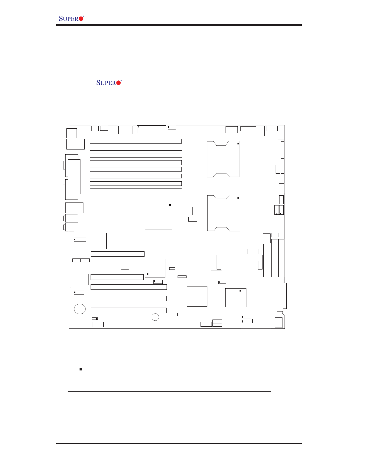
Figure 1-2. X6DA8-G/X6DAE-G/X6DA8-G2/X6DAE-G2 Motherboard
Layout
1. Jumpers not indicated are for test purposes only.
(not drawn to scale)
2. See Chapter 2 for detailed information on jumpers, I/O ports and
JF1 front panel connections.
3. " " indicates the location of Pin 1.
4. SCSI is available for the X6DA8-G/X6DA8-G2 only.
5. There are two Gigabit LAN ports on the X6DA8-G2/X6DAE-G2
and only one Gigabit LAN on the X6DA8-G and the X6DAE-G.
6. The graphics shown in this manual were based upon the latest PCB
Revision available at the time of publishing of this manual. The
motherboard you've received may or may not look exactly the same as
the graphics shown in this manual.
KB/
Mouse
DIMM 4A
DIMM 4B
DIMM 3A
DIMM 3B
DIMM 2A
DIMM 2B
DIMM 1A
DIMM 1B
SPKR
GLAN
Enable
Tumwater
(NorthBridge)
(South
Bridge)
IPMI 2.0
BIOS
7902
SCSI
CTRL
IDE #1
IDE #2
Floppy
Fan4
FPUSB 6/7
JD2
SATA0
JPA3
FP CTRL
JF1
FAN7
PW SMB
CPU1
CPU2
J9
J40
J3
J4
JP8
JD1
J24
XJ4F2
USB 0/
1/2/3
JLAN1
COM2
COM1
Parrallel
Port
Fan6
Fan5
J32
4-pin
PWR
Bank 1
Bank 1
Bank 2
Bank 2
Bank 3
Bank 3
Bank 4
Bank 4
ATX PWR
J1B4
JPF
Force
PW
(**JLAN)
Line_In/
Line_Out
XJ4F1
PLL Select
(X8DA8/E-G)
JPC1
Audio
Enable
SI/O
x16 PCI EXP #6
PCI #5-33MHz
PCIX#3-133MHz
PCIX#2-100MHz
J27
BIOS Debug
CD1
CD2
PCIX#1-100MHz ZCR
GLAN
CTRL
JPL1
Battery
JWOR
SMBus
J22
SATA1
SCSI Ch B
JPA2
SCSI Ch A
JA1
JA2
Fan3
Cha.
Intru
JPA1
SCSI CTRL
Enable
J20
JWD
WD
JK1
Keylock
Fan8
JBT1
Clear
cmos
FAN1
3rd PS
AlmEna
OH
LED
PWR
LED
SPKR
ICH
SPKR
J1D1
12V 8pinPW
SCSI Ch.A
Term.
SCSICh.B
Term.
JC2
Mic
JC1
x4 PCI EXP #4
JWOL
JL1
JP13
JP14
JOH1
JP15
PW
Fault
JP12
PXH
LAN
USB4/5
JD3
FAN2
WOL
WOR
PW Fail
Alm Rst

Chapter 1: Introduction
1-5
Introduction
Jumper Description Default Setting
JP13 3rd PWR Supply Failure Enable Open (Disabled)
JPA1 SCSI Controller Enabled(X6DA8-G/G2)Pins 1-2 (Enabled)
JPA2/JPA3 SCSI Ch. A/B Term.Ena.(X6DA8-G/G2)Open(Enabled)
JPC1 Audio Enable/Disable Pins 1-2 (Enabled)
JPF Force Power Open (Disabled)
JPL1 Giga-bit LAN Enable/Disable Pins 1-2 (Enabled)
JWD Watch Dog Enable Pins 1-2 (Reset)
XJ4F1/XJ4F2 PLL Select (*X6DA8-G/X6DAE-G) Closed (333MHz)
Connector Description
ATX PWR (J1B4) Primary 24-pin ATX PWR Connector
12V PWR (J1D1, J32) 12V 8-pin PWR/12V 4-pin CPU PWR Connectors
COM1 (J6)/COM2 (J39) COM1/COM2 Serial Port Connectors
FAN #1-#8 CPU Fan1/CPU Fan2/Chassis Fans Headers
DIMM#1A-#4B Memory (RAM) Slots#(1A,1B, 2A,2B, 3A,3B,4A,4B)
GLAN1 G-bit Ethernet Ports
GLAN2 G-bit Ethernet Ports (*X6DA8-G2/DAE-G2 only)
IDE1(J3), IDE2(J4) IDE1/2 Hard Disk Drive Connectors
J9 Keyboard/Mouse
J20 IPMI 2.0 Connector
J22 System Management Bus Connector
J23 Parallel (Printer) Port
J24 PWR System Management Bus
JA1, JA2 Ultra 320 SCSI Channel A,Channel B(X6DA8-G/G2)
JBT1 CMOS Clear (JBT1 is a pad:See Chapter 2)
JD1 PWR LED (Pins1-3), Speaker (Pins 4-7)
JF1 Front Panel Control
JK1 Keylock
JL1 Chassis Intrusion Header
JOH1 Overheat LED
JP8 Floppy Disk Drive Connector
JP12 Power Fault Connector
JP14 PWR Fail Alarm Reset
PCIX#1,#2,#3(J12-J14) PCIX-100MHz ZCR,PCIX-100MHz/PCIX-133MHzslots
PCI#5(J19) PCI-33 MHz slot
PCI-Express#4,#6 x4/x16 PCI-Express slots
SATA0/1 Serial ATA0/Serial ATA1 Headers
JWOL Wake-on-LAN Header
JWOR1 Wake-on-Ring Header
USB#0-3(J40) (Back Panel) Universal Serial Bus Ports
USB#4-5,6-7(JD3, JD2) (Front Panel) Universal Serial Bus Headers
Quick Reference

1-6
Introduction
X6DA8-G/X6DAE-G/X6DA8-G2/X6DAE-G2 User's Manual
Motherboard Features
CPU
• Single or dual Intel® 604-pin 64-bit/32-bit NoconaTM processors at 800
MHz front side (system) bus speed. (*Notes: CPU FSB
speed is set by Manufacturer. Please refer to the support section of our web site for a complete
listing of supported processors (http://www.supermicro.com/TechSupport.htm.)
Memory
• Eight 240-pin DIMM sockets supporting up to 16 GB Registered ECC
DDR2-400 (PC3200) SDRAM (*X6DA8-G2/X6DAE-G2 only)
• Eight 184-pin DIMM sockets supporting up to 32 GB Registered ECC
DDR-333/266 (PC2700/PC2100)SDRAM(-16 GB for PC2700, 32GB for
PC2100) (*X6DA8-G/X6DAE-G only)
Notes: 1. Memory size is set via BIOS. 2. Interleaved memory; requires memory modules to be
installed in pairs. See Section 2-3 for details.
Chipset
• Intel E7525 (Tumwater) chipset
Expansion Slots
• One PCI-e slot (*x16@4GB/sec)
• One PCI-e slot (*x4@2GB/sec)
• Three 64-bit PCI-X slots (*One 64-bit PCI-X-133 slot, one PCI-X-100
slot, One PCI-X-100MHz ZCR)
• One 32-bit 33MHz PCI slot (w/PCI Graphic Card support)
BIOS
• 8 Mb Phoenix BIOS ROM
• APM 1.2, DMI 2.1, PCI 2.2, ACPI 1.0, Plug and Play (PnP), SMBIOS 2.3
PC Health Monitoring
• Onboard voltage monitors for CPU cores, chipset voltage, 3.3V, +5V,
+12V, -12V and 3.3V standby
• Fan status monitor by Thermal Management via BIOS
• CPU/chassis temperature monitors
• Environmental temperature monitor via Supero Doctor III
• CPU fan auto-off in sleep mode
• CPU slow-down on temperature overheat
• CPU thermal trip support for processor protection, +5V standby alert

Chapter 1: Introduction
1-7
Introduction
LED
• Power-up mode control for recovery from AC power loss
• System overheat LED and control
• Chassis intrusion detection
• System resource alert via Super Doctor III
ACPI Features
• Microsoft OnNow
• Slow blinking LED for suspend state indicator
• Main switch override mechanism
Onboard I/O
• Adaptec 7902 dual channel Ultra 320 SCSI (*X6DA8-G/X6DA8-G2 only)
• One IPMI 2.0
• One Intel 8254x Gigabit Ethernet controller(*X6DA8/X6DAE-G:1 LAN,
X6DA8/X6DAE-G2:2 LAN ports)
• 2 EIDE Ultra DMA/100 bus master interfaces
• 1 floppy port interface (up to 2.88 MB)
• 1 EPP/ECP Parallel Port
• PS/2 mouse and PS/2 keyboard ports
• Up to eight USB 2.0 (Universal Serial Bus):
(4 Back Panel USB ports & 4 Front Panel USB headers)
• 2 serial ports
• 2 Serial ATA support (w/RAID 0/RAID 1 support)
Other
• Internal/external modem ring-on
• Wake-on-Ring (WOR)
• Wake-on-LAN (WOL)
• Console redirection
CD/Diskette Utilities
• BIOS flash upgrade utility and device drivers
Dimensions
• ATX Ext. 12" x 13.05" (304.8 x 331.5 mm)
1-8
Introduction
X6DA8-G/X6DAE-G/X6DA8-G2/X6DAE-G2 User's Manual
MC H
NOCONA P R OCE S SOR # 2VRM
CL OCK
ADDR
CTRL
DAT A
NOCONA P R OCE S SOR # 1
ADDR
CTRL
DAT A
DAT A
ADDR
CTRL
ICH5R
HUB
DDRI I - 40 0
A
PXH
B
PCI EXP. A
1 PCI - X
SLOT 3
1 PCI - X
PCI - X BUS( 100 MHZ)
Gbi t L AN
SLOT 2
J13
PCI - X BUS( 100 MHZ)
J14
1 PCI - EXP
SLOT 4
J17
PCI EXP. B, C ( X16)
J15
1 PCI - EXP
S L OT 6
DI MMs
IDE
PRI / SEC
UDMA/ 100
X8X4
X4
DI MMs
0, 1
SATA
SATA
LPC BUSUS B
US B POR T
0, 1, 2, 3,
BMC CON. F WHLPC I / O
PARALLE L
PORT
MS .
FDD. SER. 1
SER. 2
KB.
4 DDR II - 400
4 DDR II - 400
DDRI I - 40 0
SCSI
7902
PCI BUS( 32 - BI T )
PCI 3 2 BI T
S L OT 5
AC 9 7
J19
1 PCI - X
SLOT 1
J12
H/ W
MO N I T OR
5, 6, 7, 8
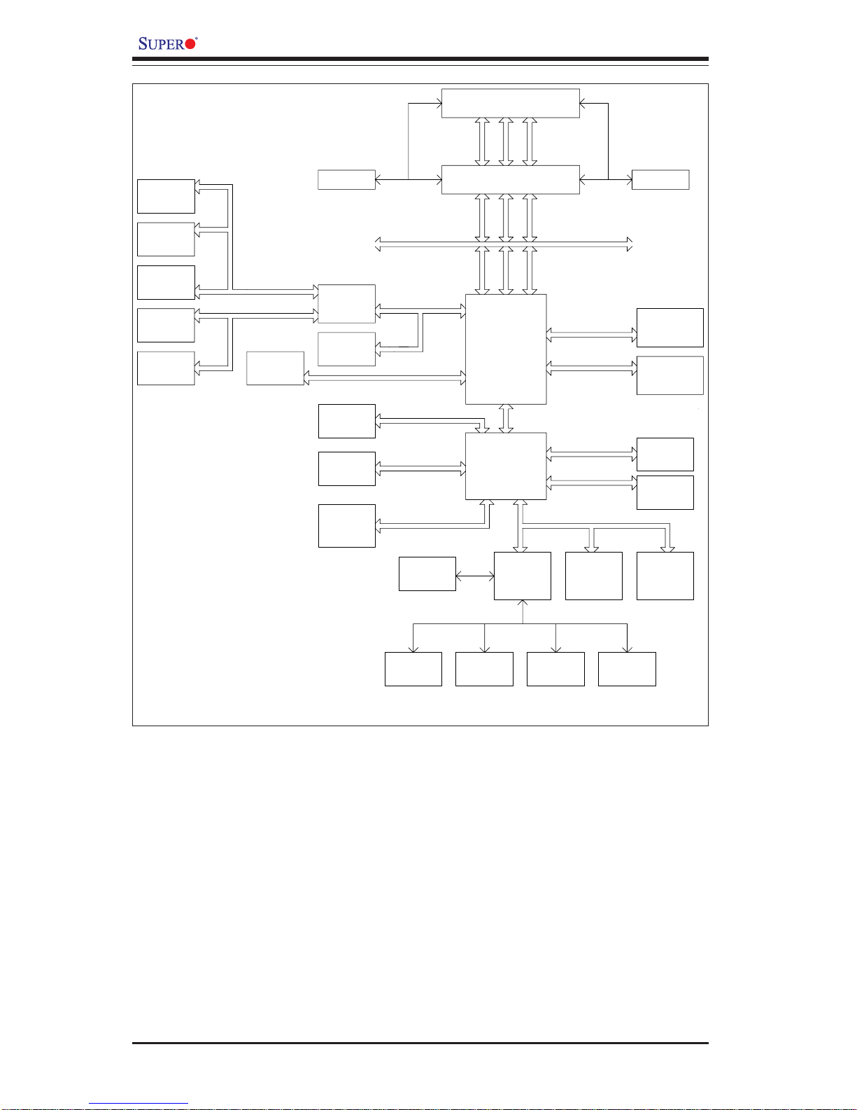
Figure 1-9. Block Diagram of the E7525 Tumwater Chipset
Note: This is a general block diagram. Please see the previous Motherboard
Features pages for details on the features of each motherboard.

Chapter 1: Introduction
1-9
Introduction
1-2 Chipset Overview
Built upon the functionality and the capability of the E7525 Tumwater
chipset, the X6DA8-G/X6DAE-G/X6DA8-G2/X6DAE-G2 motherboard provides the performance and feature set required for dual processor-based
computer systems, with configuration options optimized for communications,
presentation, storage, computation or database applications. The Intel E7525
Tumwater chipset consists of the following components: the E7525
Tumwater Memory Controller Hub (MCH), the I/O Controller Hub ( ICH5R),
and the PCI-X Hub (PXH).
The E7525 Tumwater MCH supports single or dual Nocona processors with
Front Side Bus speeds of up to 800 MHz(*Note). Its memory controller provides direct connection to two channels of registered DDR333 or DDR2 400
with a marched system bus address and data bandwidths of up to 2.67 GB/
s (DDR 333) or 3.2 GB/s (DDR2-400) per channel. The E7525 Tumwater
also supports the new PCI Express high speed serial I/O interface for superior I/O bandwidth. The MCH provides configurable x16 PCI Express interfaces which may alternatively be configured as two independent x8 PCI
Express interfaces. These interfaces support connection of the MCH to a
variety of other bridges that are compliant with the PCI Express Interface
Specification, Rev. 1.0a, such as 82546GB GLAN Adaptor, the Dobson I/O
processor, H/W RAID controllers and TCP/IP Off-load engines. The MCH
interfaces with the ICH5R ICH I/O Controller Hub via HI 1.5 Hub Interface.
The PXH can be configured to support for 32- or 64-bit PCI devices running
at 33 MHz, 66 MHz, 100 MHz, and 133 MHz.
ICH5R System Features
In addition to providing the I/O subsystem with access to the rest of the
system, the ICH5R I/O Controller Hub integrates many I/O functions.
The ICH5 I/O Controller Hub integrates: 2-channel Ultra ATA/100 Bus Master IDE Controller, two Serial ATA (SATA) Host w/RAID0, RAID1 support,
SMBus 2.0 Controller, LPC/Flash BIOS Interface, PCI 2.2 Interface and System Management Controller.
(*Notes: The CPU FSB speed is set at 800 MHz by the Manufacturer.)

1-10
Introduction
X6DA8-G/X6DAE-G/X6DA8-G2/X6DAE-G2 User's Manual
1-3 Special Features
Recovery from AC Power Loss
BIOS provides a setting for you to determine how the system will respond
when AC power is lost and then restored to the system. You can choose
for the system to remain powered off (in which case you must hit the
power switch to turn it back on) or for it to automatically return to a poweron state. See the Power Lost Control setting in the Advanced BIOS Setup
section (Boot Features) to change this setting. The default setting is Always On.
1-4 PC Health Monitoring
This section describes the PC health monitoring features of the SUPER
X6DA8-G/X6DAE-G/X6DA8-G2/X6DAE-G2. All have an onboard System
Hardware Monitor chip that supports PC health monitoring.
Onboard Voltage Monitors for the CPU Cores, Chipset
Voltage, +3.3V, +5V, +12V, -12V and +3.3V Standby
An onboard voltage monitor will scan these voltages continuously. Once a
voltage becomes unstable, a warning is given or an error message is sent
to the screen. Users can adjust the voltage thresholds to define the
sensitivity of the voltage monitor.
Fan Status Monitor with Firmware/Software On/Off Control
The PC health monitor can check the RPM status of the cooling fans. The
onboard 4-pin CPU and chassis fans are controlled by the power management functions. The thermal fan is controlled by the overheat detection
logic.
Environmental Temperature Control via Supero DoctorIII
The thermal control sensor monitors the CPU temperature in real time and
will turn on the thermal control fan whenever the CPU temperature exceeds
a user-defined threshold. The overheat circuitry runs independently from
the CPU. It can continue to monitor for overheat conditions even when the
CPU is in sleep mode. Once it detects that the CPU temperature is too high,
it will automatically turn on the thermal control fan to prevent any overheat

Chapter 1: Introduction
1-11
Introduction
damage to the CPU. The onboard chassis thermal circuitry can monitor the
overall system temperature and alert users when the chassis temperature
is too high.
CPU Fan Auto-Off in Sleep Mode
The CPU fan activates when the power is turned on. It continues to operate
when the system enters Standby mode. When in sleep mode, the CPU will
not run at full power, thereby generating less heat.
CPU Overheat LED and Control
This feature is available when the user enables the CPU overheat warning
function in the BIOS. This allows the user to define an overheat temperature. When this temperature is exceeded, both the overheat fan and the
warning LED are triggered.
System Resource Alert (via Supero DoctorIII)
This feature is available when used with Intel's LANDesk Client Manager
(optional). LDCM is used to notify the user of certain system events. For
example, if the system is running low on virtual memory and there is insufficient hard drive space for saving the data, you can be alerted of the
potential problem.
Auto-Switching Voltage Regulator for the CPU Core
The auto-switching voltage regulator can auto-detect and regulate power
supply to the CPU. This will allow the regulator to run cooler and thus make
the system more stable.
1-5 ACPI Features
ACPI stands for Advanced Configuration and Power Interface. The ACPI
specification defines a flexible and abstract hardware interface that provides a standard way to integrate power management features throughout
a PC system, including its hardware, operating system and application software. This enables the system to automatically turn on and off peripherals
such as CD-ROMs, network cards, hard disk drives and printers. This also
includes consumer devices connected to the PC such as VCRs, TVs, telephones and stereos.

1-12
Introduction
X6DA8-G/X6DAE-G/X6DA8-G2/X6DAE-G2 User's Manual
In addition to enabling operating system-directed power management, ACPI
provides a generic system event mechanism for Plug and Play and an operating system-independent interface for configuration control. ACPI leverages the Plug and Play BIOS data structures while providing a processor
architecture-independent implementation that is compatible with Windows
2000, Windows XP, Windows NT 5.0 and Windows 2003.
Microsoft OnNow
The OnNow design initiative is a comprehensive, system-wide approach to
system and device power control. OnNow is a term for a PC that is always
on but appears to be off and responds immediately to user or other requests.
Slow Blinking LED for Suspend-State Indicator
When the CPU goes into a suspend state, the chassis power LED will start
blinking to indicate that the CPU is in suspend mode. When the user presses
any key, the CPU will wake-up and the LED will automatically stop blinking
and remain on.
Main Switch Override Mechanism
When an ATX power supply is used, the power button can function as a
system suspend button to make the system enter a SoftOff state. The
monitor will be suspended and the hard drive will spin down. Depressing
the power button again will cause the whole system to wake-up. During
the SoftOff state, the ATX power supply provides power to keep the required circuitry in the system alive. In case the system malfunctions and
you want to turn off the power, just depress and hold the power button for
4 seconds. This option can be set in the Power section of the BIOS Setup
routine.
External Modem Ring-On (WOR)
Wake-up events can be triggered by a device such as the external modem
ringing when the system is in the SoftOff state. Note that external modem
ring-on can only be used with an ATX 2.01 (or above) compliant power
supply.

Chapter 1: Introduction
1-13
Introduction
1-6 Power Supply
As with all computer products, a stable power source is necessary for
proper and reliable operation. It is even more important for processors that
have high CPU clock rates.
The SUPER X6DA8-G/X6DAE-G/X6DA8-G2/X6DAE-G2 accommodates ATX
power supplies. Although most power supplies generally meet the specifications required by the CPU, some are inadequate. You should use one
that will supply at least 400W of power (*Note: the 12V 8-pin power
connector (J1D1) is required for CPU power consumption, and an
additional 12V 4-pin power connection (J32) is also required to
ensure adequate power supply to the system.) Also your power sup-
ply must supply 1.5A for the Ethernet ports. It is strongly recommended that
you use a high quality power supply that meets ATX power supply Specification 2.02 or above. It must also be SSI compliant (info at http://
www.ssiforum.org/). Additionally, in areas where noisy power transmission is present, you may choose to install a line filter to shield the computer
from noise. It is recommended that you also install a power surge protector
to help avoid problems caused by power surges.
1-7 Super I/O
The disk drive adapter functions of the Super I/O chip include a floppy disk
drive controller that is compatible with industry standard 82077/765, a data
separator, write pre-compensation circuitry, decode logic, data rate selection, a clock generator, drive interface control logic and interrupt and DMA
logic. The wide range of functions integrated onto the Super I/O greatly
reduces the number of components required for interfacing with floppy disk
drives. The Super I/O supports 360 K, 720 K, 1.2 M, 1.44 M or 2.88 M disk
drives and data transfer rates of 250 Kb/s, 500 Kb/s or 1 Mb/s.It also
provides two high-speed, 16550 compatible serial communication ports
(UARTs), one of which supports serial infrared communication. Each UART
includes a 16-byte send/receive FIFO, a programmable baud rate generator,
complete modem control capability and a processor interrupt system. Both
UARTs provide legacy speed with baud rate of up to 115.2 Kbps as well as
an advanced speed with baud rates of 250 K, 500 K, or 1 Mb/s, which
support higher speed modems.
The Super I/O supports one PC-compatible printer port (SPP), Bi-directional
Printer Port (BPP) , Enhanced Parallel Port (EPP) or Extended Capabilities
Port (ECP).

1-14
Introduction
X6DA8-G/X6DAE-G/X6DA8-G2/X6DAE-G2 User's Manual
figuration and Power Interface), which includes support of legacy and ACPI
power management through an SMI or SCI function pin. It also features
auto power management to reduce power consumption.
The IRQs, DMAs and I/O space resources of the Super I/O can flexibly
adjust to meet ISA PnP requirements, which support ACPI and APM (Advanced Power Management).
The Super I/O provides functions that comply with ACPI (Advanced Con-

Chapter 2: Installation
2-1
Chapter 2
Installation
2-1 Static-Sensitive Devices
Electric-Static-Discharge (ESD) can damage electronic components. To prevent damage to your system board, it is important to handle it very carefully.
The following measures are generally sufficient to protect your equipment
from ESD.
Precautions
• Use a grounded wrist strap designed to prevent static discharge.
• Touch a grounded metal object before removing the board from the antistatic bag.
• Handle the board by its edges only; do not touch its components, peripheral chips, memory modules or gold contacts.
• When handling chips or modules, avoid touching their pins.
• Put the motherboard and peripherals back into their antistatic bags when
not in use.
• For grounding purposes, make sure your computer chassis provides excellent conductivity between the power supply, the case, the mounting
fasteners and the motherboard.
• Use only the correct type of onboard CMOS battery as specified by the
manufacturer. Do not install the onboard battery upside down to avoid
possible explosion.
Unpacking
The motherboard is shipped in antistatic packaging to avoid static damage.
When unpacking the board, make sure the person handling it is static protected.
Chapter 2: Installation
2-2
IMPORTANT: Always connect the power cord last and always remove it
before adding, removing or changing any hardware components. Make
sure that you install the processor into the CPU socket before you install
the CPU heat sink.
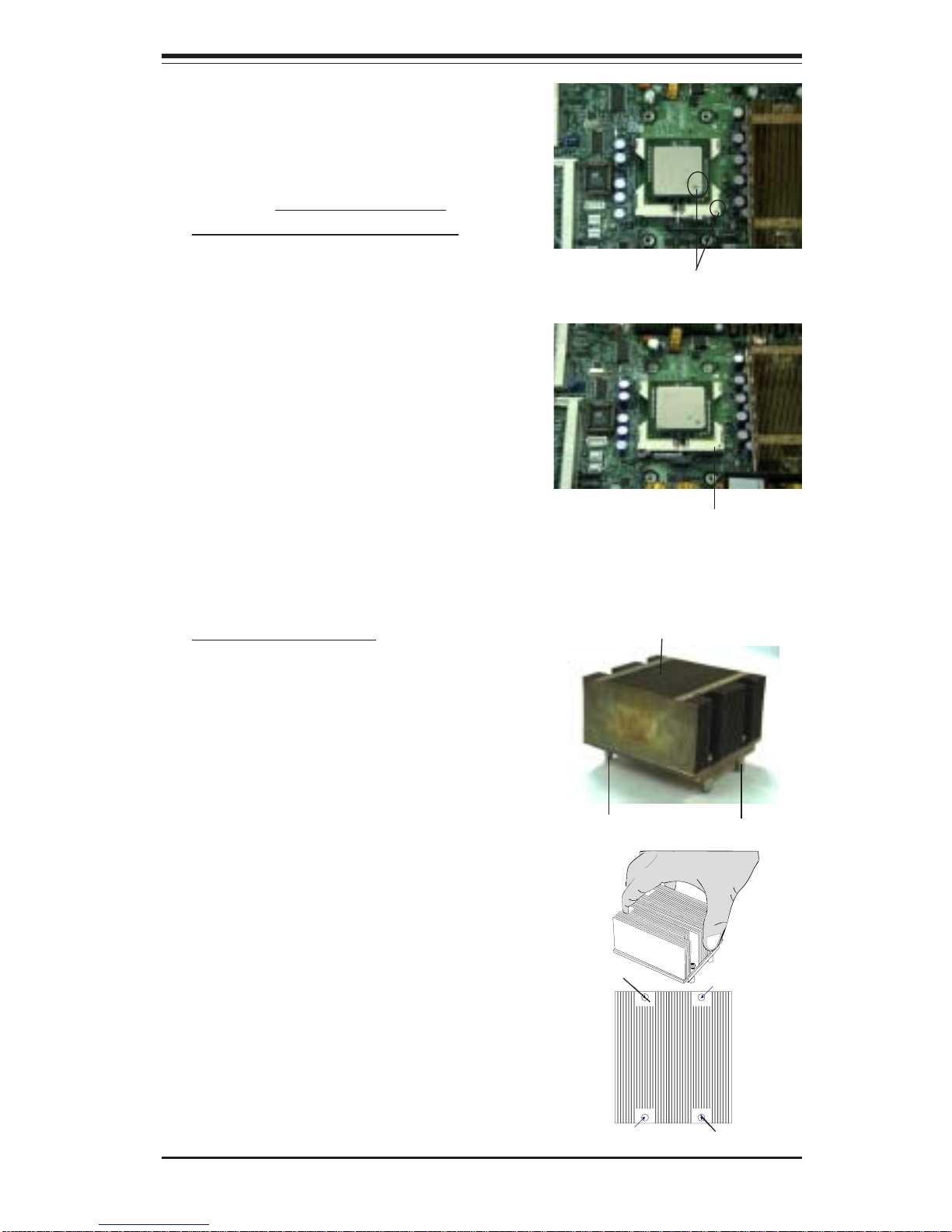
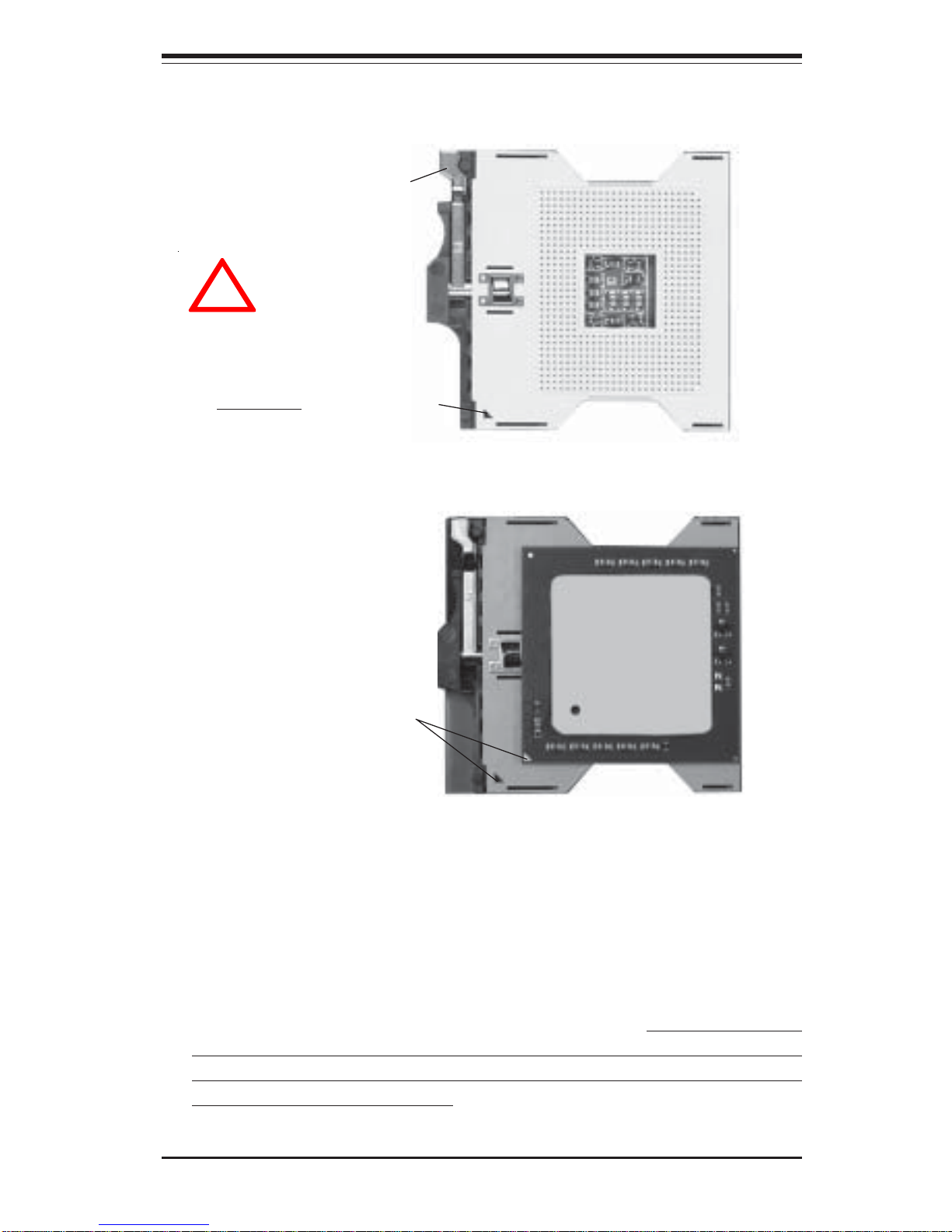
2-2 Nocona Processor and Heatsink Installation
When handling the processor package, avoid placing direct
pressure on the label area of the fan. Also, do not place the
motherboard on a conductive surface, which can damage the
BIOS battery and prevent the system from booting up.
!
Socket lever
CPU Installation
1. Lift the lever on the CPU socket:
lift the lever completely as shown
on the picture on the right;
otherwise, you will damage the
CPU socket when power is
applied. (Install CPU1 first.)
(*CPU Retention Plates are preinstalled. Pictures shown on right
are for reference only.)
CPU Retention
Bracket
CPU Socket
Mounting Holes
Xeon CPU
Heatsink
Chassis
back plane
Motherboard
CPU
Socket
Heatsink
Installing Retention Brackets
CPU
Standoffs
Mounting
Holes
Chassis
back plane
Chapter 2: Installation
2-3
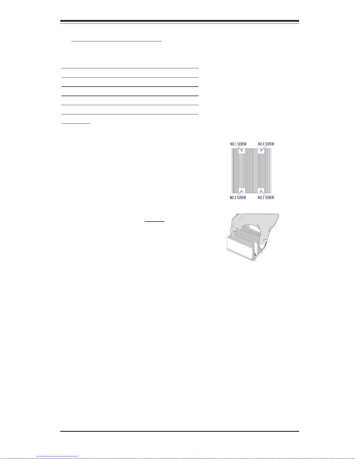
Heatsink
Heatsink Installation
1. Do not apply any thermal compound
to the heatsink or the CPU die-the
required amount has already been
applied.
2. Place the heatsink on top of the
CPU so that the four mounting holes
are aligned with those on the retention
mechanism.
3. Screw in two diagonal screws (ie
the #1 and the #2 screws) until just
snug (-do not fully tighten the screws
to avoid possible damage to the CPU.)
4. Finish the installation by fully
tightening all four screws.
Screw#1
Screw#2
Pin 1
2. Insert the CPU in the socket,
making sure that pin 1 of the CPU
aligns with pin 1 of the socket
(both corners are marked with a
triangle). When using only one
CPU, install it into CPU socket #1
(socket #2 is automatically disabled
if only one CPU is used).
3. Press the lever down until
you hear the *click* so you
can be sure that the CPU is
securely installed in the CPU
socket.
Socket lever in the
locking Position
Screw#1
Screw#2
Chapter 2: Installation
2-4
To Un-install the Heatsink
(Caution! We do not recommend that the
CPU or the heatsink be removed. However, if you do need to un-install the
heatsink, please follow the instructions
below to uninstall the heatsink to prevent
damage done to the CPU or the CPU
socket. )
1. Unscrew and remove the heatsink
screws from the motherboard in the
sequence as show in the picture on
the right.
2. Hold the heatsink as show in the
picture on the right and
gently wriggle
the heatsink to loosen it from the CPU.
(Do not use excessive force when
wriggling the heatsink!!)
3. Once the CPU is loosened from the
heatsink, remove the heatsink from
the CPU socket.
4. Clean the surface of the CPU and
the heatsink to get rid of the old thermal grease. Reapply the proper
amount of thermal grease on the surface before you re-install the CPU and
the heatsink.
Chapter 2: Installation
2-5
Figure 2-1. PGA604 Socket: Empty and with Processor Installed
Mounting the Motherboard in the Chassis
All motherboards have standard mounting holes to fit different types of
chassis. Make sure that the locations of all the mounting holes for both the
motherboard and the chassis match. Although a chassis may have both
plastic and metal mounting fasteners, metal ones are highly recommended
because they ground the motherboard to the chassis. Make sure that the
metal standoffs click in or are screwed in tightly. Then, use a screwdriver
to secure the motherboard onto the motherboard tray. (*Note: some components are very close to the mounting holes. Please take precautionary
measures to prevent damage done to these components when you install
the motherboard to the chassis.)
Lever
Processor
(installed)
Triangle
Triangle
Empty socket
Warning! Make
sure you lift the
lever completely
when installing the
CPU. If the lever is
only partly raised,
damage to the
socket or CPU may
result.
!
Chapter 2: Installation
2-6
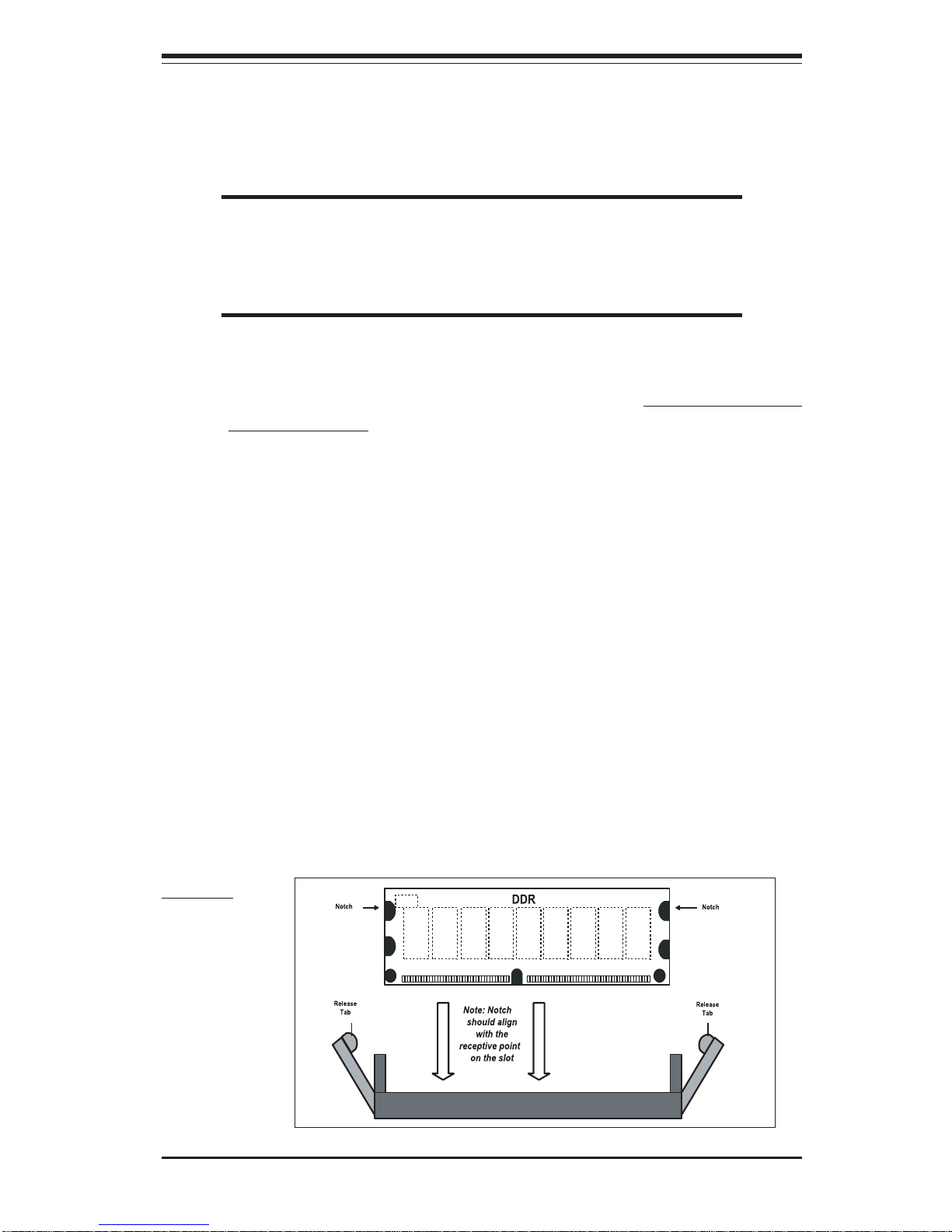
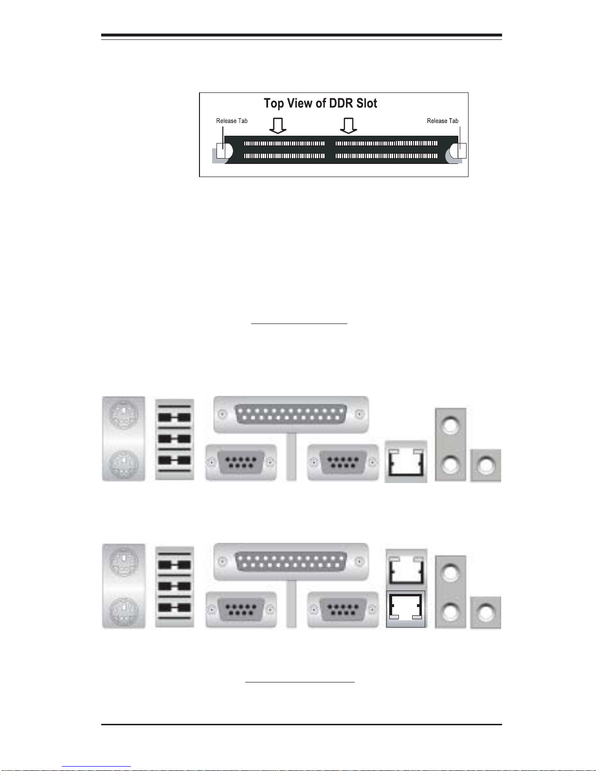
2-3 Installing DIMMs
Note: Check the Supermicro web site for recommended memory modules.
CAUTION
Exercise extreme care when installing or removing DIMM
modules to prevent any possible damage. Also note that the
memory is interleaved to improve performance (see step 1).
DIMM Installation (See Figure 2-2)
1. Insert the desired number of DIMMs into the memory slots, starting with
DIMM #1A. The memory scheme is interleaved so you must install two
modules at a time, beginning with DIMM #1A, then DIMM #1B, and so on.
2. Insert each DIMM module vertically into its slot. Pay attention to the
notch along the bottom of the module to prevent inserting the DIMM
module incorrectly.
3. Gently press down on the DIMM module until it snaps into place in the
slot. Repeat for all modules (see step 1 above).
Memory Support
The X6DA8-G2/X6DAE-G2 supports up to 16 GB of Reg. ECC DDR2 400
(PC3200) memory. The X6DA8-G/X6DAE-G supports up to 32 GB of Registered ECC DDR 333/266 (PC2700/PC2100) memory. (*The motherboard supports up to 32GB for PC2100, 16 GB for PC 2700.) All motherboards were
designed to support 4 GB modules in each slot, but has only been verified
for up to 2 GB modules. (*For DDR333: Maximum of 4 double-banked memory
modules, or maximum of 6 single-banked memory modules are supported.)
To Install:
Insert module
vertically and
press down
until it snaps
into place.
Pay attention
to the
alignment
notch at the
bottom.
Figure 2-2. Installing and Removing DIMMs
Chapter 2: Installation
2-7
To Remove:
Use your thumbs
to gently push
near the edge of
both ends of the
module. This
should release it
from the slot.
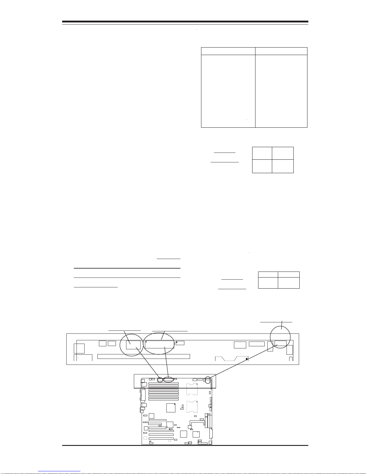
2-4 I/OPorts/Control Panel Connectors
The I/O ports are color coded in conformance with the PC 99 specification.
See Figure 2-3 below for the colors and locations of the various I/O ports.
Figure 2-3. I/O Port Locations and Definitions
*X6DA8-G2/X6DAE-G2
Parallel Port
COM1 & COM2
KB/Mouse
USB#0-3
LAN1
Line-In
Mic
*X6DA8-G/X6DAE-G
COM1 & COM2
LAN1/2
KB/Mouse
USB#0-3 Parallel Port
Line-out
Line-out
Line-In
Mic
Chapter 2: Installation
2-8
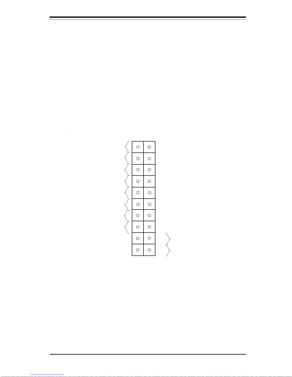
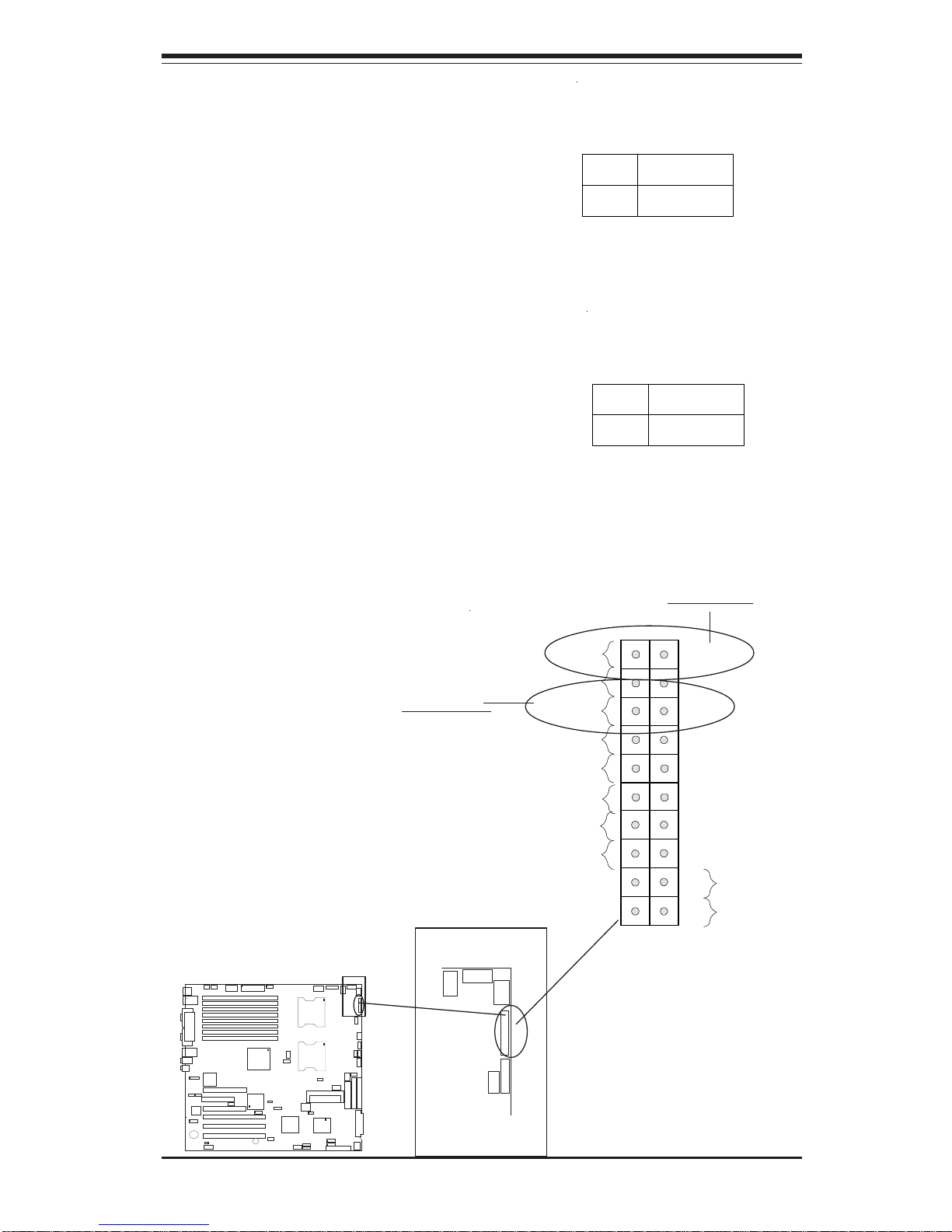
Front Control Panel
JF1 contains header pins for various buttons and indicators that are normally located on a control panel at the front of the chassis. These connectors are designed specifically for use with Supermicro server chassis. See
Figure 2-4 for the descriptions of the various control panel buttons and LED
indicators. Refer to the following section for descriptions and pin definitions.
Figure 2-4. JF1 Header Pins
Power Butto n
Ov erheat LED
1
NIC1 LED
Reset Button
2
Powe r Fa il LED
HDD LED
Power L ED
Reset
Pwr
Vcc
Vcc
Vcc
Vcc
Ground
Ground
1920
Vcc
X
Ground
NMI
X
(*NIC2 LED)
Vcc
(*Note: NIC2 is for X6DA8-G2/X6DAE-G2 only.)
Chapter 2: Installation
2-9
ATX Power Supply 24-pin Connector
Pin Definitions (J1B4)
Pin Number Definition
13 +3.3V
14 -12V
15 COM
16 PS_ON#
17 COM
18 COM
19 COM
20 Res(NC)
21 +5V
22 +5V
23 +5V
24 COM
Pin Number Definition
1 +3.3V
2 +3.3V
3 COM
4 +5V
5 COM
6 +5V
7 COM
8 PWR_OK
9 5VSB
10 +12V
11 +12V
12 +3.3V
2-5 Connecting Cables
ATX Power Connector
There are a 24-pin main power
supply connector(PW1:J1B4) and
a 4-pin CPU PWR connector (J32)
on the board. These power connectors meet the SSI EPS 12V
specification. You can also use a
20-pin PWR supply; however, the
4-pin 12V PWR supply is required
to ensure sufficient power supply.
See the table on the right for pin
definitions. For CPU PWR (J1D1),
please refer to the item listed below.
Pins
1 thru 4
5 thru 8
Definition
Ground
+12v
CPU 8-Pin PW R
Connector (J1D1)
Processor Power
Connector
In addition to the Primary ATX
power connector (above), the 12v
8-pin Processor connector at J1D1
must also be connected to your
power supply. See the table on
the right for pin definitions.
Pins #
1 & 2
3 & 4
Definition
Ground
+12 V
+12V 4-pin
Connector
(J32)
Required
Connection
Required
Connection
K
B
/
M
o
u
s
e
DIMM 4A
DIMM 4B
DIMM 3A
DIMM 3B
DIMM 2A
DIMM 2B
DIMM 1A
DIMM 1B
S
P
K
R
G
L
A
N
E
n
a
b
le
T
u
m
w
a
te
r
(
S
o
u
t
h
B
r
id
g
e
)
IPMI 2.0
BIOS
7902
SCSI
CTRL
IDE #1
IDE #2
F
l
o
p
p
y
F
a
n
4
FPUSB 6/7
SATA0
F
P
C
T
R
L
J
F
1
FAN7
PW SMB
CPU1
CPU2
U
S
B
0
/
1
/
2
/
3
J
L
A
N
1
C
O
M
2
C
O
M
1
Parrallel
Port
Fan6
Fan5
4-pin
PWR
Bank 1
Bank 1
Bank 2
Bank 2
Bank 3
Bank 3
Bank 4
Bank 4
ATX PWR
Force
PW
L
in
e
_
I
n
/
L
in
e
_
O
u
t
(
P
L
L
S
e
le
c
t
*
)
A
u
d
io
E
n
a
b
le
S
I/O
x
1
6
P
C
I
E
X
P
#
6
P
C
I
#
5
-
3
3
M
H
z
P
C
I
X
#
3
-
1
3
3
M
H
z
P
C
I
X
#
2
-
1
0
0
M
H
z
B
IO
S
D
e
b
u
g
C
D
1
C
D
2
P
C
I
X
#
1
-
1
0
0
M
H
z
Z
C
R
G
L
A
N
C
T
R
L
B
a
t
t
e
r
y
J
W
O
R
S
M
B
u
s
SATA1
SCSI Ch B
SCSI Ch A
F
a
n
3
C
h
a
.
I
n
t
r
u
JPA1
SCSI CTRL
Enable
J2
0
JW
D
W
D
K
e
y
lo
c
k
F
a
n
8
PW
R
Fault
(*X6DA8/
E-G
)
JBT1
C
le
a
r
c
m
o
s
FAN1
3
r
d
P
S
A
la
r
m
O
H
L
E
D
P
W
R
L
E
D
S
P
K
R
I
C
H
S
P
K
R
12V 8pinPW
SCSI Ch.A
Term.
SCSICh.B
Term.
Mic
x
4
P
C
I
E
X
P
#
4
J
W
O
L
J
O
H
1
PW
Fault
(*X6DA8/
E-G2)
P
X
H
L
A
N
U
S
B
4
/
5
FAN2
W
O
L
W
O
R
PW
Fail
KB/
Mouse
DIMM 1B
L
FAN7
PW SMB
J9
J24
USB 0/
Fan6
Fan5
J32
4-pin
PWR
Bank 1
ATX PWR
J1B4
JPF
Force
PW
FAN1
J1D1
12V 8pinPW
PW
Fault
JP12
4-pin PWR
24-pin PWR
8-pin PWR
Chapter 2: Installation
2-10
Power LED
The Power LED connection is located on pins 15 and 16 of JF1.
Refer to the table on the right for
pin definitions.
NMI Button
The non-maskable interrupt button
header is located on pins 19 and
20 of JF1. Refer to the table on
the right for pin definitions.
Pin
Number
19
20
Definition
Control
Ground
NMI Button Pin
Definitions (JF1)
Pin
Number
15
16
Definition
Vcc
Control
PWR_LED Pin Definitions
(JF1)
K
B
/
M
o
u
s
e
DIMM 4A
DIMM 4B
DIMM 3A
DIMM 3B
DIMM 2A
DIMM 2B
DIMM 1A
DIMM 1B
S
P
K
R
G
L
A
N
E
n
a
b
le
T
u
m
w
a
te
r
(
S
o
u
th
B
r
id
g
e
)
IPMI 2.0
BIOS
7902
SCSI
CTRL
IDE #1
IDE #2
F
lo
p
p
y
F
a
n
4
FPUSB 6/7
SATA0
F
P
C
T
R
L
J
F
1
FAN7
PW SMB
CPU1
CPU2
USB 0/
1/2/3
J
L
A
N
1
C
O
M
2
C
O
M
1
Parrallel
Port
Fan6
Fan5
4-pin
PWR
Bank 1
Bank 1
Bank 2
Bank 2
Bank 3
Bank 3
Bank 4
Bank 4
ATX PWR
Force
PW
Line_In/
Line_O
ut
(PLL
Select*)
Audio
Enable
SI/O
x16 PCI EXP #6
PCI #5-33M
Hz
PCIX#3-133M
Hz
PCIX#2-100M
H
z
B
I
O
S
D
e
b
u
g
C
D
1
C
D
2
PCIX#1-100MH
z ZCR
G
L
A
N
C
T
R
L
B
a
tt
e
r
y
J
W
O
R
S
M
B
u
s
SATA1
SCSI Ch B
SCSI Ch A
F
a
n
3
C
h
a
.
I
n
t
r
u
JPA1
SCSI CTRL
Enable
J2
0
JW
D
W
D
K
e
y
lo
c
k
F
a
n
8
PWR
Fault
(*X6DA8/
E-G)
JBT1
C
le
a
r
c
m
o
s
FAN1
3
r
d
P
S
A
la
r
m
O
H
L
E
D
P
W
R
L
E
D
S
P
K
R
I
C
H
S
P
K
R
12V 8pinPW
SCSI Ch.A
Term.
SCSICh.B
Term.
Mic
x4 PC
I EXP #4
J
W
O
L
J
O
H
1
PW
Fault
(*X6DA8/
E-G2)
P
X
H
LAN
USB4/5
FAN2
W
O
L
W
O
R
PW
Fail
FP CTR
L
JF1
JD1
FAN1
PWR
LED
SPKR
ICH
SPKR
J1D1
12V 8pinPW
JP15
W
ault
JP12
Power Button
Overheat LED
1
NIC1 LED
Reset Button
2
Power Fail LED
HDD LED
Pow er LED
Reset
Pwr
Vcc
Vcc
Vcc
Vcc
Ground
Ground
1920
Vcc
X
Ground
NMI
X
(*NIC2 LED)
Vcc
NMI Button
Power LED
 Loading...