

Supero SUPER X5DA8, SUPER X5DAE, SUPER X5DAL-G, SUPER X5DAL-TG2 User Manual

®
SUPER X5DA8
SUPER X5DAE
SUPER X5DAL-G
SUPER X5DAL-TG2
USER’S MANUAL
Revision 1.1b
SUPER

The information in this User’s Manual has been carefully reviewed and is believed to be
accurate. The vendor assumes no responsibility for any inaccuracies that may be
contained in this document, makes no commitment to update or to keep current the
information in this manual, or to notify any person or organization of the updates.
Please Note: For the most up-to-date version of this manual, please
see our web site at www.supermicro.com.
SUPERMICRO COMPUTER reserves the right to make changes to the product described in
this manual at any time and without notice. This product, including software, if any, and
documentation may not, in whole or in part, be copied, photocopied, reproduced, translated
or reduced to any medium or machine without prior written consent.
IN NO EVENT WILL SUPERMICRO COMPUTER BE LIABLE FOR DIRECT, INDIRECT,
SPECIAL, INCIDENTAL, OR CONSEQUENTIAL DAMAGES ARISING FROM THE USE OR
INABILITY TO USE THIS PRODUCT OR DOCUMENTATION, EVEN IF ADVISED OF THE
POSSIBILITY OF SUCH DAMAGES. IN PARTICULAR, THE VENDOR SHALL NOT HAVE
LIABILITY FOR ANY HARDWARE, SOFTWARE, OR DATA STORED OR USED WITH THE
PRODUCT, INCLUDING THE COSTS OF REPAIRING, REPLACING, INTEGRATING,
INSTALLING OR RECOVERING SUCH HARDWARE, SOFTWARE, OR DATA.
Any disputes arising between manufacturer and customer shall be governed by the laws of
Santa Clara County in the State of California, USA. The State of California, County of
Santa Clara shall be the exclusive venue for the resolution of any such disputes.
Supermicro's total liability for all claims will not exceed the price paid for the hardware
product.
Unless you request and receive written permission from SUPER MICRO COMPUTER,
you may not copy any part of this document.
Information in this document is subject to change without notice. Other products and
companies referred to herein are trademarks or registered trademarks of their respective
companies or mark holders.
Copyright © 2003 by SUPER MICRO COMPUTER INC.
All rights reserved.
Printed in the United States of America

iii
Preface
Preface
About This Manual
This manual is written for system integrators, PC technicians and
knowledgeable PC users. It provides information for the installation and use
of the SUPER X5DA8/X5DAE/X5DAL-G/X5DAL-TG2 motherboard. The SUPER X5DA8/X5DAE/X5DAL-G/X5DAL-TG2 supports single or dual Intel
®
604/603-pin XeonTM processors at up to 3.20 GHz at a 533/400 MHz front side
bus. Please refer to the motherboard specifications pages on our web site (http:/
/www.supermicro.com/Product_page/product-m.htm) for updates on supported
processors. This product is intended to be professionally installed.
Manual Organization
Chapter 1 begins with a checklist of what should be included in your mainboard
box, describes the features, specifications and performance of the motherboard
and provides detailed information about the chipset.
Chapter 2 begins with instructions on handling static-sensitive devices. Read
this chapter when you want to install the processor and DIMM memory modules
and when mounting the motherboard in the chassis. Also refer to this chapter
to connect the floppy and hard disk drives, the IDE interfaces, the parallel and
serial ports, the keyboard and mouse, the power supply and various control panel
buttons and indicators.
If you encounter any problems, see Chapter 3, which describes troubleshooting
procedures for the video, the memory and the setup configuration stored in
CMOS. For quick reference, a general FAQ (Frequently Asked Questions) section is provided. Instructions are also included for contacting technical support.
In addition, you can visit our web site (at www.supermicro.com/techsupport.htm)
for more detailed information.
Chapter 4 includes an introduction to BIOS and provides detailed information on
running the CMOS Setup utility.
Appendix A gives information on BIOS POST messages.
Appendix B provides BIOS POST codes.

iv
Preface
About This Manual ....................................................................................................... iii
Manual Organization .................................................................................................... iii
Chapter 1: Introduction
1-1 Overview ............................................................................................................ 1- 1
Checklist .................................................................................................... 1-1
Contacting Supermicro ............................................................................. 1-2
Super X5DA8 Image.................................................................................. 1- 4
Super X5DAE Image ................................................................................. 1-5
Super X5DAL-G Image ............................................................................. 1- 6
Super X5DAL-TG2 Image ......................................................................... 1-7
Super X5DA8 Layout ................................................................................ 1- 8
Super X5DA8 Quick Reference................................................................ 1-9
Super X5DAE Layout .............................................................................. 1-10
Super X5DAE Quick Reference ............................................................. 1-11
Super X5DAL-G Layout .......................................................................... 1-12
Super X5DAL-G Quick Reference ......................................................... 1-13
Super X5DAL-TG2 Layout ...................................................................... 1-14
Super X5DAL-TG2 Quick Reference ..................................................... 1-15
Motherboard Features............................................................................. 1-16
Intel E7505 Chipset: System Block Diagram ...................................... 1-18
1-2 Chipset Overview............................................................................................ 1-19
1- 3 Special Features............................................................................................ 1-19
BIOS Recovery ........................................................................................ 1-19
Recovery from AC Power Loss.............................................................. 1-19
1- 4 PC Health Monitoring.................................................................................... 1-20
1- 5 ACPI Features ............................................................................................... 1-21
1- 6 Power Supply................................................................................................. 1-23
1- 7 Super I/O ........................................................................................................ 1-23
Chapter 2: Installation
2- 1 Static-Sensitive Devices ................................................................................. 2- 1
Precautions................................................................................................ 2 -1
Unpacking .................................................................................................. 2- 1
2-2 PGA Processor and Heatsink Installation .................................................... 2-2
2- 3 Installing DIMMs .............................................................................................. 2-5
2-4 I/O Ports/Control Panel Connectors .............................................................. 2-6
Table of Contents
SUPER X5DA8/X5DAE/X5DAL-G/X5DAL-TG2 User's Manual

Table of Contents
v
2-5 Connecting Cables ............................................................................................ 2-8
ATX Power Connector............................................................................... 2-8
Processor Power Connector .................................................................... 2-8
NMI Button................................................................................................. 2-8
Power LED................................................................................................. 2-8
HDD LED ................................................................................................... 2- 9
NIC LED ..................................................................................................... 2-9
Overheat LED ............................................................................................ 2-9
Power Fail LED ......................................................................................... 2-9
Reset Button ........................................................................................... 2-10
Power Button........................................................................................... 2-10
Chassis Intrusion .................................................................................... 2-10
Universal Serial Bus (USB0/1) .............................................................. 2-10
Extra Universal Serial Bus Headers (USB2/3) .................................... 2-11
Serial Ports ............................................................................................. 2-11
GLAN (Ethernet Port) ............................................................................. 2-11
ATX PS/2 Keyboard and Mouse Ports ................................................. 2-11
Fan Headers ............................................................................................ 2-12
Power LED/Speaker Header (JD1) ........................................................ 2-12
Third Power Supply Fail Header............................................................ 2-12
Wake-On-LAN.......................................................................................... 2-13
Wake-On-Ring ......................................................................................... 2-13
JSLED ...................................................................................................... 2-13
Keylock .................................................................................................... 2-13
2- 6 Jumper Settings............................................................................................. 2-14
Explanation of Jumpers.......................................................................... 2-14
CMOS Clear ............................................................................................ 2-14
SCSI Enable/Disable .............................................................................. 2-14
GLAN Enable/Disable............................................................................. 2-15
Power Fail Alarm Enable/Disable ......................................................... 2-15
CPU Chassis/CPU Fan Select.............................................................. 2-15
System Bus Speed................................................................................. 2-15
USB Wake-Up ......................................................................................... 2-16
Watch Dog Enable/Disable.................................................................... 2-16
Thermal Fan Control ............................................................................... 2-16
Onboard Audio Enable/Disable.............................................................. 2-17
SCSI Channel Termination Enable/Disable .......................................... 2-17
Serial ATA Enable/Disable..................................................................... 2-17
Keyboard Wake-Up ................................................................................. 2-17

vi
System Bus Speed................................................................................. 2-18
2-7 Onboard Indicators ........................................................................................ 2-19
GLAN LEDs ............................................................................................. 2-19
Overheat LEDs ........................................................................................ 2-19
SCSI Channel Activity LEDs ................................................................. 2-19
2-8 Parallel Port, Floppy/Hard Disk Drive and SCSI Connections ................. 2-20
Parallel Port Connector .......................................................................... 2-20
Floppy Connector .................................................................................... 2-21
IDE Connectors ....................................................................................... 2-21
Ultra320 SCSI Connectors ..................................................................... 2-22
2- 9 Installing Software Drivers ............................................................................ 2-23
Chapter 3: Troubleshooting
3-1 Troubleshooting Procedures ........................................................................ 3-1
Before Power On .................................................................................... 3-1
No Power .................................................................................................. 3-1
No Video ................................................................................................... 3-1
Memory Errors .......................................................................................... 3-2
Losing the System’s Setup Configuration ........................................... 3-2
3-2 Technical Support Procedures .................................................................... 3-2
3-3 Frequently Asked Questions........................................................................ 3-3
3-4 Returning Merchandise for Service............................................................ 3-5
Chapter 4: BIOS
4-1 Introduction....................................................................................................... 4 -1
4- 2 Running Setup ...................................................................................................4-2
4-3 Main BIOS Setup .............................................................................................. 4-2
4- 4 Advanced Setup................................................................................................. 4-6
4-5 Security Setup............................................................................................... 4-16
4-6 Boot Setup ..................................................................................................... 4-18
4-7 Exit.................................................................................................................. 4-19
Appendices:
Appendix A: BIOS POST Messages....................................................................... A-1
Appendix B: BIOS POST Codes ............................................................................. B-1
SUPER X5DA8/X5DAE/X5DAL-G/X5DAL-TG2 User's Manual

Chapter 1: Introduction
1-1
Introduction
Chapter 1
Introduction
1-1 Overview
Checklist
Congratulations on purchasing your computer motherboard from an acknowledged leader in the industry. Supermicro boards are designed with
the utmost attention to detail to provide you with the highest standards in
quality and performance.
Check that the following items have all been included with your motherboard. If anything listed here is damaged or missing, contact your retailer.
One (1) Supermicro Mainboard
One (1) ribbon cable for IDE devices
One (1) floppy ribbon cable
One (1) four-port USB 2.0 cable (retail only)
Two (2) Pentium 4 Xeon active heatsinks (FAN-050-T, retail/single
package for X5DA8/X5DAE only)
Two (2) heatsink retention clips (SKT-095-604E)
Two (2) Xeon mounting plates (SKT-120-P, X5DAL-G/-TG2 only)
One (1) I/O backpanel shield
One (1) Supermicro CD or diskettes containing drivers and utilities
One (1) User's/BIOS Manual
SCSI Accessories (X5DA8 only)
One (1) 68-pin LVD Ultra320/160 SCSI cable
One (1) set of SCSI driver diskettes
One (1) SCSI manual

1-2
Introduction
SUPER X5DA8/X5DAE/X5DAL-G/X5DAL-TG2 User's Manual
Contacting Supermicro
Headquarters
Address: SuperMicro Computer, Inc.
980 Rock Ave.
San Jose, CA 95131 U.S.A.
Tel: +1 (408) 503-8000
Fax: +1 (408) 503-8008
Email: marketing@supermicro.com (General Information)
support@supermicro.com (Technical Support)
Web Site: www.supermicro.com
Europe
Address: SuperMicro Computer B.V.
Het Sterrenbeeld 28, 5215 ML
's-Hertogenbosch, The Netherlands
Tel: +31 (0) 73-6400390
Fax: +31 (0) 73-6416525
Email: sales@supermicro.nl (General Information)
support@supermicro.nl (Technical Support)
rma@supermicro.nl (Customer Support)
Asia-Pacific
Address: SuperMicro, Taiwan
D5, 4F, No. 16 Chien-Ba Road
Chung-Ho 235, Taipei Hsien, Taiwan, R.O.C.
Tel: +886-(2) 8226-3990
Fax: +886-(2) 8226-3991
Web Site: www.supermicro.com.tw
Technical Support:
Email: support@supermicro.com.tw
Tel: 886-2-8228-1366, ext.132 or 139

Chapter 1: Introduction
1-3
Introduction
Notes
1-4
Introduction
SUPER X5DA8/X5DAE/X5DAL-G/X5DAL-TG2 User's Manual
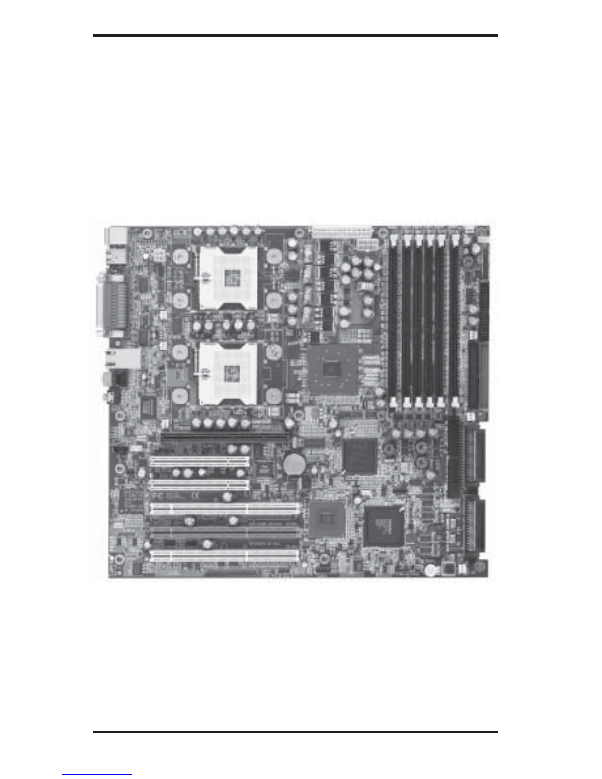
Figure 1-1. SUPER X5DA8 Image
Chapter 1: Introduction
1-5
Introduction
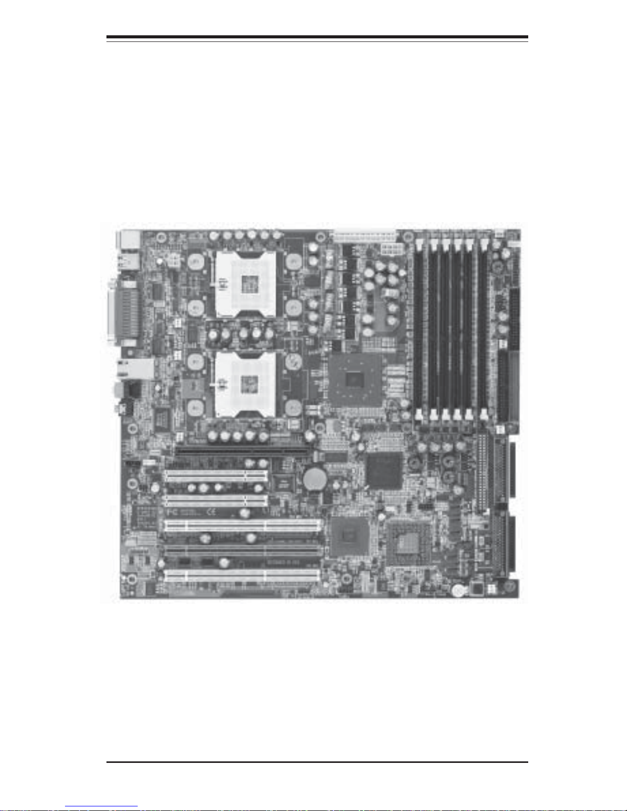
Figure 1-2. SUPER X5DAE Image
1-6
Introduction
SUPER X5DA8/X5DAE/X5DAL-G/X5DAL-TG2 User's Manual
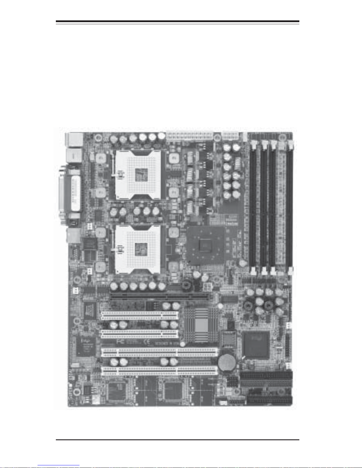
Figure 1-3. SUPER X5DAL-G Image
Chapter 1: Introduction
1-7
Introduction
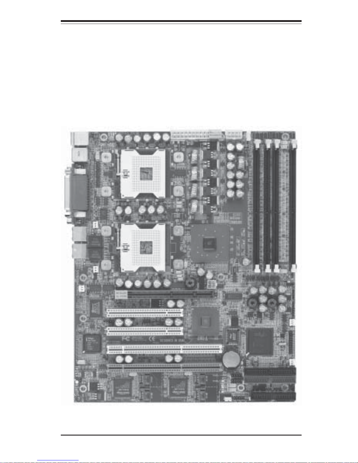
Figure 1-4. SUPER X5DAL-TG2 Image
1-8
Introduction
SUPER X5DA8/X5DAE/X5DAL-G/X5DAL-TG2 User's Manual
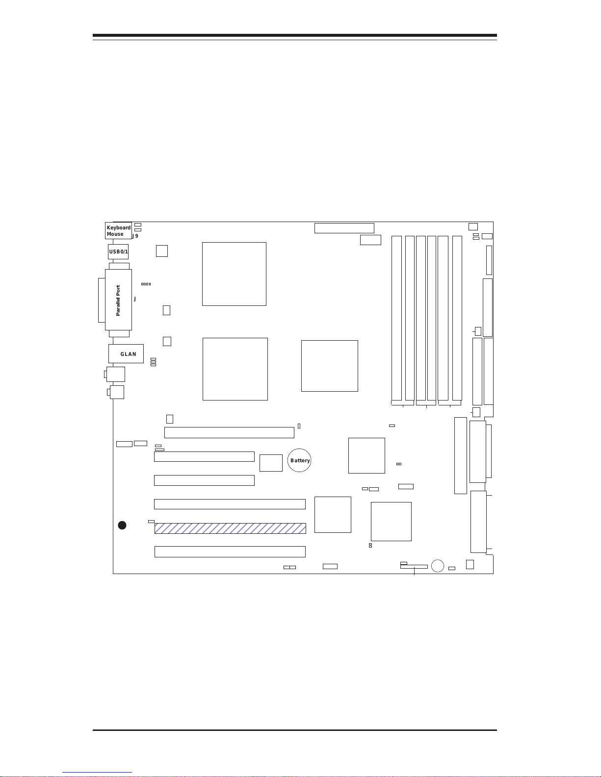
Figure 1-5. SUPER X5DA8 Layout
(not drawn to scale)
Jumpers not noted are for test purposes only.
Parallel Port
USB0/1
Keyboard
Mouse
J9
GLAN
Battery
J7
JPUSB
J30
JC1
JC2
CPU 2
CPU 1
Overheat Fan
CPU Fan1
CD1 CD2
CPU Fan2
33 MHz PCI #5
33 MHz PCI #4
133 MHz PCI-X #3
100 MHz PCI-X #2
100 MHz PCI-X #1
IDE #2
IDE #1
FLOPPY
Ultra III LVD SCSI CH A
BIOS
MCH
AIC-7902
ICH4
Speaker
8xAGP (1.5V)
COM1
COM2
ATX PWR CONN
J15
DIMM #1B
DIMM #1A
DIMM #2B
DIMM #2A
DIMM #3B
DIMM #3A
BANK 1 BANK 2
BANK 3
JF2
JP36
CPU1 Chassis Fan
JP9
JP8
JP7
J2J3
CPU2 Chassis Fan
Chassis Fan1
JA1
JA2
Ultra III LVD SCSI CH B
Chassis Fan2
JD4
J12
JP40
FPUSB 2/3
WOL
JWOR1
JP35
JD1: JPA1/PWR LED/SPEAKER
JPA2
FPUSB 0/1
JL1
S
UPER X5DA8
®
I/O BRIDGE
Ultra SCSI CH B (50-pin)
JA3
JP34
JP39
JP37
JP33
JP38
JOH1
JBT1
D1-D4
DA1
DA2
JPWAKE

Chapter 1: Introduction
1-9
Introduction
X5DA8 Quick Reference
Jumper Description Default Setting
JBT1 CMOS Clear See Chapter 2
JD4 GLAN Enable/Disable Pins 1-2 (Enabled)
JP9 Power Fail Alarm En/Disable Open (Disabled)
JP33 CPU Chassis/CPU Fan Select Closed (CPU Fan)
JP34 SCSI Enable/Disable Pins 1-2 (Enabled)
JP37 Watch Dog Pins 2-3 (NMI)
JP38 Thermal Fan Control See Chapter 2
JP39 System (Front Side) Bus Speed Pins 1-2 (Auto)
JP40 Onboard Audio Enable/Disable Pins 1-2 (Enabled)
JPA1/JPA2 SCSI CH A/B Termination Open (Enabled)
JPUSB USB Wake-up Pins 1-2 (Disabled)
JPWAKE Keyboard Wake-up Pins 1-2 (Disabled)
Connector Description
ATX PWR CONN Primary ATX Power Connector
CD1/CD2 Audio CD Input (large/small)
COM1/COM2 COM1/COM2 Serial Port Connector
CPU/CHS/OH FAN CPU/Chassis/Overheat Fan Headers
DIMM#1A-DIMM#3B Memory (RAM) Slots
FPUSB0/1/2/3 Front Panel USB Headers
GLAN G-bit Ethernet Port
J2/J3 IDE1/2 Hard Disk Drive Connector
J7 Parallel (Printer) Port
J9 PS/2 Keyboard/Mouse Ports
J12 IR/CIR Header
J15 Processor Power Connector
J30 Power Conn. (for use with AGP Pro cards)
JA1/JA2/JA3 Ultra320 LVD SCSI CH A/B/B Connector
JC1/JC2 MIC/LINE IN LINE OUT
JD1 PWR LED/Speaker Header
JF2 Front Control Panel Connector
JL1 Chassis Intrusion Header
JOH1 Overheat LED
JP7 Floppy Disk Drive Connector
JP8 Third Power Supply Fail Header
JP35 Keylock Switch Connector
JP36 Power Supply Fail Alarm Reset Switch
JWOR1 Wake-on-Ring Header
USB0/1 Universal Serial Bus Ports
WOL Wake-on-LAN Header
1-10
Introduction
SUPER X5DA8/X5DAE/X5DAL-G/X5DAL-TG2 User's Manual
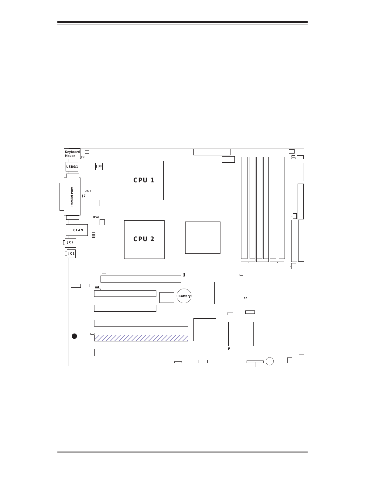
Figure 1-6. SUPER X5DAE Layout
(not drawn to scale)
Jumpers not noted are for test purposes only.
234567890123456789012
3
Parallel Port
USB0/1
Keyboard
Mouse
J9
GLAN
Battery
J7
J30
JC1
JC2
CPU 2
CPU 1
Overheat Fan
CPU Fan1
CD1 CD2
CPU Fan2
33 MHz PCI #5
33 MHz PCI #4
133 MHz PCI-X #3
100 MHz PCI-X #2
100 MHz PCI-X #1
IDE #2
IDE #1
FLOPPY
BIOS
MCH
AIC-7902
ICH4
Speaker
8xAGP (1.5V)
COM1
COM2
ATX PWR CONN
J15
DIMM #1B
DIMM #1A
DIMM #2B
DIMM #2A
DIMM #3B
DIMM #3A
BANK 1 BANK 2
BANK 3
JF2
JP36
CPU1 Chassis Fan
JP9
JP8
JP7
J2J3
CPU2 Chassis Fan
Chassis Fan1
Chassis Fan2
JD4
J12
JP40
FPUSB 2/3
WOL
JWOR1
JP35
JD1: PWR LED/SPEAKER
FPUSB 0/1
JL1
S
UPER X5DAE
®
I/O BRIDGE
JP39
JP37
JP33
JP38
JOH1
JBT1
DA1
DA2
D1-D4
JPUSB
JPWAKE

Chapter 1: Introduction
1-11
Introduction
X5DAE Quick Reference
Jumper Description Default Setting
JBT1 CMOS Clear See Chapter 2
JD4 GLAN Enable/Disable Pins 1-2 (Enabled)
JP9 Power Fail Alarm En/Disable Open (Disabled)
JP33 CPU Chassis/CPU Fan Select Closed (CPU Fan)
JP37 Watch Dog Pins 2-3 (NMI)
JP38 Thermal Fan Control See Chapter 2
JP39 System (Front Side) Bus Speed Pins 1-2 (Auto)
JP40 Onboard Audio Enable/Disable Pins 1-2 (Enabled)
JPUSB USB Wake-up Pins 1-2 (Disabled)
JPWAKE Keyboard Wake-up Pins 1-2 (Disabled)
Connector Description
ATX PWR CONN Primary ATX Power Connector
CD1/CD2 Audio CD Input (large/small)
COM1/COM2 COM1/COM2 Serial Port Connector
CPU/CHS/OH FAN CPU/Chassis/Overheat Fan Headers
DIMM#1A-DIMM#3B Memory (RAM) Slots
FPUSB0/1/2/3 Front Panel USB Headers
GLAN G-bit Ethernet Port
J2/J3 IDE1/2 Hard Disk Drive Connector
J7 Parallel (Printer) Port
J9 PS/2 Keyboard/Mouse Ports
J12 IR/CIR Header
J15 Processor Power Connector
J30 Power Conn. (for use with AGP Pro cards)
JC1/JC2 MIC/LINE IN LINE OUT
JD1 PWR LED/Speaker Header
JF2 Front Control Panel Connector
JL1 Chassis Intrusion Header
JOH1 Overheat LED
JP7 Floppy Disk Drive Connector
JP8 Third Power Supply Fail Header
JP35 Keylock Switch Connector
JP36 Power Supply Fail Alarm Reset Switch
JWOR1 Wake-on-Ring Header
USB0/1 Universal Serial Bus Ports
WOL Wake-on-LAN Header
1-12
Introduction
SUPER X5DA8/X5DAE/X5DAL-G/X5DAL-TG2 User's Manual
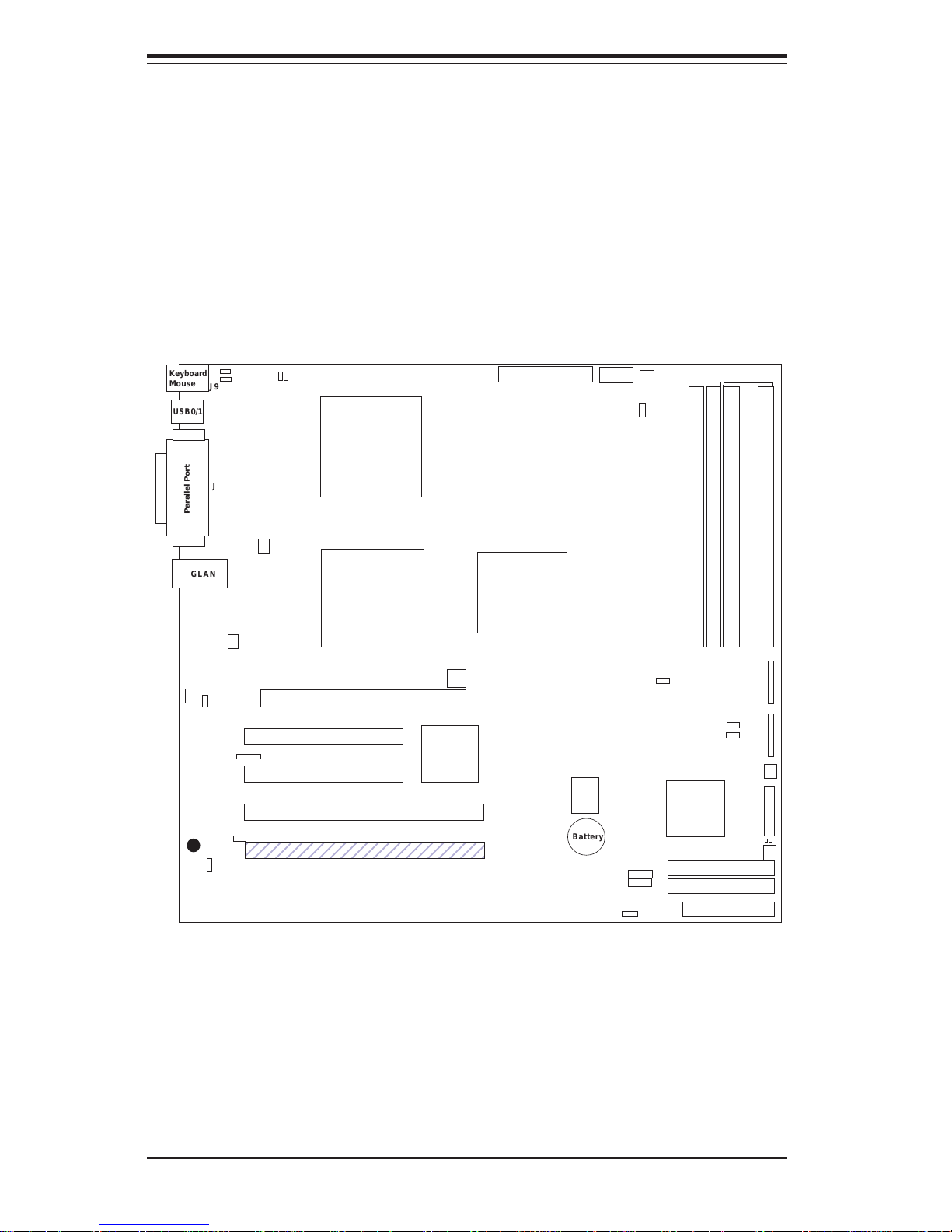
Figure 1-7. SUPER X5DAL-G Layout
(not drawn to scale)
Parallel Port
USB0/1
Keyboard
Mouse
J9
GLAN
Battery
J7
J30
CPU 2
CPU 1
Overheat Fan
CPU Fan1
CPU Fan2
33 MHz PCI #2
33 MHz PCI #1
100 MHz PCI-X #2
133 MHz PCI-X #1
IDE #2
IDE #1
FLOPPY
BIOS
MCH
ICH4
8xAGP (1.5V)
COM1
COM2
ATX PWR CONN
J15
DIMM #1
DIMM #2
DIMM #3
DIMM #4
BANK 0
BANK 1
Chassis Fan 1
JP9
JP8
JP7
J2
J3
FPUSB 2/3
WOL
JP35
JD1
FPUSB 0/1
JL1
S
UPER X5DAL-G
®
I/O BRIDGE
JP39
JBT1
JPUSB
JPWAKE
JP36/JOH1/JP37
JF2
Chassis Fan 2
JPL1
JP38
JWOR1
J12
D3, D4
Jumpers not noted are for test purposes only.

Chapter 1: Introduction
1-13
Introduction
X5DAL-G Quick Reference
Jumper Description Default Setting
JBT1 CMOS Clear See Chapter 2
JP9 Power Fail Alarm En/Disable Open (Disabled)
JP37 Watch Dog Pins 2-3 (NMI)
JP38 Thermal Fan Control See Chapter 2
JP39 System (Front Side) Bus Speed Pins 1-2 (Auto)
JPA1/JPA2 Serial ATA Enable/Disable Pins 1-2 (Enabled)
JPL1 GLAN Enable/Disable Pins 1-2 (Enabled)
JPUSB USB Wake-up Pins 1-2 (Disabled)
JPWAKE Keyboard Wake-up Pins 1-2 (Disabled)
Connector Description
ATX PWR CONN Primary ATX Power Connector
COM1/COM2 COM1/COM2 Serial Port Connector
CPU/CHS/OH FAN CPU/Chassis/Overheat Fan Headers
DIMM#1-DIMM#4 Memory (RAM) Slots
FPUSB0/1/2/3 Front Panel USB Headers
GLAN G-bit Ethernet Port
J2/J3 IDE1/2 Hard Disk Drive Connector
J7 Parallel (Printer) Port
J9 PS/2 Keyboard/Mouse Ports
J12 IR/CIR Header
J15 Processor Power Connector
J30 Power Conn. (for use with AGP Pro cards)
JD1 PWR LED/Speaker Header
JF2 Front Control Panel Connector
JL1 Chassis Intrusion Header
JOH1 Overheat LED
JP7 Floppy Disk Drive Connector
JP8 Third Power Supply Fail Header
JP35 Keylock Switch Connector
JP36 Power Supply Fail Alarm Reset Switch
JWOR1 Wake-on-Ring Header
USB0/1 Universal Serial Bus Ports
WOL1 Wake-on-LAN Header
1-14
Introduction
SUPER X5DA8/X5DAE/X5DAL-G/X5DAL-TG2 User's Manual
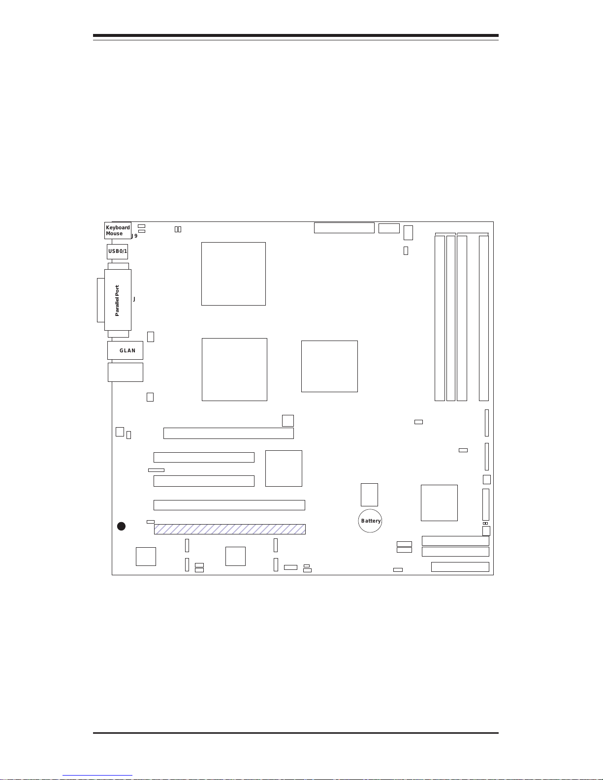
Figure 1-8. SUPER X5DAL-TG2 Layout
(not drawn to scale)
Parallel Port
USB0/1
Keyboard
Mouse
J9
GLAN
Battery
J7
J30
CPU 2
CPU 1
Overheat Fan
CPU Fan1
CPU Fan2
33 MHz PCI #2
33 MHz PCI #1
100 MHz PCI-X #2
66 MHz PCI #1
IDE #2
IDE #1
FLOPPY
BIOS
MCH
ICH4
8xAGP (1.5V)
COM1
COM2
ATX PWR CONN
J15
DIMM #1
DIMM #2
DIMM #3
DIMM #4
BANK 0
BANK 1
Chassis Fan 1
JP9
JP8
JP7
J2
J3
FPUSB 2/3
WOL
JD1
FPUSB 0/1
S
UPER X5DAL-TG2
®
I/O BRIDGE
JP39
JBT1
JPUSB
JPWAKE
JP36/JOH1/JP37
JF2
Chassis Fan 2
JPL1
JP38
JWOR1
J12
D3, D4
JPA1
JPA2
SATA#1
SATA#2
SATA#3
SATA#4
SATA
Cntrlr
JSLED
JL1
WOL1
GLAN
SATA
Cntrlr
Jumpers not noted are for test purposes only.

Chapter 1: Introduction
1-15
Introduction
X5DAL-TG2 Quick Reference
Jumper Description Default Setting
JBT1 CMOS Clear See Chapter 2
JP9 Power Fail Alarm En/Disable Open (Disabled)
JP37 Watch Dog Pins 2-3 (NMI)
JP38 Thermal Fan Control See Chapter 2
JP39 System (Front Side) Bus Speed Pins 1-2 (Auto)
JPA1 SATA #1/#2 Enable/Disable Pins 1-2 (Enabled)
JPA2 SATA #3/#4 Enable/Disable Pins 1-2 (Enabled)
JPL1 GLAN Enable/Disable Pins 1-2 (Enabled)
JPUSB USB Wake-up Pins 1-2 (Disabled)
JPWAKE Keyboard Wake-up Pins 1-2 (Disabled)
Connector Description
ATX PWR CONN Primary ATX Power Connector
COM1/COM2 COM1/COM2 Serial Port Connector
CPU/CHS/OH FAN CPU/Chassis/Overheat Fan Headers
DIMM#1-DIMM#4 Memory (RAM) Slots
FPUSB0/1/2/3 Front Panel USB Headers
GLAN G-bit Ethernet Port
J2/J3 IDE1/2 Hard Disk Drive Connector
J7 Parallel (Printer) Port
J9 PS/2 Keyboard/Mouse Ports
J12 IR/CIR Header
J15 Processor Power Connector
J30 Power Conn. (for use with AGP Pro cards)
JD1 PWR LED/Speaker Header
JF2 Front Control Panel Connector
JL1 Chassis Intrusion Header
JOH1 Overheat LED
JP7 Floppy Disk Drive Connector
JP8 Third Power Supply Fail Header
JP35 Keylock Switch Connector
JP36 Power Supply Fail Alarm Reset Switch
JSLED Serial ATA Drive Activity
JWOR1 Wake-on-Ring Header
USB0/1 Universal Serial Bus Ports
WOL1 Wake-on-LAN Header

1-16
Introduction
SUPER X5DA8/X5DAE/X5DAL-G/X5DAL-TG2 User's Manual
Motherboard Features
CPU
• Single or dual Intel® 604/603-pin XeonTM processors of up to 3.20 GHz at a
533/400 MHz front side (system) bus speed.
Note: Please refer to the support section of our web site for a complete listing of
supported processors (http://www.supermicro.com/TechSupport.htm).
Memory
• X5DA8/X5DAE: Six 184-pin DIMM sockets supporting up to 12 GB of
registered ECC DDR-266/200 (PC2100/1600) SDRAM
• X5DAL-G/X5DAL-TG2: Four 184-pin DIMM sockets supporting up to 8
GB of registered ECC or unbuffered ECC DDR-266/200 (PC2100/1600)
SDRAM
Note: Interleaved memory; requires memory modules to be installed in pairs. See Section 2-3
for details.
Chipset
• Intel E7505 chipset
Expansion Slots
• X5DA8/X5DAE X5DAL-G/X5DAL-TG2
One 64-bit, 133 MHz PCI-X One 64-bit, 133 MHz PCI-X*
Two 64-bit, 100 MHz PCI-X One 64-bit, 100 MHz PCI-X
Two 32-bit, 33 MHz PCI Two 32-bit, 33 MHz PCI
One 8xAGP Pro (1.5V) One 8xAGP Pro (1.5V)
* This is a 64-bit, 66 MHz PCI slot on the X5DAL-TG2.
BIOS
• 4 Mb Phoenix® Flash ROM
• APM 1.2, DMI 2.1, PCI 2.2, ACPI 1.0, Plug and Play (PnP), SMBIOS 2.3
PC Health Monitoring
• Onboard voltage monitors for CPU cores, chipset voltage, 3.3V, +5V,
+12V and 3.3V standby
• Fan status monitor with firmware/software on/off control
• CPU/chassis temperature monitors
• Environmental temperature monitor and control
• CPU fan auto-off in sleep mode
• CPU slow-down on temperature overheat

Chapter 1: Introduction
1-17
Introduction
• CPU overheat LED header
• Power-up mode control for recovery from AC power loss
• Auto-switching voltage regulator for CPU core
• System overheat LED and control
• Chassis intrusion detection
• System resource alert
ACPI Features (optional)
• Microsoft OnNow
• Slow blinking LED for suspend state indicator
• Main switch override mechanism
Onboard I/O
• AIC-7902 for dual channel Ultra320 SCSI (X5DA8)
• Zero channel SCSI RAID support (green slot, X5DA8)
• Support for up to four Serial ATA hard drives (X5DAL-TG2)
• Zero channel Serial ATA RAID support (green slot, X5DAL-TG2)
• Intel 82545EM Gb Ethernet controller
• Intel EW82546EB dual Gb Ethernet controller (X5DAL-TG2)
• 2 EIDE Ultra DMA/100 bus master interfaces
• 1 floppy port interface (up to 2.88 MB)
• 2 Fast UART 16550A compatible serial ports
• 1 EPP/ECP Parallel Port
• PS/2 mouse and PS/2 keyboard ports
• Up to 6 USB 2.0 (Universal Serial Bus) ports
• AC'97 Audio CODEC (not on X5DAL-G, X5DAL-TG2)
Other
• Internal/external modem ring-on
• Wake-on-LAN (WOL)
• Console redirection
CD/Diskette Utilities
• BIOS flash upgrade utility and device drivers
Dimensions
• X5DA8: Extended ATX, 12" x 13.05" (304.8 x 331.5 mm)
• X5DAE: Extended ATX, 12" x 13.05" (304.8 x 331.5 mm)
• X5DAL-G/X5DAL-TG2: ATX, 12" x 9.8" (304.8 x 249 mm)
1-18
Introduction
SUPER X5DA8/X5DAE/X5DAL-G/X5DAL-TG2 User's Manual
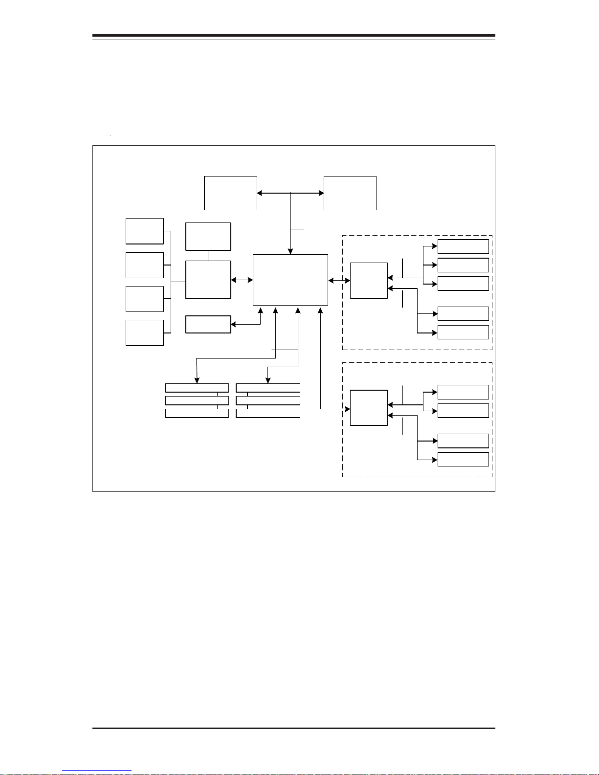
MCH
533/400 MHz System Bus
266/200 MHz Memory Bus
ATA 100
Ports
P64H2
Processor 2 Processor 1
2-Channel
DDR SDRAM
ICH4
USB 2.0
Ports
SMBus
Super IO
33 MHz PC I
8xAGP
PCI-X #1
PCI-X #2
SCSI
PCI-X #3
GLAN
100 MH z P CI-X Bus
100 MH z P CI-X Bus
P64H2
PCI-X #1
Serial ATA
PCI-X #2
GLAN
133/66 (DAL-G/DA L-TG2) MH z
PCI-X/PCI Bus
100 MH z P CI-X Bus
X5DA8/X5DAE
X5DAL-G/X5DAL-TG2
SATA for X5DAL-TG2 only
PCI #1 on X5DAL-TG2
Figure 1-9. Intel E7505 Chipset:
System Block Diagram
Note: This is a general block diagram. Please see the previous Motherboard
Features pages for details on the features of each motherboard.

Chapter 1: Introduction
1-19
Introduction
1-2 Chipset Overview
The Intel E7505 chipset is a high-performance chipset with a performance
and feature-set designed dual processor servers. The E7505 chipset consists of three major components: the Memory Controller Hub (MCH), the I/O
Controller Hub 4 (ICH4) and the PCI-X 64-bit Hub 2.0 (P64H2).
The MCH has four hub interfaces, one to communicate with the ICH4 and
three for high-speed I/O communications. The MCH employs a 144-bit wide
memory bus for a DDR-266 memory interface, which provides a total bandwidth of 4.27 GB/s. The ICH4 interface is a 266 MB/sec point-to-point
connection using an 8-bit wide, 66 MHz base clock at a 4x data transfer
rate. The P64H2 interface is a 1 GB/s point-to-point connection using a 16bit wide, 66 MHz base clock at an 8x data transfer rate.
The ICH4 I/O Controller Hub provides various integrated functions, including
a two-channel Ultra ATA/100 bus master IDE controller, USB 2.0 host controllers, an integrated LAN controller, a System Management Bus controller
and an AC'97 compliant interface.
The P64H2 PCI-X Hub provides a 16-bit connection to the MCH for highperformance IO capability and two independent 64-bit PCI-X interfaces.
1-3 Special Features
BIOS Recovery
The BIOS Recovery function allows you to recover your BIOS image file if
the BIOS flashing procedure fails (see Section 3-3).
Recovery from AC Power Loss
BIOS provides a setting for you to determine how the system will respond
when AC power is lost and then restored to the system. You can choose
for the system to remain powered off (in which case you must hit the
power switch to turn it back on) or for it to automatically return to a poweron state. See the Power Lost Control setting in the Advanced BIOS Setup
section (Peripheral Device Configuration) to change this setting. The default setting is Always On.

1-20
Introduction
SUPER X5DA8/X5DAE/X5DAL-G/X5DAL-TG2 User's Manual
1-4 PC Health Monitoring
This section describes the PC health monitoring features of the SUPER
X5DA8/X5DAE/X5DAL-G/X5DAL-TG2. All have an onboard System Hardware Monitor chip that supports PC health monitoring.
Onboard Voltage Monitors for the CPU Cores, Chipset
Voltage, +3.3V, +5V, +12V and +3.3V Standby
An onboard voltage monitor will scan these voltages continuously. Once a
voltage becomes unstable, a warning is given or an error message is sent
to the screen. Users can adjust the voltage thresholds to define the
sensitivity of the voltage monitor.
Fan Status Monitor with Firmware/Software On/Off Control
The PC health monitor can check the RPM status of the cooling fans. The
onboard 3-pin CPU and chassis fans are controlled by the power management functions. The thermal fan is controlled by the overheat detection
logic.
Environmental Temperature Control
The thermal control sensor monitors the CPU temperature in real time and
will turn on the thermal control fan whenever the CPU temperature exceeds
a user-defined threshold. The overheat circuitry runs independently from
the CPU. It can continue to monitor for overheat conditions even when the
CPU is in sleep mode. Once it detects that the CPU temperature is too high,
it will automatically turn on the thermal control fan to prevent any overheat
damage to the CPU. The onboard chassis thermal circuitry can monitor the
overall system temperature and alert users when the chassis temperature
is too high.
CPU Fan Auto-Off in Sleep Mode
The CPU fan activates when the power is turned on. It continues to operate
when the system enters Standby mode. When in sleep mode, the CPU will
not run at full power, thereby generating less heat.

Chapter 1: Introduction
1-21
Introduction
CPU Overheat LED and Control
This feature is available when the user enables the CPU overheat warning
function in the BIOS. This allows the user to define an overheat temperature. When this temperature is exceeded, both the overheat fan and the
warning LED are triggered.
System Resource Alert
This feature is available when used with Intel's LANDesk Client Manager
(optional). LDCM is used to notify the user of certain system events. For
example, if the system is running low on virtual memory and there is insufficient hard drive space for saving the data, you can be alerted of the
potential problem.
Auto-Switching Voltage Regulator for the CPU Core
The auto-switching voltage regulator for the CPU core can support up to
20A current and auto-sense voltage IDs ranging from 1.4V to 3.5V. This
will allow the regulator to run cooler and thus make the system more stable.
1-5 ACPI Features
ACPI stands for Advanced Configuration and Power Interface. The ACPI
specification defines a flexible and abstract hardware interface that provides a standard way to integrate power management features throughout
a PC system, including its hardware, operating system and application software. This enables the system to automatically turn on and off peripherals
such as CD-ROMs, network cards, hard disk drives and printers. This also
includes consumer devices connected to the PC such as VCRs, TVs, telephones and stereos.
In addition to enabling operating system-directed power management, ACPI
provides a generic system event mechanism for Plug and Play and an operating system-independent interface for configuration control. ACPI leverages the Plug and Play BIOS data structures while providing a processor
architecture-independent implementation that is compatible with both Windows 2000 and Windows NT 5.0.

1-22
Introduction
SUPER X5DA8/X5DAE/X5DAL-G/X5DAL-TG2 User's Manual
Microsoft OnNow
The OnNow design initiative is a comprehensive, system-wide approach to
system and device power control. OnNow is a term for a PC that is always
on but appears to be off and responds immediately to user or other requests.
Slow Blinking LED for Suspend-State Indicator
When the CPU goes into a suspend state, the chassis power LED will start
blinking to indicate that the CPU is in suspend mode. When the user presses
any key, the CPU will wake-up and the LED will automatically stop blinking
and remain on.
Main Switch Override Mechanism
When an ATX power supply is used, the power button can function as a
system suspend button to make the system enter a SoftOff state. The
monitor will be suspended and the hard drive will spin down. Depressing
the power button again will cause the whole system to wake-up. During
the SoftOff state, the ATX power supply provides power to keep the required circuitry in the system alive. In case the system malfunctions and
you want to turn off the power, just depress and hold the power button for
4 seconds. This option can be set in the Power section of the BIOS Setup
routine.
External Modem Ring-On
Wake-up events can be triggered by a device such as the external modem
ringing when the system is in the SoftOff state. Note that external modem
ring-on can only be used with an ATX 2.01 (or above) compliant power
supply.
Wake-On-LAN (WOL)
Wake-On-LAN is defined as the ability of a management application to remotely power up a computer that is powered off. Remote PC setup, updates and asset tracking can occur after hours and on weekends so that
daily LAN traffic is kept to a minimum and users are not interrupted. The
motherboards have a 3-pin header (WOL) to connect to the 3-pin header on
 Loading...