

Page 1

SUPER
®
Dual Pentium Pro Processor
®
SUPER P6DNF
Single Pentium Pro Processor
SUPER P6SNF
USER’S MANUAL
®
Revision 2.1
Page 2

The information in this User’s Manual has been carefully reviewed and is believed to be
accurate. The vendor assumes no responsibility for any inaccuracies that may be
contained in this document, makes no commitment to update or to keep current the
information in this manual, or to notify any person or organization of the updates.
SUPER P6DNF/P6SNF reserves the right to make changes to the product described in this
manual at any time and without notice. This product, including software, if any, and
documentation may not, in whole or in part, be copied, photocopied, reproduced, translated
or reduced to any medium or machine without prior written consent.
IN NO EVENT WILL SUPER P6DNF/P6SNF BE LIABLE FOR DIRECT, INDIRECT,
SPECIAL, INCIDENTAL, OR CONSEQUENTIAL DAMAGES ARISING FROM THE USE OR
INABILITY TO USE THIS PRODUCT OR DOCUMENTATION, EVEN IF ADVISED OF THE
POSSIBILITY OF SUCH DAMAGES. IN PARTICULAR, THE VENDOR SHALL NOT HAVE
LIABILITY FOR ANY HARDWARE, SOFTWARE, OR DATA STORED OR USED WITH THE
PRODUCT, INCLUDING THE COSTS OF THE REPAIRING, REPLACING, OR
RECOVERING SUCH HARDWARE, SOFTWARE, OR DATA.
Copyright © 1996 by SUPER P6DNF/P6SNF
All rights reserved.
Printed in the United States of America.
Unless you request and receive written permission from SUPER P6DNF/P6SNF, you may
not copy any part of this document.
Intel i386 and Pentium Pro are trademarks and Intel is a registered trademark of Intel Corporation.
AMI is a trademark of American Megatrend, Inc. Novell is a registered trademark of
Novell, Inc. SUPER P6DNF/P6SNF is a trademark of SUPER P6DNF/P6SNF. UNIX is
a registered trademark of UNIX Systems Laboratories. Windows, Windows NT and Windows 95 are trademarks and Microsoft, MS-DOS and XENIX are registered trademarks of
Microsoft Corporation. AT, IBM, OS/2 and PS/2 are registered trademarks of International
Business Machines Corporation.
All products and company names not mentioned above are trademarks or registered
trademarks of their respective holders.
Do not upgrade the BIOS unless you are notified to do so. Please call technical
support first before upgrading the boot-block BIOS.
Baud Rate: 1200-14400 bps, Data Bits: 8, Stop Bit: 1, Parity: None
SUPER BBS # (408) 451-1114 (24 hours)
Page 3

Preface
About This Manual
This manual is written for system houses, PC technicians and
knowledgeable PC end users. It provides information for the installation and use of the SUPER™ P6DNF/P6SNF motherboard, which
supports the 200/180/166/150 and >200 MHz Intel® Pentium® Pro
processors.
The Pentium Pro processor has two 64-bit data buses. One bus
interconnects to the built-in L2 cache and the other is an external
bus that interconnects with the system memory, I/O and the other
processor. Both come with ECC (Error Checking and Correction)
allowing for the correction of single-bit data errors and detection of
2-bit errors on the data bus.
Manual Organization
Chapter 1, Introduction, describes the features, specifications and
performance of the SUPER P6DNF/P6SNF system board, provides
detailed information about the chipset, and offers warranty information.
Refer to Chapter 2, Installation, for a list of the equipment needed
for a system based on the SUPER P6DNF/P6SNF system board.
This chapter provides you with the instructions for handling staticsensitive devices, checking and/or configuring the jumpers. Read
this chapter when you want to install or remove SIMM memory modules and to mount the system board in the chassis. Also refer to
this chapter to connect the floppy and hard disk drives, IDE interface, parallel port, serial ports, as well as the cables for the power
supply, reset cable, Keylock/Power LED, speaker and keyboard.
iii
Page 4

SUPER P6DNF/P6SNF User's Manual
If you encounter any problem, please see Chapter 3, Troubleshooting, which describes troubleshooting procedures for video, memory, and the setup configuration stored in memory. Instructions are
also included on contacting a technical assistance support representative and returning merchandise for service and the BBS# for
BIOS upgrades .
iv
Page 5

Preface
Table of Contents
Preface
About This Manual ......................................................................................... iii
Manual Organization...................................................................................... iii
Chapter 1:
1-1 Overview............................................................................................... 1-1
SUPER P6DNF Motherboard Layout........................................ 1-4
SUPER P6SNF Motherboard Layout ........................................ 1-5
SUPER P6DNF/P6SNF System Board Architecture.............. 1-6
Features......................................................................................... 1-7
1-2 Power Supply ...................................................................................... 1-9
1-3 Chipset Overview................................................................................ 1-9
1-4 National Semiconductor 87306 ..................................................... 1-10
1-5 Voltage Regulator Modules ............................................................ 1-10
1-6 System Overheat Thermal Control ................................................1-11
1-7 Warranty, Technical Support, and Service .................................. 1-12
Parts.............................................................................................. 1-12
BIOS .............................................................................................. 1-12
Labor............................................................................................. 1-12
Returns......................................................................................... 1-12
Chapter 2: Installation
2-1 SUPER P6DNF/P6SNF System Components.............................. 2-1
Standard System Configuration ................................................ 2-1
Enhanced System Configuration .............................................. 2-2
2-2 Static-Sensitive Devices ................................................................... 2-2
Precautions ................................................................................... 2-2
Unpacking...................................................................................... 2-3
2-3 Configuring System Board Jumpers.............................................. 2-3
v
Page 6

Manufacturing Settings ............................................................... 2-3
Changing the CPU Speed ......................................................... 2-4
2-4 Mounting the Motherboard in the Chassis ................................... 2-4
2-5 Connecting Cables ............................................................................ 2-4
Power Supply Connectors.......................................................... 2-5
Turbo Function.............................................................................. 2-5
Reset Cable Connector .............................................................. 2-7
Keylock/Power LED Cable Connector ..................................... 2-7
Keyboard Connector .................................................................... 2-8
Thermal Control Connector ....................................................... 2-8
Hard Drive LED ............................................................................ 2-9
Speaker Cable Connector.......................................................... 2-9
PS/2 Keyboard and Mouse Ports ........................................... 2-10
Serial Ports.................................................................................. 2-10
Back-up Cooling Fan and Buzzer Connectors ..................... 2-11
2-6 Installing/Removing the SIMM Modules ...................................... 2-12
SIMM Module Installation .......................................................... 2-12
Removing SIMM Modules ......................................................... 2-13
2-7 Connecting Floppy and Hard Disk Drives .................................. 2-14
Parallel Port Connector ............................................................ 2-15
Floppy Connector ....................................................................... 2-16
IDE Interfaces ............................................................................. 2-17
Chapter 3: Troubleshooting
3-1 Troubleshooting Procedures ........................................................... 3-1
No Video ........................................................................................ 3-1
Troubleshooting Flowchart ........................................................ 3-2
Memory Error ................................................................................. 3-3
Losing the System’s Setup Configuration.............................. 3-3
3-2 Technical Support Procedures........................................................ 3-4
3-3 Returning Merchandise for Service................................................ 3-4
vi
Page 7

Table of Contents
vii
Page 8

SUPER P6DNF/P6SNF User's Manual
viii
Page 9

Chapter 1: Introduction
Chapter 1
Introduction
1-1 Overview
SUPER™ P6DNF/P6SNF is a high performance, function-enhanced
computer system board based on Intel® Pentium® Pro 200/180/166/
150 MHz processors. SUPER P6DNF/P6SNF incorporates Intel
440FX chipset. It supports dual processing (SUPER P6DNF) and
FPM or EDO memory of up to 1GB.
The Pentium Pro processor is Intel’s top-of-the-line generation of
performance for servers, workstations, and high-end desktops. It
delivers its superior performance through its Dynamic Execution
microarchitecture which allows multiple branch prediction, dataflow
analysis and speculative execution.
The Pentium Pro processor includes 16KB of internal cache and an
integrated 256KB or 512KB non-blocking secondary cache in the
same package. Having the L2 cache inside the package will not
only save space, it will also have the CPU core communicating with
the L2 cache at full speed. Non-blocking means that the transactions on the processor bus do not block subsequent bus transactions. For example, when a cache miss occurs, the processor will
continue to process other instructions while initiating a bus transaction to satisfy the cache miss. These instructions could generate
additional cache misses which could cause more bus transactions.
The Pentium Pro processor can maintain up to four concurrent requests of the bus.
The general purpose registers of the Pentium Pro processor are
the same as on previous generations. The processor bus achieves
high bus efficiency by providing support for multiple, pipelined
transactions and deferred replies. A single processor may have up
to 4 outstanding transactions at the same time. There are a variety
1-1
Page 10

SUPER P6DNF/P6SNF User’s Manual
of wider datapaths both inside and outside the chip. It has an
external 64-bit bus in order to communicate more efficiently with the
system memory. The package have two cavities with about 21 million transistors. The larger one is the CPU core with 5.5 million
transistors. The smaller one is the non-blocking cache which contains 15.5 million transistors.
Peripheral Component Interconnect (PCI) provides industry-leading
performance and compatibility. The 32-bit, 33 MHz pathway to the
CPU offers performance unmatched by other bus architectures. The
PCI standard is clearly defined to ensure complete compatibility. A
PCI add-on card available today will work in any PC-compliant system in the future. The PCI add-on card interface is processor independent. This will enable an efficient transition to future processor
generations and use with multiple processor architecture.
In addition to the security of a true standard, PCI add-on cards feature auto-configurability for easy integration. The user-friendly BIOS
automatically allocates system resources for add-on cards and configures hard disk, memory, and other peripherals. No more
hassles with settings, jumpers, or switches. Just plug in the card
and go (Plug and Play or PnP).
The motherboard’s four 32-bit slots with industry standard PCI design have a very high performance capability that provides an ideal
system board solution for a wide range of demanding applications;
such as networking multiuser environments, computer aided
design (CAD), computer aided manufacturing (CAM), computeraided engineering (CAE), database management, desktop publishing, image processing, and artificial intelligence. The
motherboard’s additional four ISA slots provide standard 16-bit
compatibility for AT-type add-on card expansion.
1-2
Page 11

Chapter 1: Introduction
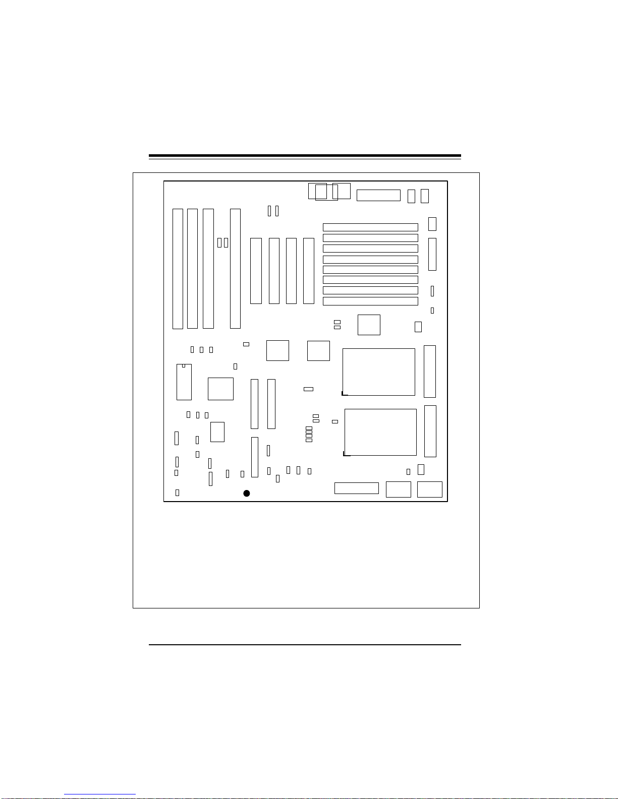
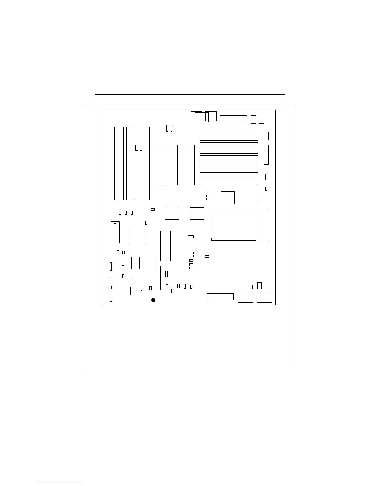
Figure 1-1 shows the layout of the SUPER P6DNF motherboard.
Figure 1-2 shows the layout of the SUPER P6SNF motherboard.
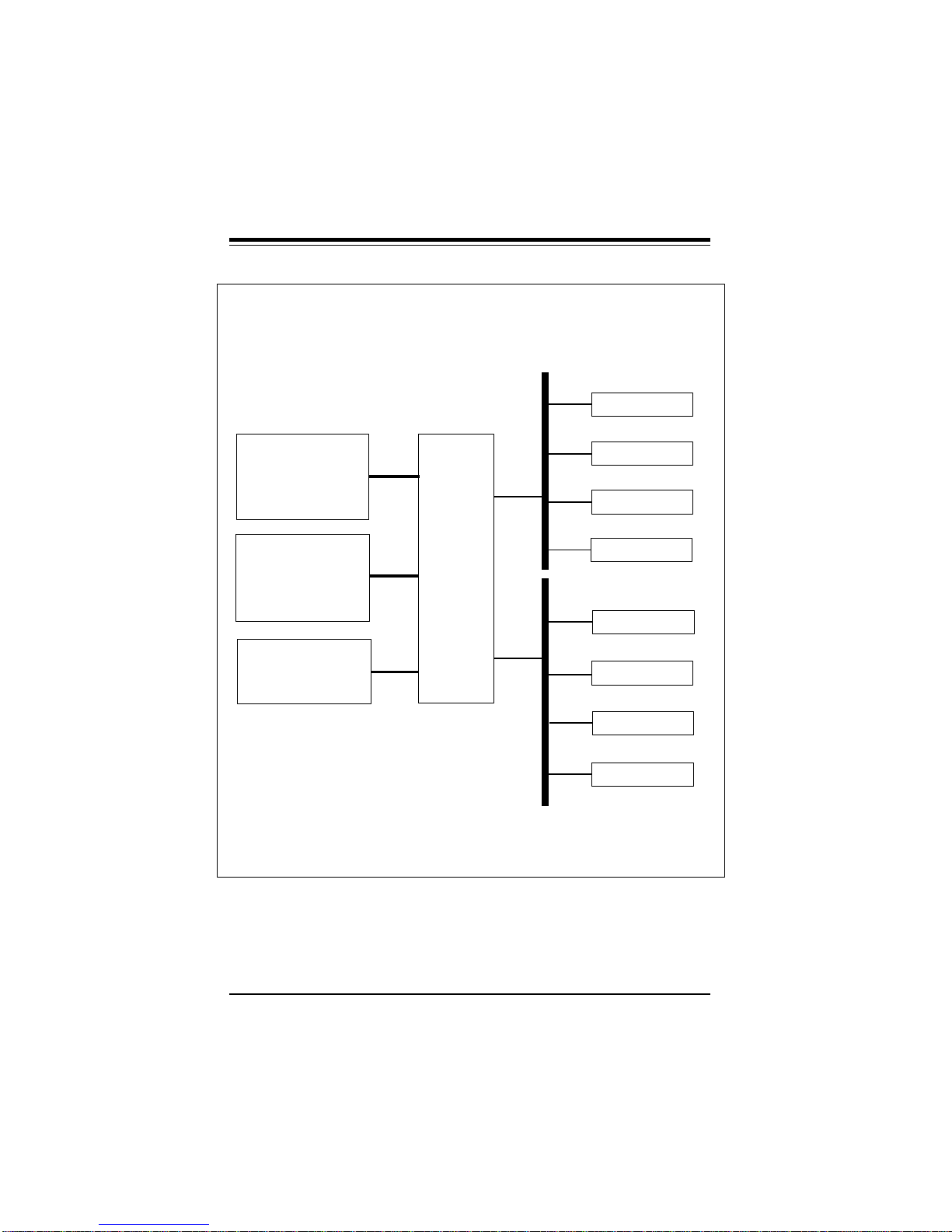
Figure 1-3 shows the architecture of the SUPER P6DNF/P6SNF
motherboard.
1-3
Page 12
SUPER P6DNF/P6SNF User’s Manual
J28 J31 J29
U834
JP20
KEYLOCK
1
J22
SPEAKER
1
1
JP21
RESET
1
BIOS
J829
1
JP39
SMI SW
1 1
JP880
J828
1
1
JP38
1
JP96
IR CON
J32
J88 J86
11
J832 J833 J831
1
J830
1
U831
J827
1
BT1
BATTERY
+
JP97
1
JP89
ALARM
JP88
1
1
SUPER
JP42
1
J37 J38
J12 J11
1
IDE 2
J85
1
HD LED
FLOPPY
JP95
®
P6DNF
1 1
USB2
1
1
1
J23
J35 J36
U13
IDE 1
JP91
1
USB1
JP921 JP93
J20
5V POWER
Bank3
Bank3
Bank2
Bank2
Bank1
Bank1
Bank0
Bank0
U6
U33
J39
J82
PS/2
MOUSE
J40
J81 AT KB
U5
J83
PS/2 KB
1
JP27
1
JP26
CPU 1
JP15
1
JP36
JP37
1
1
1
1
1
1
JP32
JP31
JP30
JP29
JP90
1
U34
1
JP13
1
1
CPU 2
1
J21
3V POWER
J818
1
JP23
COM1
JP35
JP34
J824
1
VRM
1
VRM
2
COM2
J84
PS/2
MOUSE
1
J817
1
PARALLEL
JP881
Ext Battery
JP22
1
11
VR4VR3
——–——— Manufacturer Settings ——–——
J86: 1-2 JP15: 2-3
J88: 1-2 JP26: OFF
J827: 1-2 JP27: ON
J828 1-2 JP38: OFF
J829: 1-2 JP88: OFF
JP13: 2-3
JP880: 1-2 (default)
2-3 CMOS Clear
JP42: ON (ISA CLK=PCI CLK/4)
OFF (ISA CLK=PCI CLK/3)
——–———————–————––——–——–—
Figure 1-1. SUPER P6DNF Motherboard Layout
—–—–—–——CPU Speed—––—–————
150 166 180 200
JP29 OFF OFF ON ON
JP30 ON ON OFF OFF
JP31 ON ON ON ON
JP32 ON ON ON ON
JP36 ON OFF ON OFF
JP37 OFF ON OFF ON
——–—–——————————–—————
1-4
Page 13
Chapter 1: Introduction
J28 J31 J29
U834
JP20
KEYLOCK
1
J22
SPEAKER
1
1
JP21
RESET
1
J88 J86
11
J832 J833 J831
1 1
1
J828
1
JP880
1
JP38
1
JP96
IR CON
J827
1
JP97
1
U831
BT1
+
JP89
ALARM
1
1
BIOS
J829
1
JP39
SMI SW
SUPER P6SNF
J32
J830
1
BATTERY
JP88
JP42
1
J37 J38
J12 J11
1
IDE 2
J85
1
HD LED
FLOPPY
JP95
®
1 1
USB2
1
1
1
J23
J35 J36
U13
IDE 1
JP91
1
USB1
JP921 JP93
1
J39
J82
PS/2
MOUSE
J40
JP15
1
JP36
JP37
1
1
1
1
1
J81 AT KB
U5
JP32
JP31
JP30
JP29
JP90
J20
5V POWER
J83
PS/2 KB
Bank3
Bank3
Bank2
Bank2
Bank1
Bank1
Bank0
Bank0
U6
1
JP27
1
JP26
U33
CPU 1
1
1
JP13
1
1
J21
3V POWER
J818
1
JP23
COM1
JP35
JP34
J824
COM2
1
JP881
Ext Battery
1
VRM
1
J84
PS/2
MOUSE
1
J817
1
PARALLEL
JP22
11
VR4VR3
——–——— Manufacturer Settings ——–——
J86: 1-2 JP15: 2-3
J88: 1-2 JP26: OFF
J827: 1-2 JP27: ON
J828 1-2 JP38: OFF
J829: 1-2 JP88: OFF
JP13: 2-3
JP880: 1-2 (default)
2-3 CMOS Clear
JP42: ON (ISA CLK=PCI CLK/4)
OFF (ISA CLK=PCI CLK/3)
——–———————–————––——–——–—
Figure 1-2. SUPER P6SNF Motherboard Layout
—–—–—–——CPU Speed—––—–————
150 166 180 200
JP29 OFF OFF ON ON
JP30 ON ON OFF OFF
JP31 ON ON ON ON
JP32 ON ON ON ON
JP36 ON OFF ON OFF
JP37 OFF ON OFF ON
——–—–——————————–—————
1-5
Page 14
SUPER P6DNF/P6SNF User’s Manual
PCI
Bus
PCI
CPU 1
with 256/512KB
L2 cache
CPU 2 (P6DNF)
with 256/512KB
L2 cache
1 GB DRAM
FPM or EDO
Intel
440FX
Chipset
PCI
PCI
PCI
ISA
ISA
ISA
ISA
ISA
Bus
Figure 1-3. P6DNF/P6SNF System Board Architecture
1-6
Page 15

Chapter 1: Introduction
Features
The following list covers the general features of the SUPER P6DNF/
P6SNF motherboard.
CPU
• (SUPER P6DNF) Dual Pentium Pro 200/180/166/150 and >200
MHz processors with integrated 256 or 512KB non-blocking
secondary cache
• (SUPER P6SNF) Single Pentium Pro 200/180/166/150 and >200
MHz processors with integrated 256 or 512KB non-blocking
secondary cache
• 16KB internal cache
• 387-pin ZIF (Zero Insertion Force) socket 8
Bus Speed
• 66/60 MHz external bus with 64-bit data plus 8 bits ECC
Memory
• 64-bit wide data bus of up to 1GB
• Supports 1 MB, 2 MB, 4 MB, 8MB, 16MB and 32MB (x32 or x36
60ns, 72-pin) Fast Page DRAM or EDO
• Error Checking and Correction and Parity Checking support
Dimensions
• Full AT size
• 13.8" x 12"
IDE support
• Integrated IDE controller provides two IDE interfaces for hard
disk(s) and/or CD ROM(s)
• Supports Mode 4
Super I/O
• Supports EPP (Enhanced Parallel Port) and ECP (Extended
Capabilities Port) parallel port, floppy interface and 2 Fast
UART 16550 serial ports
1-7
Page 16

SUPER P6DNF/P6SNF User’s Manual
Expansion
• Four 16-bit ISA slots
• Four 32-bit PCI slots
BIOS
• AMI® Flash BIOS with built-in setup
• Plug and Play (PnP) with boot block support
Software Compatibility
• 100% IBM® PC/AT® compatible
• DOS, OS/2, SCO UNIX® Open Server, XENIX®, Novell® SMP,
Windows™, Windows NT™ and Windows™ 95
Testing
• 50°C, 48-hour, dynamic burn-in with system-level testing
Manufacturing and Support
• Made in U.S.A.
• Design-level Technical Support and Service in U.S.A.
1-8
Page 17

Chapter 1: Introduction
1-2 Power Supply
As with all computer products, a stable power source is necessary
for proper and reliable operation. It is even more important for high
CPU clock rates like 200, 180, 166, 150 MHz and future Pentium
Pro processors for the SUPER P6DNF/P6SNF system board.
The SUPER P6DNF/P6SNF can accomodate 5V power supplies.
Although most power supplies generally meet the specifications required by the CPU, some power supplies are not adequate. To
obtain the highest system reliability, be certain that your power supply provides +5 VDC with a voltage range between +4.95 VDC (minimum) and +5.25 VDC (maximum).
It is highly recommended that you use a high quality power supply.
Additionally, in areas where noisy power transmission is present,
you may choose to install a line filter to separate noise from the
computer. You can also install a power surge protector to help
avoid problems caused by power surges.
1-3 Chipset Overview
The Intel 440FX chipset is a high-performance PCIset that supports
full symmetric multi-processor protocol for up to two processors. It
is compliant to the PCI Rev. 2.1 specification. The memory controller provides capability for auto-detection of EDO/FPM DRAM type
installed in the system. It also provides data integrity features including ECC in the memory array and parity error detection. Memory
is upgradable up to 1GB for the SUPER P6DNF/P6SNF.
1-9
Page 18

SUPER P6DNF/P6SNF User’s Manual
1-4 National Semiconductor Super I/O Controller
The National Semiconductor 87306 Super I/O Controller incorporates an IDE control logic, two full function serial ports, an IEEE
1284 parallel port, industry standard floppy disk controller with 16
byte FIFO, Real Time Clock and an 8042 compatible keyboard controller all in one chip.
The IDE interfaces provide up to Mode 4 support. The two serial
ports are software compatible with the Fast UART 16550. The parallel port is EPP (Enhanced Parallel Port) and ECP (Extended Capabilities Port) compatible, including level 2 support. It includes a
protection circuit against damage caused when the printer is powered up. EPP mode provides for greater throughput than Compatible or Extended modes by supporting faster transfer rates and a
mechanism that allows the host to address peripheral device registers directly. Faster transfers are achieved by automatically generating the address and data strobes. EPP is compatible with both
Compatible and Extended mode parallel-port devices.
1-5 Voltage Regulator Modules (VRM)
The Voltage Regulator Module (VRM1 and VRM2) is a DC-to-DC
converter with a standardized interface to the system. The standardization allows a variety of Voltage Regulator Modules to support
the Pentium Pro processor family and to provide a cost effective
support for CPU upgrade.
1-10
Page 19

Chapter 1: Introduction
1-6 System Overheat Thermal Control
A back-up cooling fan can be hooked up to JP91, JP92 or JP93. If
the power supply fan or the processor cooling fan goes down, the
circuitry will detect an overheat temperature depending on the user
setting. It will then trigger the backup cooling fan or alarm. The
alarm can be turned on or off using JP88. JP90 is used to connect
the overheat LED. The user can set the temperature range using
JP95. A buzzer can also be connected on JP89 that will sound off
that it is time to replace the power supply fan or the CPU cooling
fan. It is important that the back-up cooling fan be installed correctly in such a way that it will not only cool down the processor but
the whole system as well.
1-11
Page 20

SUPER P6DNF/P6SNF User’s Manual
1-7 Warranty, Technical Support, and Service
The manufacturer will repair or exchange any unit or parts free of
charge due to manufacturing defects for one year (12 months) from
the original invoice date of purchase.
Parts
Defective parts will be exchanged or repaired within one year (12
months) from the manufacturer’s original invoice purchase date.
BIOS
The manufacturer will exchange the BIOS free of charge (shipping
and handling excluded) due to existing incompatibility issues within
one year from the manufacturer’s original invoice purchase date.
Labor
Mail-in or carry-in service is available for one year (12 months) from
the manufacturer’s original invoice purchase date.
Returns
If you must return products for any reason, refer to Chapter 3 in this
manual, “Returning Merchandise for Service.”
1-12
Page 21

Chapter 2: Installation
Chapter 2
Installation
2-1 SUPER P6DNF/P6SNF System Components
The equipment listed in this section is required to build a high performance system based on the SUPER P6DNF/P6SNF motherboard. The minimum configuration for a standard system is listed
below. To create the full enhanced configuration, add the enhanced
system configuration equipment listed on the next page to the
equipment listed below.
Standard System Configuration
• 300 watt (minimum) 5V power supply for SUPER P6DNF
• 250 watt (minimum) 5V power supply for SUPER P6SNF
• Chassis with a speaker connected to a 4-pin connector, a push
button switch with 2-pin connector for the reset function, and a
keylock connected to a 5-pin connector
• SUPER P6DNF/P6SNF system board
• AT-compatible keyboard (84 or 101 style keyboard)
• 8 MB or 16 MB of system memory
• One 1.2 MB 5.25" and/or one 1.44 MB 3.5" floppy disk drive
• Use PCI Fast SCSI card and hard disk drive or the on-board
IDE interface
• PCI VGA card
2-1
Page 22

SUPER P6DNF/P6SNF User’s Manual
Enhanced System Configuration
• Tape drive (for backups)
• Sound card
• Modem/FAX card
• CD-ROM drive
• Add SIMM modules for 32 MB, 64 MB, or 128 MB of system
memory
• Use one or two PCI Ultra Wide Fast SCSI cards
• Use up to four PCI Fast Network cards
2-2 Static-Sensitive Devices
Static-sensitive electric discharge can damage electronic components. To prevent damage to your system board, it is important
to handle it very carefully. The following measures are generally
sufficient to protect your equipment from static discharge.
Precautions
• Use a grounded wrist strap designed for static discharge.
• Touch a grounded metal object before you remove the board
from the anti-static bag.
• Handle the board by its edges only; do not touch its
components, peripheral chips, memory modules, or gold
contacts.
• When handling chips or modules, avoid touching their pins.
• Put the system board and peripherals back into their anti-static
bags when not in use.
• Be sure your computer system’s chassis allows excellent
conductive contacts between its power supply, case, mounting
fasteners, and the system board for grounding purposes.
2-2
Page 23

Chapter 2: Installation
Unpacking
The system board is shipped in anti-static packaging to avoid static
damage. When unpacking the board, be sure the person handling
the board is static-protected.
2-3 Configuring System Board Jumpers
Use the following settings to configure your system board. Refer to
Figure 1-1 or Figure 1-2 for an illustration of the jumpers. Manufacturing jumpers are permanently fixed or preset in place on the system board. You cannot move them. These jumpers are labeled on
the system board and are listed below as Manufacturer Settings.
Manufacturer Settings
J86: 1-2
J88: 1-2
J827: 1-2
J828 1-2
J829: 1-2
JP13: 2-3
JP15: 2-3
JP26: OFF
JP27: ON
JP38: OFF
JP88: OFF
JP880: 1-2 Default
2-3 CMOS Clear
JP42: ON (ISA CLK=PCI CLK/4)
OFF (ISA CLK=PCI CLK/3)
2-3
Page 24

SUPER P6DNF/P6SNF User’s Manual
Changing the CPU Speed
The SUPER P6DNF/P6SNF motherboard supports Intel Pentium
Pro 200/180/166/150 MHz and future Pentium Pro processors. For
SUPER P6DNF, both CPU1 and CPU2 have to be the same speed.
To change the CPU speed, change the jumpers shown below on
Table 2-1:
Table 2-1. CPU Speed Selection
150 166 180 200
JP29 OFF OFF ON ON
JP30 ON ON OFF OFF
JP31 ON ON ON ON
JP32 ON ON ON ON
JP36 ON OFF ON OFF
JP37 OFF ON OFF ON
2-4 Mounting the Motherboard in the Chassis
The motherboard has eight standard mounting holes to fit all different types of chassis. Chassis may come with a variety of mounting
fasteners, made of metal or plastic. Although a chassis may have
both metal and plastic fasteners, metal fasteners are the most
highly recommended because they ground the system board to the
chassis. Therefore, use as many metal fasteners as possible for
better grounding.
®
2-5 Connecting Cables
After you have securely mounted the motherboard to the chassis,
you are ready to connect the cables.
2-4
Page 25

Chapter 2: Installation
Table 2-2. 5V Power Supply Connector Pin Definitions
Connector Pin
Number Number Function
J20 1 Power Good (Power on reset, TTL signal)
2 +5 VCC
3 +12 VCC
4 -12 VCC
5 Ground (Black wire to be connected)
6 Ground (Black wire to be connected)
7 Ground (Black wire to be connected)
8 Ground (Black wire to be connected)
9 -5 VCC
10 +5 VCC
11 +5 VCC
12 +5 VCC
Power Supply Connectors
Attach power supply cables to J20 for a 5V power supply or J21 for
a 3.3V power supply (optional for OEM customers only). Do not
force the cables, but make sure they are fully seated. The two black
wires on each power cable sit next to each other when correctly
installed. See Table 2-2 for pin definitions of a 5V power supply.
See Table 2-3 for pin definitions of a 3.3V power supply.
Turbo Function
There are no jumpers for turbo switch and turbo LED. By default,
SUPER P6DNF/P6SNF is in turbo mode.
2-5
Page 26

SUPER P6DNF/P6SNF User’s Manual
Table 2-3. 3.3V Power Supply Connector Pin Definitions
(Optional for OEM customers only)
Connector Pin
Number Number Function
J21 1 Ground (Black wire to be connected)
2 Ground (Black wire to be connected)
3 Ground (Black wire to be connected)
4 +3.3 VCC
5 +3.3 VCC
6 +3.3 VCC
7 +3.3 VCC
8 +3.3 VCC
9 +3.3 VCC
10 Ground (Black wire to be connected)
11 Ground (Black wire to be connected)
12 Ground (Black wire to be connected)
Note:
The +3.3V power supply is for 3.3V PCI add-on cards or CPU power
support when 3.3V CPU is used.
2-6
Page 27

Chapter 2: Installation
Reset Cable Connector
The reset cable connector JP21 has two pins. The
connector attaches to the hardware Reset switch on the computer
case. See Table 2-4 for pin definitions
Table 2-4. Reset Pin Definitions
Pin
Number Definition
1 Reset
2 Ground
Keylock/Power LED Cable Connector
The keylock/power LED cable connector JP20 has five pins. See
Table 2-5 for pin definitions.
Table 2-5. Keylock/Power LED Pin Definitions
Pin
Number Function Definition
1 + Red wire, LED power
2 Key No connection
3 GND Black wire
4 Keyboard inhibit
5 GND Black wire
2-7
Page 28

SUPER P6DNF/P6SNF User’s Manual
Keyboard Connector
The keyboard connector J81 has five pins. See Table 2-6 for pin
definitions.
Table 2-6. Keyboard Connector Pin Definitions
Pin
Number Function
1 Keyboard clock
2 Keyboard data
3 Spare
4 Ground
5 +5 VDC
Thermal Control Connector
Use the settings on Table 2-7 to set the system temperature condition for JP95. Once the temperature cools down, the back-up fan
will automatically shut down.
Table 2-7. Thermal Control Connector
Setting Turn on (°°C) Shut down (°°C)
1-2 55 51
2-3 62 58
OFF 69 65
2-8
Page 29

Chapter 2: Installation
Hard Drive LED
The hard drive LED J23 has four pins. See Table 2-8 for pin definitions.
Table 2-8. Hard Drive LED Pin Definitions
Pin
Number Function
1 Pull_Up_330
2 Key
3 HD Active
4 Pull_Up_330
Speaker Cable Connector
The speaker cable connector J22 has four pins. See Table 2-9 for
pin definitions.
Table 2-9. Speaker Connector Pin Definitions
Pin
Number Function Definition
1 + Red wire, speaker data
2 Key No connection
3 VCC Speaker data
4 GND Black wire
2-9
Page 30

SUPER P6DNF/P6SNF User’s Manual
PS/2 Keyboard and Mouse Ports
The PS/2 keyboard is located on J83 and the PS/2 mouse is located
on J82 and J84. The cable for J84 can be obtained from the manufacturer. See Table 2-10 for pin definitions.
Table 2-10. PS/2 Keyboard and Mouse Pin Definitions
(J82 and J83 Optional for OEM customers only)
Pin
Number Function
1 Data
2 NC
3 Ground
4 VCC
5 Clock
6 NC
Serial Ports
Serial port COM1 is located on J818 and serial port COM2 is
located on J824. See Table 2-11 for pin definitions.
Table 2-11. Serial Ports Pin Definitions
Pin Pin
Number Function Number Function
1 DCD 6 CTS
2 DSR 7 DTR
3 Serial In 8 RI
4 RTS 9 GND
5 Serial Out 10 NC
2-10
Page 31

Chapter 2: Installation
Back-up Cooling Fan and Buzzer Connectors*
Connect the back-up cooling fan to JP91, JP92 or JP93 and the
buzzer to JP89. See Table 2-12 for pin definitions.
Table 2-12. Back-up Cooling Fan and Buzzer Connectors
Pin Definition
Number
1 +12 V
2 GND
* Caution: These connectors are DC direct.
2-11
Page 32

SUPER P6DNF/P6SNF User’s Manual
2-6 Installing/Removing the SIMM Modules
SUPER P6DNF/P6SNF can accommodate a maximum of 1 GB of
on-board memory, using standard 72-pin SIMM memory modules.
You can use any 1 MB, 2 MB, 4 MB, 8MB, 16MB or 32MB Fast Page
Mode or EDO SIMM modules. You can use 32-bit or 36-bit
memories.
There are no jumpers to configure the on-board memory. Two slots
of memory totaling 8 MB are required for a minimum system configuration. Memory banks must contain two 72-pin single-sided or
double-sided SIMM modules. Memory timing requires 60ns fast
page devices.
Refer to Figure 2-1 and the instructions below for installing or removing SIMM modules.
CAUTION
Exercise extreme care when installing or removing the
SIMM modules to prevent any possible damages.
SIMM Module Installation
1. Insert SIMM modules in Bank 0 through Bank 3 as required
for the desired system memory.
2. Insert each SIMM module into its socket at an angle away
from the CPU sockets. The component side of the SIMM
modules must face the CPU sockets.
3. Gently press the SIMM module in the direction of the CPU
sockets until it snaps upright into place in the socket.
2-12
Page 33

Chapter 2: Installation
To Remove:
Use your thumb to gently push the edge of
the socket and release the module. Do this
on both sides for each module.
To Install:
Insert at an
angle, then
snap upright
into place.
SIMM
Figure 2-1. Installing/Removing a SIMM Memory Module
Removing SIMM Modules
1. Remove SIMM modules in correct descending order — from
Bank 3 through Bank 0.
2. Gently push the edge of the sockets to the side to release the
module. Remove one side of the SIMM module first, and then
the other side, to prevent breaking the socket.
2-13
Page 34

SUPER P6DNF/P6SNF User’s Manual
2-7 Connecting Parallel, Floppy and Hard Disk
Drives
Use the following information to connect the floppy and hard disk
drive cables.
• The floppy disk drive cable has seven twisted wires.
• A red mark on a wire typically designates the location of pin 1.
• A single floppy disk drive ribbon cable has 34 wires and two
connectors to provide for two floppy disk drives. The connector
with twisted wires always connects to drive A, and the connector
that does not have the twisted wires always connects to drive B.
• An IDE hard disk drive requires a data ribbon cable with 40 wires,
and a SCSI hard disk drive requires a SCSI ribbon cable with 50
wires.
• A single IDE hard disk drive cable has two connectors to provide
for two drives. To select an IDE disk drive as C, you would normally set the drive select jumper on the drive to DS1. To select
an IDE disk drive as D, you would normally set the drive select
jumper on the drive to DS2. Consult the documentation that
came with your disk drive for details on actual jumper locations
and settings.
• A single SCSI ribbon cable typically has three connectors to provide for two hard disk drives and the SCSI adapter. (Note: most
SCSI hard drives are single-ended SCSI devices.) The SCSI ID
is determined by jumpers or a switch on the SCSI device. The
last internal (and external) SCSI device cabled to the SCSI
adapter must be terminated.
• Some drives require a special controller card. Read your disk
drive manual for details.
2-14
Page 35

Chapter 2: Installation
Parallel Port Connector
The parallel port is located on J817. See Table 2-13 for pin definitions.
Table 2-13. Parallel Port Pin Definitions
Pin Pin
Number Function Number Function
1 Strobe- 2 Auto Feed 3 Data Bit 0 4 Error 5 Data Bit 1 6 Init 7 Data Bit 2 8 SLCT IN 9 Data Bit 3 10 GND
11 Data Bit 4 12 GND
13 Data Bit 5 14 GND
15 Data Bit 6 16 GND
17 Data Bit 7 18 GND
19 ACJ- 20 GND
21 BUSY 22 GND
23 PE 24 GND
25 SLCT 26 NC
2-15
Page 36

SUPER P6DNF/P6SNF User’s Manual
Floppy Connector
The floppy connector is located on J85. See Table 2-14 for pin
definitions.
Table 2-14. Floppy Connector Pin Definitions
Pin Pin
Number Function Number Function
1 GND 2 FDHDIN
3 GND 4 Reserved
5 Key 6 FDEDIN
7 GND 8 Index9 GND 10 Motor Enable
11 GND 12 Drive Select B13 GND 14 Drive Select A15 GND 16 Motor Enable
17 GND 18 DIR19 GND 20 STEP21 GND 22 Write Data23 GND 24 Write Gate25 GND 26 Track 0027 GND 28 Write Protect29 GND 30 Read Data31 GND 32 Side 1 Select33 GND 34 Diskette
2-16
Page 37

Chapter 2: Installation
IDE Interfaces
There are no jumpers to configure the on-board IDE interfaces J11
and J12. Refer to Table 2-15 for the pin definitions.
Table 2-15. IDE Connector Pin Definitions
Pin Pin
Number Function Number Function
1 Reset IDE 2 GND
3 Host Data 7 4 Host Data 8
5 Host Data 6 6 Host Data 9
7 Host Data 5 8 Host Data 10
9 Host Data 4 10 Host Data 11
11 Host Data 3 12 Host Data 12
13 Host Data 2 14 Host Data 13
15 Host Data 1 16 Host Data 14
17 Host Data 0 18 Host Data 15
19 GND 20 Key
21 DRQ3 22 GND
23 I/O Write- 24 GND
25 I/O Read- 26 GND
27 IOCHRDY 28 BALE
29 DACK3- 30 GND
31 IRQ14 32 IOCS1633 Addr 1 34 GND
35 Addr 0 36 Addr 2
37 Chip Select 0 38 Chip Select 139 Activity 40 GND
2-17
Page 38

SUPER P6DNF/P6SNF User’s Manual
2-18
Page 39

Chapter 3: Troubleshooting
Chapter 3
Troubleshooting
3-1 Troubleshooting Procedures
Use the following procedures to troubleshoot your system. If you
have followed all of the procedures below and still need assistance,
refer to the ‘Technical Support Procedures’ and/or ‘Returning
Merchandise for Service’ section(s) in this chapter.
No Video
Use the following steps for troubleshooting your system
configuration.
1. If you have no video, follow the flowchart in Figure 3-1
3-1
Page 40

SUPER P6DNF/P6SNF User’s Manual
Power
N
On-board
LED on?
Display?
Power
Supply OK?
N
Replace
Y
Power
Supply
Speaker
Beeps?
Check Memory
Y
Speaker
Beeps?
Check CPU & BIOS
On
Video
Y
N
N
N
Y
System
Hold?
Y
Check BIOS
Setting & Add-on
Card
Y
Number
of Beeps
Memory Problem:
Check Memory
0
N
Motherboard
Good
8
Video Card
Problem
Y
Speaker
Beeps?
N
Replace
Motherboard
Figure 3-1. Troubleshooting Flowchart
2. Check for missing jumpers or improper installation of the
ROM BIOS.
3. Make sure the video card and its jumper setting (as
appropriate) match the monitor type.
4. Ensure that all peripheral cards are properly installed in their
slots.
5. Use the speaker to determine if any beep codes exist. Refer
to Appendix C of the AMI BIOS Reference Manual for details
about beep codes.
3-2
Page 41

Chapter 3: Troubleshooting
NOTE
If you are a system integrator, VAR or OEM, a POST
diagnostics card is recommended for port 80h codes.
Refer to Appendix D.
Memory Error
If you encounter memory error, follow the procedures below.
1. Check to determine if SIMM modules are improperly installed.
2. Make sure that different types of SIMMs have not been
installed in different banks (e.g., a mixture of 2MB x 36 and 1
MB x 36 SIMMs in Banks 0).
3. Determine if different speeds of SIMMs have been installed in
the same or different banks, and the BIOS setup is configured
for the fastest speed of RAM used. It is recommended to use
the same RAM speed for SIMMs in different banks.
4. Check for bad SIMM modules or chips.
Losing the System’s Setup Configuration
1. Ensure that you are using a high quality power supply. A poor
quality power supply may cause the system to lose CMOS
setup. Refer to Chapter 1 of this manual for details.
2. If the above step does not fix the Setup Configuration
problem, contact your vendor for repair.
3-3
Page 42

SUPER P6DNF/P6SNF User’s Manual
3-2 Technical Support Procedures
1. Go through the ‘Troubleshooting Procedures’ section in this
chapter of the manual before calling Technical Support.
2. BIOS upgrades can be downloaded from the SUPER BBS#
(408) 451-1114, 24 hours a day, using 1200-14400 baud, 8
data bits, 1 stop bit and no parity.
Note: Not all BIOS can be flashed depending on the modifications on the boot block code.
3. If you still cannot get the problem resolved, have the following
information ready before you call for technical support:
• BIOS release date/version
• System board serial number
• Product model name
• Invoice number and date
• System configuration
3-3 Returning Merchandise for Service
A receipt or copy of your invoice marked with the date of purchase is
required before any warranty service will be rendered. You can
obtain service by calling your vendor for a Returned Merchandise
Authorization (RMA) number. When returning to the manufacturer,
the RMA number should be prominently displayed on the outside of
the shipping carton, and mailed prepaid or hand-carried. Shipping
and handling charges will be applied for all orders that must be
mailed when service is complete.
This warranty only covers normal consumer use and does not cover
damages incurred in shipping or from failure due to the alternation,
misuse, abuse, or improper maintenance of products.
During the warranty period, contact your distributor first for any
product problems.
3-4
Page 43

Chapter 3: Troubleshooting
3-5
Page 44

SUPER P6DNF/P6SNF User’s Manual
3-6
Page 45

Appendix A: Technical Specifications
Appendix A
Technical Specifications
A-1 System Specifications
Features
The following list covers the general features of the SUPER P6DOF/
P6SOF motherboard.
CPU
• Dual Pentium Pro 200/180/166/150 and >200 MHz processors
with integrated 256 or 512KB non-blocking secondary cache
• 16KB internal cache
• Dual 387-pin ZIF (Zero Insertion Force) socket 8
Bus Speed
• 66/60 MHz external bus with 64-bit data plus 8 bits ECC
Memory
• 64-bit wide data bus with 4-way interleaved memory of up to
1GB
• Supports 1 MB x 36, 2 MB x 36, 4 MB x 36, 8MB x 36, 16MB x 36
and 32MB x 36 (60ns or 70ns, 72-pin) Fast Page DRAM
• Error Checking and Correction and Parity Checking support
Dimensions
• Full AT size
• 13.8" x 12"
IDE support
• Integrated IDE controller provides an IDE interface for hard
disk(s) and/or CD ROM(s)
• Supports Type F IDE DMA
Super I/O
• Supports EPP (Enhanced Parallel Port) and ECP (Extended
Capabilities Port) parallel port, floppy interface and 2 Fast
UART 16550 serial ports
A-1
Page 46

SUPER P6DOF/P6SOF User’s Manual
Turbo/Non-turbo Function
• BIOS turbo speed selectable by the keyboard
(<Ctrl>+<Alt>+<Shift> and <+> or <->)
Expansion
• Four 16-bit ISA slots
• Four 32-bit PCI slots
BIOS
• AMI® BIOS with built-in setup
• Flash BIOS for better upgradability in the future
• Advanced Power Management (APM) Green PC Function
• Plug and Play (PnP) with boot block support
Shadowed/Cached BIOS
• Shadowed system/video BIOS
• Cached system/video BIOS
Software Compatibility
• 100% IBM® PC/AT® compatible
• DOS, OS/2, UNIX®, XENIX®, Novell®, Windows™, Windows NT™
and Windows™ 95
Testing
• 50°C, 48-hour, dynamic burn-in with system-level testing
Manufacturing and Support
• Made in U.S.A.
• Design-level Technical Support and Service in U.S.A.
A-2
Page 47

Appendix A: Technical Specifications
A-2 Memory Address Map
Table A-1. Memory Address Map
Address (Hex) Function
0000000–009FFFF 640 KB
00C0000–00DFFFF 128 KB
00F0000–00FFFFF 64 KB System ROM BIOS
0100000–0FDFFFF 15232 KB
0FF0000–0FFFFFF 64 KB
0000000–3FFFFFF 64 MB Extended memory
0000000–7FFFFFF 128 MB Total memory space addressable by SUPER
Video RAM display buffer
System ROM BIOS expansion
Duplicates of System ROM BIOS expansion at
0E0000–0EFFFF
Extended memory
A-3
Page 48

SUPER P6DOF/P6SOF User’s Manual
A-3 I/O Address Map
Table A-2. I/O Address Map
Address Function
0000-000F SIO - DMA 1
0020-0021 SIO - Interrupt Controller 1
0040-0043 SIO - Timer 1
0048-004B SIO - Timer 2
0060 Keyboard Controller Data Byte
0061 SIO - NMI, speaker control
0064 Keyboard Controller, CMD/STAT
0070, bit 7 SIO - Enable NMI
0070, bits SIO - Real Time Clock
0071 SIO - Real Time Clock, Data
0073 Reserved
0075 Reserved
0078 SIO - BIOS Timer
0080-008F SIO - DMA Page Register
00A0-00A1 SIO - Interrupt Controller 2
00C0-00DE SIO - DMA 2
00F0 Reset Numeric Error
0170-0177 Secondary IDE Channel
01F0-01F7 Primary IDE Channel
0278-027B Parallel Port 2
02F8-02FF On-Board Serial Port 2
0376 Secondary IDE Channel
0377 Secondary IDE Channel
0378-037F Parallel Port 1
03BC-03BF Parallel Port x
03E8-03EF Serial Port 3
03F0-03F5 Floppy Channel 1
03F6 Primary IDE Channel
03F7 (Write) Floppy Channel 1
03F7, bit 7 Floppy Disk Change
03F7, bits 6-0 Primary IDE Channel
03F8-03FF On-Board Serial Port 1
LPT + 400h ECP Port, LPT + 400h
0CF8 PCI Configuration
0CF9 Deturbo Mode Enable
C000-C0FF 82437FX Config
C200-C2FF 82237FB Config
A-4
Page 49

Appendix A: Technical Specifications
A-4 I/O Expansion Slots
Input/output direction is determined from the system board’s viewpoint. ‘I’ is input from the I/O bus to the system board. ‘O’ is output
from the system board to the I/O bus.
Ground GND B1 A1 -I/O CH CK I
O RESET DRV B2 A2 SD7 I/O
Power +5 VDC B3 A3 SD6 I/O
I IRQ9 B4 A4 SD5 I/O
Power -5 VDC B5 A5 SD4 I/O
I DRQ2 B6 A6 SD3 I/O
Power -12 VDC B7 A7 SD2 I/O
Ground GND B10 A10 -I/O CHRDY I
O -SMEMW B11 A11 AEN O
O -SMEMR B12 A12 SA19 I/O
I/O -IOW B13 A13 SA18 I/O
I/O -IOR B14 A14 SA17 I/O
O -DACK3 B15 A15 SA16 I/O
I DRQ3 B16 A16 SA15 I/O
O -DACK1 B17 A17 SA14 I/O
I DRQ1 B18 A18 SA13 I/O
I/O -REFRESH B19 A19 SA12 I/O
O CLK B20 A20 SA11 I/O
I IRQ7 B21 A21 SA10 I/O
I IRQ6 B22 A22 SA9 I/O
I IRQ5 B23 A23 SA8 I/O
I IRQ4 B24 A24 SA7 I/O
I IRQ3 B25 A25 SA6 I/O
O -DACK2 B26 A26 SA5 I/O
O T/C B27 A27 SA4 I/O
O BALE B28 A28 SA3 I/O
Power +5 VDC B29 A29 SA2 I/O
O OSC B30 A30 SA1 I/O
Ground GND B31 A31 SA0 I/O
I -MEMCS16 D1 C1 -BHE I/O
I -I/OCS16 D2 C2 LA23 I/O
I IRQ10 D3 C3 LA22 I/O
I IRQ11 D4 C4 LA21 I/O
I IRQ12 D5 C5 LA20 I/O
I IRQ15 D6 C6 LA19 I/O
I IRQ14 D7 C7 LA18 I/O
O -DACK0 D8 C8 LA17 I/O
I DRQ0 D9 C9 -MEMR I/O
O -DACK5 D10 C10 -MEMW I/O
I DRQ5 D11 C11 SD08 I/O
O -DACK6 D12 C12 SD09 I/O
I DRQ6 D13 C13 SD10 I/O
O -DACK7 D14 C14 SD11 I/O
I DRQ7 D15 C15 SD12 I/O
Power +5 VDC D16 C16 SD13 I/O
I -MASTER D17 C17 SD14 I/O
Ground GND D18 C18 SD15 I/O
A-5
Page 50

SUPER P6DOF/P6SOF User’s Manual
A-5 Peripheral Controller
Details for the Peripheral Controller Direct
Memory Address (DMA) channels, controller registers, page register
addresses, interrupts, timers/counters, and CMOS RAM address
map are given below.
Table A-3. DMA Channels
Channel Function
0 Spare (8-bit, 64 KB block transfer)
1 SDLC (8-bit, 64 KB block transfer)
2 Floppy Disk (8-bit, 64 KB block transfer)
3 Spare (8-bit, 64 KB block transfer)
4 Cascade for DMA controller 1
5 Spare (16-bit, 128 KB block transfer)
6 Spare (16-bit, 128 KB block transfer)
7 Spare (16-bit, 128 KB block transfer)
Table A-4. DMA Controller Registers
Address (Hex) Command Code
C0 CH-0 base and current address
C2 CH-0 base and current word count
C4 CH-1 base and current address
C6 CH-1 base and current word count
C8 CH-2 base and current address
CA CH-2 base and current word count
CC CH-3 base and current address
CE CH-3 base and current word count
D0 Read Status Register/Write Command Register
D2 Write Request Register
D4 Write Single Mask Register Bit
D6 Write Mode Register
D8 Clear Byte Pointer Flip-Flop
DA Read Temporary Register/Write Master Clear
DC Clear Master Register
DE Write All Mask Register Bits
A-6
Page 51

Appendix A: Technical Specifications
Table A-5. Page Register Addresses
Page Register I/O Address (Hex)
DMA Channel 0 87
DMA Channel 1 83
DMA Channel 2 81
DMA Channel 3 82
DMA Channel 5 8B
DMA Channel 6 89
DMA Channel 7 8A
Refresh 8F
Table A-6. Interrupt Controller
Level Function
NMI System memory parity error or I/O channel check
IRQ0 System timer 0 output
IRQ1 Keyboard output buffer full
IRQ2 Interrupt from controller 2 (levels 8-15)
IRQ3 Serial port 2
IRQ4 Serial port 1
IRQ5 Parallel port 2
IRQ6 Floppy disk controller
IRQ7 Parallel port 1
IRQ8 Real-time clock
IRQ9 Reserved
IRQ10 Reserved
IRQ11 Reserved
IRQ12 Reserved
IRQ13 Coprocessor interrupt
IRQ14 Hard disk controller
IRQ15 Reserved
A-7
Page 52

SUPER P6DOF/P6SOF User’s Manual
Table A-7. Timers/Counters
Channel Function Status
0 System Timer
Gate 0: Always Enabled
Clock In 0: 1.19 MHz clock
Clock Out 0: IRQ0
1 Memory Refresh Request/Generator
Gate 1: Always Enabled
Clock In 1: 1.19 MHz clock
Clock Out 1: Refresh request cycle
2 Speaker Tone Generator
Gate 2: Bit 0 of I/O port 61 H
Clock In 2: 1.19 MHz
Clock Out 2: Audio frequency to speaker
Table A-8. CMOS RAM Address Map
Address (Hex) Description
00 – 0D* Real-time clock:
Hex Decimal Function
0 0 Seconds
1 1 Second alarm
2 2 Minutes
3 3 Minute alarm
4 4 Hours
5 5 Hour alarm
6 6 Day of week
7 7 Date of month
8 8 Month
9 9 Year
A 10 Status Register A
B 11 Status Register B
C 12 Status Register C
D 13 Status Register D
* This byte is not included in the checksum calculation and is not part of
the configuration record.
A-8
Page 53

Appendix A: Technical Specifications
Table A-8. CMOS RAM Address Map (Continued)
Address (Hex) Description
0E* Diagnostic status byte
0F* Shutdown status byte
10 Floppy disk drive type byte
11 Reserved
12 Disk type byte, for drives C and D, types 1-14
13 Reserved
14 Equipment byte
15 Base memory, low byte
16 Base memory, high byte
17 Expansion memory, low byte
18 Expansion memory, high byte
19 Fixed disk C extended byte, for types 15–47
1A Fixed disk D extended byte, for types 15–47
1B – 2D Reserved
2E – 2F CMOS RAM checksum, 2 bytes
30* Expansion memory, low byte
31* Expansion memory, high byte
32* Date century byte
33* Information flag byte set during power-up
34 – 3F Reserved
* This byte is not included in the checksum calculation and is not part
of the configuration record.
A-9
Page 54

SUPER P6DOF/P6SOF User’s Manual
A-10
Page 55

SUPER
®
Pentium Pro P6DNF/P6SNF
AMI BIOS
®
REFERENCE MANUAL
Revision 1.0
Page 56

The information in this User’s Manual has been carefully reviewed and is believed to be
accurate. The vendor assumes no responsibility for any inaccuracies that may be
contained in this document, makes no commitment to update or to keep current the
information in this manual, or to notify any person or organization of the updates.
SUPER P6DNF/P6SNF reserves the right to make changes to the product described in
this manual at any time and without notice. This product, including software, if any, and
documentation may not, in whole or in part, be copied, photocopied, reproduced, translated
or reduced to any medium or machine without prior written consent.
IN NO EVENT WILL SUPER P6DNF/P6SNF BE LIABLE FOR DIRECT, INDIRECT,
SPECIAL, INCIDENTAL, OR CONSEQUENTIAL DAMAGES ARISING FROM THE USE OR
INABILITY TO USE THIS PRODUCT OR DOCUMENTATION, EVEN IF ADVISED OF THE
POSSIBILITY OF SUCH DAMAGES. IN PARTICULAR, THE VENDOR SHALL NOT HAVE
LIABILITY FOR ANY HARDWARE, SOFTWARE, OR DATA STORED OR USED WITH THE
PRODUCT, INCLUDING THE COSTS OF THE REPAIRING, REPLACING, OR
RECOVERING SUCH HARDWARE, SOFTWARE, OR DATA.
Copyright © 1996 by SUPER P6DNF/P6SNF
All rights reserved.
Printed in the United States of America.
Unless you request and receive written permission from SUPER P6DNF/P6SNF, you may
not copy any part of this document.
All products and company names mentioned are trademarks or registered trademarks of
their respective holders.
Do not upgrade the BIOS unless you are notified to do so. Please call technical
support first before upgrading the boot-block BIOS.
Baud Rate: 1200-14400 bps, Data Bits: 8, Stop Bit: 1, Parity: None
SUPER BBS # (408) 451-1114 (24 hours)
Page 57

SUPER P6DNF/P6SNF User's Manual
Table of Contents
Chapter 1: AMI BIOS
1-1 Introduction
System BIOS ....................................................................................... 1-1
Configuration Data............................................................................. 1-1
How Data Is Configured................................................................... 1-1
POST Memory Test ............................................................................ 1-2
1-2 BIOS Features...................................................................................... 1-2
BIOS Configuration Summary Screen ........................................... 1-3
Chapter 2: Running Setup
2-1 Setup
2-1-1 Standard Setup.................................................................. 2-1
2-1-2 Advanced Setup ................................................................. 2-3
2-1-3 Chipset Setup .................................................................... 2-6
2-1-4 Power Management/APM ................................................. 2-9
2-1-5 PCI/PnP Setup ................................................................. 2-12
2-1-6 Peripheral Setup ............................................................. 2-15
2-2 Security Setup
2-2-1 Supervisor/User ................................................................2-17
2-2-2 Anti-Virus ........................................................................... 2-17
2-3 Utility Setup
2-3-1 Detect IDE .......................................................................... 2-18
2-3-2 Language........................................................................... 2-18
2-4 Default Setting
2-4-1 Optimal Default................................................................. 2-18
2-4-2 Fail-Safe Default............................................................... 2-18
iii
Page 58

Table of Contents
Appendix A: Hard Disk Error Messages ................ A-1
Appendix B: BIOS Hard Disk Drive Types.............. B-1
Appendix C: BIOS Error Beep Codes..................... C-1
Appendix D: AMI BIOS POST Diagnostic Error
Messages .......................................... D-1
Appendix E: BIOS Non-Fatal Error Messages........ E-1
iv
Page 59

PRINTED IN U.S.A.
Page 60

Chapter 1: AMI BIOS
Chapter 1
AMI BIOS
1-1 Introduction
This chapter describes the AMIBIOS for the Intel 440FX chipset
which is designed for an Intel Pentium® Pro 150/166/180/200 MHz
processor. The AMI ROM BIOS is stored in the Flash EEPROM and
is easily upgraded using a floppy disk-based program.
System BIOS
The BIOS is the basic input output system used in all IBM® PC,
XT™, AT®, and PS/2® compatible computers. The WinBIOS is a
high-quality example of a system BIOS.
Configuration Data
AT-compatible systems, also called ISA (Industry Standard Architecture) must have a place to store system information when the
computer is turned off. The original IBM AT had 64 bytes of nonvolatile memory storage in CMOS RAM. All AT-compatible systems
have at least 64 bytes of CMOS RAM, which is usually part of the
Real Time Clock. Many systems have 128 bytes of CMOS RAM.
How Data Is Configured
AMIBIOS provides a Setup utility in ROM that is accessed by
pressing <Del> at the appropriate time during system boot. Setup
configures data in CMOS RAM.
1-1
Page 61

SUPER P6DNF/P6SNF User's Manual
POST Memory Test
Normally, the only visible POST routine is the memory test. The
screen that appears when the system is powered on is shown
below.
An AMIBIOS Identification string is displayed at the left bottom
corner of the screen, below the copyright message.
Pentium Pro Motherboard Made in U.S.A. Rev 0.1
BIOS Release 050796
xxxxx KB OK
Hit <DEL> if you want to run SETUP
(C) American Megatrends Inc.,
XX-XXXX-XXXXXX-XXXXXXXX-XXXXXX-XXXX-X
1-2 BIOS Features
• supports Plug and Play V1.0A
• supports Intel PCI 2.1 (Peripheral Component Interconnect) local bus specification
• supports EDO (Extended Data Out), BEDO and FPM DRAM
• supports ECC (Error Checking and Correction)
• supports Flash ROM
1-2
Page 62

Chapter 1: AMI BIOS
BIOS Configuration Summary Screen
AMIBIOS displays a screen that looks similar to the following when
the POST routines complete successfully.
AMIBIOS System Configuration (C) 1985-1994 American Megatrends Inc.,
Main Processor : Pentium(tm)Pro Base Memory Size : 640 KB
Numeric Coprocessor : Built-In Ext. Memory Size : 31744 KB
Floppy Drive A: : 1.2 MB, 5¼ Display Type : VGA/EGA
Floppy Drive B: : 1.44 MB, 3½ Serial Port(s) : 3F8,2F8
ROM-BIOS Date : 10/10/94 Parallel Port(s) : 378
200 MHz CPU Clock
1-3
Page 63

SUPER P6DNF/P6SNF User's Manual
1-4
Page 64

Chapter 2: Running Setup
Chapter 2
Running Setup
The WinBIOS Setup options described in this section are selected
by choosing the appropriate high-level icon from the Standard Setup
screen. All displayed icons are described in this section, although
the screen display is often all you need to understand how to set
the option.
2-1 Setup
2-1-1 Standard Setup
Pri Master
Pri Slave
Sec Master
Sec Slave
Choose these icons to configure the hard disk drive. When you
click on an icon, the following parameters are listed: Type, LBA/
Large Mode, Block Mode, 32Bit Mode, and PIO Mode. All parameters relate to IDE drives except Type.
If the hard disk drive to be configured is an IDE drive, select the
appropriate drive icon, choose the Type parameter and select Auto.
The BIOS will automatically detect the IDE drive parameters and
display them. Click on the OK button to accept these parameters.
Click on LBA/Large Mode and choose On to enable support for IDE
drives with capacities greater than 528MB. Click on Block Mode
and choose On to support IDE drives that use Block Mode. Click on
32Bit Mode and click on On to support IDE drives that permit 32-bit
accesses.
2-1
Page 65

SUPER P6DNF/P6SNF User's Manual
To configure an old MFM hard disk drive, you must know the drive
parameters (number of heads, number of cylinders, number of sectors, the starting write precompensation cylinder, and drive capacity). Select the hard disk drive type (1-46). Refer to Appendix B in
this manual for a list of the various hard disk drive types. Select
User in the Type field if the drive parameters on your MFM drive do
not match any of the drive type in Appendix B.
Entering Drive Parameters
You can also enter the hard disk drive parameters. The drive parameters are:
Parameter Description
Type The number for a drive with certain identification parameters.
Cylinders The number of cylinders in the disk drive.
Heads The number of heads.
Write The size of a sector gets progressively smaller as the track
Precompensation diameter diminishes. Yet each sector must still hold 512 bytes.
Write precompensation circuitry on the hard disk compensates for
the physical difference in sector size by boosting the write
current for sectors on inner tracks. This parameter is the track
number where write precompensation begins.
Landing Zone This number is the cylinder location where the heads will normally
Sectors The number of sectors per track. MFM drives have 17 sectors
Capacity The formatted capacity of the drive is (Number of heads) x
park when the system is shut down.
per track. RLL drives have 26 sectors per track. ESDI drives
have 34 sectors per track. SCSI and IDE drive may have even
more sectors per track.
(Number of cylinders) x (Number of sectors per track) x (512
bytes per sector)
2-2
Page 66

Chapter 2: Running Setup
Date and Time Configuration
Select the Standard option. Select the Date/Time icon. The current
values for each category are displayed. Enter new values through
the keyboard.
Floppy A
Floppy B
Choose the Floppy Drive A or B icon to specify the floppy drive type.
The settings are 360 KB 5¼ inch, 1.2 MB 5¼ inch, 720 KB 3½ inch,
1.44 MB 3½ inch, 2.88 MB 3½ inch or Not Installed.
2-1-2 Advanced Setup
Quick Boot
Set this option to Enabled to permit AMIBIOS to boot within 5 seconds. The settings are Disabled or Enabled. The Optimal default
setting is Enabled. The Fail-Safe default setting is Disabled.
Boot Up Sequence
This option sets the sequence of boot drives (either floppy drive A,
hard disk drive C, or a CD-ROM drive) that AMIBIOS attempts to boot
from after AMIBIOS POST completes. The settings are C:,A:,
CDROM, A:,C:,CDROM or CDROM,C:,A:. The Optimal and Fail-Safe
default settings are A:,C:,CDROM.
Boot Up Num-Lock
When this option is set to On, the BIOS turns off the Num Lock key
when the system is powered on. This will enable the end user to
use the arrow keys on both the numeric keypad and the keyboard.
The settings are On or Off. The Optimal and Fail-Safe default settings are On.
2-3
Page 67

SUPER P6DNF/P6SNF User's Manual
Floppy Drive Swap
This option allows the logical floppy drives A: and B: to be swapped.
The settings for this option are Disabled or Enabled. The Optimal
and Fail-Safe default settings are Disabled.
Mouse Support
When this option is set to Enabled, AMIBIOS supports a PS/2-type
mouse. The settings are Enabled or Disabled. The Optimal and
Fail-Safe default settings are Enabled.
Primary Display
This option specifies the type of display adapter card installed in
the system. The settings are VGA/EGA, CGA40x25, CGA80x25,
Mono, or Absent. The Optimal and Fail-Safe default settings are
VGA/EGA.
Password Check
This option enables the password check option every time the system boots or the end user runs WinBIOS Setup. If Always is chosen, a user password prompt appears every time the computer is
turned on. If Setup is chosen, the password prompt appears if
WinBIOS Setup is executed. The Optimal and Fail-Safe default settings are Setup.
Parity Check
This option enables or disables parity error checking for system
RAM. The settings for this option are Disabled (parity is checked
only on the first 1 MB of system RAM) or Enabled (all system RAM
parity is checked). The Optimal and Fail-Safe default settings are
Disabled.
2-4
Page 68

Chapter 2: Running Setup
OS/2 Compatible Mode
Set this option to Enabled to permit AMIBIOS to run properly if OS/2
or any other operating system does not support Plug and Play. The
settings for this option are Disabled or Enabled. The Optimal and
Fail-Safe default settings are Disabled.
CPU Microcode Updation
Set this option to Enabled to allow the CPU microcode to be updated. The settings for this option are Disabled or Enabled. The
Optimal and Fail-Safe default settings are Enabled.
Internal Cache
This option is for enabling or disabling the internal cache memory.
The settings for this option are Disabled, WriteThru or WriteBack.
The Optimal and Fail-Safe default settings are WriteBack.
System Bios Cacheable
AMIBIOS always copies the system BIOS from ROM to RAM for
faster execution. Set this option to Enabled to permit the contents
of F0000h RAM memory segment to be written to and read from
cache memory. The settings are Disabled or Enabled. The Optimal default setting is Enabled. The Fail-Safe default setting is Dis-
abled.
C000, 16K Shadow
C400, 16K Shadow
These options specify how the contents of the video ROM are
handled. The settings are: Disabled, Cached or Enabled. When
set to Cached, the contents of the video ROM area from C0000hC7FFFh are not only copied from ROM to RAM, the contents of the
C0000h-C7FFFh RAM can be written to or read from cache memory.
The Optimal and Fail-Safe default settings are Cached.
2-5
Page 69

SUPER P6DNF/P6SNF User's Manual
C800, 16K Shadow
CC00, 16K Shadow
D000, 16K Shadow
D400, 16K Shadow
D800, 16K Shadow
DC00, 16K Shadow
These options specify how the contents of the adaptor ROM named
in the option title are handled. The ROM area that is not used by
ISA adapter cards will be allocated to PCI adapter cards. The settings are: Disabled or Enabled. The Optimal and Fail-Safe default
settings are Disabled.
2-1-3 Chipset Setup
DRAM Speed (ns)
This option should be set according to the speed of the DRAM in
the system. The value of this option determines how the DRAM
timings should be programmed in the chipset. The settings for this
option are 50ns, 60ns or 70ns. The Optimal and Fail-Safe default
settings are 70ns.
DRAM Integrity Mode (ECC)
Set this option to Enabled to enable ECC DRAM integrity mode.
The settings are: Disabled or Enabled. The Optimal and Fail-Safe
default settings are Disabled.
DRAM Fast LeadOff
This option is for PMC register 57h where bit 7 is currently listed as
reserved. The settings are: Disabled or Enabled. The Optimal and
Fail-Safe default settings are Enabled.
2-6
Page 70

Chapter 2: Running Setup
DRAM Refresh Type
This option sets the type of system memory refresh that is used in
the computer. The settings are RAS Only or CAS/RAS. The Optimal and Fail-Safe default settings are RAS Only.
DRAM Refresh Queue
Due to capacitor discharge, DRAM will lose information from the bit
cell. Therefore, all DRAMs are refreshed every fifteen microsecond.
When this option is Enabled, all refresh requests are queued. If
Disabled, all refreshes are priority requests. The settings are: Disabled or Enabled. The Optimal and Fail-Safe default settings are
Enabled.
VGA Frame Buffer USWC
USWC is a memory cycle type that stands for Uncacheable Speculative Write Combining. The settings are: Disabled or Enabled.
The Optimal and Fail-Safe default settings are Disabled.
PCI Frame Buffer USWC
When Enabled, the PCI frame buffer address and length are divided
into 2. The value is then programmed into the Pentium Pro Variable
MTRR (3) with the value for USWC (01h). The settings are: Dis-
abled or Enabled. The Optimal and Fail-Safe default settings are
Disabled.
Fixed Memory Hole
This option allows a memory hole to be specified for either the 512640K region or the 15-16M region. The settings for this option are
Disabled, 512-640KB or 15-16MB. The Optimal and Fail-Safe default settings are Disabled.
2-7
Page 71

SUPER P6DNF/P6SNF User's Manual
CPU to IDE Posting
Set this option to Enabled to enable posted messages from the
CPU to the IDE controller. The settings are: Disabled or Enabled.
The Optimal and Fail-Safe default settings are Enabled.
USWC Write Posting
This option is for USWC Write Posting to PMC register 53h, bit 5.
The settings are: Disabled or Enabled. The Optimal and Fail-Safe
default settings are Enabled.
CPU to PCI Posting
Set this option to Enabled to enable posted messages from the
CPU to the PCI bus. The settings are: Disabled or Enabled. The
Optimal and Fail-Safe default settings are Enabled.
PCI to DRAM Pipeline
Set this option to Enabled to allow the PCI bridge to run back-toback cycle to access the DRAM. The settings are: Disabled or En-
abled. The Optimal and Fail-Safe default settings are Enabled.
PCI Burst Write Combine
When Enabled, PCI bridge can combine memory writes to successive doublewords into a single memory write transaction using linear addressing. The combined doublewords must be written in the
same order in which they were posted. The settings are: Disabled
or Enabled. The Optimal and Fail-Safe default settings are En-
abled.
2-8
Page 72

Chapter 2: Running Setup
Read Around Write
This option is for PMC register 53h, bit 0. The settings are: Disabled or Enabled. The Optimal and Fail-Safe default settings are
Enabled.
Deturbo Mode
When Enabled, it slows down (de-turbo) the system effective speed
by disabling the P6 caching and stalls P6 pipeline at a rate programmed in the deturbo counter register. CPU caching is off. The
settings are: Disabled or Enabled. The Optimal and Fail-Safe default settings are Disabled.
2-1-4 Power Management/APM
Power Management/APM
Set this option to Enabled to enable the Intel 440FX power management features and APM (Advanced Power Management). The settings are Enabled, Inst-On (instant-on) or Disabled. The Optimal
and Fail-Safe default settings are Disabled.
Instant-On Timeout (Minute)
This option specifies the length of a period of system inactivity while
the computer is in full power on state. When this length of time
expires, AMIBIOS takes the computer to a lower power consumption
state, but the computer can return to full power instantly when any
system activity occurs. The settings are Disabled and 1 Min through
15 Min in 1 minute intervals. The Optimal and Fail-Safe default
settings are Disabled.
2-9
Page 73

SUPER P6DNF/P6SNF User's Manual
Green PC Monitor Power State
This option specifies the power state that the green PC-compliant
video monitor enters when AMIBIOS places it in a power savings
state after the specified period of display inactivity has expired. The
settings are Off, Standby, or Suspend. The Optimal and Fail-Safe
default settings are Standby.
Video Power Down Mode
This option specifies the power conserving state that the VESA VGA
video subsystem enters after the specified period of display inactivity has expired. The settings are Disabled, Standby, or Suspend.
The Optimal and Fail-Safe default settings are Disabled.
Hard Disk Power Down Mode
This option specifies the power conserving state that the hard disk
drive enters after the specified period of hard drive inactivity has
expired. The settings are Disabled, Standby, or Suspend. The
Optimal and Fail-Safe default settings are Disabled.
Hard Disk Timeout (Minute)
This option specifies the length of a period of hard disk drive inactivity. When this length of time expires, the computer enters powerconserving state specified in the Hard Disk Power Down Mode option. The settings are Disabled and 1 Min through 15 Min in 1
minute intervals. The Optimal and Fail-Safe default settings are
Disabled.
2-10
Page 74

Chapter 2: Running Setup
Standby Timeout (Minute)
This option specifies the length of a period of system inactivity while
in full power on state. When this length of time expires, the computer enters standby power state. The settings are Disabled and 1
Min through 15 Min in 1 minute intervals. The Optimal and Fail-Safe
default settings are Disabled.
Suspend Timeout (Minute)
This option specifies the length of a period of system inactivity while
in standby state. When this length of time expires, the computer
enters suspend power state. The settings are Disabled and 1 Min
through 15 Min in 1 minute intervals. The Optimal and Fail-Safe
default settings are Disabled.
Slow Clock Ratio
This option specifies the speed at which the system clock runs in
power saving states. The settings are expressed as a ratio between the normal CPU clock speed and the CPU clock speed when
the computer is in the power-conserving state. The settings are
1:1, 1:2, 1:4, 1:8, 1:16, 1:32, 1:64, and 1:128. The Optimal and FailSafe default settings are 1:8.
Display Activity
This option specifies if AMIBIOS is to monitor display activity for
power conservation purposes. When this option is set to Monitor
and there is no display activity for the length of time specified in the
Standby Timeout (Minute) option, the computer enters a power savings state. The settings are Monitor or Ignore. The Optimal and
Fail-Safe default settings are Ignore.
2-11
Page 75

SUPER P6DNF/P6SNF User's Manual
IRQ3
IRQ4
IRQ5
IRQ7
IRQ9
IRQ10
IRQ11
IRQ12
IRQ13
IRQ14
IRQ15
When set to Monitor, these options enable event monitoring on the
specified hardware interrupt request line. If set to Monitor and the
computer is in a power saving state, AMIBIOS watches for activity on
the specified IRQ line. The computer enters the full on power state
if any activity occurs. AMIBIOS reloads the standby and suspend
timeout timers if activity occurs on the specified IRQ line.
The settings for each of these options are Monitor or Ignore. The
Optimal and Fail Safe default settings are Ignore for all the above
options.
2-1-5 PCI/PnP Setup
Plug and Play-Aware OS
The settings for this option are Yes or No. The Optimal and FailSafe default settings are No. Set this option to Yes if the operating
system in the computer is aware of and follows the Plug and Play
specification. AMIBIOS only detects and enables PnP ISA adapter
cards that are required for system boot. Currently, only Windows
95' is PnP-Aware. Set this option to No if the operating system
(such as DOS, OS/2, Windows 3.x) does not use PnP. You must
set this option correctly. Otherwise, PnP-aware adapter cards installed in the computer will not be configured properly.
2-12
Page 76

Chapter 2: Running Setup
PCI Latency Timer (PCI Clocks)
This option specifies the latency timings in PCI clocks for all PCI
devices. The settings are 32, 64, 96, 128, 160, 192, 224, or 248.
The Optimal and Fail-Safe default settings are 64.
PCI VGA Palette Snoop
The settings for this option are Enabled or Disabled. The Optimal
and Fail-Safe default settings are Disabled. When set to Enabled,
multiple VGA devices operating on different buses can handle data
from the CPU on each set of palette registers on every video device.
Bit 5 of the command register in the PCI device configuration space
is the VGA Palette Snoop bit (0 is disabled). For example: if there
are two VGA devices in the computer (one PCI and one ISA) and
this option is disabled, data read and written by the CPU is only
directed to the PCI VGA device's palette registers. If enabled, data
read and written by the CPU is directed to both the PCI VGA device's
palette registers and the ISA VGA palette registers. This will permit
the palette registers of both devices to be identical. This option
must be set to Enabled if any ISA adapter card installed in the system requires VGA palette snooping.
Offboard PCI IDE Card
This option specifies if an offboard PCI IDE controller adapter card
is installed in the computer. The PCI expansion slot on the
motherboard where the offboard PCI IDE controller is installed must
be specified. If an offboard PCI IDE controller is used, the onboard
IDE controller is automatically disabled. The settings are Auto
(AMIBIOS automatically determines where the offboard PCI IDE controller adapter card is installed), Slot 1, Slot 2, Slot 3, or Slot 4. The
Optimal and Fail-Safe default settings are Auto.
2-13
Page 77

SUPER P6DNF/P6SNF User's Manual
This option forces IRQ14 and IRQ15 to a PCI slot on the PCI local
bus. This is necessary to support non-compliant ISA IDE controller
adapter cards. If an offboard PCI IDE controller adapter card is
installed in the computer, you must also set the Offboard PCI IDE
Primary IRQ and Offboard PCI IDE Secondary IRQ options.
Offboard PCI IDE Primary IRQ
Offboard PCI IDE Secondary IRQ
These options specify the PCI interrupt used by the primary (or secondary) IDE channel on the offboard PCI IDE controller. The settings are Disabled, Hardwired, INTA, INTB, INTC, or INTD. The
Optimal and Fail-Safe default settings are Disabled.
IRQ3
IRQ4
IRQ5
IRQ7
IRQ9
IRQ10
IRQ11
IRQ14
IRQ15
These options specify which bus the specified IRQ line is used on
and allow you to reserve IRQs for legacy ISA adapter cards. If more
IRQs must be removed from the pool, the end user can use these
options to reserve the IRQ by assigning an ISA/EISA setting to it.
Onboard I/O is configured by AMIBIOS. All IRQs used by onboard I/
O are configured as PCI/PnP.
IRQ14 and 15 will not be available if the onboard PCI IDE is enabled. If all IRQs are set to ISA/EISA and IRQ14 and 15 are allocated to the onboard PCI IDE, IRQ 9 will still be available for PCI
and PnP devices. This is because at least one IRQ must be available for PCI and PnP devices.
2-14
Page 78

Chapter 2: Running Setup
The settings are ISA/EISA or PCI/PnP. The Optimal and Fail-Safe
default settings are PCI/PnP.
Reserved Memory Size
This option specifies the size of the memory area reserved for
legacy ISA adapter cards. The settings are Disabled, 16K, 32K, or
64K. The Optimal and Fail-Safe default settings are Disabled.
Reserved Memory Address
This option specifies the beginning address (in hex) of the reserved
memory area. The specified ROM memory area is reserved for use
by legacy ISA adapter cards. The settings are C0000, C4000,
C8000, CC000, D0000, D4000, D8000, or DC000. The Optimal
and Fail-Safe default settings are C8000.
2-1-6 Peripheral Setup
OnBoard FDC
This option enables the FDC (Floppy Drive Controller) on the
motherboard. The settings are Auto (AMIBIOS automatically determines if the floppy controller should be enabled), Enabled, or Dis-
abled. The Optimal and Fail-Safe default settings are Auto.
OnBoard Serial Port 1
This option specifies the base I/O port address of serial port 1. The
settings are Auto (AMIBIOS automatically determines the correct
base I/O port address), Disabled, 3F8h, 2F8h, 2E8h, or 3E8h. The
Optimal and Fail-Safe default settings are Auto.
2-15
Page 79

SUPER P6DNF/P6SNF User's Manual
OnBoard Serial Port 2
This option specifies the base I/O port address of serial port 2. The
settings are Auto (AMIBIOS automatically determines the correct
base I/O port address), Disabled, 3F8h, 2F8h, 2E8h, or 3E8h. The
Optimal and Fail-Safe default settings are Auto.
OnBoard Parallel Port
This option specifies the base I/O port address of the parallel port
on the motherboard. The settings are Auto (AMIBIOS automatically
determines the correct base I/O port address), Disabled, 378h,
278h, or 3BCh. The Optimal and Fail-Safe default settings are Auto.
Parallel Port Mode
This option specifies the parallel port mode. The settings are Normal, Bi-Dir, EPP or ECP. The Optimal and Fail-Safe default settings
are Normal. When set to Normal, the normal parallel port mode is
used. Use Bi-Dir to support bidirectional transfers. Use EPP (Enhanced Parallel Port) to provide asymmetric bidirectional data transfer driven by the host device. Use ECP (Extended Capabilities Port)
to achieve data transfer rates of up to 2.5Mbps. ECP uses the DMA
protocol and provides symmetric bidirectional communication.
Parallel Port IRQ
This option specifies the parallel port IRQ. The settings are Auto, 5
or 7. The Optimal and Fail-Safe default settings are Auto.
Parallel Port DMA Channel
This option is only available if the settting of the parallel port mode
option is ECP. The settings are None, 0 (DMA channel 0), 1 (DMA
channel 1), or 3 (DMA channel 3). The Optimal and Fail-Safe default settings are None.
2-16
Page 80

Chapter 2: Running Setup
OnBoard IDE
This option specifies the onboard IDE controller channels to be
used. The settings are Primary, Secondary, or Both. The Optimal
and Fail-Safe default settings are Both.
2-2 Security Setup
2-2-1 Supervisor
User
The system can be configured so that all users must enter a password every time the system boots or when the WINBIOS setup is
executed. You can set either a Supervisor password or a User
password. If you do not want to use a password, just press <Enter> when the password prompt appears.
The password check option is enabled in the Advanced Setup by
choosing either Always or Setup. The password is stored in CMOS
RAM. You can enter a password by typing the password on the
keyboard, selecting each letter via the mouse, or selecting each
letter via the pen stylus. Pen access must be customized for each
specific hardware platform.
When you select Supervisor or User, AMIBIOS prompts for a password. You must set the Supervisor password before you can set
the User password. Enter a 1-6 character password. The password does not appear on the screen when typed. Retype the new
password as prompted and press <Enter>. Make sure you write it
down. If you forget it, you must drain CMOS RAM and reconfigure
2-2-2 Anti-Virus
When this icon is selected, AMIBIOS issues a warning when any
program (or virus) issues a disk format command or attempts to
write to the boot sector of the hard disk drive. The settings are
Enabled or Disabled. The Optimal and Fail-Safe default settings
are Disabled.
2-17
Page 81

SUPER P6DNF/P6SNF User's Manual
2-3 Utility Setup
2-3-1 Detect IDE
Use this icon to let the BIOS autodetect the IDE hard drive.
2-3-2 Language
The Optimal and Fail-Safe default settings for this option are English.
2-4 Default Setting
Every option in WinBIOS Setup contains two default settings: a FailSafe default, and an Optimal default.
2-4-1 Optimal Default
The Optimal default settings provide optimum performance settings
for all devices and system features.
2-4-2 Fail-Safe Default
The Fail-Safe default settings consist of the safest set of parameters. Use them if the system is behaving erratically. They should
always work but do not provide optimal system performance characteristics.
2-18
Page 82

SUPER P6DNF/P6SNF User’s Manual
A-4
Page 83

Appendix A: Hard Disk Error Messages
Appendix A
Hard Disk Error Messages
The first group of errors listed below may appear during the
initialization process, before anything else happens.
1. No Hard Disk Installed — The program could not
find a hard disk drive installed on the system. This
message appears if there is no hard disk on the
system and you have chosen to run the Hard Disk
Utility.
2. FATAL ERROR Bad Hard Disk — The program is
not getting a response from the hard disk, or the
hard disk is not repairable. Check all cable and
power connections to the hard disk.
3. Hard Disk Controller Failure — The program is getting
an error response from the reset command
sent to the hard disk controller. Check to see that
the controller is seated properly in the bus slot.
4. C: (D:) Hard Disk Failure — The hard disk drive (C or D)
is not responding to commands sent to it by the
program. Check power and cable connections to the
hard disk.
A-1
Page 84

SUPER P6DNF/P6SNF User’s Manual
NOTE
The errors listed below may appear during operation.
5. Undefined Error - Command Aborted — An error
condition has occurred which the program cannot
identify.
6. Address Mark Not Found — The address mark (initial
address) on the hard disk could not be found.
7. Requested Sector Not Found — The sector currently
requested on the hard disk could not be found.
8. Reset Failed — The program issued a reset command
to the hard disk, but this command did not properly
reset the hard disk.
9. Drive Parameter Activity Failed — The program has
sent a reset command to the controller, followed by
the drive parameters. Using the parameters sent to
it, the controller is not getting a response from the
hard disk drive. Check to see if the drive type
selected in the ‘Standard CMOS Setup’ is correct for
the disk drive being used.
10. Bad Sector Flag Detected — The program has tried to
perform an operation on a sector which has been
flagged (i.e., marked as “bad”).
11. Bad ECC on Disk Read — When the program attempts to
write to the disk, it also calculates an ECC (Error
Correction Code) value for the data being written.
This ECC value is written to the drive and then read
back. If the value read back is different from the one
calculated, then, this error will occur.
A-2
Page 85

Appendix A: Hard Disk Error Messages
12. ECC Corrected Data Error — The ECC value
(explained above) read from the disk is not the same
value which was written to the disk; therefore, the
program assumes that the data is not correct. It,
then, attempts to correct the data, but the ECC value
is not corrected. In this situation, this message
appears.
13. Controller Has Failed — The program has issued a
diagnostic command to the controller, which has
failed; therefore, the controller has failed as well.
14. Seek Operation Failed — The program has issued
a seek command to the drive and this operation has
failed. A seek operation is the act of finding a
particular sector on the hard disk.
15. Attachment Failed to Respond — No response has
been received from the hard disk drive. This
message appears if an operation has already begun
and the hard disk does not respond, when it has
responded earlier.
16. Drive Not Ready — The program is trying to perform an
operation on the hard disk drive, and it has waited
beyond a preset specified time limit. This situation
is known as “timeout.”
17. Write Fault on Selected Drive — A ‘Write Fault’ has
occurred during the write operation on the hard disk.
A-3
Page 86

SUPER P6DNF/P6SNF User’s Manual
A-4
Page 87

Appendix B: BIOS Hard Disk Drive Types
Appendix B
BIOS Hard Disk Drive Types
Table B-1. AMI BIOS Hard Disk Drive Types
Type Cylinders Heads Write Landing Sectors Size
1 306 4 128 305 17 10 MB
2 615 4 300 615 17 20 MB
3 615 6 300 615 17 31 MB
4 940 8 512 940 17 62 MB
5 940 6 512 940 17 47 MB
6 615 4 65535 615 17 20 MB
7 462 8 256 511 17 31 MB
8 733 5 65535 733 17 30 MB
9 900 15 65535 901 17 112 MB
10 820 3 65535 820 17 20 MB
11 855 5 65535 855 17 35 MB
12 855 7 65535 855 17 50 MB
13 306 8 128 319 17 20 MB
14 733 7 65535 733 17 43 MB
16 612 4 0 663 17 20 MB
17 977 5 300 977 17 41 MB
18 977 7 65535 977 17 57 MB
19 1024 7 512 1023 17 60 MB
20 733 5 300 732 17 30 MB
21 733 7 300 732 17 43 MB
22 733 5 300 733 17 30 MB
23 306 4 0 336 17 10 MB
24 925 7 0 925 17 54 MB
25 925 9 65535 925 17 69 MB
26 754 7 754 754 17 44 MB
27 754 11 65535 754 17 69 MB
28 699 7 256 699 17 41 MB
29 823 10 65535 823 17 68 MB
30 918 7 918 918 17 53 MB
31 1024 11 65535 1024 17 94 MB
32 1024 15 65535 1024 17 128 MB
33 1024 5 1024 1024 17 43 MB
34 612 2 128 612 17 10 MB
35 1024 9 65535 1024 17 77 MB
36 1024 8 512 1024 17 68 MB
Precompensation Zone
B-1
Page 88

SUPER P6DNF/P6SNF User’s Manual
Table B-1. AMI BIOS Hard Disk Drive Types (Continued)
Type Cylinders Heads Write Landing Sectors Size
37 615 8 128 615 17 41 MB
38 987 3 987 987 17 25 MB
39 987 7 987 987 17 57 MB
40 820 6 820 820 17 41 MB
41 977 5 977 977 17 41 MB
42 981 5 981 981 17 41 MB
43 830 7 512 831 17 48 MB
44 830 10 65535 830 17 69 MB
45 917 15 65535 918 17 114 MB
46 1224 15 65535 1223 17 152 MB
47 ENTER PARAMETERS PROVIDED WITH HARD DRIVE
Precompensation Zone
B-2
Page 89

Appendix C: BIOS Error Beep Codes
Appendix C
BIOS Error Beep Codes
During the POST (Power-On Self-Test) routines, which are
performed each time the system is powered on, errors may occur.
Non-fatal errors are those which, in most cases, allow the system
to continue the boot-up process. The error messages normally
appear on the screen. See Appendix E for BIOS Error Messages.
Fatal errors are those which will not allow the system to continue
the boot-up procedure. If a fatal error occurs, you should consult
with your system manufacturer for possible repairs.
These fatal errors are usually communicated through a series of
audible beeps. The numbers on the fatal error list below
correspond to the number of beeps for the corresponding error. All
errors listed, with the exception of #8, are fatal errors.
C-1
Page 90

SUPER P6DNF/P6SNF User’s Manual
Beeps Error message Description
1 Refresh Failure The memory refresh circuitry on the
motherboard is faulty.
2 Parity Error A parity error was detected in the base
memory (the first 64 KB block) of the
system.
3 Base 64 KB Memory Failure A memory failure occurred within the
first 64 KB of memory.
4 Timer Not Operational A memory failure was detected in the
first 64 KB of memory, or Timer 1 is
not functioning.
5 Processor Error The CPU on the system board
generated an error.
6 8042 - Gate A20 Failure The keyboard controller (8042) contains
the Gate A20 switch which allows the
CPU to operate in virtual mode. This
error means that the BIOS cannot
switch the CPU into protected mode.
7 Processor Exception The CPU on the motherboard generated
Interrupt Error an exception interrupt.
8 Display Memory Read/Write The system video adapter is either
Error missing or its memory is faulty.
Please Note: This is not a fatal error.
9 ROM Checksum Error The ROM checksum value does not
match the value encoded in the BIOS.
10 CMOS Shutdown Register The shutdown register for CMOS
Read/Write Error memory has failed.
11 Cache memory bad - The cache memory test failed. Cache
do not enable cache memory is disabled. Do not press
<Ctrl>+<Alt>+<Shift> and <+> to
enable cache memory.
C-2
Page 91

Appendix D: AMI BIOS POST Diagnostics Error Messages
Appendix D
AMI BIOS POST Diagnostic Error
Messages
This section describes the power-on self-tests (POST) port 80
codes for the AMI BIOS.
Check Point Description
03 NMI is Disabled Checking soft reset and power-on
next.
05 Soft reset/power-on determined. Going to disable
cache (i.e., disable shadow RAM/cache, if any).
06 Post code to be uncompressed. CPU init and CPU
data area init to be done next.
07 Post code is uncompressed. CPU init and CPU data
area init to be done next.
08 CPU and CPU data area init done. CMOS checksum
calculation to be done next.
09 The CMOS checksum calculation is done and the
CMOS RAM diagnostic byte has been written. CMOS
RAM initialization is next if the Initialize CMOS RAM At
Every Boot option is set.
0A CMOS RAM is initialize. The CMOS RAM status
register will be initialized for Date and Time next.
OB The CMOS RAM status register has been initialized.
Any initialization before the keyboard BAT test will be
done next.
D-1
Page 92

SUPER P6DNF/P6SNF User’s Manual
Check Point Description
0C The keyboard controller I/B is free. Issuing the BAT
command to the keyboard controller next.
0D The BAT command was issued to the keyboard con-
troller. Verifying the BAT command next.
0E The keyboard controller BAT result has been verified.
Any initialization after the keyboard controller BAT command will be done next.
0F Initialization after the keyboard controller BAT
command is done. The keyboard command byte will
be written next.
10 The keyboard controller command byte has been writ-
ten. Issuing the keyboard controller pins 23 and 24
blocking and unblocking command next.
11 Keyboard controller pins 23 and 24 have been blocked
and unblocked. See if the <Ins> key has been
pressed during power-on next.
12 Checked if the <Ins> key was pressed during power-
on. Disabling the DMA and Interrupt controllers.
13 DMA controllers 1 and 2 and interrupt controllers 1 and
2 have been disabled. The video display is disabled
and port B is initialized. Initializing the chipset and
doing automatic memory detection next.
15 Chipset initialization/auto memory detection over.
Next, 8254 timer test about to start.
19 The 8254 timer test has completed. Starting the mem-
ory refresh test.
D-2
Page 93

Appendix D: AMI BIOS POST Diagnostics Error Messages
Check Point Description
1A Memory Refresh line has been toggled. Going to
check 15 microseconds ON/OFF time.
20 Memory Refresh period 30 microsecond test
completed. Base 64 KB memory test and address line
test about to start.
23 Base 64 KB sequential data R/W test passed. Any
setup before Interrupt vector initialize about to start.
24 Setup required before vector initialization completed.
Interrupt vector initialization about to begin.
25 Interrupt vector initialization done. Going to read I/O
port of 8042 for turbo switch (if any).
26 Input port of 8042 is read. Going to initialize global
data for turbo switch.
27 Global data initialization is over. Any initialization
before setting the video mode to be done next.
28 Initialization before setting the video mode has been
completed. Going for monochrome/color mode setting.
2A Different BUSes init (system, static, output devices) to
start if present.
2B About to give control for any setup required before op-
tional video ROM check.
2C Processing before video ROM control is done. About
to look for optional video ROM and give control.
D-3
Page 94

SUPER P6DNF/P6SNF User’s Manual
Check Point Description
2D Optional video ROM control is done. About to give con-
trol to do any processing after video ROM returns
control to post.
2E Return from processing after the video ROM control. If
EGA/VGA not found, then do display memory R/W test.
2F EGA/VGA not found. Display memory R/W test about
to begin.
30 Display memory R/W test passed. Looking for the re-
trace checking.
31 Display memory R/W test or retrace checking failed.
About to do alternate Display memory R/W test.
32 Alternate Display memory R/W test passed. About to
look for the alternate display retrace checking.
34 Video display checking over. Display mode to be set
next.
37 Display mode set. Going to display the power-on mes-
sage.
38 Different BUSes init (input, IPL, general devices) to
start if present.
39 Display different BUSes initialization error messages.
3A New cursor position read and saved. Going to display
the Hit <DEL> message next.
3B “Hit <DEL>” message is displayed. Virtual mode
memory test about to start.
40 Preparing the descriptor tables next.
42 Descriptor tables prepared. Going to enter in virtual
mode for memory test.
D-4
Page 95

Appendix D: AMI BIOS POST Diagnostics Error Messages
Check Point Description
43 Entered in the virtual mode. Going to enable interrupts
for diagnostics mode.
44 Interrupts enabled (if diagnostics switch is on). Going
to initialize data to check memory remap at 0:0.
45 Data initialized. Going to check for memory remap at
0:0 and find the total system memory size.
46 Memory remap test done. Memory size calculation
over. About to go for writing patterns to test memory.
47 Pattern to be tested written in extended memory.
Going to write patterns in base 640 KB memory.
48 Patterns written in base memory. Going to find out
amount of memory below 1 MB memory.
49 Amount of memory below 1 MB found and verified. Go-
ing to find out amount of memory above 1 MB memory.
4B Amount of memory above 1 MB found and verified.
Checking for soft reset and clearing the memory below
1 MB for a soft reset. (If at power on, go to checkpoint
4E).
4C Memory below 1 MB cleared. (SOFT RESET.) Going
to clear memory above it.
4D Memory above 1 MB cleared. (SOFT RESET.) Going
to save the memory size. Going to checkpoint 52 next.
4E Memory test started. (NO SOFT RESET.) About to dis-
play the first 64 KB memory test.
4F Memory size display started. This will be updated dur-
ing memory test. Going for sequential and random
memory test.
D-5
Page 96

SUPER P6DNF/P6SNF User’s Manual
Check Point Description
50 Memory test below 1 MB completed. Going to adjust
memory size for relocation/shadow.
51 Memory size adjusted due to relocation/shadow.
Memory test above 1 MB to follow.
52 Memory test above 1 MB completed. Saving the
memory size information.
53 CPU registers are saved including memory size.
Going to enter into real mode.
54 Shutdown successful, CPU in real mode. Going to
disable Gate A20 address line.
57 The Gate A20 address line is disabled. Adjusting the
memory size depending the memory relocation and/or
shadowing parameters.
58 The memory size has been adjusted for memory relo-
cation and/or shadowing. Clearing the Hit<DEL> mes-
sage next.
59 “Hit <DEL>” message cleared. “WAIT...” message dis-
played. About to start DMA and interrupt controller test.
60 DMA page register test passed. About to verify from
display memory.
62 DMA #1 base register test passed. About to go for
DMA #2 base register test.
65 DMA #2 base register test passed. Programming DMA
controllers 1 and 2 next.
66 DMA unit 1 and 2 programming over. About to initialize
8259 interrupt controller.
D-6
Page 97

Appendix D: AMI BIOS POST Diagnostics Error Messages
Check Point Description
67 8259 initialization over. About to start keyboard test.
7F Extended NMI sources enabling is in progress.
80 Keyboard test started. Clearing output buffer, check-
ing for stuck key. About to issue keyboard reset command.
81 Keyboard reset error/stuck key found. About to issue
keyboard controller interface test command.
82 Keyboard controller interface test over. About to write
command byte and initialize circular buffer.
83 Command byte written. Global data initialization done.
About to check for lock-key.
84 Lock-key checking over. About to check for memory
size mismatch with CMOS.
85 Memory size check done. About to display soft error
and check for password or bypass setup.
86 Password checked. About to do programming before
setup.
87 Programming before setup completed. Going to
CMOS setup program.
88 Returned from CMOS setup program and screen is
cleared. About to do programming after setup.
89 Programming after setup completed. Going to display
power-on screen message.
8B First screen message displayed. “WAIT...” message
is also displayed. Shadowing of the system and video
BIOS will be done next.
D-7
Page 98

SUPER P6DNF/P6SNF User’s Manual
Check Point Description
8C Main and Video BIOS shadow successful. Setup op-
tions programming after CMOS setup about to start.
8D Setup options are programmed. The mouse check
and initialization will be done next.
8E The mouse check and initialization are done. Going for
hard disk reset.
8F The hard disk reset is complete. About to go for floppy
check.
91 Floppy setup is over. Test for hard disk presence to
be done.
94 Hard disk setup completes. About to set the base
and extended memory sizes.
96 Memory size adjusted due to mouse support, hard
disk type-47. Going to do any initialization before
C8000 optional ROM control.
97 Any initialization before C8000 optional control is over.
Checking the C8000 adaptor ROM, then passing
control to it next.
98 C8000 adaptor ROM has passed control to POST. Go-
ing to do any required processing after C8000 adaptor
ROM returns control next.
99 Any initialization required after optional ROM test over.
Going to set up timer data area and printer base ad-
dress.
9A Return after setting timer and printer base address.
Going to set the RS-232 base address.
9B Returned after RS-232 base address. Going to do any
initialization before coprocessor test.
D-8
Page 99

Appendix D: AMI BIOS POST Diagnostics Error Messages
Check Point Description
9C Required initialization before coprocessor test is over.
Going to initialize the coprocessor next.
9D Coprocessor initialized. Going to do any initialization
after coprocessor test.
9E Initialization after coprocessor test is completed.
Going to check extended keyboard, keyboard ID and
num-lock.
9F Extended keyboard check, ID flag set, num-lock on/off
is done. Keyboard ID command to be issued.
A0 Keyboard ID command is issued. Keyboard ID flag to
be reset.
A1 Keyboard ID flag reset. Cache memory test to follow.
A2 Cache memory test over. Going to display any soft
errors.
A3 Soft error display complete. Going to set the keyboard
typematic rate.
A4 Keyboard typematic rate set. Going to program
memory wait states.
A5 Memory wait states programming over. Screen to be
cleared next. Going to enable parity and NMI.
A7 NMI and parity enabled. Going to do any initialization
required before giving control to optional ROM at
E0000.
A8 Initialization before E000 ROM control over. E000 ROM
to get control next.
A9 Returned from E000 ROM control. Going to do any
initialization required after E000 optional ROM control.
D-9
Page 100

SUPER P6DNF/P6SNF User’s Manual
Check Point Description
AA Initialization after E000 optional ROM control is over.
Going to display the system configuration.
B0 The system configuration is displayed.
Uncompressing the Setup code for hotkey setup next,
if required.
B1 The setup code for hotkey has been uncompressed.
Copying any required code to a specific area.
00 The code has been copied to a specific area. Going
to give control to INT 19h boot loader.
D-10
 Loading...