

Page 1

SUPER
SUPER P6DLH
SUPER P6DLF
®
USER’S MANUAL
Revision 1.1
Page 2

The information in this User’s Manual has been carefully reviewed and is believed to be
accurate. The vendor assumes no responsibility for any inaccuracies that may be
contained in this document, makes no commitment to update or to keep current the
information in this manual, or to notify any person or organization of the updates.
SUPERMICRO COMPUTER reserves the right to make changes to the product described in
this manual at any time and without notice. This product, including software, if any, and
documentation may not, in whole or in part, be copied, photocopied, reproduced, translated
or reduced to any medium or machine without prior written consent.
IN NO EVENT WILL SUPERMICRO COMPUTER BE LIABLE FOR DIRECT, INDIRECT,
SPECIAL, INCIDENTAL, OR CONSEQUENTIAL DAMAGES ARISING FROM THE USE OR
INABILITY TO USE THIS PRODUCT OR DOCUMENTATION, EVEN IF ADVISED OF THE
POSSIBILITY OF SUCH DAMAGES. IN PARTICULAR, THE VENDOR SHALL NOT HAVE
LIABILITY FOR ANY HARDWARE, SOFTWARE, OR DATA STORED OR USED WITH THE
PRODUCT, INCLUDING THE COSTS OF THE REPAIRING, REPLACING, OR
RECOVERING SUCH HARDWARE, SOFTWARE, OR DATA.
Unless you request and receive written permission from SUPERMICRO COMPUTER, you
may not copy any part of this document.
Information in this document is subject to change without notice. Other products and
companies referred to herein are trademarks or registered trademarks of their respective
companies or mark holders.
Copyright © 1997 by SUPERMICRO COMPUTER INC.
All rights reserved.
Printed in the United States of America.
Page 3

Preface
About This Manual
This manual is written for system houses, PC technicians and
knowledgeable PC end users. It provides information for the installation and use of SUPER P6DLH/P6DLF motherboard. SUPER
P6DLH/P6DLF supports Pentium II 233/266/300/333 MHz.
The Pentium II processor with the Dual Independent Bus Architecture is housed in a new package technology called the Single Edge
Contact (S.E.C.) cartridge. This new cartridge package and its associated "Slot 1" infrastructure will provide the headroom for future
high-performance processors.
Manual Organization
Chapter 1, Introduction, describes the features, specifications and
performance of the SUPER P6DLH/P6DLF system board, provides
detailed information about the chipset, and offers warranty information.
Refer to Chapter 2, Installation, for instructions on how to install the
Pentium II processor, the retention mechanism, and the heat sink
support. This chapter provides you with the instructions for handling static-sensitive devices. Read this chapter when you want to
install or remove SIMM/DIMM memory modules and to mount the
system board in the chassis. Also refer to this chapter to connect
the floppy and hard disk drives, IDE interfaces, parallel port, serial
ports, as well as the cables for the power supply, reset cable,
Keylock/Power LED, speaker and keyboard.
iii
Page 4

SUPER P6DLH/P6DLF User’s Manual
If you encounter any problem, please see Chapter 3, Troubleshooting, which describes troubleshooting procedures for video, memory, and the setup configuration stored in memory. Instructions are
also included on contacting a technical assistance support representative and returning merchandise for service and the BBS# for
BIOS upgrades.
iv
Page 5

Preface
Table of Contents
Preface
About This Manual ......................................................................................... iii
Manual Organization...................................................................................... iii
Quick Reference ........................................................................................... viii
Chapter 1:
1-1 Overview............................................................................................... 1-1
SUPER P6DLH ............................................................................. 1-3
SUPER P6DLF.............................................................................. 1-4
SUPER P6DLH Motherboard Layout........................................ 1-5
SUPER P6DLF Motherboard Layout ........................................ 1-6
SUPER P6DLH Features............................................................ 1-7
SUPER P6DLF Features ............................................................ 1-9
1-2 PC Health Monitoring ...................................................................... 1-11
1-3 ACPI/PC 98 Features ...................................................................... 1-14
1-4 Chipset Overview.............................................................................. 1-15
1-5 Wake-on-LAN .................................................................................... 1-16
1-6 Power Supply .................................................................................... 1-16
1-7 National Semiconductor Super I/O................................................ 1-17
1-8 Warranty, Technical Support, and Service .................................. 1-18
Parts.............................................................................................. 1-18
BIOS .............................................................................................. 1-18
Labor............................................................................................. 1-18
Returns......................................................................................... 1-18
Chapter 2: Installation
2-1 Pentium II Processor Installation ................................................... 2-1
OEM Pentium II and Heat Sink Support.................................. 2-5
Removing the Pentium II Processor........................................ 2-6
v
Page 6

SUPER P6DLH/P6DLF User’s Manual
2-2 Static-Sensitive Devices ................................................................... 2-7
Precautions ................................................................................... 2-7
Unpacking...................................................................................... 2-7
2-3 Changing the CPU Speed ............................................................... 2-7
2-4 Mounting the Motherboard in the Chassis ................................... 2-8
2-5 Connecting Cables ............................................................................ 2-9
Power Supply Connectors.......................................................... 2-9
PW_ON Connector ...................................................................... 2-11
Infrared Connector ...................................................................... 2-11
Reset Connector ........................................................................ 2-12
Keylock/Power LED Connector ............................................... 2-12
Hard Drive LED .......................................................................... 2-13
Speaker Connector .................................................................... 2-13
AT Keyboard Connector ............................................................ 2-14
Universal Serial Bus .................................................................. 2-14
PS/2 Mouse Port ..........................................................................2-15
Serial Ports.................................................................................. 2-15
Power On/Off State .................................................................... 2-16
SMI................................................................................................. 2-16
CMOS Clear................................................................................. 2-17
External Battery ........................................................................... 2-17
Overheat LED .............................................................................. 2-17
Buzzer Overheat Notification .................................................... 2-18
Chassis Intrusion Connector .................................................. 2-18
Power Supply Selection............................................................ 2-18
Wake-on-LAN .............................................................................. 2-19
Fan Connectors.......................................................................... 2-19
Optional Keyboard Connector ................................................. 2-20
i960 Serial Port ........................................................................... 2-20
i960 Fail LED Indicator ............................................................. 2-21
i960 Initialization Modes........................................................... 2-21
vi
Page 7

Table of Contents
i960 Jumper Settings ................................................................ 2-22
I2C Connector .............................................................................. 2-22
2-6 Installing/Removing SIMM/DIMM Modules .................................. 2-23
SIMM/DIMM Module Installation ............................................... 2-24
Removing DIMM Modules ......................................................... 2-25
Removing SIMM Modules ......................................................... 2-25
2-7 Connecting Parallel, FDD and HDD ............................................ 2-26
Parallel Port Connector ............................................................ 2-27
Floppy Connector ....................................................................... 2-28
IDE Interfaces ............................................................................. 2-29
AGP Port ....................................................................................... 2-30
Chapter 3: Troubleshooting
3-1 Troubleshooting Procedures ........................................................... 3-1
No Video ........................................................................................ 3-1
Troubleshooting Flowchart ........................................................ 3-2
Memory Error ................................................................................. 3-3
Losing the System’s Setup Configuration.............................. 3-3
3-2 Technical Support Procedures........................................................ 3-4
3-3 Returning Merchandise for Service................................................ 3-4
vii
Page 8

SUPER P6DLH/P6DLF User’s Manual
Quick Reference
Jumpers Function Page
JB1, JB2, JB3, JB4 CPU Speed Selection 2-8
JC1, JC2, JC3 External Bus Speed 2-8
JBT1 CMOS Clear 2-17
JP17 Manufacturer Default 1-5
JP19 SMI 2-16
JP26 Power On/Off State 2-16
JP86 (P6DLF) Buzzer Selection 2-18
JP88 (P6DLH) Buzzer Selection 2-18
JP915 i960 Initialization Mode 2-21
JP918 i960 Initialization Mode 2-21
JP919 i960 Initialization Mode 2-21
JP920 i960 Initialization Mode 2-21
JP921 i960 Initialization Mode 2-21
JP911 i960 Jumper 2-22
JP917 i960 Jumper 2-22
JP924 i960 Jumper 2-22
JP925 i960 Jumper 2-22
SW1 Power Supply Selection 2-18
SW2 Manufacturer Default 1-5
Connectors Function Page
ID4 i960 Fail LED 2-21
J8 AGP Port 2-30
J15, J16 IDE Interfaces 2-29
J17, J18 USB 2-14
J19 Printer Port 2-27
J22 Floppy Port 2-28
J74 AT Keyboard 2-14
J940 I2C Connector 2-22
J943 i960 Serial Port 2-20
JP20, JP21 COM 1, COM 2 2-15
JP25 PS/2 Mouse 2-15
JP85 Wake-on-LAN 2-19
viii
Page 9

Quick Reference
JP926 Optional Keyboard 2-20
JBT2 External Battery 2-17
JF1 IDE LED 2-13
Keylock 2-12
Speaker 2-13
JF2 IR Connector 2-11
PW_ON 2-11
Reset 2-12
JL1 Chassis Intrusion 2-18
JOH Overheat LED 2-17
JT1, JT2 CPU 1/CPU 2 Fan 2-19
JT3, JT4 Thermal/Overheat Fan 2-19
PW1 AT Power 2-10
PW2 ATX Power 2-9
PW5 +5V Extra 2-10
ix
Page 10

SUPER P6DLH/P6DLF User’s Manual
x
Page 11

Chapter 1: Introduction
Chapter 1
Introduction
1-1 Overview
SUPER P6DLH and P6DLF support dual Pentium II 233/266/300/
333 MHz processors. They are based on Intel’s 440 LX chipset
which enables Accelerated Graphics Port (AGP), Wake-on-LAN,
SDRAM, concurrent PCI, and Ultra DMA 33 MB/s burst data transfer
rate. SUPER P6DLH is I2O-readyTM with a 66 MHz i960 RD I/O
processor built-in. AGP is disabled on SUPER P6DLH.
Both motherboards are Full AT size (13.2" x 12.2"). SUPER P6DLF
provides 5 PCI slots, 3 ISA slots and an Accelerated Graphics Port.
It accommodates a total of 1 GB EDO or 512 MB SDRAM memory
with 8 72-pin SIMMs or 4 168-pin DIMM sockets.
SUPER P6DLH provides 9 PCI slots and 3 ISA slots. It accommodates a total of 1 GB EDO or 512 MB SDRAM. The I2O architecture
of SUPER P6DLH consists of a 66 MHz i960 RD I/O processor, an 8
Mb Flash I/O BIOS, and local IOP memory of up to 64 MB. The I2O
architecture provides a standard way to off-load the I/O functions
from the CPU, creating a direct I/O pipeline that no longer passes
through the host processor. Besides delivering increased system
performance, the I2O specification eliminates the need for different
drivers for each combination of operating system and SCSI or Network Interface Card. Because the drivers may be standardized, and
not re-written for new operating system releases, drivers can become more highly optimized and robust, improving performance
and reliability in mission-critical enterprise computing.
To attain portability across multiple operating systems and host
platforms, I2O drivers are divided into the OS Services Module
(OSM), and Hardware Device Module (HDM). The first module interfaces with the host operating system. The second interfaces with
the particular device, media or server managed by the driver. The
1-1
Page 12

SUPER P6DLH/P6DLF User’s Manual
two modules interface with each other through a two-layered communications system. A Message Layer sets up a communications
session. A Transport Layer defines how information will be shared.
The Message Layer resides on the Transport Layer.
The i960 RD I/O processor (IU20) is a highly integrated intelligent I/
O subsystem on a chip. Mode 3 is the default setting for its normal
operation. The i960 RD has two main functions. As a local processor, it offloads interrupt-intensive I/O tasks from the host CPU. Its
architecture is composed of a RISC core surrounded by peripherals
essential to the I/O function. The on-board PCI-to-PCI bridge enables designers to connect I/O components directly to the PCI bus
and also add additional PCI slots. The bridge improves overall
system performance by reducing bus traffic.
AGP reduces contention with the CPU and I/O devices by broadening the bandwidth of graphics to memory. It delivers a maximum of
532 MB/s 2x transfer mode which is quadruple the PCI speed!
Wake on LAN allows remote network management and configuration of the PC, even in off-hours when the PC is turned off. This
reduces the complexity of managing the network.
Other features that maximize simplicity in managing the computer
are PC 98-ready and support for Advanced Configuration and Power
Interface (ACPI). With PC Health Monitoring, you can protect your
system from problems before they even occur.
Included I/O are 2 EIDE ports, a floppy port, an ECP/EPP parallel
port, a PS/2 mouse port, 2 serial ports, an infrared port and 2 USB
ports. The boards come with a CD with software utilities such as:
SUPERMICRO PIIX4 Upgrade Utility for Windows 95, BIOS Flash
Upgrade Utility, DMI Browser for Windows 95, DMI Wizard,
SUPERMICRO SUPER Doctor Utility ver 1.20b, and Intel
LANDesk Client Manager for Windows NT and Windows 95 (optional).
1-2
Page 13

Chapter 1: Introduction
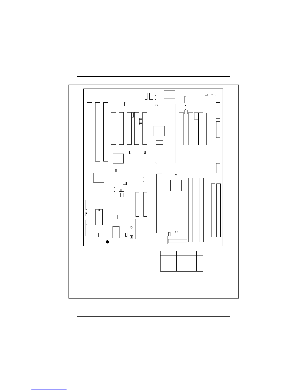
SUPER P6DLH
Figure 1-1. SUPER P6DLH Motherboard Picture
1-3
Page 14

SUPER P6DLH/P6DLF User’s Manual
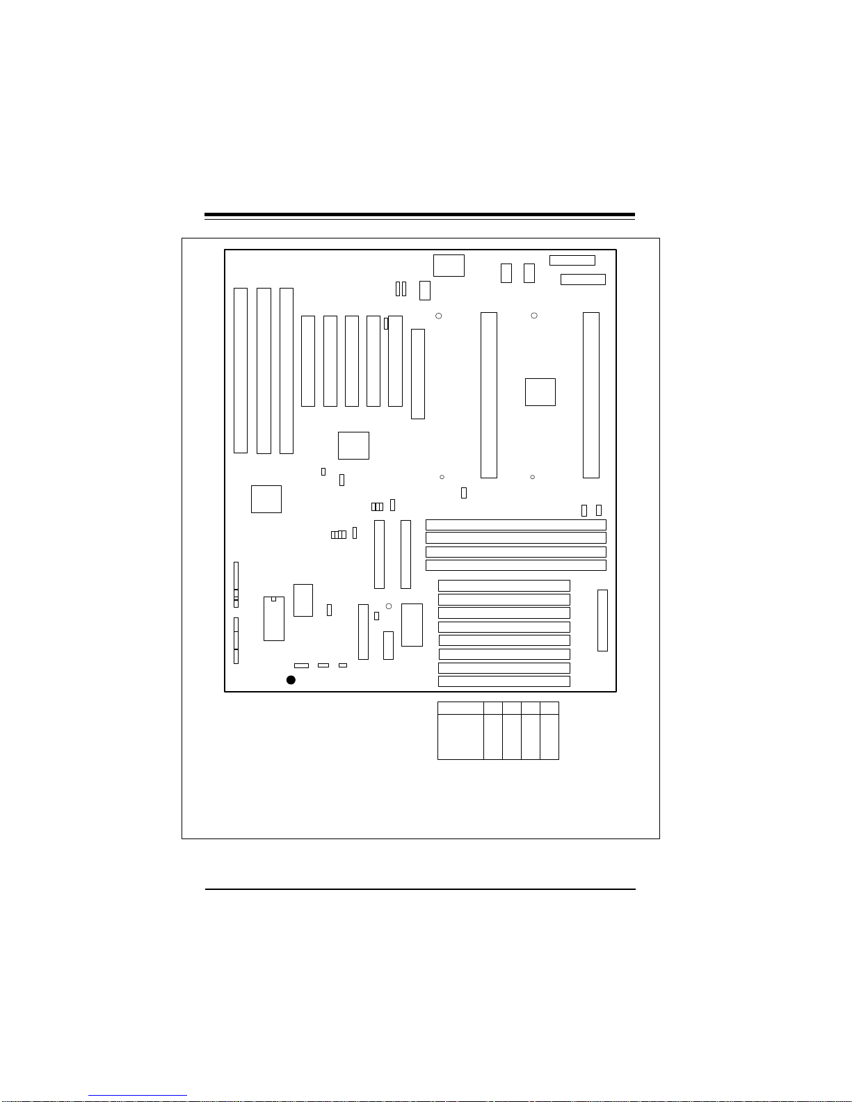
SUPER P6DLF
Figure 1-2. SUPER P6DLF Motherboard Picture
1-4
Page 15
J78
U45
U47
BIOS
CMOS
Clear
JBT1
1
J79
Ext
Battery
JBT2
1
J77
JF2
IR
CON
PW
ON
RESET
JF1
IDE
LED
KEY
LOCK
SPEAKER
SUPER
——–—— Manufacturer Settings ————
JL1: OFF (normal)
1-2 (reserved)
2-3 (intrusion detection)
JP17: 2-3
JP19: 1-2 APIC SMI (default)
2-3 PIIX4 SMI
JP26: 1-2 PIIX4 CTL
2-3 Save PD State (default)
JP917: ON
JP924: 1-2
JP925: 1-2
JBT1: 1-2 (default)
2-3 CMOS Clear
SW1: ON Enable BIOS AT/ATX Setting
SW2: OFF
——–———————–———–——–——–—
JP19
1
* J9 is PCI slave only
J9 J10
PCI 1
PCI 2
U14
SW2
JC2
JC3
JL1
1
JB1
JB2
JB3
JB4
1
1
WOL
JP85
JP26
1
BATTERY
-
JT3
BT2
+
®
P6DLH
J11
PCI 3
JC1
SW1
PWR
SEL
J12
1
J940
1
1
BZ1
JOH
JP88
J84
PCI 4
PCI 5
JP911
JP17
1
J15 J16
1
IDE 1
J22
FLOPPY
Chapter 1: Introduction
JP25 J18 J17
FAN1
1
1
USB
MOUSE
JP915
JP918
JP919
JP920
JP921
IDE 2
JT1
1
PS/2
J74 AT KB
IU20
i960 RD
i960 BIOS
J2
CPU 2
FAN2
1
VR3
CPU Core/
Bus Ratio
3.0
3.5
4.0
4.5
5.0
5.5
6.0
—————Bus Speed–————
MHz JC1 JC2 JC3
50 ON ON ON
60 ON OFF OFF
66 OFF OFF OFF
75 OFF ON OFF
——–—–——————————
JT2
J1
CPU 1
U9
PW2
ATX POWER
JB1
ON
OFF
ON
OFF
ON
OFF
ON
JP926
1
JT4
1
1
OFF
OFF
OFF
OFF
JB2
ON
ON
ON
1
JP925
JP924
JP917
ID4 ID3
JP21
1
COM2
J6J7J5
+5V EXTRA
Bank2
POWER
J918
Bank3
JP20
1
J19
1
PW1
1
PW5
J917
i960 MEM
COM1
PARALLEL
AT POWER
J943
1
J4
Bank0
Bank1
JB3
JB4
ON
ON
ON
ON
OFF
ON
OFF
ON
OFF
ON
OFF
ON
ON
OFF
Figure 1-3. P6DLH Motherboard Layout
1-5
Page 16
SUPER P6DLH/P6DLF User’s Manual
J78
J77
JF2
JF1
SUPER
——–—— Manufacturer Settings ————
JL1: OFF (normal)
JP17: 2-3
JP19: 1-2 APIC SMI (default)
JP26: 1-2 PIIX4 CTL
JBT1: 1-2 (default)
JP85: Wake-on-LAN
SW1: ON Enable BIOS AT/ATX Setting
——–———————–———–——–——–—
J79
J9 J10
PCI 1
PCI 2
SW1
U45
IR
CON
PW
ON
RESET
IDE
LED
KEY
LOCK
SPEAKER
BATTERY
-
U47
BT2
JP26
+
Ext
Battery
JBT2
1
®
P6DLF
1
CMOS
Clear
JBT1
1
BIOS
1-2 (reserved)
2-3 (intrusion detection)
2-3 PIIX4 SMI
2-3 Save PD State (default)
2-3 CMOS Clear
To clear the CMOS completely,
disconnect the power source.
JP85
WOL
JB1
OVER
HEAT
JOH
JB2
LED
J11
PCI 3
JB3
U14
1
1
JB4
JL1
J22
1
J18
1
USB2
J84
J12
1
JP19
PCI 4
PCI 5
JP17
1
JC3
JC1
JC2
J15
1
1
IDE 1
BZ1
JP86
PW5
FLOPPY
POWER +5V EXTRA
J17
J16
JP25
J74 AT KB
1
1
PS/2 MOUSE
USB1
J8
AGP
JT2
CPU 2 FAN
IDE 2
VR3
CPU Core/
Bus Ratio
3.0
3.5
4.0
4.5
5.0
5.5
6.0
—————Bus Speed–————
MHz JC1 JC2 JC3
50 ON ON ON
60 ON OFF OFF
66 OFF OFF OFF
75 OFF ON OFF
——–—–——————————
JP201 JP21
1
J2
CPU 2
Bank0
Bank1
Bank2
Bank3
JB1
ON
OFF
ON
OFF
ON
OFF
ON
JB2
OFF
OFF
ON
ON
OFF
OFF
ON
COM1
1
PW1
J19
1
PARALLEL
COM2
J1
U9
CPU 1
THERMAL
CONTROL
FAN
JT3 JT1
CPU 1 FAN
PW2
Bank0
Bank0
Bank1
Bank1
ATX POWER
Bank2
Bank2
Bank3
Bank3
JB3
JB4
ON
ON
ON
ON
OFF
ON
OFF
ON
OFF
ON
OFF
ON
ON
OFF
Figure 1-4. SUPER P6DLF Motherboard Layout
1-6
Page 17

Chapter 1: Introduction
SUPER P6DLH Features
The following list covers the general features of SUPER P6DLH:
CPU
• Dual Pentium II processor 233/266/300/333 MHz
I2O-Ready
• 66 MHz i960 RD IO processor
• up to 64 MB Local IOP memory
• 8 Mb Flash I/O BIOS
Memory
• 1 GB EDO or 512 MB SDRAM
• Error Checking and Correction and Parity Checking support
Chipset
• Intel 440LX
Expansion Slots
• 9 PCI slots
• 3 ISA slots
BIOS
• 2 Mbit AMI® Flash BIOS
• DMI 2.0, Plug and Play (PnP)
PC Health Monitoring (LM78)
• Seven on-board voltage monitors for CPU cores, CPU I/O,
+3.3V, ±5V, and ±12V
• Three-fan status monitors with firmware/software control on/off
• Chassis temperature monitor and control
• CPU fan auto-off in sleep mode
• System overheat control and alarm
• Chassis intrusion detection
• System resource alert
• Hardware BIOS virus protection
• Switching voltage regulators for the CPU core
• SUPERMICRO SUPER Doctor and Intel LANDesk Client
Manager (LDCM) support
1-7
Page 18

SUPER P6DLH/P6DLF User’s Manual
ACPI/PC 98 Features
• Microsoft OnNow
• Slow blinking LED for sleep-state indicator
• BIOS support for USB keyboard
• Real time clock wake-up alarm (ATX power only)
• Main switch override mechanism
• External modem ring-on if system is in SoftOff state
On-Board I/O
• 2 EIDE Bus Master interfaces support Ultra DMA/33 and Mode 4
• 1 floppy interface
• 2 Fast UART 16550 serial ports
• EPP (Enhanced Parallel Port) and ECP (Extended Capabilities
Port) parallel port
• PS/2 mouse port
• Infrared port
• 2 USB ports
Dimensions
• Full AT size (13.2" x 12.2")
1-8
Page 19

Chapter 1: Introduction
SUPER P6DLF Features
The following list covers the general features of SUPER P6DLF:
CPU
• Dual Pentium II processor 233/266/300/333 MHz
Memory
• 1 GB EDO or 512 MB SDRAM
• Error Checking and Correction and Parity Checking support
Chipset
• Intel 440LX
Expansion Slots
• 5 PCI slots
• 3 ISA slots
• 1 AGP slot
BIOS
• 2 Mbit AMI Flash BIOS
• DMI 2.0, Plug and Play (PnP)
PC Health Monitoring (LM78)
• Seven on-board voltage monitors for CPU cores, CPU I/O,
+3.3V, ±5V, and ±12V
• Three-fan status monitors with firmware/software control on/off
• Chassis temperature monitor and control
• CPU fan auto-off in sleep mode
• System overheat control and alarm
• Chassis intrusion detection
• System resource alert
• Hardware BIOS virus protection
• Switching voltage regulators for the CPU core
• SUPERMICRO SUPER Doctor and Intel LANDesk Client
Manager (LDCM) support
1-9
Page 20

SUPER P6DLH/P6DLF User’s Manual
ACPI/PC 98 Features
• Microsoft OnNow
• Slow blinking LED for sleep-state indicator
• BIOS support for USB keyboard
• Real time clock wake-up alarm (ATX power only)
• Main switch override mechanism
• External modem ring-on if system is in SoftOff state
On-Board I/O
• 2 EIDE Bus Master interfaces support Ultra DMA/33 and Mode 4
• 1 floppy interface
• 2 Fast UART 16550 serial ports
• EPP (Enhanced Parallel Port) and ECP (Extended Capabilities
Port) parallel port
• PS/2 mouse port
• Infrared port
• 2 USB ports
Dimensions
• Full AT size (13.2" x 12.2")
1-10
Page 21

Chapter 1: Introduction
1-2 PC Health Monitoring
This section describes the PC health monitoring features of SUPER
P6DLH/P6DLF. They have an on-board LM78 System Hardware
Monitor chip which supports PC health monitoring.
Seven On-Board Voltage Monitors for the CPU Cores,
CPU I/O, +3.3V, ±±5V, and ±±12V
The on-board voltage monitors will scan the seven monitored voltages every second. Once a voltage becomes unstable, it will report
a warning or an error message on the screen. Users can adjust
the threshold of the monitored voltage to determine the sensitivity of
the voltage monitor.
Three-Fan Status Monitors with Firmware/Software
Control On/Off
The PC health monitor can check the RPM status of the cooling
fans. The on-board 3-pin CPU fans are controlled by the ACPI BIOS
and the ACPI enabled operating system. The thermal fan is controlled by the overheat detection logic.
Chassis Temperature Control
The thermal control sensor will monitor the real-time chassis temperature. It will turn on the back-up fan whenever the chassis temperature goes over the user-defined threshold. The overheat circuitry runs independently from the CPU. It can still monitor the
overheat condition even if the CPU is in sleep mode. Once it detects that the chassis temperature is too high, it will automatically
turn on the back-up fan, trigger the overheat LED (JOH) and the
overheat buzzer (BZ1). The on-board chassis thermal circuitry can
monitor the overall system temperature and alert users when the
chassis temperature gets too high.
1-11
Page 22

SUPER P6DLH/P6DLF User’s Manual
CPU Fan Auto-Off in Sleep Mode
The CPU fan will turn on when the power is on. It can be turned off
when the CPU is in sleep mode. When the CPU is in sleep mode,
it means that it will not run at full power, thereby generating less
heat. For power saving purposes, the user can have the option to
shut down the CPU fan.
System Overheat Alarm and LED
This feature is available when used with SUPERMICRO's SUPER
Doctor Utility. The program will generate a beep sound via the
speaker when it detects system overheat condition. The overheat
condition can be configured by the user. The program can also give
an indication on the screen when the system overheats.
Chassis Intrusion Detection
The chassis intrusion circuitry can detect unauthorized intrusion to
the system. The chassis intrusion connector is located on JL1.
Attach a micro-switch to JL1. When the micro-switch is close, it
means that the chassis has been opened. The circuitry will then
alert the user with a warning message when the system is turned
on. The circuitry uses the on-board battery to power up. Even if the
whole system is powered off, the detection can still work properly.
System Resource Alert
This feature is available when used with Intel LANDesk Client Manager. The user can be notified of certain system events. For example, if the system is running low on virtual memory, the hard
drive space is not enough to save the data. LDCM will then send an
alert of the potential problems.
1-12
Page 23

Chapter 1: Introduction
Hardware BIOS Virus Protection
The system BIOS is protected by hardware so that no virus can
infect the BIOS area. The user can only change the BIOS content
through the flash utility provided by SUPERMICRO. This feature can
prevent viruses from infecting the BIOS area and from losing your
valuable data.
Switching Voltage Regulator for the CPU Core
The switching voltage regulator for the CPU core can support up to
20A current, with auto-sensing voltage ID ranging from 1.3V to 3.5V.
This will allow the regulator to run cooler and to make the system
more stable.
Intel LANDesk Client Manager (LDCM) Support
As the computer industry grows, PC systems have become more
complex and harder to manage. Historically, only experts have
been able to fully understand and control these complex systems.
Today's users want manageable systems that interact automatically
with the user. Client Manager enables both administrators and clients to:
• Review system inventory
• View DMI-compliant component information
• Back-up and restore system configuration files
• Troubleshoot
• Receive notification for system events
• Transfer files to and from client workstations
• Remotely reboot client workstations
1-13
Page 24

SUPER P6DLH/P6DLF User’s Manual
1-3 ACPI/PC 98 Features
ACPI stands for Advanced Configuration and Power Interface. The
ACPI specification defines a flexible and abstract hardware interface that provides a standard way to integrate power management
features throughout a PC system, including hardware, operating
system and application software. This enables the system to automatically turn on and off peripherals such as CD-ROMs, network
cards, hard disk drives, and printers. This also includes consumer
devices connected to the PC such as VCRs, TVs, phones, and stereos.
In addition to enabling operating system-directed power management, ACPI provides a generic system event mechanism for Plug
and Play and an operating system-independent interface for configuration control. ACPI leverages the Plug and Play BIOS data
structures while providing a processor architecture-independent
implementation that is compatible with both Windows 95 and Windows NT.
Microsoft OnNow
The OnNow design initiative is a comprehensive, system-wide approach to system and device power control. OnNow is a term for a
PC that is always on but appears off and responds immediately to
user or other requests.
Slow Blinking LED for Sleep-state Indicator
When the CPU goes into a sleep state, the power LED will start
blinking to indicate that the CPU is in sleep mode. When the user
presses any key, the CPU will wake-up and the LED will automatically stop blinking and remain on.
1-14
Page 25

Chapter 1: Introduction
BIOS Support for USB Keyboard
If the USB keyboard is the only keyboard in the system, the USB
keyboard will work like a normal keyboard during system boot-up.
Real Time Clock Wake-up Alarm (ATX power only)
The PC is perceived to be off when not in use, but is still capable of
responding to wake-up events due to a scheduled date and time of
the month. The user can set up a timer to wake-up or shutdown the
system at some predetermined time.
Main Switch Override Mechanism
When an ATX power supply is used, the power button can function
as a system suspend button. When the user press on the power
button, the system will enter a SoftOff state. The monitor will be
suspended, and the hard drive will spin down. Pressing the power
button again will cause the whole system to wake-up. During the
SoftOff state, the ATX power supply provides power to keep the required circuitry on the system alive. In case the system malfunctions and you want to turn off the power, just press down on the
power button for approximately 4 seconds. The power will turn off
and no power is provided to the motherboard.
External Modem Ring-on if System is in SoftOff State
Wake-up events can be triggered by a device such as the external
modem ringing when the system is in SoftOff state.
1-4 Chipset Overview
The 440LX chipset is developed by Intel as the ultimate Pentium II
processor platform targeted for emerging 3D graphics and multimedia applications. Along with System-to-PCI bridge integrated
with optimized DRAM controller and data path, the chipset intro-
1-15
Page 26

SUPER P6DLH/P6DLF User’s Manual
duces the Accelerated Graphics Port (AGP) interface. AGP is a high
performance, component level interconnect targeted at 3D applications and is based on a set of performance enhancements to PCI.
The I/O subsystem portion of the 440LX platform is based on the
PIIX4, a highly integrated version of Intel's PCI-to-ISA bridge family.
The 440LX PCI/AGP Controller (PAC) system bus interface supports
up to two Pentium II processors. It provides an optimized 72-bit
DRAM interface (64-bit data plus ECC). This interface supports
3.3V DRAM technologies. The PAC provides the interface to a PCI
bus operating at 33 MHz. This interface implementation is compliant with the PCI Rev 2.1 Specification. The AGP interface is based
on the AGP Specification Rev 1.0. It can support up to 133 MHz
(532 MB/s) data transfer rates.
1-5 Wake-On-LAN (WOL)
Wake on LAN is defined as the ability of a management application
to remotely power up a computer which is powered off. Remote PC
setup, updates, and asset tracking can occur after hours and on
weekends so daily LAN traffic is kept to a minimum and users are
not interrupted.
The motherboard has a 3-pin header (WOL) used to connect to the
3-pin header on the Network Interface Card (NIC) which has WOL
capability.
1-6 Power Supply
As with all computer products, a stable power source is necessary
for proper and reliable operation. It is even more important for high
CPU clock rates like 300, 266, 233 MHz Pentium II processors.
SUPER P6DLH/P6DLF accommodates AT and ATX power supplies.
Although most power supplies generally meet the specifications required by the CPU, some power supplies are not adequate. To
1-16
Page 27

Chapter 1: Introduction
obtain the highest system reliability, be certain that your AT power
supply provides +5 VDC with a voltage range between +4.95 VDC
(minimum) and +5.25 VDC (maximum).
It is highly recommended that you use a high quality power supply.
Additionally, in areas where noisy power transmission is present,
you may choose to install a line filter to separate noise from the
computer. You can also install a power surge protector to help
avoid problems caused by power surges.
1-7 National Semiconductor Super I/O Controller
The National Semiconductor 87307 Super I/O Controller incorporates an IDE control logic, two full function serial ports, an IEEE
1284 parallel port, industry standard floppy disk controller with 16
byte FIFO, Real Time Clock and an 8042 compatible keyboard controller all in one chip.
The IDE interfaces provide up to Mode 4 support. The two serial
ports are software compatible with the Fast UART 16550. The parallel port is EPP (Enhanced Parallel Port) and ECP (Extended Capabilities Port) compatible, including level 2 support. It includes a
protection circuit against damage caused when the printer is powered up. EPP mode provides for greater throughput than Compatible or Extended modes by supporting faster transfer rates and a
mechanism that allows the host to address peripheral device registers directly. Faster transfers are achieved by automatically generating the address and data strobes. EPP is compatible with both
Compatible and Extended mode parallel-port devices.
1-17
Page 28

SUPER P6DLH/P6DLF User’s Manual
1-8 Warranty, Technical Support, and Service
The manufacturer will repair or exchange any unit or parts free of
charge due to manufacturing defects for one year (12 months) from
the original invoice date of purchase.
Parts
Defective parts will be exchanged or repaired within one year (12
months) from the manufacturer’s original invoice purchase date.
BIOS
The manufacturer will exchange the BIOS (shipping and handling
excluded) due to existing incompatibility issues within one year
from the manufacturer’s original invoice purchase date.
Labor
Mail-in or carry-in service is available for one year (12 months) from
the manufacturer’s original invoice purchase date.
Returns
If you must return products for any reason, refer to Chapter 3 in this
manual, “Returning Merchandise for Service.”
1-18
Page 29

Chapter 2: Installation
Chapter 2
Installation
2-1 Pentium II Processor Installation
1. Check the Intel boxed processor kit for the following items: the
processor with the fan heatsink attached, two black plastic pegs,
two black plastic supports, and one power cable.
2. Install the retention mechanism attach mount under the
motherboard. Do this before mounting the motherboard into the
chassis. Do not screw too tight. Mount the two black plastic pegs
onto the motherboard (Figure 2.1). These pegs will be used to
attach the fan heatsink supports. Notice that one hole and the base
of one peg are larger than the other hole and peg base. Push each
peg into its hole firmly until you hear it "click" into place.
Figure 2-1. Mounting the Pegs
Retention
Mechanism
Large peg and hole
2-1
Page 30

SUPER P6DLH/P6DLF User’s Manual
3. Slide a black plastic support onto each end of the fan heatsink,
making sure that the hole and clip are on the outside edge of the
support. If the supports are reversed, the holes will not line up with
the pegs on the motherboard. Slide each support toward the center
of the processor until the support is seated in the outside groove in
the fan housing.
Figure 2-2. Support for Fan Heatsink
Top of processor
Groove in fan housing
Hole and clip on outside edge
2-2
Page 31

Chapter 2: Installation
4. Slid the clip (A) on each support toward the processor, exposing
the hole that will fit over the peg on the motherboard. Push the
latches (B) on the processor toward the center of the processor
until they click into place.
5. Hold the processor so that the fan shroud is facing toward the
pegs on the motherboard. Slide the processor (C) into the retention mechanism and slide the supports onto the pegs. Ensure that
the pegs on the motherboard slide into the holes in the heatsink
support and that the alignment notch in the SEC cartridge fits over
the plug in Slot 1. Push the processor down firmly, with even pressure on both sides of the top, until it is seated.
Figure 2-3. Retention Mechanism
B
C
A
Do not screw too tight!
2-3
Page 32

SUPER P6DLH/P6DLF User’s Manual
6. Slide the clips on the supports (A) forward until they click into
place to hold the pegs securely. Apply slight pressure on the peg
and push the peg toward the clip while pushing the clip forward.
Push the latches on the processor (B) outward until they click into
place in the retention mechanism. The latches must be secured for
proper electrical connection of the processor.
7. Attach the small end of the power cable (C) to the three-pin con-
nector on the processor, then attach the large end to the three-pin
connector on the motherboard.
Figure 2-4. Attaching the Power Cable
B
C
A
2-4
Page 33

Chapter 2: Installation
OEM Pentium II and Heat Sink Support
The heat sink support shown on Figure 2-5 consists of a top bar, a
base bar, four posts on the top bar and two posts on the base bar.
The two posts on the base snaps into the motherboard. Install the
two pins into the base bar. Insert the Pentium II with the heat sink
on it into Slot 1. Install the top support bar. The four top posts
should be close to Slot 1. The bottommost row of fins in the heat
sink should fit between the top support bar and the bottom support
bar as shown in Figure 2-6.
Figure 2-5. Heat Sink Support
Figure 2-6. Pentium II Heat Sink
2-5
Heat Sink
Page 34

SUPER P6DLH/P6DLF User’s Manual
Removing the Pentium II Processor
To remove the Pentium II processor from the motherboard, follow
these steps (the reverse of the installation process).
1. Disconnect the fan power cable from the motherboard. It is rec-
ommended to leave the cable connected to the processor.
2. Slide the clips on the supports backward to release the pegs in
the motherboard. Push the latches on the processor toward the
center of the processor until they click into place.
3. Lift one end of the processor until it is freed from Slot 1. Lift the
other end of the processor until it is freed from Slot 1. Lift the entire
processor (with the fan heatsink supports attached) until it is free
from the retention mechanism.
4. Remove the heatsink support pegs from the motherboard and
discard them. With one hand, squeeze together the two halves of
the peg on the bottom side of the motherboard. With the other
hand, pull the peg out of the hole in the motherboard. Do not reuse
the pegs.
When handling the Pentium II processor, avoid
placing direct pressure on the label area of the fan.
When removing the Pentium II processor, avoid pressing
down on the motherboard or components. Instead,
press down on the plastic connectors.
2-6
Page 35

Chapter 2: Installation
2-2 Static-Sensitive Devices
Static-sensitive electric discharge can damage electronic components. To prevent damage to your system board, it is important
to handle it very carefully. The following measures are generally
sufficient to protect your equipment from static discharge.
Precautions
• Use a grounded wrist strap designed for static discharge.
• Touch a grounded metal object before you remove the board
from the anti-static bag.
• Handle the board by its edges only; do not touch its components, peripheral chips, memory modules, or gold contacts.
• When handling chips or modules, avoid touching their pins.
• Put the system board and peripherals back into their anti-static
bags when not in use.
• Be sure your computer system’s chassis allows excellent
conductive contacts between its power supply, case, mounting
fasteners, and the system board for grounding purposes.
Unpacking
The system board is shipped in anti-static packaging to avoid static
damage. When unpacking the board, be sure the person handling
the board is static-protected.
2-3 Changing the CPU Speed
To change the CPU speed for a Pentium II processor, change the
jumpers shown on Table 2-1. Refer to Table 2-2 for the external
bus speed jumper settings. The default bus speed is 66 MHz. The
following example will show you which CPU Core/Bus Ratio to use.
The general rule is to divide the CPU speed by the bus speed (66
MHz). If you have a 266 MHz CPU, dividing it by 66 will give you a
2-7
Page 36

SUPER P6DLH/P6DLF User’s Manual
CPU Core/Bus Ratio of 4. After determining the CPU Core/Bus
Ratio, refer to Table 2-1 for the jumper settings of JB1, JB2, JB3
and JB4.
CPU Core/Bus Ratio = CPU Speed
Bus Frequency
CPU Core/Bus Ratio = 266 MHz = 4.0
66 MHz
Table 2-1. Pentium II Speed Selection
CPU Core/ JB1 JB2 JB3 JB4
Bus Ratio
3.0 ON OFF ON ON
3.5 OFF OFF ON ON
4.0 ON ON OFF ON
4.5 OFF ON OFF ON
5.0 ON OFF OFF ON
5.5 OFF OFF OFF ON
6.0 ON ON ON OFF
Table 2-2. External Bus Speed Selection
MHz JC1 JC2 JC3
50 ON ON ON
60 ON OFF OFF
66 OFF OFF OFF
75 OFF ON OFF
2-4 Mounting the Motherboard in the Chassis
SUPER P6DLH/P6DLF has standard mounting holes to fit different
types of chassis. Chassis may come with a variety of mounting
fasteners, made of metal or plastic. Although a chassis may have
both metal and plastic fasteners, metal fasteners are the most
2-8
Page 37

Chapter 2: Installation
highly recommended because they ground the system board to the
chassis. Therefore, use as many metal fasteners as possible for
better grounding.
2-5 Connecting Cables
Power Supply Connector
After you have securely mounted the motherboard to the chassis,
you are ready to connect the cables. Attach power supply cables to
PW1 for a 5V power supply or PW2 for ATX power supply. Do not
force the cables, but make sure they are fully seated. The two black
wires on each power cable for PW1 sit next to each other when
correctly installed. See Table 2-3 for pin definitions of an ATX power
supply. See Table 2-4 for pin definitions of a 5V power supply. See
Table 2-5 for pin definitions of the extra 5V power supply.
Table 2-3. ATX Power Supply Connector Pin Definitions
Connector Pin Pin
Number Number Function Number Function
PW2 1 3.3V 11 3.3V
2 3.3V 12 -12V
3 COM 13 COM
4 5V 14 PS-ON
5 COM 15 COM
6 5V 16 COM
7 COM 17 COM
8 PW-OK 18 -5V
9 5VSB 19 5V
10 12V 20 5V
2-9
Page 38

SUPER P6DLH/P6DLF User’s Manual
Table 2-4. 5V AT Power Supply Connector Pin Definitions
Connector Pin
Number Number Function
PW1 1 Power Good (Power on reset, TTL signal)
2 +5 VCC
3 +12 VCC
4 -12 VCC
5 Ground (Black wire to be connected)
6 Ground (Black wire to be connected)
7 Ground (Black wire to be connected)
8 Ground (Black wire to be connected)
9 -5 VCC
10 +5 VCC
11 +5 VCC
12 +5 VCC
Table 2-5. Extra 5V Power Supply Connector Pin Definitions
Connector Pin
Number Number Function
PW5 1 +5 VCC
2 +5 VCC
3 +5 VCC
4 Ground (Black wire to be connected)
5 Ground (Black wire to be connected)
6 Ground (Black wire to be connected)
2-10
Page 39

Chapter 2: Installation
PW_ON Connector
The PW_ON connector is located on pins 9 and 10 of JF2. Momentary contacting both pins will power on/off the system. To turn off
the power, hold down the power button for at least 4 seconds. In
order to have the "4 seconds" feature, you need to enable the Power
Management/APM in the BIOS and set the Power Button Function to
Suspend. See Table 2-6 for pin definitions.
Table 2-6. PW_ON Connector Pin Definitions
Pin
Number Definition
9 PW_ON
10 Ground
Infrared Connector
The infrared connector is located on pins 1-8 of JF2. See Table 27 for pin definitions.
Table 2-7. Infrared Pin Definitions
Pin
Number Definition
1 +5V
2 Key
3 IRRX
4 Ground
5 IRTX
6 IRSEL0
7 IRSEL1
8 IRSEL2
2-11
Page 40

SUPER P6DLH/P6DLF User’s Manual
Reset Connector
The reset connector is located on pins 12 and 13 of JF2. This
connector attaches to the hardware Reset switch on the computer
case. See Table 2-8 for pin definitions.
Table 2-8. Reset Pin Definitions
Pin
Number Definition
12 Reset
13 Ground
Keylock/Power LED Connector
The keylock/power LED connector is located on pins 5 to 9 of JF1.
See Table 2-9 for pin definitions. Pins 5 and 7 are for the power
LED. Pins 8 and 9 are for the keylock.
Table 2-9. Keylock/Power LED Pin Definitions
Pin
Number Function Definition
5 + Red wire, LED power
6 Key No connection
7 GND Black wire
8 Keyboard inhibit
9 GND Black wire
2-12
Page 41

Chapter 2: Installation
Hard Drive LED
The hard drive LED is located on pins 1 to 4 of JF1. Attach the hard
drive LED cable onto pins 1 and 2. See Table 2-10 for pin definitions.
Table 2-10. Hard Drive LED Pin Definitions
Pin
Number Definition
1 +5V
2 Key
3 HD Active
4 +5V
Speaker Connector
The speaker connector is located on pins 10 to 13 of JF1. See
Table 2-11 for pin definitions.
Table 2-11. Speaker Connector Pin Definitions
Pin
Number Function Definition
10 + Red wire, speaker data
11 Key No connection
12 VCC Speaker data
13 GND Black wire
2-13
Page 42

SUPER P6DLH/P6DLF User’s Manual
AT Keyboard Connector
The keyboard connector J74 has five pins. See Table 2-12 for pin
definitions.
Table 2-12. Keyboard Connector Pin Definitions
Pin
Number Function
1 Keyboard clock
2 Keyboard data
3 Spare
4 Ground
5 +5 VDC
Universal Serial Bus
The Universal Serial Bus is located on J17 and J18. See Table 213 for pin definitions.
Table 2-13. USB Pin Definitions
Pin J17 Pin J18
Number Function Number Function
1 +5V 1 +5V
2 P0- 2 P0 3 P0+ 3 P0+
4 GND 4 GND
5 N/A 5 Key
2-14
Page 43

Chapter 2: Installation
PS/2 Mouse Port
The PS/2 Mouse port is located on JP25. See Table 2-14 for pin
definitions.
Table 2-14. PS/2 Mouse Pin Definitions
Pin Pin
Number Function Number Function
1 NC 2 NC
3 NC 4 CLK
5 NC 6 VCC
7 Data 8 NC
9 GND 10 NC (key)
Serial Ports
Serial port COM1 is located on JP20 and serial port COM2 is located on JP21. See Table 2-15 for pin definitions.
Table 2-15. Serial Ports Pin Definitions
Pin Pin
Number Function Number Function
1 DCD 6 CTS
2 DSR 7 DTR
3 Serial In 8 RI
4 RTS 9 GND
5 Serial Out 10 NC
2-15
Page 44

SUPER P6DLH/P6DLF User’s Manual
Power On/Off State
Refer to Table 2-16 on how to set JP26. Save Power Down (PD)
State is the default and is used when you want the system to be in
power off state the first time you apply power to the system or when
the system comes back from AC power failure. PIIX4 control is
used if you want the system to be in power on state the first time
you apply power to the system or when the system comes back
from AC power failure.
Table 2-16. Power On/Off State Pin Definitions
Connector Jumper
Number Position Function
JP26 1-2 PIIX4 Ctrl
2-3 Save PD State
SMI
Refer to Table 2-17 for instructions on how to use JP19. This
jumper should normally be set to 1-2 APIC SMI.
Table 2-17. SMI Pin Definitions
Connector Jumper
Number Position Function
JP19 1-2 APIC SMI
2-3 PIIX4 SMI
2-16
Page 45

Chapter 2: Installation
CMOS Clear
Refer to Table 2-18 for instructions on how to clear the CMOS. For
ATX power supply, you need to completely shut down the system,
then use JBT1 to clear the CMOS. Do not use the PW_ON connec-
tor to clear the CMOS.
Table 2-18. CMOS Clear Pin Definitions
Connector Jumper
Number Position Function
JBT1 1-2 Normal
2-3 CMOS Clear
External Battery
Refer to Table 2-19 to connect an external battery to JBT2.
Table 2-19. External Battery Pin Definitions
Pin Number Function
1 +3 V
2 NC
3 NC
4 Ground
Overheat LED
Refer to Table 2-20 to connect an LED to JOH for overheat warning.
Table 2-20. Overheat LED Pin Definitions
Pin Number Function
1 +12 V
2 Signal
2-17
Page 46

SUPER P6DLH/P6DLF User’s Manual
Buzzer Overheat Notification
Refer to Table 2-21 for instructions on how to use JP86 (P6DLF) or
JP88 (P6DLH) to enable or disable the buzzer BZ1.
Table 2-21. Buzzer Selection Pin Definitions
Jumper
Position Function
ON Enable Buzzer
OFF Disable Buzzer
Chassis Intrusion Connector
Refer to Table 2-22 for the chassis intrusion located on JL1.
Table 2-22. Chassis Intrusion Pin Definitions
Pin
Number Function
1 Standby +5V
2 Intrusion Input
3 Ground
Power Supply Selection
Use SW1 to select the type of power supply used in the system.
Refer to Table 2-23 for pin definitions.
Table 2-23. SW1 Pin Definitions
Jumper
Position Function
ON Enable BIOS AT/ATX Setting
OFF ATX Power Supply
2-18
Page 47

Chapter 2: Installation
Wake-on-LAN
The Wake-on-LAN connector is located on JP85. Refer to Table 224 for pin definitions.
Table 2-24. Wake-on-LAN Pin Definitions
Pin
Number Function
1 +5V Standby
2 Ground
3 Wake up
Fan Connectors*
The CPU fans are located on JT1 and JT2. The overheat fan with
tachometer sensor input is located on JT3. The overheat fan without tachometer sensor input is located on JT4 (P6DLH only). Refer
to Table 2-25 for pin definitions.
Table 2-25. Fan Pin Definitions
Pin
Number Function
1 Ground
2 +12 V
3 Tachometer
* Caution: These connectors are DC direct.
2-19
Page 48

SUPER P6DLH/P6DLF User’s Manual
Optional Keyboard Connector (P6DLH)
SUPER P6DLH has an extra keyboard header, JP926, which can be
used for certain chassis that provides for a front keyboard connection. Refer to Table 2-26 for the pin definitions.
Table 2-26. Keyboard Connector Pin Definitions
Pin
Number Function
1 Keyboard clock
2 Keyboard data
3 Spare
4 Ground
5 +5 VDC
i960 Serial Port (P6DLH)
The i960 serial port is located on J943. Refer to Table 2-27 for pin
definitions.
Table 2-27. i960 Serial Port Pin Definitions
Pin Pin
Number Function Number Function
1 CD 6 DSR
2 TXD 7 CTS
3 RXD 8 RTS
4 DTR 9 X
5 GND 10 NC
2-20
Page 49

Chapter 2: Installation
i960 Fail LED Indicator (P6DLH)
ID4 is used to determine whether Mode 3 of the i960 RD IO processor is functioning properly. Refer to Table 2-28 for the LED indications.
Table 2-28. i960 Fail LED Definitions
LED Status Definition
OFF i960 Mode 3 OK
ON i960 Mode 3 failed
i960 is in Mode 0
i960 Initialization Modes (P6DLH)
Refer to Table 2-29 for instructions on setting the mode.
Table 2-29. i960 Mode Settings
Jumper Mode 3 Mode 0
(default)
JP915 OFF OFF
JP918 OFF ON
JP919 OFF ON
JP920 OFF OFF
JP921 ON ON
2-21
Page 50

SUPER P6DLH/P6DLF User’s Manual
i960 Jumper Settings (P6DLH)
Refer to Table 2-30 for more jumper settings related to the i960
IOP.
Table 2-30. i960 Jumper Settings
Jumper Default Definition
JP911 OFF Enables the internal
secondary arbiter
JP917 ON Enable I/O IRQ
OFF Ext. debugging mode
JP924 1-2 12V enable
JP925 1-2 Flash enable
I2C Connector (P6DLH)
The I2C connector located on J940 is for development purposes
only. Refer to Table 2-31 for pin definitions.
Table 2-31. I2C Pin Definitions
Pin
Number Function
1 SDA
2 Ground
3 SCL
4 VCC
2-22
Page 51

Chapter 2: Installation
2-6 Installing/Removing the SIMM/DIMM Modules
SUPER P6DLH can accommodate a maximum of 1 GB EDO DIMMs
or 512 MB SDRAM DIMMs. It has 4 168-pin unbuffered DIMM slots.
It is not recommended to mix EDO DIMM modules with SDRAM
DIMM modules.
SUPER P6DLF can accommodate a maximum of 1 GB EDO SIMMs
or 1 GB EDO DIMMs or 512 MB SDRAM DIMMs. It has 8 72-pin
SIMM slots and 4 168-pin 3.3V unbuffered DIMM slots. You can only
use one type of memory at a time. That means you cannot mix
SIMM modules with DIMM modules and vice versa. It is not recommended to mix EDO DIMM modules with SDRAM DIMM modules.
The 5V EDO SIMM slots are provided so that users can still use
their memory when they upgrade their old system to a Pentium IIbased motherboard. However, it is not recommended to use 5V
EDO SIMMs together with an AGP card.
There are three types of EDO and SDRAM DIMM modules: x4, x8
and x16. If you are using the x4 type, you can populate the DIMM
slots with either 4 single-sided memories or 2 double-sided memories. For memory configurations of 512 MB EDO DIMMs or higher, it
is recommended to use x8 or x16 type of memory.
There are no jumpers needed to configure the on-board memory.
Memory timing requires 70ns or faster for EDO memory. Refer to
Figure 2-7 and the instructions below for installing or removing
DIMM modules.
CAUTION
Exercise extreme care when installing or removing the
SIMM/DIMM modules to prevent any possible damages.
2-23
Page 52

SUPER P6DLH/P6DLF User’s Manual
To Remove:
Use your thumb to gently push the edge of
the socket and release the module. Do this
on both sides for each module.
To Install:
Insert
vertically,
press down
until it snap
into place.
Pay attention
to the two
notches.
DIMM
Figure 2-7. Installing/Removing a DIMM Memory Module
SIMM/DIMM Module Installation
1. Insert SIMM/DIMM modules in Bank 0 through Bank 3 as
required for the desired system memory.
2. Insert each DIMM module vertically into its socket. Pay
attention to the two notches to prevent inserting the DIMM at a
wrong position. The component side of the DIMM module
must face the CPU socket. The latter statement is applicable
for DIMMs with components on one side only. Gently press
the DIMM module until it snaps upright into place in the
socket.
3. Insert each SIMM module into its socket at an angle. Gently
press the SIMM module until it snaps upright into place in the
socket.
2-24
Page 53

Chapter 2: Installation
Removing DIMM Modules
1. Remove DIMM modules in any order.
2. Gently push the edge of the sockets to the side to release the
module. Remove one side of the DIMM module first, and then
the other side, to prevent breaking the socket.
Removing SIMM Modules
1. Remove SIMM modules from Bank 0 through Bank 3.
2. Gently push the edge of the sockets to the side to release the
module. Remove one side of the SIMM module first, and then
the other side, to prevent breaking the socket.
2-25
Page 54

SUPER P6DLH/P6DLF User’s Manual
2-7 Connecting Parallel, Floppy and Hard Disk
Drives
Use the following information to connect the floppy and hard disk
drive cables.
• The floppy disk drive cable has seven twisted wires.
• A red mark on a wire typically designates the location of pin 1.
• A single floppy disk drive ribbon cable has 34 wires and two
connectors to provide for two floppy disk drives. The connector
with twisted wires always connects to drive A, and the connector
that does not have the twisted wires always connects to drive B.
• An IDE hard disk drive requires a data ribbon cable with 40 wires,
and a SCSI hard disk drive requires a SCSI ribbon cable with 50
wires. A wide SCSI hard disk drive requires a SCSI ribbon cable
with 68 wires.
• A single IDE hard disk drive cable has two connectors to provide
for two drives. To select an IDE disk drive as C, you would normally set the drive select jumper on the drive to DS1. To select
an IDE disk drive as D, you would normally set the drive select
jumper on the drive to DS2. Consult the documentation that
came with your disk drive for details on actual jumper locations
and settings.
• A single SCSI ribbon cable typically has three connectors to provide for two hard disk drives and the SCSI adapter. (Note: most
SCSI hard drives are single-ended SCSI devices.) The SCSI ID
is determined by jumpers or a switch on the SCSI device. The
last internal (and external) SCSI device cabled to the SCSI
adapter must be terminated.
• Some drives require a special controller card. Read your disk
drive manual for details.
2-26
Page 55

Chapter 2: Installation
Parallel Port Connector
The parallel port is located on J19. See Table 2-32 for pin definitions.
Table 2-32. Parallel Port Pin Definitions
Pin Pin
Number Function Number Function
1 Strobe- 2 Auto Feed 3 Data Bit 0 4 Error 5 Data Bit 1 6 Init 7 Data Bit 2 8 SLCT IN 9 Data Bit 3 10 GND
11 Data Bit 4 12 GND
13 Data Bit 5 14 GND
15 Data Bit 6 16 GND
17 Data Bit 7 18 GND
19 ACJ- 20 GND
21 BUSY 22 GND
23 PE 24 GND
25 SLCT 26 NC
2-27
Page 56

SUPER P6DLH/P6DLF User’s Manual
Floppy Connector
The floppy connector is located on J22. See Table 2-33 for pin
definitions.
Table 2-33. Floppy Connector Pin Definitions
Pin Pin
Number Function Number Function
1 GND 2 FDHDIN
3 GND 4 Reserved
5 Key 6 FDEDIN
7 GND 8 Index9 GND 10 Motor Enable
11 GND 12 Drive Select B13 GND 14 Drive Select A15 GND 16 Motor Enable
17 GND 18 DIR19 GND 20 STEP21 GND 22 Write Data23 GND 24 Write Gate25 GND 26 Track 0027 GND 28 Write Protect29 GND 30 Read Data31 GND 32 Side 1 Select33 GND 34 Diskette
2-28
Page 57

Chapter 2: Installation
IDE Interfaces
There are no jumpers to configure the on-board IDE interfaces J15
and J16. Refer to Table 2-34 for the pin definitions.
Table 2-34. IDE Connector Pin Definitions
Pin Pin
Number Function Number Function
1 Reset IDE 2 GND
3 Host Data 7 4 Host Data 8
5 Host Data 6 6 Host Data 9
7 Host Data 5 8 Host Data 10
9 Host Data 4 10 Host Data 11
11 Host Data 3 12 Host Data 12
13 Host Data 2 14 Host Data 13
15 Host Data 1 16 Host Data 14
17 Host Data 0 18 Host Data 15
19 GND 20 Key
21 DRQ3 22 GND
23 I/O Write- 24 GND
25 I/O Read- 26 GND
27 IOCHRDY 28 BALE
29 DACK3- 30 GND
31 IRQ14 32 IOCS1633 Addr 1 34 GND
35 Addr 0 36 Addr 2
37 Chip Select 0 38 Chip Select 139 Activity 40 GND
2-29
Page 58

SUPER P6DLH/P6DLF User’s Manual
AGP Port (P6DLF)
There are no jumpers to configure the AGP port J8. Refer to Table
2-35 for the pin definitions.
Table 2-35. AGP Port Pin Definitions
Pin# B A
1 Spare 12V
2 5.0V Spare
3 5.0V Reserved *
4 USB+ USB5 GND GND
6 INTB# INTA#
7 CLK RST#
8 REQ# GNT#
9 VCC3.3 VCC3.3
10 ST0 ST1
11 ST2 Reserved
12 RBF# PIPE#
13 GND GND
14 Spare Spare
15 SBA0 SBA1
16 VCC3.3 VCC3.3
17 SBA2 SBA3
18 SB_STB Reserved
19 GND GND
20 SBA4 SBA5
21 SBA6 SBA7
22 KEY KEY
23 KEY KEY
24 KEY KEY
25 KEY KEY
26 AD31 AD30
27 AD29 AD28
28 VCC3.3 VCC3.3
29 AD27 AD26
2-30
Page 59

Chapter 2: Installation
30 AD25 AD24
31 GND GND
32 AD_STB1 Reserved
33 AD23 C/BE3#
34 Vddq3.3 Vddq3.3
35 AD21 AD22
36 AD19 AD20
37 GND GND
38 AD17 AD18
39 C/BE2# AD16
40 Vddq3.3 Vddq3.3
41 IRDY# FRAME#
42
43 GND GND
44
45 VCC3.3 VCC3.3
46 DEVSEL# TRDY#
47 Vddq3.3 STOP#
48 PERR# Spare
49 GND GND
50 SERR# PAR
51 C/BE1# AD15
52 Vddq3.3 Vddq3.3
53 AD14 AD13
54 AD12 AD11
55 GND GND
56 AD10 AD9
57 AD8 C/BE0#
58 Vddq3.3 Vddq3.3
59 AD_STB0 Reserved
60 AD7 AD6
61 GND GND
62 AD5 AD4
63 AD3 AD2
64 Vddq3.3 Vddq3.3
65 AD1 AD0
66 SMB0 SMB1
2-31
Page 60

SUPER P6DLH/P6DLF User’s Manual
2-32
Page 61

Chapter 3: Troubleshooting
Chapter 3
Troubleshooting
3-1 Troubleshooting Procedures
Use the following procedures to troubleshoot your system. If you
have followed all of the procedures below and still need assistance,
refer to the ‘Technical Support Procedures’ and/or ‘Returning
Merchandise for Service’ section(s) in this chapter.
No Video
Use the following steps for troubleshooting your system configuration.
1. If you have no video, remove all the add-on cards and cables.
2. Check for shorted connections, especially under the
motherboard.
3. Check the jumpers settings, clock speed, and voltage settings.
4. Use the speaker to determine if any beep codes exist. Refer to
Appendix C of the AMI BIOS Reference Manual for details about
beep codes.
3-1
Page 62

SUPER P6DLH/P6DLF User’s Manual
Install only the CPU, memory, and speaker
Power
On
N
Power
LED on?
Speaker
Beeps?
Power
Supply OK?
N
Y
Replace
Power
Supply
Check memory,
BIOS
and CPU
Y
8 beeps
Y
Motherboard
N
Good
Speaker
Beeps?
Replace
Motherboard
Y
N
Figure 3-1. Troubleshooting Flowchart
3-2
Page 63

Chapter 3: Troubleshooting
NOTE
If you are a system integrator, VAR or OEM, a POST
diagnostics card is recommended for port 80h codes.
Refer to Appendix D.
Memory Error
If you encounter memory error, follow the procedures below.
1. Check to determine if SIMM/DIMM modules are improperly
installed.
2. Make sure that different types of SIMMs have not been installed in different banks (e.g., a mixture of 2MB x 36 and 1
MB x 36 SIMMs in Banks 0).
3. Determine if different speeds of SIMMs/DIMMs have been
installed in the same or different banks, and the BIOS setup
is configured for the fastest speed of RAM used. It is recommended to use the same RAM speed for SIMMs/DIMMs in
different banks.
4. Check for bad SIMM/DIMM modules or chips.
Losing the System’s Setup Configuration
1. Ensure that you are using a high quality power supply. A poor
quality power supply may cause the system to lose CMOS
setup. Refer to Chapter 1 of this manual for details.
2. If the above step does not fix the Setup Configuration problem, contact your vendor for repair.
3-3
Page 64

SUPER P6DLH/P6DLF User’s Manual
3-2 Technical Support Procedures
1. Go through the ‘Troubleshooting Procedures’ section in this
chapter of the manual before calling Technical Support.
2. BIOS upgrades can be downloaded from the SUPER BBS#
(408) 895-2022, 24 hours a day, using 1200-14400 baud, 8
data bits, 1 stop bit and no parity. BIOS upgrades can also be
downloaded from our web site at http://www.supermicro.com.
Note: Not all BIOS can be flashed depending on the modifications on the boot block code.
3. If you still cannot get the problem resolved, have the following
information ready before you call for technical support:
• BIOS release date/version
• System board serial number
• Product model name
• Invoice number and date
• System configuration
3-3 Returning Merchandise for Service
A receipt or copy of your invoice marked with the date of purchase is
required before any warranty service will be rendered. You can
obtain service by calling your vendor for a Returned Merchandise
Authorization (RMA) number. When returning to the manufacturer,
the RMA number should be prominently displayed on the outside of
the shipping carton, and mailed prepaid or hand-carried. Shipping
and handling charges will be applied for all orders that must be
mailed when service is complete.
This warranty only covers normal consumer use and does not cover
damages incurred in shipping or from failure due to the alternation,
misuse, abuse, or improper maintenance of products.
During the warranty period, contact your distributor first for any
product problems.
3-4
Page 65

Chapter 3: Troubleshooting
3-5
Page 66

SUPER P6DLH/P6DLF User’s Manual
3-6
 Loading...