

Supero SUPER P6DBS, SUPER P6DBU, SUPER P6SBU, SUPER P6SBA, SUPER P6SBM User Manual
...
®
SUPER P6DBS
SUPER P6DBE
SUPER P6DBU
SUPER P6SBU
SUPER P6SBS
SUPER P6SBA
SUPER P6SBM
USER’S AND BIOS
MANUAL
Revision 2.5
SUPER

The information in this User’s Manual has been carefully reviewed and is believed to be
accurate. The vendor assumes no responsibility for any inaccuracies that may be contained
in this document, makes no commitment to update or to keep current the information in this
manual, or to notify any person or organization of the updates.
Please Note: For the
most up-to-date version of this manual, please see our web site at
www.supermicro.com.
SUPERMICRO COMPUTER reserves the right to make changes to the product described in
this manual at any time and without notice. This product, including software, if any, and
documentation may not, in whole or in part, be copied, photocopied, reproduced, translated or
reduced to any medium or machine without prior written consent.
IN NO EVENT WILL SUPERMICRO COMPUTER BE LIABLE FOR DIRECT, INDIRECT,
SPECIAL, INCIDENTAL, OR CONSEQUENTIAL DAMAGES ARISING FROM THE USE OR
INABILITY TO USE THIS PRODUCT OR DOCUMENTATION, EVEN IF ADVISED OF THE
POSSIBILITY OF SUCH DAMAGES. IN PARTICULAR, THE VENDOR SHALL NOT HAVE
LIABILITY FOR ANY HARDWARE, SOFTWARE, OR DATA STORED OR USED WITH THE
PRODUCT, INCLUDING THE COSTS OF THE REPAIRING, REPLACING, INTEGRATING,
INSTALLING OR RECOVERING SUCH HARDWARE, SOFTWARE, OR DATA.
Unless you request and receive written permission from SUPERMICRO COMPUTER, you may
not copy any part of this document.
Information in this document is subject to change without notice. Other products and
companies referred to herein are trademarks or registered trademarks of their respective
companies or mark holders.
Copyright © 1998 by SUPERMICRO COMPUTER INC.
All rights reserved.
Printed in the United States of America.

Preface
About This Manual
This manual is written for system houses, PC technicians and
knowledgeable PC end users. It provides information for the installation and
use of the SUPER P6DBS/P6DBE/P6DBU/P6SBU/P6SBS/P6SBA/P6SBM
motherboard. The SUPER P6DBS/P6DBE/P6DBU/P6SBU/P6SBS/P6SBA/
P6SBM supports Pentium II 400/350/333/300/266/233 MHz processors.
The Pentium II processor with the Dual Independent Bus Architecture is
housed in a new package technology called the Single Edge Contact Cartridge
(S.E.C.C.) . This new cartridge package and its associated "Slot 1" infrastructure will provide the headroom for future high-performance processors.
Manual Organization
Chapter 1, Introduction, describes the features, specifications and performance of the SUPER P6DBS/P6DBE/P6DBU/P6SBU/P6SBS/P6SBA/P6SBM
system board, provides detailed information about the chipset, and offers
warranty information.
Refer to Chapter 2, Installation, for instructions on how to install the Pentium
II processor, the retention mechanism, and the heat sink support. This chapter provides you with the instructions for handling static-sensitive devices.
Read this chapter when you want to install DIM modules and to mount the
system board in the chassis. Also refer to this chapter to connect the floppy
and hard disk drives, IDE interfaces, parallel port, serial ports, as well as the
cables for the power supply, reset cable, Keylock/Power LED, speaker and
keyboard.
If you encounter any problems, please see Chapter 3, Troubleshooting, which
describes troubleshooting procedures for the video, memory, and the setup
configuration stored in memory. For quick reference, a general FAQ [Frequently Asked Questions] section is provided. Instructions are also included
for technical support procedure, for returning merchandise for service and for
BIOS upgrades using our BBS#.
See Chapter 4 for configuration data and BIOS features.
iii

Chapter 5 has information on running setup and includes default settings for
Standard Setup, Advanced Setup, Chipset function, Power Management, PCI/
PnP Setup and Peripheral Setup.
Appendix A offers information on BIOS error beep codes and messages.
Appendix B shows post diagnostic error messages.
iv
SUPER P6DBS/P6DBE/P6DBU/P6SBU/P6SBS/P6SBA User’s Manual

Preface
Table of Contents
v
Preface
About This Manual ...................................................................................................... iii
Manual Organization ................................................................................................... ii i
Jumper Quick Reference ........................................................................................... viii
Front Control Panel Connector .................................................................................. i x
Chapter 1: Introduction
1-1 Overview .......................................................................................................... 1- 1
SUPER P6DBS Image ............................................................................. 1-4
SUPER P6DBS Motherboard Layout .................................................... 1- 5
SUPER P6DBE Image ............................................................................. 1-6
SUPER P6DBE Motherboard Layout .................................................... 1- 7
SUPER P6DBU Image ............................................................................ 1-8
SUPER P6DBU Motherboard Layout .................................................... 1-9
SUPER P6SBU Image ............................................................................ 1-10
SUPER P6SBU Motherboard Layout ................................................... 1-11
SUPER P6SBS Image ............................................................................ 1-12
SUPER P6SBS Motherboard Layout ................................................... 1-13
SUPER P6SBA Image ............................................................................ 1-14
SUPER P6SBA Motherboard Layout ................................................... 1-15
SUPER P6SBM Image ........................................................................... 1-16
SUPER P6SBM Motherboard Layout ................................................... 1-17
440BX AGP SET: System Block Diagram .......................................... 1-18
Motherboard Features ........................................................................... 1-16
1-2 Chipset Overview .......................................................................................... 1-21
1-3 PC Health Monitoring................................................................................... 1-21
1-4 Solo-1 PCI
Audio
Drive................................................................................. 1-24
1-5 ACPI/PC 98 Features .................................................................................. 1-24
1-6 Wake-On-LAN ............................................................................................... 1-26
1-7 Power Supply ................................................................................................ 1-26
1-8 Super I/O ........................................................................................................ 1-26
1-9 AIC 7895 SCSI Controller ............................................................................ 1-27
1-10 AIC 7890 SCSI Controller ............................................................................ 1-28
Chapter 2: Installation
2-1 Static-Sensitive Devices ................................................................................ 2- 1
Precautions ............................................................................................... 2 -1

SUPER P6DBS/P6DBE/P6DBU/P6SBU/P6SBS/P6SBA User’s Manual
Unpacking ................................................................................................. 2 -1
2-2 Pentium II Processor Installation ................................................................. 2 -1
OEM Pentium II and Heat Sink Support .............................................. 2 -4
Removing the Pentium II Processor ..................................................... 2 -4
2-3 Installation of the Universal Retention Mechanism................................... 2- 5
2-4 Special Instructions for the Celeron Processor ......................................... 2- 5
2-5 Explanation and Diagram of Jumper/Connector ........................................ 2- 7
2-6 Changing the CPU Speed ............................................................................. 2-7
2-7 Mounting the Motherboard in the Chassis .................................................. 2- 8
2-8 Connecting Cables ......................................................................................... 2- 8
Power Supply Connectors ...................................................................... 2 -8
Secondary Power Connector .................................................................. 2 -8
Infrared Connector .................................................................................... 2- 8
PW_ON Connector .................................................................................... 2-9
Reset Connector ...................................................................................... 2- 9
Hard Drive LED ........................................................................................ 2- 9
Keylock/Power LED Connector .............................................................. 2- 9
Speaker Connector ................................................................................ 2-10
Power Save State Select ...................................................................... 2-10
ATX PS/2 Keyboard and Mouse Ports ............................................... 2-10
Universal Serial Bus .............................................................................. 2-10
ATX Serial Ports .................................................................................... 2-11
CMOS Clear ............................................................................................ 2-11
External Battery...................................................................................... 2-11
Wake-On-LAN ......................................................................................... 2-11
Fan Connectors...................................................................................... 2-11
Chassis Intrusion ................................................................................... 2-12
2-9 Installing the DIM Modules ......................................................................... 2-12
DIM Module Installation ........................................................................ 2-12
2-10 Connecting Parallel, FDD and HDD .......................................................... 2-13
Parallel Port Connector ......................................................................... 2-14
Floppy Connector ................................................................................... 2-14
IDE Interfaces ......................................................................................... 2-14
SCSI Connectors .................................................................................... 2-15
SCSI LVD 68-pin Connector ................................................................. 2-16
AGP Port ................................................................................................. 2-17
Chapter 3: Troubleshooting
3-1 Troubleshooting Procedures ......................................................................... 3-1
vi

Table of Contents
Before Power On ...................................................................................... 3 -1
Troubleshooting Flowchart ...................................................................... 3- 1
No Power ................................................................................................... 3- 2
No Vid eo.................................................................................................... 3 -2
Memory Errors .......................................................................................... 3- 2
Losing the System’s Setup Configuration ............................................ 3 -3
3-2 Technical Support Procedures ..................................................................... 3 -3
3-3 Frequently Asked Questions ......................................................................... 3 -4
3-4 Returning Merchandise for Service ............................................................. 3 -7
Chapter 4: AMI BIOS
4-1 Introduction....................................................................................................... 4 - 1
4-2 BIOS Features ................................................................................................. 4 -2
BIOS Configuration Summary Screen ................................................... 4-3
AMIBIOS Setup ......................................................................................... 4-3
Chapter 5: Running Setup
5-1 Setup ................................................................................................................. 5- 1
5-1-1 Standard Setup ............................................................................... 5 -1
5-1-2 Advanced Setup .............................................................................. 5-3
5-1-3 Chipset Setup .................................................................................. 5-7
5-1-4 Power Management ...................................................................... 5-13
5-1-5 PCI/PnP Setup .............................................................................. 5-15
5-1-6 Peripheral Setup ........................................................................... 5-18
5-2 Security Setup ................................................................................................ 5-21
5-2-1 Supervisor/User ............................................................................ 5-21
5-3 Utility Setup .................................................................................................... 5-21
5-3-1 Anti-Virus ....................................................................................... 5-21
5-3-2 Language ....................................................................................... 5-21
5-4 Default Setting ............................................................................................... 5-22
5-4-1 Optimal Default ............................................................................. 5-22
5-4-2 Fail-Safe Default........................................................................... 5-22
Appendices:
Appendix A: BIOS Error Beep Codes and Messages .........................................A -1
Appendix B: AMI BIOS Post Diagnostic Error Messages................................... B -1
vii

SUPER P6DBS/P6DBE/P6DBU/P6SBU/P6SBS/P6SBA User’s Manual
viii
P6DBS/P6DBE/P6SBS/P6SBA/P6SBM* P6DBU/P6SBU
Jumpers
JB1, JB2, JB3, JB4
JBT1
JP20
JL2
JA5
JA6
JOH
JP11
J36
Connectors
J17
J18
J19
J20
J21
J32
J34
JA1, JA2
JA3
JBT2
JF1
JF2
JL1
SLED
JT1
JT2
JT3
WOL
JTM1
Function Page
CPU/Bus Ratio Selection 1-9
CMOS Clear 2-11
Power On/Off State 2-10
Manufacturer Default 1-9
JA1, JA3, SCSI Termination
(default on as terminated) 1-9
JA2 SCSI Termination
(default on as terminated) 1-9
Overheat LED Header 1-9
Bus Speed 1-9
Secondary Power Connector 2-8
Function Page
US B 2-10
US B 2-10
Parallel Port 2-14
COM 1 2-11
COM 2 2-11
ATX Power Connector 2-8
PS/2 KB and Mouse 2-10
UW SCSI 2-15
Ultra SCSI 2-15
External Battery (not on P6SBM) 2-11
IDE LED 2-9, 2-10
Keylock
Speaker
IR Connector 2-8, 2-9
PW_ON
Reset
Chassis Intrusion 2-12
SCSI LED 1-9
CPU 1 Fan 2-11
CPU 2 Fan 2-11
Thermal Control Fan 2-11
Wake-on-LAN 2-11
External Thermal Input 1-9
(1-2) sensor 1
(3-4) sensor 3
Jumpers
JB1, JB2, JB3, JB4
JBT1
JP20
S-TERM
JOH
JPS1
BZ-ON
JP11
J36
Connectors
J17
J18
J19
J20
J21
J32
J34
JA2
JA1
JA3
JBT2
JF1
JF2
JL1
SLED
JT1
JT2
JT3
WOL
Function Page
CPU/Bus Ratio Selection 1-11
CMOS Clear 2-11
Power On/Off State 2-10
SCSI Termination
(default on as terminated) 1-11
Overheat LED Header 1-11
PCI Audio Enable/Disable 1-11
Overheat Alarm Enable 1-11
Bus Speed 1-11
Secondary Power Connector 2-8
Function Page
US B 2-10
US B 2-10
Parallel Port 2-14
COM 1 2-11
COM 2 2-11
ATX Power Connector 2-8
PS/2 KB and Mouse 2-10
UW SCSI 2-15
Ultra II LVD/SE 2-16
Ultra SCSI 2-15
External Battery 2-11
IDE LED 2-9, 2-10
Keylock
Speaker
IR Connector 2-8, 2-9
PW_ON
Reset
Chassis Intrusion 2-12
SCSI LED 1-11
CPU 1 Fan 2-11
CPU 2 Fan 2-11
Thermal Control Fan 2-11
Wake-on-LAN 2-11
Jumper Quick Reference
*Note: SCSI jumpers and connectors do not apply to the P6DBE or
P6SBM motherboards.
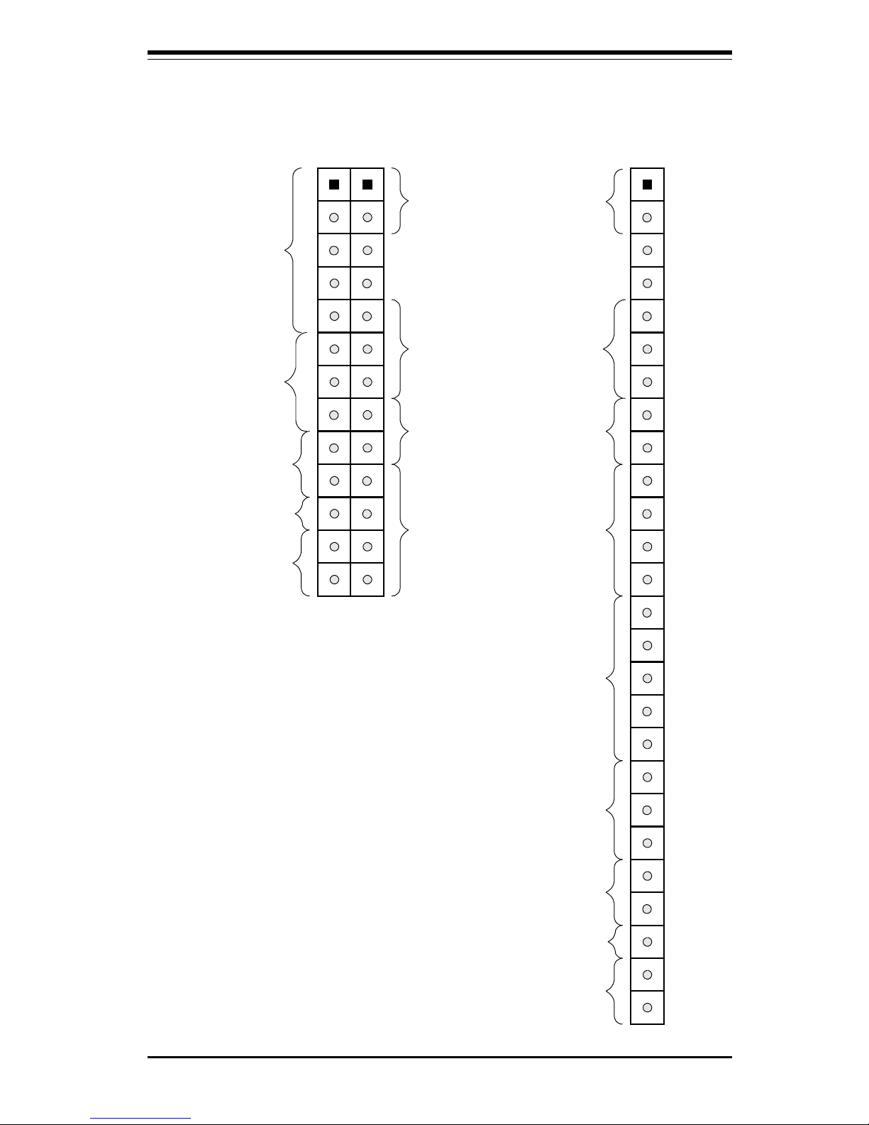
ix
SUPER P6DBS/P6DBE/P6DBU/P6SBU/P6SBS/P6SBA User’s Manual
Front Control Panel Connector
Please see pages 2-9 and 210 for pin definitions.
Hard Drive
LED
Keyboard
lock
Speaker
IR Com
Power
LED
Power On
Reset
JF1
JF2
X
X
Hard
Drive
LED
Keyboard
lock
Speaker
IR Con
Power On
X
Reset
JF2 JF1
X
Power
LED
1
11

Chapter 1: Introduction
1-1
Chapter 1
Introduction
1-1 Overview
The SUPER P6DBS/P6DBE/P6DBU/P6SBU/P6SBS/P6SBA/P6SBM supports
Pentium II 233/266/300/333 MHz and *Celeron 266/300 or higher processors at
a 66MHz bus speed or Pentium II 350/400 MHz processors at a 100MHz bus
speed. The SUPER P6DBU/P6DBS/P6DBE supports dual Pentium II processors, while the SUPER P6SBU/P6SBS/P6SBA/P6SBM supports a single
Pentium II processor. All seven motherboards are based on Intel’s 440BX
chipset, which enables 66/100 MHz system bus speed, Accelerated Graphics
Port (AGP), Wake-on-LAN, SDRAM, concurrent PCI and Ultra DMA 33 MB/s
burst data transfer rate.
While all of the motherboards are ATX form factor, the P6DBU and P6DBE have
5 PCI and 2 ISA with one shared slot. The SUPER P6DBS, P6SBU, P6SBS and
P6SBA have 4 PCI and 3 ISA with one shared slot, and the SUPER P6SBM has
3 PCI and 1 ISA with one shared slot. All seven motherboards have the AGP port,
and all but the P6SBM can accommodate a total of 1 GB EDO at 66 MHz or 512
MB unbuffered SDRAM or 1 GB registered SDRAM memory with 4 168-pin DIMM
sockets. The SUPER P6SBM can accommodate 768 MB registered or 384 MB
unbuffered SDRAM.
AGP reduces contention with the CPU and I/O devices by broadening the bandwidth of graphics to memory. It delivers a maximum of 532 MB/s 2x transfer
mode which is quadruple the PCI speed!
Wake-On-LAN allows remote network management and configuration of the PC,
even in off-hours when the PC is turned off. This reduces the complexity of
managing the network.
Other features that maximize customer satisfaction and simplicity in managing
the computer are PC 98-ready and support for Advanced Configuration and Power
Interface (ACPI). With PC Health Monitoring, you can protect your system from
problems before they even occur.
*Note: Celeron is single processor only
** See bottom of page 2

SUPER P6DBS/P6DBE/P6DBU/P6SBU/P6SBS/P6SBA/P6SBM Manual
1-2
Included I/O on all motherboards are 2 EIDE ports, a floppy port, an ECP/EPP
parallel port, a PS/2 mouse and PS/2 keyboard, 2 serial ports, an infrared port
and 2 USB ports. The SUPER P6DBU and P6SBU provide on-board Adaptec
7890 Ultra II SCSI controller with data transfer rate of up to 80 MB/s, and optional
RAIDport III (ARO-1130xA-2)**. The SUPER P6DBS and P6SBS have an integrated on-board Adaptec 7895 MultiChannel UW SCSI controller. The dual channels allow a data transfer rate of 40 MB/s per channel. Additionally, these two
motherboards have a RAID port on-board to support the Adaptec ARO-1130xA
RAIDport II card** for increased I/O performance and fault tolerance.
**The x in 1130 xA and 1130 xA-2 refers to the RAIDport workstation driver (1130 CA) or server driver
(1130 SA) depending on software used. Please note: 1130 xA is compatible with NT Workstation, NT
Server and Netware Server. The 1130 xA-2 is only compatible with NT Workstation at this time. Check the
Adaptec web site for further information: www.adaptec.com.

Chapter 1: Introduction
1-3
Notes

SUPER P6DBS/P6DBE/P6DBU/P6SBU/P6SBS/P6SBA/P6SBM Manual
1-4
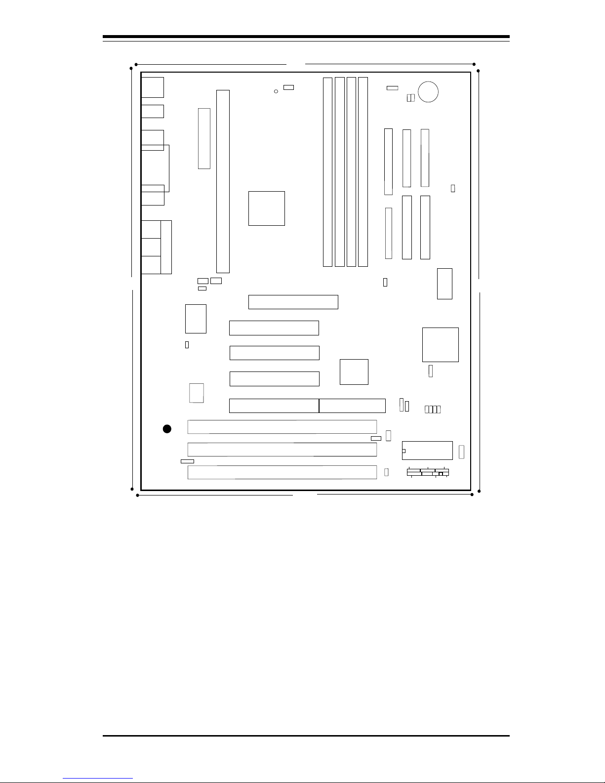
SUPER P6DBS
Figure 1-1. SUPER P6DBS Motherboard Image
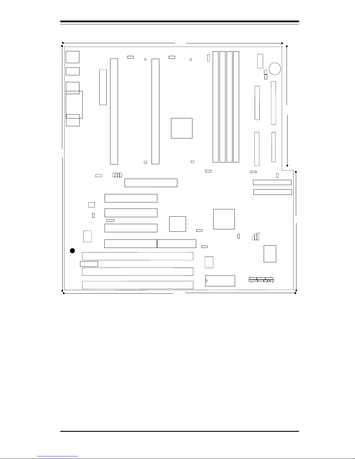
Chapter 1: Introduction
1-5
®
J21
COM2
J20
COM1
J34
PS/2 KB
PS/2 MOUSE
J32
ATX POWER
J9
J11
J12
1
J10
PW_ON
RESET
JF1
IDE LED/KEYLOCK/SPEAKER
IR CON
JF2
Bank3
FLO
P
PY
U
38
U
14
J8
1
J17, J18
USB
CPU 1
FAN
J2
J1
1
CPU 2
FAN
JT2
JT1
U2
Bank0
Bank1
Bank2
JT3
1
J22
1
ULTRA SCSI
JA1
1
BIOS
JB
T2
JBT1
JA6
1
BT2
B
A
T
T
E
R
Y
+
-
1
SCSI LED
WOL
UA1
JA4
PCI 1
PCI 2
PCI 3
PCI 4
RAID PORT
U48
JL1
Chassis
Intrusion
A
G
P
P
O
R
T
1
JP20
JB
1
JB2
JB3
JB4
U37
U15
JA5
JA5, JA6:
SCSI Termination
JBT1: CMOS Clear
JBT2: Ext Battery
JP11
UW SCSI
——–—— Manufacturer Settings —–———
JBT1: 1-2 (default)
2-3 CMOS Clear
* To clear the CMOS completely,
disconnect the power source.
JL1: OFF (default)
ON (intrusion)
JP11: 1-2 Auto
2-3 66 MHz
OFF 100 MHz
JP20: 1-2 PIIX CTL PD State
2-3 BIOS CTL PD State (default)
WOL: Wake-on-LAN
——–———————–——–—–——–——–—
JTM
PIIX4E
BX
J19
Parallel
Port
Figure 1-2. SUPER P6DBS Motherboard Layout
SUPER P6DBS
—————Pentium II CPU Speed–————
JB1 JB2 JB3 JB4
x3 ON OFF ON ON
x3.5 OFF OFF ON ON
x 4 ON ON OFF ON
x4.5 OFF ON OFF ON
x 5 ON O FF OF F ON
x5.5 OFF OFF OFF ON
x 6 ON ON ON OFF
——–—–————————————————
*Note: To Enable Overheat Buzzer place a
jumper on BZ_On.
6"
6"
12"
9.65"
10.65"
ID
E 1
J15
1
IDE 2
J16
1
JA2
1
UW SCSI
BZ_ON
JOH
Overheat LED
PWR_SEC
1
J36
BZ
1
JA3
1
JA7
1
JP18
J13
J14
JJ14
SBLINK
1

SUPER P6DBS/P6DBE/P6DBU/P6SBU/P6SBS/P6SBA/P6SBM Manual
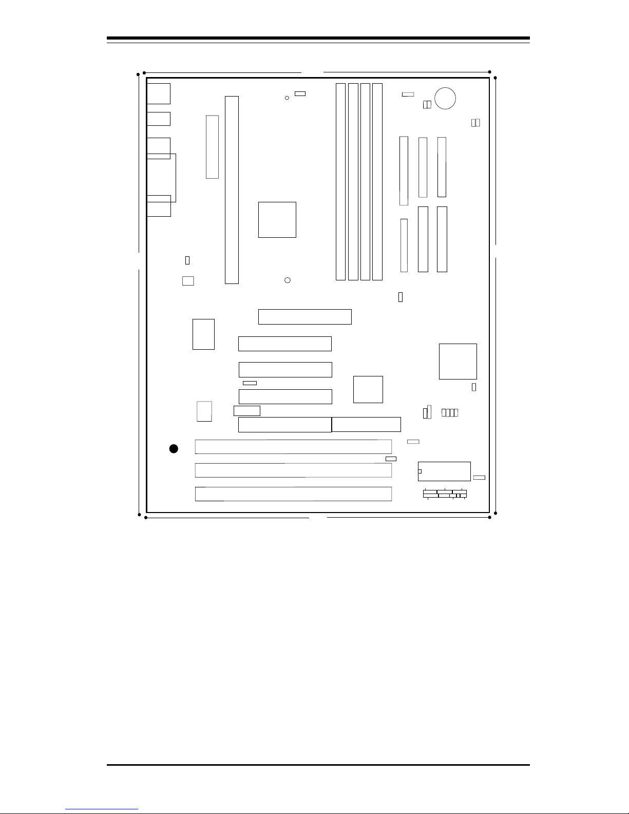
1-6
SUPER P6DBE
Figure 1-3. SUPER P6DBE Motherboard Image
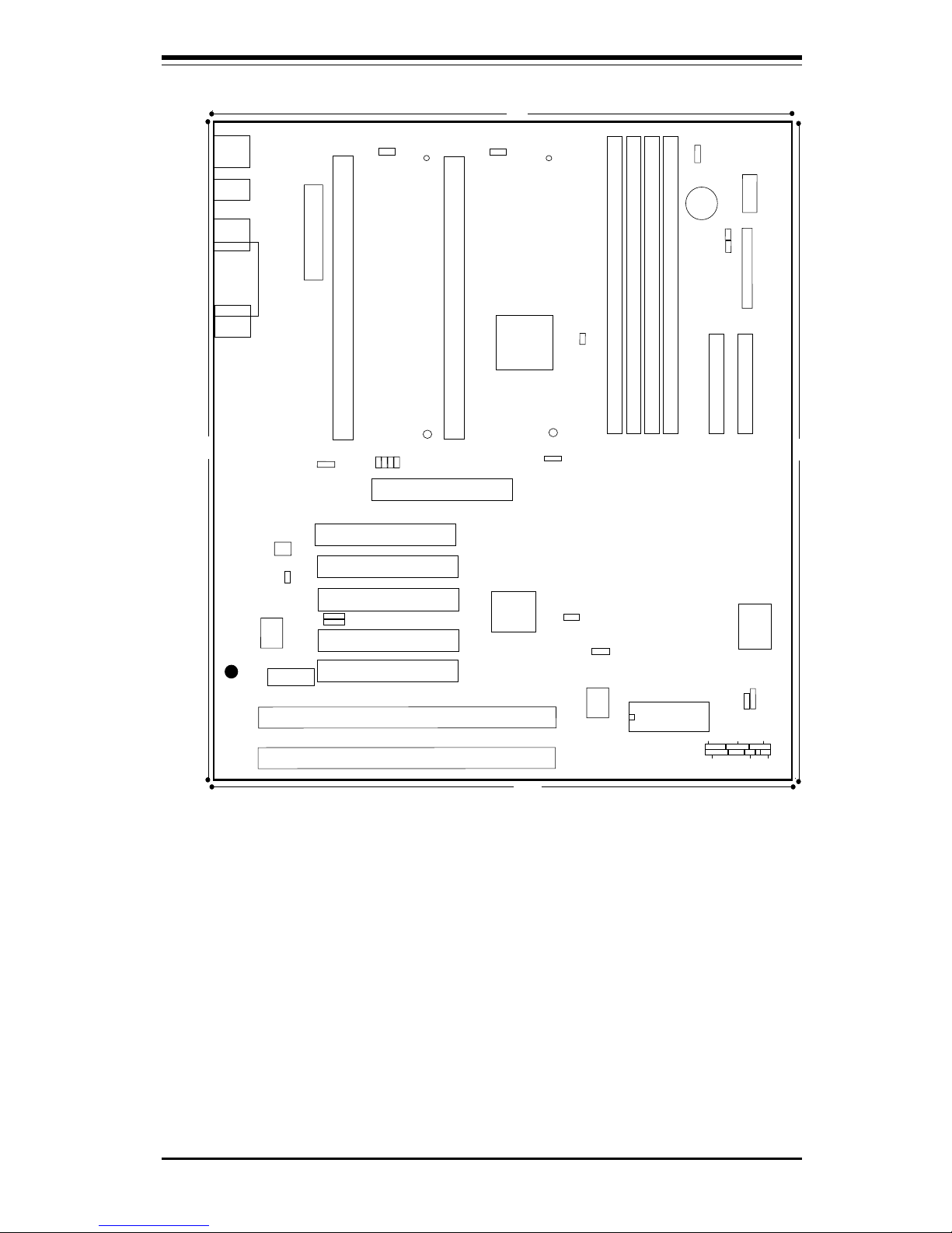
Chapter 1: Introduction
1-7
®
J19
Parallel
Port
J21
COM2
J20
COM1
J13
J34
PS/2 KB
PS/2 MOUSE
J32
ATX POWER
PW_ON
RESET
JF1
IDE LED/KEYLOCK/SPEAKER
IR CON
JF2
Bank3
IDE 2
ID
E 1
FLO
P
PY
U
38
U
14
J8
1
J17, J18
USB
CPU 1
FAN
J2
J1
1
CPU 2
FAN
JT2
JT1
U2
Bank0
B
ank1
Bank2
JT3
T
he
rm
a
l
C
o
ntrol F
an
1
J15 J16
1
1
BIOS
1
BT2
B
A
T
T
E
R
Y
+
-
1
WOL
PCI 1
PCI 2
PCI 3
PCI 4
U48
JL1
Chassis
Intrusion
A
G
P
P
O
R
T
1
JP20
JB
1
JB2
JB3
JB4
U37
U15
JBT1: CMOS Clear
JBT2: Ext Battery
JP11
——–—— Manufacturer Settings —–———
JBT1: 1-2 (default)
2-3 CMOS Clear
To clear the CMOS completely,
disconnect the power source.
JL1: OFF (default)
ON (intrusion)
JP11: 1-2 Auto
2-3 66 MHz
OFF 100 MHz
JP20: 1-2 PIIX CTL PD State
2-3 BIOS CTL PD State (default)
WOL: Wake-on-LAN
——–—–——————–———–——–——–—
BX
PIIX4E
Figure 1-4. SUPER P6DBE Motherboard Layout
SUPER P6DBE
*Note: To Enable Overheat Buzzer place a
jumper on BZ_On.
—————Pentium II CPU Speed–————
JB1 JB2 JB3 JB4
x3 ON OFF ON ON
x3.5 OFF OFF ON ON
x 4 ON ON OFF ON
x4.5 OFF ON OFF ON
x5 ON OFF OFF ON
x5.5 OFF OFF OFF ON
x 6 ON ON ON OFF
——–—–————————————————
J22
BZ_ON
JP16
J
B
T
2
JBT1
JP18
PCI 5
J35
J9
J10
J11
J12
BZ
PWR_SEC
J14
9.6"
9.6"
12"
12"
J36
1
Overheat LED
JOH1
1
SBLINK
1
JL2
1
1
JTM

SUPER P6DBS/P6DBE/P6DBU/P6SBU/P6SBS/P6SBA/P6SBM Manual
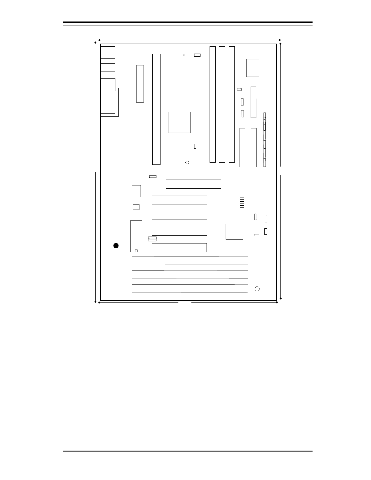
1-8
SUPER P6DBU
Figure 1-5. SUPER P6DBU Motherboard Image
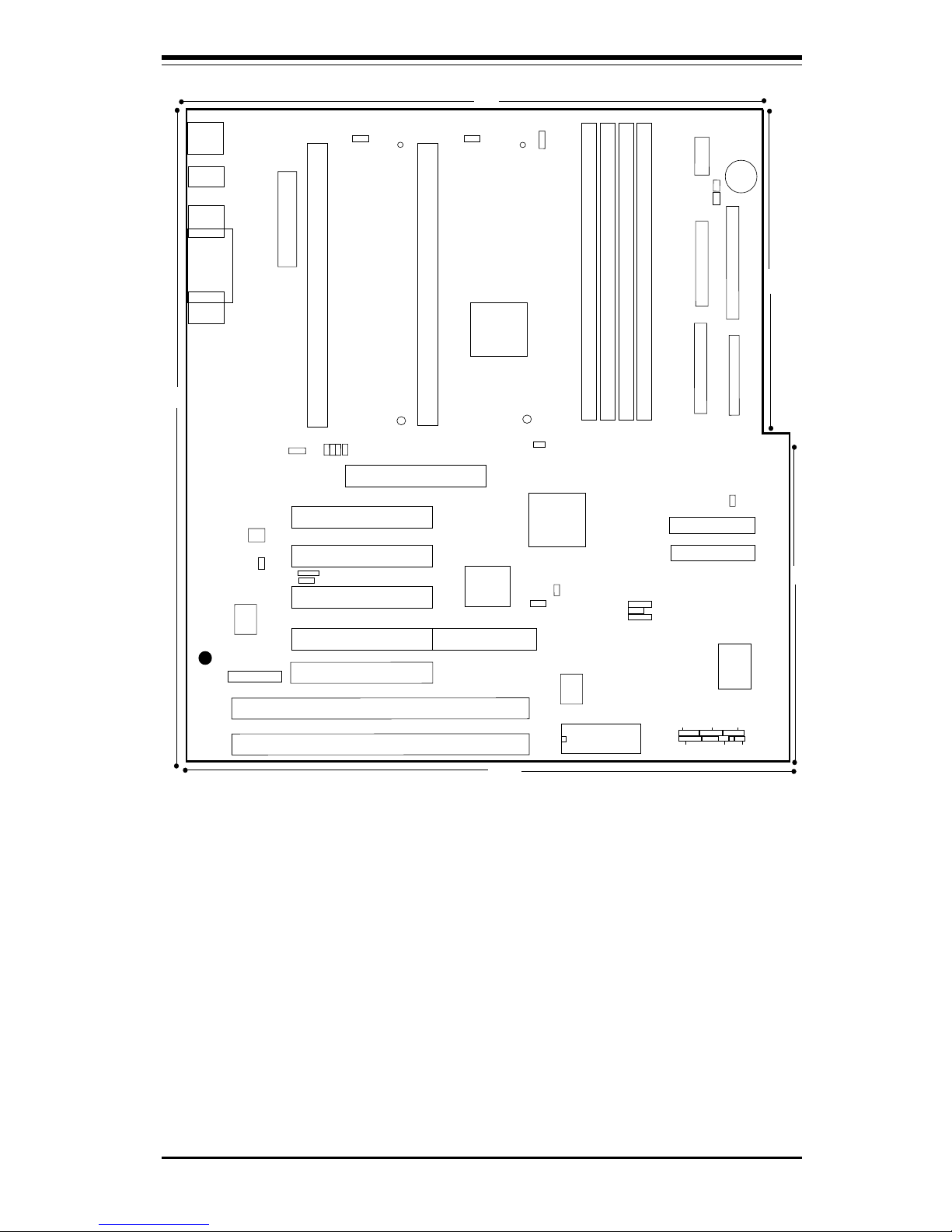
Chapter 1: Introduction
1-9
Figure 1-6. SUPER P6DBU Motherboard Layout
®
J21
COM2
J20
COM1
J14
J13
J34
PS/2 KB
PS/2 MOUSE
J32
ATX POWER
J9
J11
J12
J10
PW_ON
RESET
JF1
IDE LED/KEYLOCK/SPEAKER
IR CON
JF2
B
ank3
U38
U14
J8
1
J17, J18
USB
CPU 1
FAN
J2
J1
1
CPU 2
FAN
JT2
JT1
U2
Bank0
Bank1
B
ank2
ULTRA SCSI
JA1
BIOS
BT2
B
A
T
T
E
R
Y
+
-
UA1
JA4
PCI 1
PCI 2
PCI 3
PCI 4
RAID PORT
U48
JL1
Chassis
Intrusion
A
G
P
P
O
R
T
U37
U15
JBT1: CMOS Clear
JBT2: Ext Battery
JP11
UW SCSI
Ultra II LVD/SE
SUPER P6DBU
——–—— Manufacturer Settings —–———
JBT1: 1-2 (default)
2-3 CMOS Clear
* To clear the CMOS completely,
disconnect the power source.
JL1: OFF (default)
ON (intrusion)
JP11: 1-2 Auto
2-3 66 MHz
OFF 100 MHz
JP20: 1-2 PIIX CTL PD State
2-3 BIOS CTL PD State (default)
WOL: Wake-on-LAN
S-TERM: On: SCSI Termination Enable
Off: Termination Disable
——–———————–——–—–——–——–—
PIIX4E
BX
J19
Parallel
Port
J35
SBLINK
1
JL2
1
JTM
JB4
JB3
JB2
J
B
1
JP20
1
1
WOL
JP18
1
JA5, JA6:
SCSI Termination
J16
J15
IDE 2
ID
E 1
1
1
1
FLOPPY
J22
1
JBT1
JBT2
SLED
S-TER
M
Note: JA3 is Optional
Note: To Enable Overheat Buzzer place a
jumper on BZ_On.
—————Pentium II CPU Speed–————
JB1 JB2 JB3 JB4
x 3 ON O FF ON ON
x3.5 OFF OFF ON ON
x 4 ON ON OFF ON
x4.5 OFF ON OFF ON
x5 ON OFF OFF ON
x5.5 OFF OFF OFF ON
x 6 ON ON ON OFF
——–—–————————————————
6"
6"
12"
10.65"
9.65"
JT3
T
h
erm
a
l
C
o
ntro
l F
an
1
JA3
1
JA2
BZ_ON
JOH
Overheat LED
PWR_SEC
1
J36
BZ
1

SUPER P6DBS/P6DBE/P6DBU/P6SBU/P6SBS/P6SBA/P6SBM Manual
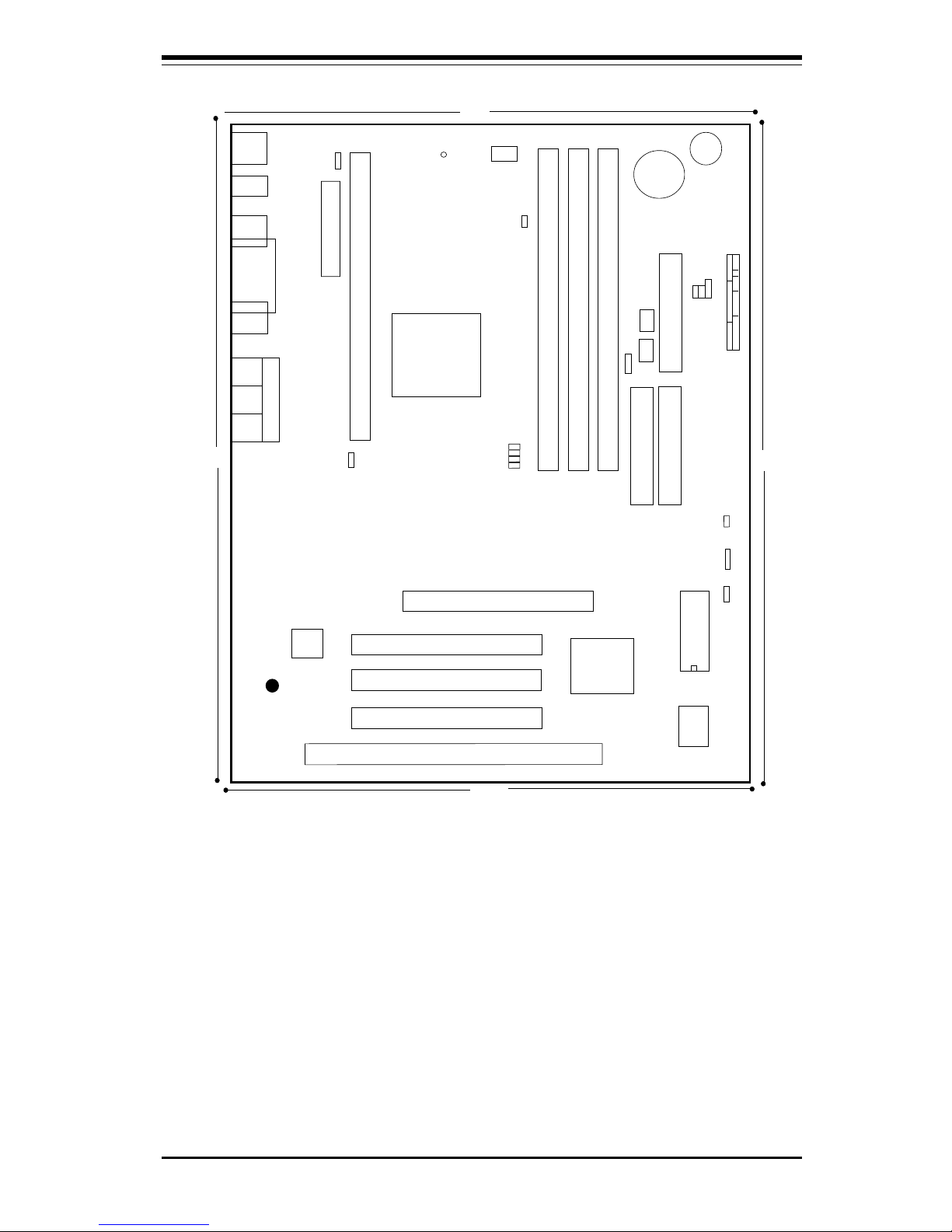
1-10
SUPER P6SBU
Figure 1-7. SUPER P6SBU Motherboard Image
Chapter 1: Introduction
1-11
Figure 1-8. SUPER P6SBU Motherboard Layout
®
J21
COM2
J20
COM1
J34
PS/2 KB
PS/2 MOUSE
J32
ATX POWER
J9
J11
J12
J10
B
ank3
U14
J8
1
J17, J18
USB
CPU FAN
J1
JT1
U2
Bank0
B
ank1
B
ank2
JA4
PCI 1
PCI 2
PCI 3
PCI 4
RAID PORT
A
G
P
P
O
R
T
U56
SUPER P6SBU
JF1
JF2
U38
IR CON PW_ON
RESET
BIOS
IDE LED/KEYLOCK/SPEAKER
1
J22
J16
1
1
ULTRA SCSI
FLO
P
PY
IDE 2
ID
E
1
1
1
1
1
JA3
J15
BZ_ON
JOH
JOH: Overheat LED
JT
3: T
he
rm
al C
o
ntrol F
an
JA5, JA6: SCSI Termination
JTM1
1
WOL
JBT2
JP11
JBT1: CMOS Clear
JBT2: Ext Battery
——–—— Manufacturer Settings —–———
JBT1: 1-2 (default)
2-3 CMOS Clear
To clear the CMOS completely,
disconnect the power source.
JL1: OFF (default)
ON (intrusion)
JP11: 1-2 Auto
2-3 66 MHz
OFF 100 MHz
JP20: 1-2 PIIX CTL PD State
2-3 BIOS CTL PD State (default)
WOL: Wake-on-LAN
S-TERM: On: SCSI Termination Enable
Off: Termination Disable
——–———–————–———–——–——–—
—————Pentium II CPU Speed–————
JB1 JB2 JB3 JB4
x 3 ON O FF ON ON
x3.5 OFF OFF ON ON
x 4 ON ON OFF ON
x4.5 OFF ON OFF ON
x5 ON OFF OFF ON
x5.5 OFF OFF OFF ON
x 6 ON ON ON OFF
——–—–————————————————
Note: JA3 is Optional
Note: To Enable Overheat Buzzer place a
jumper on BZ_On.
BZ
JT3
PIIX4E
BX
J19
Parallel
Port
UA10
JB1
JB2
JB3
JB4
1
JBT1
1
JP20
1
3860
JT2
1
SCSI LED
JL1
S-TERM
J37
J44
ESS
1938
7890
JJ14
J14
J13
1
JPSI
12"
12"
8.875"
8.875"
J39
J35
JA1
JA2
UW SCSI
Ultra II LVD/SE

SUPER P6DBS/P6DBE/P6DBU/P6SBU/P6SBS/P6SBA/P6SBM Manual
1-12
SUPER P6SBS
Figure 1-9. SUPER P6SBS Motherboard Image
Chapter 1: Introduction
1-13
Figure 1-10. SUPER P6SBS Motherboard Layout
®
J21
COM2
J20
COM1
JJ14
J14
J13
J34
PS/2 KB
PS/2 MOUSE
J32
ATX POWER
J9
J11
J12
J10
B
ank3
U14
J8
1
J17, J18
USB
CPU FAN
J1
JT1
U2
Bank0
B
ank1
B
ank2
UA1
JA4
PCI 1
PCI 2
PCI 3
PCI 4
RAID PORT
U48
A
G
P
P
O
R
T
1
JP20
JB2
JB3
U56
SUPER P6SBS
JF1
JF2
U38
IR CON
PW_ON
RESET
BIOS
IDE LED/KEYLOCK/SPEAKER
1
JT2
1
J22
J16
1
1
ULTRA SCSI
UW SCSI
UW SCSI
FLO
P
PY
IDE 2
ID
E
1
1
1
JA1 JA2
11
JA3
J15
JA6
JA5
BZ_ON
JOH
JOH: Overheat LED
JT
3: T
herm
al C
o
ntrol F
an
JA5, JA6: SCSI Termination
1 JTM
1
WOL
BT2
B
A
T
T
E
R
Y
+
-
Chassis
Intrusion
JL1
JBT2
JBT1
1
1
JB
1
JB4
SCSI LED
JP11
JBT1: CMOS Clear
JBT2: Ext Battery
——–—— Manufacturer Settings —–———
JBT1: 1-2 (default)
2-3 CMOS Clear
To clear the CMOS completely,
disconnect the power source.
JL1: OFF (default)
ON (intrusion)
JP11: 1-2 Auto
2-3 66 MHz
OFF 100 MHz
JP20: 1-2 PIIX CTL PD State
2-3 BIOS CTL PD State (default)
WOL: Wake-on-LAN
——–———–————–———–——–——–—
—————Pentium II CPU Speed–————
JB1 JB2 JB3 JB4
x 3 ON O FF ON ON
x3.5 OFF OFF ON ON
x 4 ON ON OFF ON
x4.5 OFF ON OFF ON
x5 ON OFF OFF ON
x5.5 OFF OFF OFF ON
x 6 ON ON ON OFF
——–—–————————————————
*Note: To Enable Overheat Buzzer place a
jumper on BZ_On.
BZ
JT3
PIIX4E
BX
J19
Parallel
Port
12"
12"
8.875"
8.875"
SBLINK
1

SUPER P6DBS/P6DBE/P6DBU/P6SBU/P6SBS/P6SBA/P6SBM Manual
1-14
SUPER P6SBA
Figure 1-11. SUPER P6SBA Motherboard Image
Chapter 1: Introduction
1-15
Figure 1-12. SUPER P6SBA Motherboard Layout
J9
J11
J12
J10
J8
Bank0
B
ank1
B
ank2
BT2
PCI 1
PCI 4
U34
A
G
P
P
O
R
T
1
JP20
U27
ATX POWER
J1
PCI 3
J22
J32
J17, J18
USB
J21
COM2
J20
COM1
BIOS
JJ14
J14
J13
U29
1
1
JBT2
JF1
IDE
LED
KEY
LOCK
SPEAKER
JF2
RESET
®
1
+
-
B
A
T
T
E
R
Y
1
1
JBT1
J16 J15
IDE 2
ID
E
1
FLO
PPY
1
JT2
JT3
1
1
+
JOH
WOL
1
JB4
JB2
JB3
JL1
JB1
U14
IR
CON
PW_
ON
JOH: Overheat LED
JL1: Chassis Intrusion
JBT1: CMOS Clear
JBT2: Ext Battery
JP11
U9
CPU FAN
JT1
1
J34
PS/2 KB
PS/2 MOUSE
SUPER P6SBA
PCI 2
——–—— Manufacturer Settings —–———
JBT1: 1-2 (default)
2-3 CMOS Clear
To clear the CMOS completely,
disconnect the power source.
JL1: OFF (default)
ON (intrusion)
JP11: 1-2 Auto
2-3 66 MHz
OFF 100 MHz
JP20: 1-2 PIIX CTL PD State
2-3 BIOS CTL PD State (default)
WOL: Wake-on-LAN
——–———————–———–—–—–——–—
PIIX4E
BX
J19
Parallel
Port
—————Pentium II CPU Speed–————
JB1 JB2 JB3 JB4
x3 ON OFF ON ON
x3.5 OFF OFF ON ON
x 4 ON ON OFF ON
x4.5 OFF ON OFF ON
x 5 ON O FF OF F ON
x5.5 OFF OFF OFF ON
x 6 ON ON ON OFF
——–—–————————————————
12"
12"
7"
7"
SW2
1
1
JL2
JTM
PW-LED

SUPER P6DBS/P6DBE/P6DBU/P6SBU/P6SBS/P6SBA/P6SBM Manual
1-16
SUPER P6SBM
Figure 1-13. SUPER P6SBM Motherboard Image
Chapter 1: Introduction
1-17
Figure 1-14. SUPER P6SBM Motherboard Layout
®
J20
COM1
J21
COM2
J34
PS/2KB
PS/2
MOUSE
J32
ATX POWER
J11
J12
J10
U14
1
J17,
J18
USB
CPU FAN
J1
JT1
U9
Bank0
Bank1
Bank2
PCI 1
PCI 2
PCI 3
A
G
P
P
O
R
T
U59
JF1
JF2
U29
IR CON PW_ON
RESET
BIOS
IDE LED/KEYLOCK/SPEAKER
1
J22
J16
FLO
P
P
Y
IDE2
ID
E
1
1
1
J15
BZ_ON
JOH
JOH: Overheat LED
JT
3: T
herm
al C
on
trol F
an
JTM
1
WOL
JP11
JBT1: CMOS Clear
BZ1
JT2
PIIX4E
BX
J19
Parallel
Port
JB1
JB2
JB3
JB4
JBT1
JP20
1
JL1
J36
J8
JJ14
1
9.6"
8.050"
J4
J5 J6
BATTERY
JP12
JT3
BT2
U27
JPWAKE
1
1
——–—— Manufacturer Settings —–———
JBT1: 1-2 (default)
2-3 Clear CMOS
To clear CMOS completely,
disconnect the power source.
JL1: OFF (default)
ON (intrusion)
JP11: 1-2 Auto
2-3 66 MHz
OFF 100 MHz
JP2 0 : 1-2 PIIX CTL PD State
2-3 BIOS CTL PD State (default)
WOL: Wake-On-LAN
——–———–————–———–——–——–—
—————Pentium II CPU Speed–————
JB1 JB2 JB3 JB4
x3 ON OFF ON ON
x3.5 OFF OFF ON ON
x4 ON ON OFF ON
x4.5 OFF ON OFF ON
x 5 ON OFF OFF ON
x5.5 OFF OFF OFF ON
x6 ON ON ON OFF
——–—–————————————————
AUDIO
1938
SUPER P6SBM
1
1
1
1
1
1
1
1
1
1
SUPER P6DBS/P6DBE/P6DBU/P6SBU/P6SBS/P6SBA/P6SBM Manual
1-18
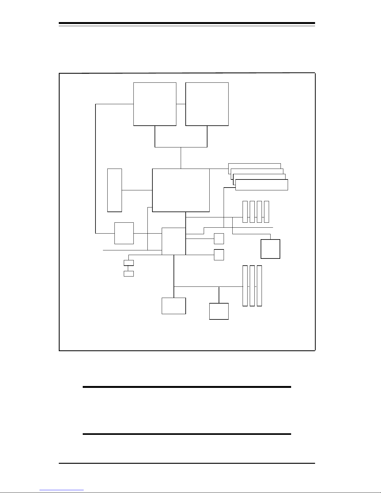
CPU
440BX
CPU
AGP
Port
IO
APIC
PIIX4E
Power
Mana
g
ement
SDRAM
Host Bus
PCI Slots
SMBus
USB
Ports
USB
IDE Ports
ISA Slots
BIOS
SIO
SCSI
Figure 1-15. 440BX AGP SET:
System Block Diagram (Dual Processors)
NOTE: This is a general block diagram and may not
represent the number of slots/CPUs on your motherboard.
See the following page for the actual specifications of each
motherboard.
Chapter 1: Introduction
1-19
Features of P6DBS, P6DBE, P6DBU, P6SBU, P6SBS,
P6SBA and P6SBM Motherboards*
* Bold text denotes variations in features.
The following list covers the general features of the SUPER P6DBS, P6DBE,
P6DBU, P6SBU, P6SBS, P6SBA and P6SBM motherboards.
CPU
• Dual Pentium II 233/266/300/333 MHz processor at 66 MHz bus speed or
350/400 MHz at 100 MHz bus speed (Note: SUPER P6SBU, P6SBS, P6SBA and
P6SBM support a single Pentium II processor.)
Memory
• 1 GB EDO at 66 MHz or 512 MB unbuffered 3.3V SDRAM or 1 GB
registered SDRAM (P6DBS/P6DBE/P6DBU/P6SBU/P6SBS only)
• 768 MB EDO, 768 MB registered DIMM, 384 MB SDRAM (P6SBA and P6SBM
only)
(Note: When the CPU bus is running at 100 MHz, the SDRAM must be PC-100 compliant
DIMMs)
(Note: The maximum memory cacheability size depends on the processor capabilities.)
• Error Checking and Correction and Error Checking support
Chipset
• Intel 440BX
Expansion Slots
P6DBS/P6SBU/P6SBS/P6SBA P6DBU/P6DBE P6SBM
• 4 PCI slots • 5 PCI slots • 3 PCI slots
• 3 ISA slots • 2 ISA slots • 1 ISA slot
One shared PCI/ISA slot
• 1 AGP slot • 1 AGP slot • 1 AGP slot
BIOS
• 2 Mb AMI® Flash BIOS
• APM 1.2, DMI 2.01, Plug and Play (PnP)
• Adaptec 7890 SCSI BIOS 2.01 (P6DBU/P6SBU only)
• Adaptec 7895 SCSI BIOS (P6DBS/P6SBS only)
PC Health Monitoring
• Seven on-board voltage monitors for CPU core(s), CPU I/O, +3.3V, ±5V,
and ±12V
• Three-fan status monitors with firmware/software on/off control
• Environment temperature monitor and control
• CPU fan auto-off in sleep mode
• Chassis overheat alarm, LED, and control

SUPER P6DBS/P6DBE/P6DBU/P6SBU/P6SBS/P6SBA/P6SBM Manual
1-20
• Chassis intrusion detection
• System resource alert
• Hardware BIOS virus protection
• Switching voltage regulator for the CPU core
• SUPERMICRO SUPER Doctor and Intel® LANDesk® Client Manager
(LDCM) support
ACPI/PC 98 Features
• Microsoft OnNow
• Slow blinking LED for suspend-state indicator
• BIOS support for USB keyboard
• Real time clock wake-up alarm
• Main switch override mechanism
• External modem ring-on
On-Board I/O
• 68-pin 16-bit Ultra II LVD/SE SCSI connectors and 68-pin, 16 bit Ultra
Wide SCSI Connector / 50-pin 8-bit Ultra SCSI connector (P6DBU/P6SBU
only)
• 68-pin 16-bit Dual Ultra-Wide SCSI connectors and 50-pin 8-bit Ultra SCSI
connector (P6DBS/P6SBS only)
• RAID port for Adaptec ARO-1130xA RAIDport II card (P6DBS/P6SBS only)
• RAID port for Adaptec ARO-1130xA-2 RAIDport III card (P6DBU/P6SBU only)
• 2 EIDE Bus Master interfaces support Ultra DMA/33 and Mode 4
• 1 floppy port interface
• 2 Fast UART 16550 serial ports
• EPP (Enhanced Parallel Port) and ECP (Extended Capabilities Port)
parallel port
• PS/2 mouse and PS/2 keyboard
• Infrared port
• 2 USB (Universal Serial Bus) ports
• Solo-1 PCI
Audio
Drive
®
(Standard on P6SBM, optional on P6SBU)
CD Utilities
• Intel LANDesk Client Manager for Windows NT® and Windows® 95
(optional)
• PIIX4E Upgrade Utility for Windows 95
• BIOS Flash Upgrade Utility
• SUPER Doctor Utility
• SCSI Utility, manual and driver

Chapter 1: Introduction
1-21
Dimensions
• SUPER P6DBS - ATX (12" x 9.65") * See board diagram for full measurements
• SUPER P6DBE - ATX (12" x 9.6")
• SUPER P6DBU - ATX (12" x 9.65") * See board diagram for full measurements
• SUPER P6SBU - ATX (12" x 8.875")
• SUPER P6SBS - ATX (12" x 8.875")
• SUPER P6SBA - ATX (12" x 7")
• SUPER P6SBM - Micro ATX (9.6" x 8.05")
1-2 Chipset Overview
The 440BX chipset, developed by Intel, is the ultimate processor platform targeted for 3D graphics and multimedia applications. Along with System-to-PCI
bridge integrated with optimized DRAM controller and data path, the chipset
introduces the Accelerated Graphics Port (AGP) interface. AGP is a high performance, component level interconnect targeted at 3D applications and is based
on a set of performance enhancements to PCI. The I/O subsystem portion of the
440BX platform is based on the PIIX4E, a highly integrated version of Intel's PCIto-ISA bridge family.
The PCI/AGP and system bus interface controller (82443BX) supports up to two
Pentium II processors. It provides an optimized 72-bit DRAM interface (64-bit
data plus ECC). This interface supports 3.3V DRAM technologies. The controller provides the interface to a PCI bus operating at 33 MHz. This interface
implementation is compliant with the PCI Rev 2.1 Specification. The AGP interface is based on the AGP Specification Rev 1.0. It can support up to 133 MHz
(532 MB/s) data transfer rates.
1-3 PC Health Monitoring
This section describes the PC health monitoring features of the SUPER P6DBU/
P6DBS/P6DBE/P6SBU/P6SBS/P6SBA/P6SBM. All have an on-board System
Hardware Monitor chip that supports PC health monitoring.
 Loading...