


®
SUPER P3TDL3
SUPER P3TDLE
USER’S MANUAL
Revision 1.0c
SUPER

The information in this User’s Manual has been carefully reviewed and is believed to be
accurate. The vendor assumes no responsibility for any inaccuracies that may be contained
in this document, makes no commitment to update or to keep current the information in this
manual, or to notify any person or organization of the updates.
Please Note: For the
most up-to-date version of this manual, please see our web site at
www.supermicro.com.
SUPERMICRO COMPUTER reserves the right to make changes to the product described in
this manual at any time and without notice. This product, including software, if any, and
documentation may not, in whole or in part, be copied, photocopied, reproduced, translated or
reduced to any medium or machine without prior written consent.
IN NO EVENT WILL SUPERMICRO COMPUTER BE LIABLE FOR DIRECT, INDIRECT,
SPECIAL, INCIDENTAL, OR CONSEQUENTIAL DAMAGES ARISING FROM THE USE OR
INABILITY TO USE THIS PRODUCT OR DOCUMENTATION, EVEN IF ADVISED OF THE
POSSIBILITY OF SUCH DAMAGES. IN PARTICULAR, THE VENDOR SHALL NOT HAVE
LIABILITY FOR ANY HARDWARE, SOFTWARE, OR DATA STORED OR USED WITH THE
PRODUCT, INCLUDING THE COSTS OF REPAIRING, REPLACING, INTEGRATING,
INSTALLING OR RECOVERING SUCH HARDWARE, SOFTWARE, OR DATA.
Any disputes arising between manufacturer and customer shall be governed by the laws of
Santa Clara County in the State of California, USA. The State of California, County of Santa
Clara shall be the exclusive venue for the resolution of any such disputes. Supermicro's total
liability for all claims will not exceed the price paid for the hardware product.
Unless you request and receive written permission from SUPER MICRO COMPUTER, you
may not copy any part of this document.
Information in this document is subject to change without notice. Other products and
companies referred to herein are trademarks or registered trademarks of their respective
companies or mark holders.
Copyright © 2002 by SUPER MICRO COMPUTER INC.
All rights reserved.
Printed in the United States of America

Preface
About This Manual
This manual is written for system integrators, PC technicians and
knowledgeable PC users. It provides information for the installation and use
of the SUPER P3TDL3/P3TDLE motherboard. The SUPER P3TDL3/P3TDLE
supports single Intel® PentiumTM III FCPGA 500 MHz-1.4 GHz processors,
including low power PentiumTM III processors, at front side bus speeds of
133 and 100 MHz. Please refer to the support section of our web site
(http://www.supermicro.com/TechSupport.htm) for a complete listing of
supported processors. Intel® FCPGA processors are housed in a 370-pin
package.
Manual Organization
Chapter 1 includes a checklist of what should be included in your
mainboard box, describes the features, specifications and performance of
the SUPER P3TDL3/P3TDLE mainboard and provides detailed information
about the chipset.
Chapter 2 begins with instructions on handling static-sensitive devices.
Read this chapter when you want to install the processor and DIMM memory
modules and when mounting the mainboard in the chassis. Also refer to
this chapter to connect the floppy and hard disk drives, SCSI drives, the IDE
interfaces, the parallel and serial ports and the twisted wires for the power
supply, the reset button, the keylock/power LED, the speaker and the keyboard.
If you encounter any problems, read Chapter 3, which describes troubleshooting procedures for the video, the memory and the setup configuration
stored in CMOS. For quick reference, a general FAQ [Frequently Asked
Questions] section is provided. Instructions are also included for contacting technical support. In addition, you can visit our web site at:
www.supermicro.com/techsupport.htm for more detailed information.
Chapter 4 includes an introduction to BIOS and provides detailed information on running the CMOS Setup utility.
Appendix A gives information on BIOS error beep codes and messages.
Appendix B provides POST diagnostic error messages.
iii
Preface

SUPER P3TDL3/P3TDLE User’s Manual
iv
Table of Contents
Preface
About This Manual ...................................................................................................... ii i
Manual Organization ................................................................................................... iii
Chapter 1: Introduction
1-1 Overview ......................................................................................................... 1-1
Checklist .................................................................................................... 1 - 1
Contacting Supermicro ............................................................................ 1 -2
SUPER P3TDL3 Image ............................................................................. 1-4
SUPER P3TDLE Image ............................................................................. 1-5
SUPER P3TDL3 Layout............................................................................ 1-6
SUPER P3TDL3 Quick Reference........................................................... 1-7
SUPER P3TDLE Layout............................................................................ 1-8
SUPER P3TDLE Quick Reference........................................................... 1-9
Server Works LE Chipset: System Block Diagram ........................... 1-10
Features of the P3TDL3/P3TDLE Motherboard ................................. 1-11
1-2 Chipset Overview......................................................................................... 1-12
1-3 Special Features........................................................................................... 1-1 3
BIOS Recovery ....................................................................................... 1-1 3
Recovery from AC Power Loss ......................................................... 1-13
1-4 PC Health Monitoring.................................................................................... 1-14
1-5 ACPI/PC 98 Features ................................................................................... 1-15
1-6 Power Supply ............................................................................................... 1-17
1- 7 Super I/O......................................................................................................... 1-17
Chapter 2: Installation
2-1 Static-Sensitive Devices ............................................................................... 2-1
Precautions ............................................................................................... 2-1
Unpacking.................................................................................................. 2-1
2- 2 FCPGA Processor Installation ...................................................................... 2-2
2-3 Mounting the Motherboard in the Chassis ................................................. 2-3
2-4 Installing DIMMs............................................................................................... 2-4
2- 5 Port/Control Panel Connector Locations ..................................................... 2-6
2-6 Connecting Cables ......................................................................................... 2-7
Power Supply Connector ....................................................................... 2-7
Secondary Power Connector................................................................. 2-7
Power LED ................................................................................................. 2 -8
IDE LED ...................................................................................................... 2-8

PWR_ON .................................................................................................... 2-8
NIC_LED ..................................................................................................... 2-8
Reset .......................................................................................................... 2-8
Sleep ........................................................................................................... 2 -9
Non-Maskable Interrupt .......................................................................... 2 -9
Extra Universal Serial Bus Connection (USB3) .................................. 2-9
5 Volt StandBy ....................................................................................... 2-9
Fan Fail LED............................................................................................. 2-10
Power Fail LED ....................................................................................... 2-10
NIC LED..................................................................................................... 2-10
I2C .............................................................................................................. 2-10
Chassis Intrusion ................................................................................... 2-10
Keyboard Lock ....................................................................................... 2-11
Overheat LED ......................................................................................... 2-11
Speaker ................................................................................................... 2-11
Fan Headers ............................................................................................ 2-11
Universal Serial Bus Connector .......................................................... 2-11
Wake-On-LAN ......................................................................................... 2-12
Wake-On-Modem .................................................................................... 2-12
Power Supply Fail Header .................................................................... 2-12
SLED1 (SCSI LED) Indicator................................................................. 2-12
Ethernet Port........................................................................................... 2-13
Serial Ports ............................................................................................. 2-13
ATX PS/2 Keyboard and Mouse Ports ................................................ 2-13
2- 7 DIP Switch Settings ..................................................................................... 2-14
DIP Switch 1: Core/Bus Ratio .............................................................. 2-14
2- 8 Jumper Settings ............................................................................................ 2- 15
CMOS Clear............................................................................................. 2-15
SCSI Termination Enable/Disable (P3TDL3 ONLY) ............................2-15
Overheat Alarm Enable/Disable ............................................................2-16
Onboard LAN/NIC Enable/Disable......................................................... 2-16
3rd Power Supply Failure Alarm Enable/Disable .............................. 2-16
Watchdog Reset ..................................................................................... 2-16
2- 9 Parallel Port, Floppy/Hard Disk Drive and SCSI Connections ............... 2-17
Parallel Port Connector ......................................................................... 2-17
Floppy Connector ................................................................................... 2-18
IDE Connectors ...................................................................................... 2-18
50-pin Legacy SCSI Connector ............................................................ 2-19
Ultra Wide SCSI Connector ................................................................... 2-19
v
Table of Contents

Ultra160 SCSI Connector.......................................................................2-20
2-10 Installing Software Drivers......................................................................... 2-21
Chapter 3: Troubleshooting
3-1 Troubleshooting Procedures ......................................................................... 3- 1
Before Power On ...................................................................................... 3 -1
No Power ................................................................................................... 3-1
No Video ................................................................................................... 3-1
Memory Errors .......................................................................................... 3-2
Losing the System’s Setup Configuration ........................................... 3-2
3-2 Technical Support Procedures .................................................................... 3-2
3-3 Frequently Asked Questions........................................................................ 3-3
3-4 Returning Merchandise for Service............................................................ 3-5
Chapter 4: BIOS
4-1 Introduction....................................................................................................... 4 -1
4-2 BIOS Features ................................................................................................. 4- 2
4-3 Running Setup ................................................................................................. 4- 2
Main BIOS Setup Menu ........................................................................... 4 -3
4-4 Advanced BIOS Setup .................................................................................... 4-4
4-5 Chipset Setup ................................................................................................. 4-15
4-6 PCI PnP Setup ............................................................................................... 4-17
4-7 Power Setup ................................................................................................... 4-21
4-8 Boot Setup...................................................................................................... 4-24
4-9 Security Setup ................................................................................................ 4-26
4-10 Exit Setup ....................................................................................................... 4-28
Appendices:
Appendix A: BIOS Error Beep Codes and Messages .........................................A- 1
Appendix B: AMIBIOS Post Checkpoint Codes .................................................... B -1
vi
SUPER P3TDL3/P3TDLE User’s Manual

Chapter 1: Introduction
1-1
Introduction
Chapter 1
Introduction
1-1 Overview
Checklist
Congratulations on purchasing your computer motherboard from an acknowledged leader in the industry. Supermicro boards are designed with
the utmost attention to detail to provide you with the highest standards in
quality and performance.
Please check that the following items have all been included with your
motherboard. If anything listed here is damaged or missing, contact your
retailer.
One (1) Supermicro Mainboard
One (1) ribbon cable for IDE devices
One (1) floppy ribbon cable for (1) 5.25-inch floppy and (2) 3.5-inch floppy drives
One (1) I/O backpanel shield
SCSI Accessories (depending on motherboard)
One (1) 50-pin Ultra SCSI cable (P3TDL3 ONLY)
One (1) 68-pin LVD SCSI cable (P3TDL3 ONLY)
One (1) set of SCSI driver diskettes (P3TDL3 ONLY)
One (1) SCSI manual (P3TDL3 ONLY)
One (1) Supermicro CD or diskettes containing drivers and utilities
One (1) BIOS User's Manual

SUPER P3TDL3/P3TDLE User’s Manual
1-2
Introduction
Contacting Supermicro
Headquarters
Address: SuperMicro Computer, Inc.
980 Rock Ave.
San Jose, CA 95131 U.S.A.
Tel: +1 (408) 503-8000
Fax: +1 (408) 503-8008
Email: marketing@supermicro.com (General Information)
support@supermicro.com (Technical Support)
Web Site: www.supermicro.com
Europe
Address: SuperMicro Computer B.V.
Het Sterrenbeeld 28, 5215 ML
's-Hertogenbosch, The Netherlands
Tel: +31 (0) 73-6400390
Fax: +31 (0) 73-6416525
Email: sales@supermicro.nl (General Information)
support@supermicro.nl (Technical Support)
rma@supermicro.nl (Customer Support)
Asia-Pacific
Address: SuperMicro, Taiwan
D5, 4F, No. 16 Chien-Ba Road
Chung-Ho 235, Taipei Hsien, Taiwan, R.O.C.
Tel: +886-(2) 8226-3990
Fax: +886-(2) 8226-3991
Web Site: www.supermicro.com.tw
Technical Support:
Email: support@supermicro.com.tw
Tel: 886-2-8226-3990, ext.132 or 139

Chapter 1: Introduction
1-3
Introduction
Notes

SUPER P3TDL3/P3TDLE User’s Manual
1-4
Introduction
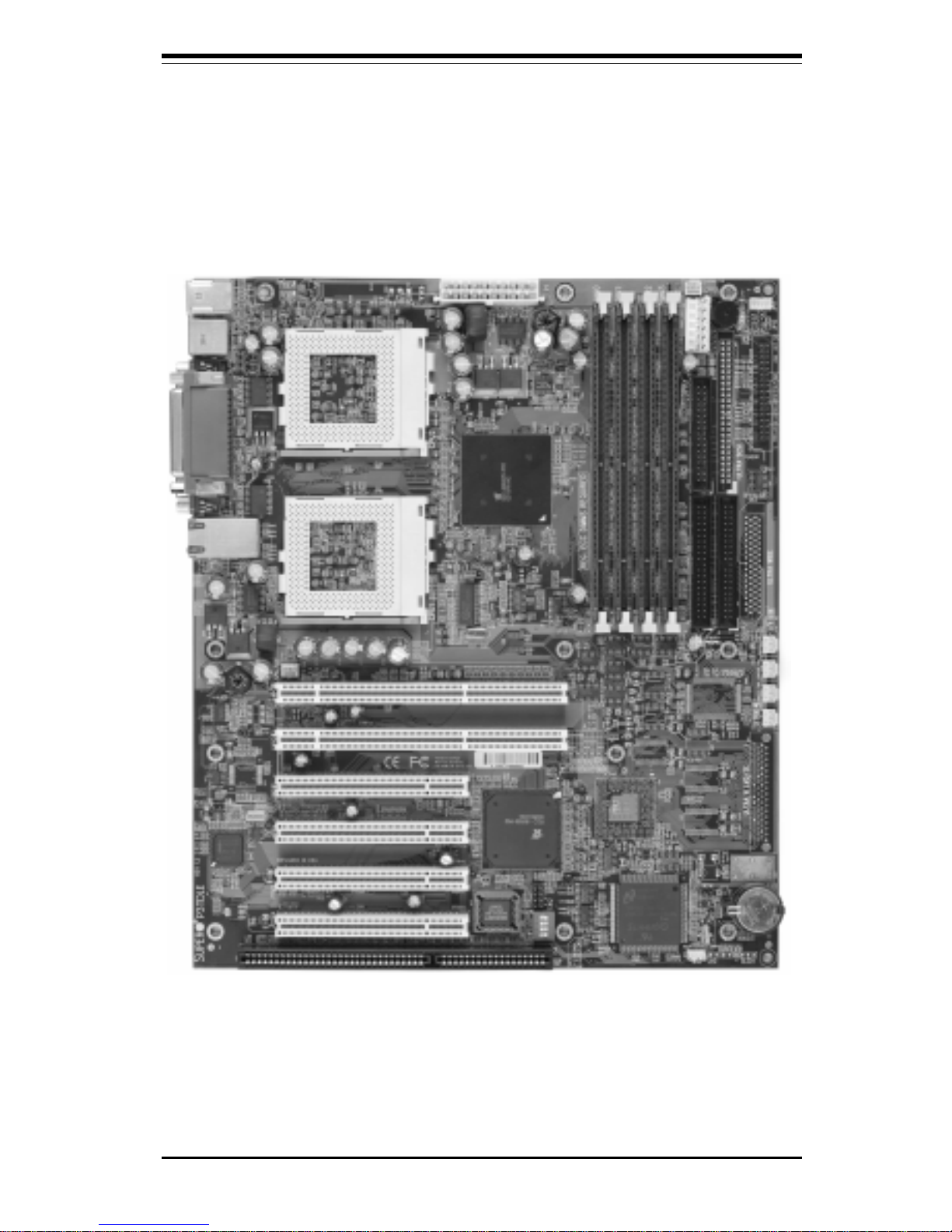
SUPER P3TDL3
Figure 1-1. SUPER P3TDL3 Image
Chapter 1: Introduction
1-5
Introduction
SUPER P3TDLE
Figure 1-2. SUPER P3TDLE
SUPER P3TDL3/P3TDLE User’s Manual
1-6
Introduction
Figure 1-3. SUPER P3TDL3 Layout
(not drawn to scale)
See Chapter 2 for the locations of the I/O ports and for details on
the Front Control Panel (JF1) connector.
J28
KB/
Mouse
J23
USB0/1
COM1
COM2
J27
Parallel Port
J104
Ethernet Port
FCPGA
Processor 1
FCPGA
Processor 2
North
Bridge
DIMM2
DIMM3
DIMM0
DIMM1
IDE #1
IDE #2
ULTRA WIDE SCSI
PWR_SEC
JP12
JF1
J24
JP2
JA4
JP1
JP11
JP7
PCI 3
Thermal Fan
ULTRA SCSI
FLOPPY
USB4
PCI 4
PCI 2
PCI 1
PCI-64 #2
PCI-64 #1
ISA
South
Bridge
AIC-7892
Super I/O BIOS
Battery
ULTRA160 LVD SCSI
JA1
24-PIN ATX POWER U45
JP13
JP4
SW1
JP14
JBT1
WOM
WOL
SLED1
JP8
Chassis Fan 6
Chassis Fan 5
Chassis Fan 4
Chassis Fan 7
SUPER P3TDL3
®
CPU Fan 2
CPU Fan 1

Chapter 1: Introduction
1-7
Introduction
P3TDL3 Quick Reference
Jumpers Description Default Setting
JP1 SCSI Termination Pins 1-2 (Enabled)
JBT1 CMOS Clear (See Section 2-8)
JP2 Front Side Bus Speed Pins 1-2 (Auto)
JP4 Manufacturer's Setting Open
JP7 Overheat Alarm Closed (Enabled)
JP8 LAN Enable/Disable Open (Enabled)
JP12 3rd P/S Failure Alarm Open (Disabled)
JP13 Speed for 64-bit PCI Closed (33 MHz)
JP14 Watchdog Reset Open (Disabled)
DIP Switches Description Default Setting
SW1(1-4) CPU Core/Bus Ratio (See Section 2-7)
Connectors Description
Chassis Fan (4 -7) Chassis Fan Headers
COM1-2 COM1/COM2 Serial Port Connector
CPU FAN (1 & 2) CPU1/CPU2 Fan Header
DIMM0-DIMM3 Memory (RAM) Slots
J23, J24 IDE Hard Disk Drive Connectors
J26 Floppy Disk Drive Connector
J27 Parallel Printer Port
J28 PS/2 Keyboard/Mouse
J104 Ethernet Port
JA1 Ultra160 LVD SCSI Connector
JA4 Ultra Wide SCSI Connector
JA5 50-pin Ultra SCSI Connector
JF1 Front Control Panel
JP11 Power Supply Fail Header
SLED1 SCSI LED header
Thermal Fan Thermal Control Fan Header
U38 Universal Serial Bus Ports
U4 5 ATX Power Connector
USB0/1 USB 1 & 2 Ports
USB4 (J105) Extra USB Header
WOL Wake-on-LAN Header
WOM Wake-on-Modem Header
SUPER P3TDL3/P3TDLE User’s Manual
1-8
Introduction
Figure 1-4. SUPER P3TDLE Layout
(not drawn to scale)
J28
KB/
Mouse
J23
USB0/1
COM1
COM2
J27
Parallel Port
J104
Ethernet Port
FCPGA
Processor 1
FCPGA
Processor 2
North
Bridge
DIMM2
DIMM3
DIMM0
DIMM1
IDE #1
IDE #2
PWR_SEC
JP12
JF1
J24
JP2
JP11
JP7
PCI 3
Thermal Fan
FLOPPY
USB4
PCI 4
PCI 2
PCI 1
PCI-64 #2
PCI-64 #1
ISA
South
Bridge
AIC-7892
Super I/O BIOS
Battery
24-PIN ATX POWER U45
JP13
JP4
SW1
JP14
JBT1
WOM
WOL
JP8
Chassis Fan 6
Chassis Fan 5
Chassis Fan 4
Chassis Fan 7
SUPER P3TDLE
®
CPU Fan 1
CPU Fan 2
See Chapter 2 for the locations of the I/O ports and for details on
the Front Control Panel (JF1) connector.

Chapter 1: Introduction
1-9
Introduction
P3TDLE Quick Reference
Jumpers Description Default Setting
JBT1 CMOS Clear (See Section 2-8)
JP2 Front Side Bus Speed Pins 1-2 (Auto)
JP4 Manufacturer's Setting Open
JP7 Overheat Alarm Closed (Enabled)
JP8 LAN Enable/Disable Open (Enabled)
JP12 3rd P/S Failure Alarm Open (Disabled)
JP13 Speed for 64-bit PCI Closed (33 MHz)
JP14 Watchdog Reset Open (Disabled)
DIP Switches Description Default Setting
SW1(1-4) CPU Core/Bus Ratio (See Section 2-7)
Connectors Description
Chassis Fan (4 -7) Chassis Fan Headers
COM1-2 COM1/COM2 Serial Port Connector
CPU FAN (1 & 2) CPU1/CPU2 Fan Header
DIMM0-DIMM3 Memory (RAM) Slots
J23, J24 IDE Hard Disk Drive Connectors
J26 Floppy Disk Drive Connector
J27 Parallel Printer Port
J28 PS/2 Keyboard/Mouse
J104 Ethernet Port
JF1 Front Control Panel
JP11 Power Supply Fail Header
Thermal Fan Thermal Control Fan Header
U38 Universal Serial Bus Ports
U4 5 ATX Power Connector
USB0/1 USB 1 & 2 Ports
USB4 (J105) Extra USB Header
WOL Wake-on-LAN Header
WOM Wake-on-Modem Header
SUPER P3TDL3/P3TDLE User’s Manual
1-10
Introduction
Figure 1-5. ServerWorks LE Chipset:
System Block Diagram
Note: This is a general block diagram. See next page for details on actual
processor support and PCI slots for your motherboard.
CNB30LE
Ho s t (N o rth ) B rid g e
Pe n tiu m III
FCPG A
CPU
OSB4/OSB5
South Bridge
133/100 MH z Hos t Bus
PC133/PC100
Registered
DIMMs
USB
Ports
BIOS 4Mb
Flash ROM
1.5 Mb/sec
Pe n tiu m III
FCPG A
CPU
ATA33 IDE
Ports
64-bit
PCI Slots
133/100 MH z66/33 MHz
32-bit
PCI Slots
33 MH z

Chapter 1: Introduction
1-11
Introduction
Motherboard Features
Note: SCSI is not supported on the SUPER P3TDLE
CPU
• Single or dual PentiumTM III FCPGA 500 MHz-1.4 GHz processors at a
front bus speed of 133/100 MHz.
Note: Please refer to the support section of our web site for a complete listing of supported
processors (http://www.supermicro.com/TechSupport.htm).
Memory
• Four 168-pin DIMM sockets supporting up to 4 GB registered ECC
PC133/100 SDRAM
Note: The memory and front side bus speeds are synchronized. If PC133 memory is used with a
100 MHz FSB, the memory will run at 100 MHz. See page 3-3 for details.
Chipset
• ServerWorks ServerSet III LE (see page 1-13 for details)
Expansion Slots
• Two 64-bit, 66/33 MHz PCI slots
• Four 32-bit, 33 MHz PCI slots
• One ISA slot
BIOS
• 4 Mb AMI® Flash BIOS
• APM 1.2, DMI 2.1, PCI 2.2, ACPI 1.0, Plug and Play (PnP)
PC Health Monitoring
• Seven onboard voltage monitors for CPU core, chipset voltage, +5V and
+12V
• Fan status monitor with firmware/software on/off control
• Environmental temperature monitor and control
• CPU fan auto-off in sleep mode
• Power-up mode control for recovery from AC power loss
• System overheat LED and control
• System resource alert

SUPER P3TDL3/P3TDLE User’s Manual
1-12
Introduction
ACPI/PC 98 Features
• Microsoft OnNow
• Slow blinking LED for suspend state indicator
• Main switch override mechanism
• External modem ring-on
Onboard I/O
• AIC-7892 for single channel Ultra160 SCSI (P3TDL3 only)
• 66 MHz SCSI supported (P3TDL3 only)
• Intel 82559 for integrated onboard Ethernet
• 2 EIDE bus master interfaces support Ultra DMA/33
• 1 floppy port interface (up to 2.88 MB)
• 2 Fast UART 16550A compatible serial ports
• 1 EPP (Enhanced Parallel Port) / ECP (Extended Capabilities Port)
supported parallel port
• PS/2 mouse and PS/2 keyboard ports
• 4 USB (Universal Serial Bus) ports
Other
• Selectable CPU and chassis fan speed control (set in BIOS)
• Internal/external modem ring-on
• Recovery from AC power loss control
• Wake-on-LAN (WOL)
• Multiple FSB clock frequency selections (set in BIOS)
CD/Diskette Utilities
• BIOS flash upgrade utility
• Device Drivers
Dimensions
• SUPER P3TDL3 - Full ATX: 12" x 10.25" (305 x 260 mm)
• SUPER P3TDLE - Full ATX: 12" x 10.25" (305 x 260 mm)

Chapter 1: Introduction
1-13
Introduction
1-2 Chipset Overview
The ServerWorks ServerSetTM III LE is a high-performance core logic chipset
that consists of a North Bridge and a South Bridge.
The North Bridge includes an integrated main memory subsystem and a dual
channel PCI bus that bridges the processor bus to a 64-bit PCI bus and a
32-bit PCI bus. The North Bridge also packs and unpacks data for PCI
accesses, which reserves more processor bandwidth for multiprocessor
motherboards.
The South Bridge provides various integrated functions, including the PCI to
ISA bridge and support for UDMA33, security (passwords and system protection), Plug & Play, USBs, power management, interrupt controllers and
the SMBus.
The North and South Bridges communicate over a serial bus that uses the
PCI clock as a timing reference. This serial bus uses a single pin on both
bridges to send a 4-bit word for transmitting commands back and forth.
1-3 Special Features
BIOS Recovery
The BIOS Recovery function allows you to use an image file to recover your
BIOS if the BIOS flashing procedure fails (see Section 3-3).
Recovery from AC Power Loss
BIOS provides a setting for you to determine how the system will respond
when AC power is lost and then restored to the system. You can choose
for the system to remain powered off (in which case you must hit the
power switch to turn it back on) or for it to automatically return to a power
on state. See the Power Lost Control setting in the BIOS chapter of this
manual to change this setting. The default setting is Always OFF.

SUPER P3TDL3/P3TDLE User’s Manual
1-14
Introduction
1-4 PC Health Monitoring
This section describes the PC health monitoring features of the SUPER
P3TDL3/P3TDLE. Both have an onboard System Hardware Monitor chip that
supports PC health monitoring.
Seven Onboard Voltage Monitors for the CPU Core, Chipset
Voltage, +5V and +12V
The onboard voltage monitor will scan these seven voltages continuously. Once
a voltage becomes unstable, it will give a warning or send an error message to
the screen. Users can adjust the voltage thresholds to define the sensitivity of
the voltage monitor.
Fan Status Monitor with Firmware/Software On/Off Control
The PC health monitor can check the RPM status of the cooling fans. The
onboard 3-pin CPU and chassis fans are controlled by the power management
functions. The thermal fan is controlled by the overheat detection logic.
Environmental Temperature Control
The thermal control sensor monitors the CPU temperature in real time and will
turn on the thermal control fan whenever the CPU temperature exceeds a userdefined threshold. The overheat circuitry runs independently from the CPU. It
can continue to monitor for overheat conditions even when the CPU is in sleep
mode. Once it detects that the CPU temperature is too high, it will automatically
turn on the thermal control fan to prevent any overheat damage to the CPU. The
onboard chassis thermal circuitry can monitor the overall system temperature
and alert users when the chassis temperature is too high.
CPU Fan Auto-Off in Sleep Mode
The CPU fan activates when the power is turned on. It can be turned off when
the CPU is in sleep mode. When in sleep mode, the CPU will not run at full
power, thereby generating less heat.

Chapter 1: Introduction
1-15
Introduction
CPU Overheat LED and Control
This feature is available when the user enables the CPU overheat warning
function in the BIOS. This allows the user to define an overheat temperature. When this temperature is exceeded, both the overheat fan and the
warning LED are triggered.
System Resource Alert
This feature is available when used with Intel's LANDesk Client Manager (optional). It is used to notify the user of certain system events. For example, if
the system is running low on virtual memory and there is insufficient hard drive
space for saving the data, you can be alerted of the potential problem.
Hardware BIOS Virus Protection
The system BIOS is protected by hardware so that no virus can infect the BIOS
area. The user can only change the BIOS content through the flash utility
provided by SUPERMICRO. This feature can prevent viruses from infecting the
BIOS area and destroying valuable data.
Auto-Switching Voltage Regulator for the CPU Core
The auto-switching voltage regulator for the CPU core can support up to 20A
current and auto-sense voltage IDs ranging from 1.4V to 3.5V. This will allow the
regulator to run cooler and thus make the system more stable.
1-5 ACPI/PC 98 Features
ACPI stands for Advanced Configuration and Power Interface. The ACPI
specification defines a flexible and abstract hardware interface that provides a standard way to integrate power management features throughout
a PC system, including its hardware, operating system and application software. This enables the system to automatically turn on and off peripherals
such as CD-ROMs, network cards, hard disk drives and printers. This also
includes consumer devices connected to the PC such as VCRs, TVs, telephones and stereos.
In addition to enabling operating system-directed power management, ACPI
provides a generic system event mechanism for Plug and Play and an operating system-independent interface for configuration control. ACPI lever-

SUPER P3TDL3/P3TDLE User’s Manual
1-16
Introduction
ages the Plug and Play BIOS data structures while providing a processor
architecture-independent implementation that is compatible with both Windows 98 and 2000.
Note: To utilize ACPI, you must reinstall Windows 98/2000. You can check
to see if ACPI has been properly installed by looking for it in the Device
Manager, which is located in the Control Panel in Windows.
Microsoft OnNow
The OnNow design initiative is a comprehensive, system-wide approach to
system and device power control. OnNow is a term for a PC that is always
on but appears to be off and responds immediately to user or other requests.
Slow Blinking LED for Suspend-State Indicator
When the CPU goes into a suspend state, the chassis power LED will start
blinking to indicate that the CPU is in suspend mode. When the user presses
any key, the CPU will wake-up and the LED will automatically stop blinking and
remain on.
Main Switch Override Mechanism
When an ATX power supply is used, the power button can function as a system
suspend button. When the user depresses the power button, the system will
enter a SoftOff state. The monitor will be suspended and the hard drive will spin
down. Depressing the power button again will cause the whole system to wakeup. During the SoftOff state, the ATX power supply provides power to keep the
required circuitry in the system alive. In case the system malfunctions and you
want to turn off the power, just depress and hold the power button for 4 seconds.
The power will turn off and no power will be provided to the motherboard.
External Modem Ring-On
Wake-up events can be triggered by a device such as the external modem ringing
when the system is in the SoftOff state. Note that external modem ring-on can
only be used with an ATX 2.01 (or above) compliant power supply.

Chapter 1: Introduction
1-17
Introduction
Wake-On-LAN (WOL)
Wake-On-LAN is defined as the ability of a management application to remotely power up a computer that is powered off. Remote PC setup, updates and asset tracking can occur after hours and on weekends so that
daily LAN traffic is kept to a minimum and users are not interrupted. The
motherboards have a 3-pin header (WOL) to connect to the 3-pin header on
a Network Interface Card (NIC) that has WOL capability. Wake-On-LAN
must be enabled in BIOS. Note that Wake-On-Lan can only be used with an
ATX 2.01 (or above) compliant power supply.
1-6 Power Supply
As with all computer products, a stable power source is necessary for
proper and reliable operation. It is even more important for processors that
have high CPU clock rates.
The SUPER P3TDL3/P3TDLE accommodates ATX power supplies. Although
most power supplies generally meet the specifications required by the CPU,
some are inadequate. You should use one that will supply at least 300W of
power - an even higher Wattage power supply is recommended for highload configurations. Also your power supply must provide a +5V standby
voltage that supplies at least 720 mA of current.
It is strongly recommended that you use a high quality power supply that
meets ATX power supply Specification 2.02 or above. Additionally, in areas where noisy power transmission is present, you may choose to install
a line filter to shield the computer from noise. It is recommended that you
also install a power surge protector to help avoid problems caused by
power surges.
1-7 Super I/O
The disk drive adapter functions of the Super I/O chip include a floppy disk
drive controller that is compatible with industry standard 82077/765, a data
separator, write pre-compensation circuitry, decode logic, data rate selection, a clock generator, drive interface control logic and interrupt and DMA
logic. The wide range of functions integrated onto the Super I/O greatly
reduces the number of components required for interfacing with floppy disk
drives. The Super I/O supports 360 K, 720 K, 1.2 M, 1.44 M or 2.88 M disk
drives and data transfer rates of 250 Kb/s, 500 Kb/s or 1 Mb/s. It also
provides two high-speed, 16550 compatible serial communication ports

SUPER P3TDL3/P3TDLE User’s Manual
1-18
Introduction
(UARTs), one of which supports serial infrared communication. Each UART
includes a 16-byte send/receive FIFO, a programmable baud rate generator,
complete modem control capability and a processor interrupt system.
Each UART includes a 16-byte send/receive FIFO, a programmable baud
rate generator, complete modem control capability and a processor interrupt system. Both UARTs provide legacy speed with baud rate of up to
115.2 Kbps as well as an advanced speed with baud rates of 250 K, 500 K,
or 1 Mb/s, which support higher speed modems.
The Super I/O supports one PC-compatible printer port (SPP), Bi-directional
Printer Port (BPP) , single Enhanced Parallel Port (EPP) / Extended Capabilities Port (ECP).
The Super I/O provides functions that comply with ACPI (Advanced Configuration
and Power Interface), which includes support of legacy and ACPI power management through an SMI or SCI function pin. It also features auto power management to reduce power consumption.
The IRQs, DMAs and I/O space resources of the Super I/O can flexibly adjust to
meet ISA PnP requirements, which suppport ACPI and APM (Advanced Power
Management).

Chapter 2: Installation
2-1
Chapter 2
Installation
2-1 Static-Sensitive-Devices
Electric-Static-Discharge (ESD) can damage electronic components. To prevent damage to your system board, it is important to handle it very carefully.
The following measures are generally sufficient to protect your equipment
from ESD.
Precautions
• Use a grounded wrist strap designed to prevent ESD.
• Touch a grounded metal object before removing the board from the antistatic bag.
• Handle the board by its edges only; do not touch its components, peripheral chips, memory modules or gold contacts.
• When handling chips or modules, avoid touching their pins.
• Put the motherboard and peripherals back into their antistatic bags when
not in use.
• For grounding purposes, make sure your computer chassis provides excellent conductivity between the power supply, the case, the mounting
fasteners and the motherboard.
Unpacking
The motherboard is shipped in antistatic packaging to avoid static damage.
When unpacking the board, make sure the person handling it is static protected.

2-2
SUPER P3TDL3/P3TDLE User’s Manual
Processor
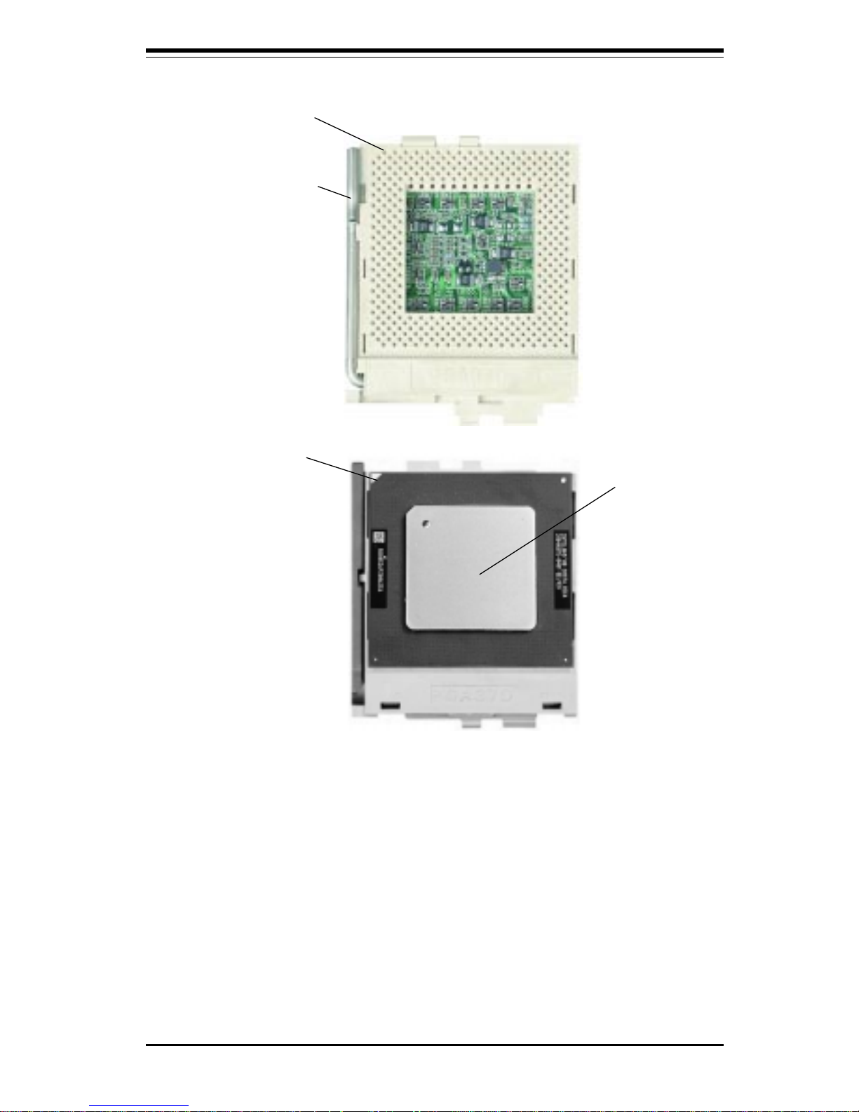
You are now ready to install the processor. Your motherboard has a 370pin, FCPGA type socket, which supports single or dual PentiumTM III FCPGA
500 MHz-1.4 GHz processors and low power single or dual PentiumTM III
processors at front bus speeds of 133 and 100 MHz. Lift the lever on the
FCPGA socket and install with the notched corner of the processor oriented
with pin 1. Fully seat the processor into the socket and then close the
lever.
Heat Sink
Follow the instructions that came with your processor or heat sink to
attach a heat sink to the processor. Your heat sink should have a 3-pin
fan, which connects to the CPU FAN header. Make sure that good
contact is made between the CPU chip and the heat sink. Insufficient
contact will cause the processor to overheat, which may crash the
system.
2-2 FCPGA Processor Installation
When handling the processor package, avoid placing
direct pressure on the label area of the fan.
The following pages cover the installation procedure. You should install the
processor in the motherboard first, then install the motherboard in the chassis, then the memory and add-on cards, and finally the cables and drivers.
Following the installation procedures in the order they appear in this chapter should eliminate the most common problems encountered when installing
a system.
IMPORTANT: Always connect the power cord last and always remove it before adding, removing or changing any hardware components.
!
Chapter 2: Installation
2-3
2-3 Mounting the Motherboard in the Chassis
All motherboards have standard mounting holes to fit different types of
chassis. Chassis may include a variety of mounting fasteners made of
metal or plastic. Although a chassis may have both types, metal fasteners
are the most highly recommended because they ground the motherboard to
the chassis. For this reason, it is best to use as many metal fasteners as
possible.
Figure 2-1. FCPGA Socket: Empty and with Processor Installed
Pin 1
Lever
Notched
Corner
Processor
(installed)
2-4
SUPER P3TDL3/P3TDLE User’s Manual
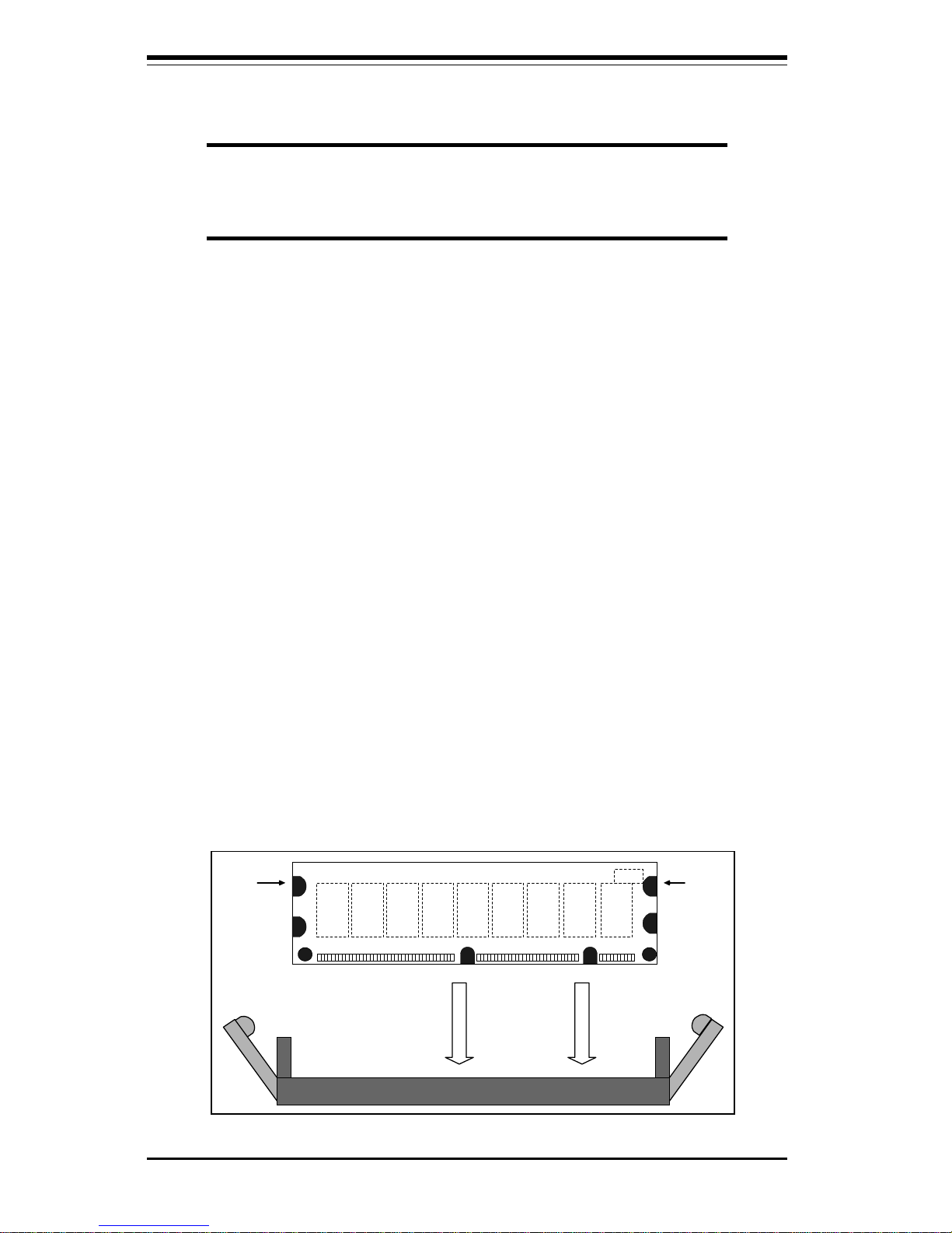
Figure 2-4. Side View of DIMM Installation into Slot
To Install: Insert module vertically and press down until it
snaps into place. Pay attention to the two notches.
No te: N otc h es
should align
w ith th e
rece p tive p o in ts
on the slot
DIMM Slot
DIMM
Notches Notches
2-4 Installing DIMMs
CAUTION
Exercise extreme care when installing or removing DIMM
modules to prevent any possible damage.
NOTE: Check the Supermicro web site for recommended memory
modules:
http://www.supermicro.com/TECHSUPPORT/FAQs/Memory_vendors.htm
DIMM Installation (See Figure 2-4)
1. Insert DIMMs as required for the desired system memory.
2. Insert each DIMM module vertically into its slot. Pay attention to the
two notches along the bottom of the module to prevent inserting the
DIMM module incorrectly.
3. Gently press down on the DIMM module until it snaps into place in the
slot.
4. Start DIMM insertion at the DIMM0 slot and continue numerically
through the DIMM3 slot, as needed.
Support
The P3TDL3/P3TDLE supports only registered ECC PC100 and PC133
SDRAM. Note that the memory and front side bus speeds are synchronized, meaning if PC133 is used with a 100 MHz FSB, the memory will
run at 100 MHz.
Chapter 2: Installation
2-5
Top View of DIMM Slot
Release Tab Release Tab
To Remove:
Use your thumbs to gently push each release tab outward.
This should release the DIMM from the slot.
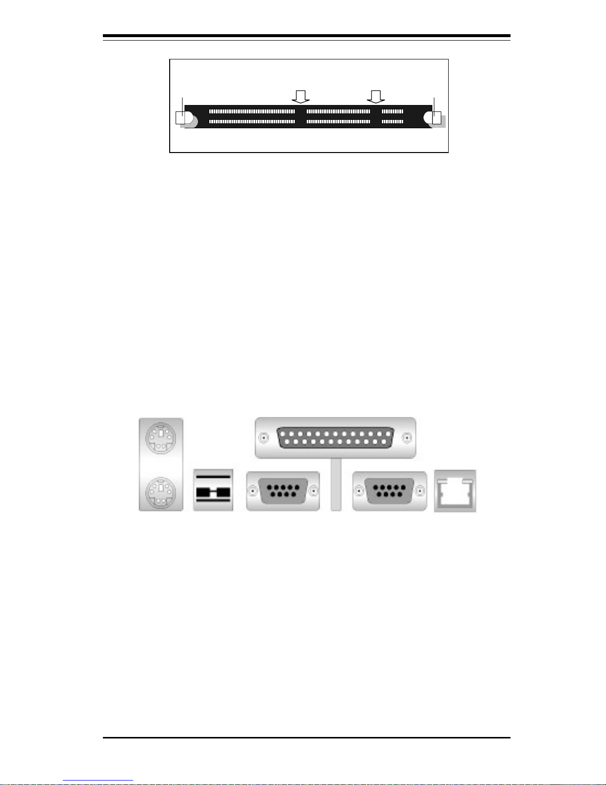
2-5 Port/Control Panel Connector Locations
The I/O ports are color coded in conformance with the PC 99 specification.
See Figure 2-5 below for the colors and locations of the various I/O ports.
Figure 2-5. I/O Port Locations and Definitions
Parallel Port
(Burgundy)
COM1 COM2Keyboard
(Purple)
Mouse
(Green)
Ethernet
Port
(Black)
(Turquoise)
USB
Ports
(Black)
 Loading...