


®
SUPER 370DE6
SUPER 370DER
SUPER 370DEI
USER’S MANUAL
Revision 2.0
SUPER

The information in this User’s Manual has been carefully reviewed and is believed to be
accurate. The vendor assumes no responsibility for any inaccuracies that may be contained
in this document, makes no commitment to update or to keep current the information in this
manual, or to notify any person or organization of the updates.
Please Note: For the most up-to-date version of this manual, please
see our web site at www.supermicro.com.
SUPERMICRO COMPUTER reserves the right to make changes to the product described in
this manual at any time and without notice. This product, including software, if any, and
documentation may not, in whole or in part, be copied, photocopied, reproduced, translated or
reduced to any medium or machine without prior written consent.
IN NO EVENT WILL SUPERMICRO COMPUTER BE LIABLE FOR DIRECT, INDIRECT,
SPECIAL, INCIDENTAL, OR CONSEQUENTIAL DAMAGES ARISING FROM THE USE OR
INABILITY TO USE THIS PRODUCT OR DOCUMENTATION, EVEN IF ADVISED OF THE
POSSIBILITY OF SUCH DAMAGES. IN PARTICULAR, THE VENDOR SHALL NOT HAVE
LIABILITY FOR ANY HARDWARE, SOFTWARE, OR DATA STORED OR USED WITH THE
PRODUCT, INCLUDING THE COSTS OF REPAIRING, REPLACING, INTEGRATING,
INSTALLING OR RECOVERING SUCH HARDWARE, SOFTWARE, OR DATA.
Any disputes arising between manufacturer and customer shall be governed by the laws of
Santa Clara County in the State of California, USA. The State of California, County of Santa
Clara shall be the exclusive venue for the resolution of any such disputes. Supermicro's total
liability for all claims will not exceed the price paid for the hardware product.
Unless you request and receive written permission from SUPER MICRO COMPUTER, you
may not copy any part of this document.
Information in this document is subject to change without notice. Other products and
companies referred to herein are trademarks or registered trademarks of their respective
companies or mark holders.
Copyright © 2000-2001 by SUPER MICRO COMPUTER INC.
All rights reserved.
Printed in the United States of America.
Preface

iii
Preface
PREFACE
About This Manual
This manual is written for system integrators, PC technicians and
knowledgeable PC users. It provides information for the installation and use
of the SUPER 370DE6/370DER(370DER+)/370DEI(370DEI+) mainboard. The
SUPER 370DE6/370DER/370DER+/370DEI/370DEI+ supports single or dual
Pentium® III 500 MHz-1.13 GHz FCPGA processors with a 133/100 MHz
front side bus. Please refer to the support section of our web site (http://
www.supermicro.com/TechSupport.htm) for a complete listing of supported
processors.
Pentium III FCPGA (Flip Chip Pin Grid Array) processors are housed in a
370-pin socket, which is the standard that will support future Intel processors. The 370DER/370DER+/370DEI/370DEI+ were designed specifically for
use in rackmount 1-U systems.
Manual Organization
Chapter 1 includes a checklist of what should be included in your
mainboard box, describes the features, specifications and performance of
the SUPER 370DE6/370DER/370DER+/370DEI/370DEI+ mainboard and provides detailed information about the chipset.
Chapter 2 begins with instructions on handling static-sensitive devices.
Read this chapter when you want to install the processor and DIMM memory
modules and when mounting the mainboard in the chassis. Also refer to
this chapter to connect the floppy and hard disk drives, SCSI drives, the IDE
interfaces, the parallel and serial ports and the twisted wires for the power
supply, the reset button, the power LED, the speaker and the keyboard.
If you encounter any problems, see Chapter 3, which describes troubleshooting procedures for the video, the memory and the setup configuration
stored in CMOS. For quick reference, a general FAQ [Frequently Asked
Questions] section is provided. Instructions are also included for contacting technical support. In addition, you can visit our web site at
www.supermicro.com/techsupport.htm for more detailed information.
Chapter 4 includes an introduction to BIOS and provides detailed information on running the CMOS Setup utility.
Appendix A gives information on BIOS error beep codes.
Appendix B provides post checkpoint codes.

iv
SUPER 370DE6/370DER/370DEI User’s Manual
Preface
About This Manual ...................................................................................................... iii
Manual Organization ................................................................................................... ii i
Chapter 1: Introduction
1-1 Overview ......................................................................................................... 1-1
Checklist .................................................................................................... 1-1
Contacting Supermicro ............................................................................ 1-2
Notes .......................................................................................................... 1-3
SUPER 370DE6 SECTION....................................................................... 1-4
SUPER 370DE6 Image ............................................................................. 1-5
SUPER 370DE6 Layout............................................................................ 1-6
SUPER 370DE6 Quick Reference.......................................................... 1-7
SUPER 370DER SECTION ...................................................................... 1-8
SUPER 370DER Image ............................................................................. 1-9
SUPER 370DER Layout ......................................................................... 1-10
SUPER 370DER+ Layout ....................................................................... 1-11
SUPER 370DER Quick Reference ....................................................... 1-1 2
SUPER 370DER+ Quick Reference ..................................................... 1-13
SUPER 370DEI SECTION...................................................................... 1-14
SUPER 370DEI Image ............................................................................. 1-15
SUPER 370DEI Layout ........................................................................... 1-16
SUPER 370DEI+ Layout......................................................................... 1-17
SUPER 370DEI Quick Reference ......................................................... 1-18
SUPER 370DEI+ Quick Reference ....................................................... 1-19
General SECTION ................................................................................. 1-20
Features of Motherboards .................................................................... 1-21
Server Works HE-SL Chipset: System Block Diagram..................... 1-23
1-2 Chipset Overview......................................................................................... 1-24
1-3 Special Features........................................................................................... 1-24
ATI Graphics Controller ........................................................................ 1-24
BIOS Recovery ....................................................................................... 1-2 4
Recovery from AC Power Loss ......................................................... 1-24
1-4 PC Health Monitoring.................................................................................... 1-25
1-5 ACPI/PC 98 Features ................................................................................... 1-26
1-6 Power Supply ............................................................................................... 1-28
1- 7 Super I/O ......................................................................................................... 1-28
Chapter 2: Installation
2-1 Static-Sensitive Devices ............................................................................... 2-1
Precautions............................................................................................... 2-1
Unpacking.................................................................................................. 2-1
2- 2 FCPGA Processor Installation ...................................................................... 2-2
2-3 Installing DIMMs............................................................................................... 2-4

Table of Contents
v
2- 4 Port/Control Panel Connector Locations ..................................................... 2-5
2-5 Connecting Cables .......................................................................................... 2-8
Power Supply Connector ....................................................................... 2-8
Power LED ................................................................................................. 2-8
Hard Drive LED ........................................................................................ 2-8
PWR_ON .................................................................................................... 2-9
NIC_LED ..................................................................................................... 2-9
Reset.......................................................................................................... 2-9
I2C ................................................................................................................ 2-9
Chassis Intrusion ................................................................................... 2-10
Keyboard Lock ....................................................................................... 2-10
Overheat LED ......................................................................................... 2-10
Extra Universal Serial Bus Connection (USB3) ................................ 2-10
Speaker ................................................................................................... 2-1 1
Fan Headers ........................................................................................... 2-11
Serial Ports ............................................................................................. 2-11
ATX PS/2 Keyboard and Mouse Ports ................................................2-11
Universal Serial Bus Connector .......................................................... 2-12
Extra Universal Serial Bus Connection (USB4) ................................ 2-12
Wake-On-LAN ......................................................................................... 2-12
Power Supply Fail Header ................................................................... 2-13
SLED1 (SCSI LED) Indicator................................................................. 2-13
2- 6 DIP Switch Settings ..................................................................................... 2-14
DIP Switch 1: Core/Bus Ratio .............................................................. 2-14
2- 7 Jumper Settings ............................................................................................ 2-14
CMOS Clear............................................................................................. 2-15
Front Side Bus Speed .......................................................................... 2-15
SCSI Termination Enable/Disable.......................................................... 2-16
Speaker Enable/Disable ......................................................................... 2-16
Onboard LAN/NIC Enable/Disable......................................................... 2-16
Third Power Supply Failure Alarm Enable/Disable ........................... 2-17
2- 8 Parallel Port, Floppy/Hard Disk Drive and SCSI Connections ............... 2-17
Parallel Port Connector ......................................................................... 2-17
Floppy Connector ................................................................................... 2-18
IDE Connectors ...................................................................................... 2-1 8
Ultra160 SCSI Connector....................................................................... 2-19
Installing Software Drivers .................................................................. 2-20
Table of Contents

SUPER 370DE6/370DER/370DEI User’s Manual
Chapter 3: Troubleshooting
3-1 Troubleshooting Procedures ........................................................................ 3-1
Before Power On .................................................................................... 3-1
No Power .................................................................................................. 3-1
No Video ................................................................................................... 3-1
Memory Errors .......................................................................................... 3-2
Losing the System’s Setup Configuration ........................................... 3-2
3-2 Technical Support Procedures .................................................................... 3-2
3-3 Frequently Asked Questions........................................................................ 3-3
3-4 Returning Merchandise for Service............................................................ 3-5
Chapter 4: BIOS
4-1 Introduction....................................................................................................... 4-1
4-2 BIOS Features ................................................................................................. 4-2
4-3 Running Setup ................................................................................................. 4-2
Standard CMOS Setup ............................................................................. 4-3
4-4 Advanced CMOS Setup .................................................................................. 4-4
4- 5 Chipset Setup................................................................................................. 4-15
4-6 PCI/Plug and Play Setup ............................................................................... 4-18
4-7 Power Setup .................................................................................................. 4-22
4- 8 Boot Setup...................................................................................................... 4-25
4-9 Security Setup ............................................................................................... 4-27
4-10 Exit Setup ....................................................................................................... 4-29
Appendices:
Appendix A: BIOS Error Beep Codes ....................................................................A-1
Appendix B: AMIBIOS Post Checkpoint Codes .................................................... B-1
vi

Notes
SUPER 370DE6/370DER/370DEI User’s Manual
viii

Chapter 1: Introduction
1-1
Introduction
Chapter 1
Introduction
1-1 Overview
Checklist
Congratulations on purchasing your computer motherboard from an acknowledged leader in the industry. Supermicro boards are designed with
the utmost attention to detail to provide you with the highest standards in
quality and performance.
Please check that the following items have all been included with your
motherboard. If anything listed here is damaged or missing, contact your
retailer.
One (1) Supermicro Mainboard
One (1) ribbon cable for IDE devices
One (1) floppy ribbon cable for (a) 5.25-inch floppy and
(b) 3.5-inch floppy drives
One (1) I/O backpanel shield
SCSI Accessories (not with 370DEI/370DEI+):
One (1) 50-pin Ultra SCSI cable (370DE6 only)
One (1) 68-pin LVD SCSI cable
One (1) set of SCSI driver diskettes
One (1) SCSI manual
One (1) Supermicro CD or diskettes containing drivers and utilities
One (1) User's/BIOS Manual

SUPER 370DE6/370DER/370DEI User's Manual
1-2
Introduction
CONTACTING SUPERMICRO
Headquarters
Address: Super Micro Computer, Inc.
980 Rock Avenue
San Jose, CA 95131 U.S.A.
Tel: +1 (408) 503-8000
Fax: +1 (408) 503-8008
E-mail: marketing@supermicro.com (General Information)
support@supermicro.com (Technical Support)
Web site: www.supermicro.com
European Office
Address: Super Micro Computer B.V.
Het Sterrenbeeld 28, 5215 ML,
's-Hertogenbosch, The Netherlands
Tel: +31 (0) 73-6400390
Fax: +31 (0) 73-6416525
E-mail: sales@supermicro.nl (General Information)
support@supermicro.nl (Technical Support)
rma@supermicro.nl (Customer Support)
Asia-Pacific
Address: 6th Floor, No. 755 Chung-cheng Road
Chung-Ho City, Taipei Hsien, Taiwan, R.O.C.
Tel: 886 (2) 8221-1690
Fax: 886 (2) 8221-2790
www : www.supermicro.com.tw
Email: support@supermicro.com.tw

Chapter 1: Introduction
1-3
Introduction
Notes

SUPER 370DE6/370DER/370DEI User's Manual
1-4
Introduction
SUPER 370DE6
SECTION
Chapter 1: Introduction
1-5
Introduction
SUPER 370DE6
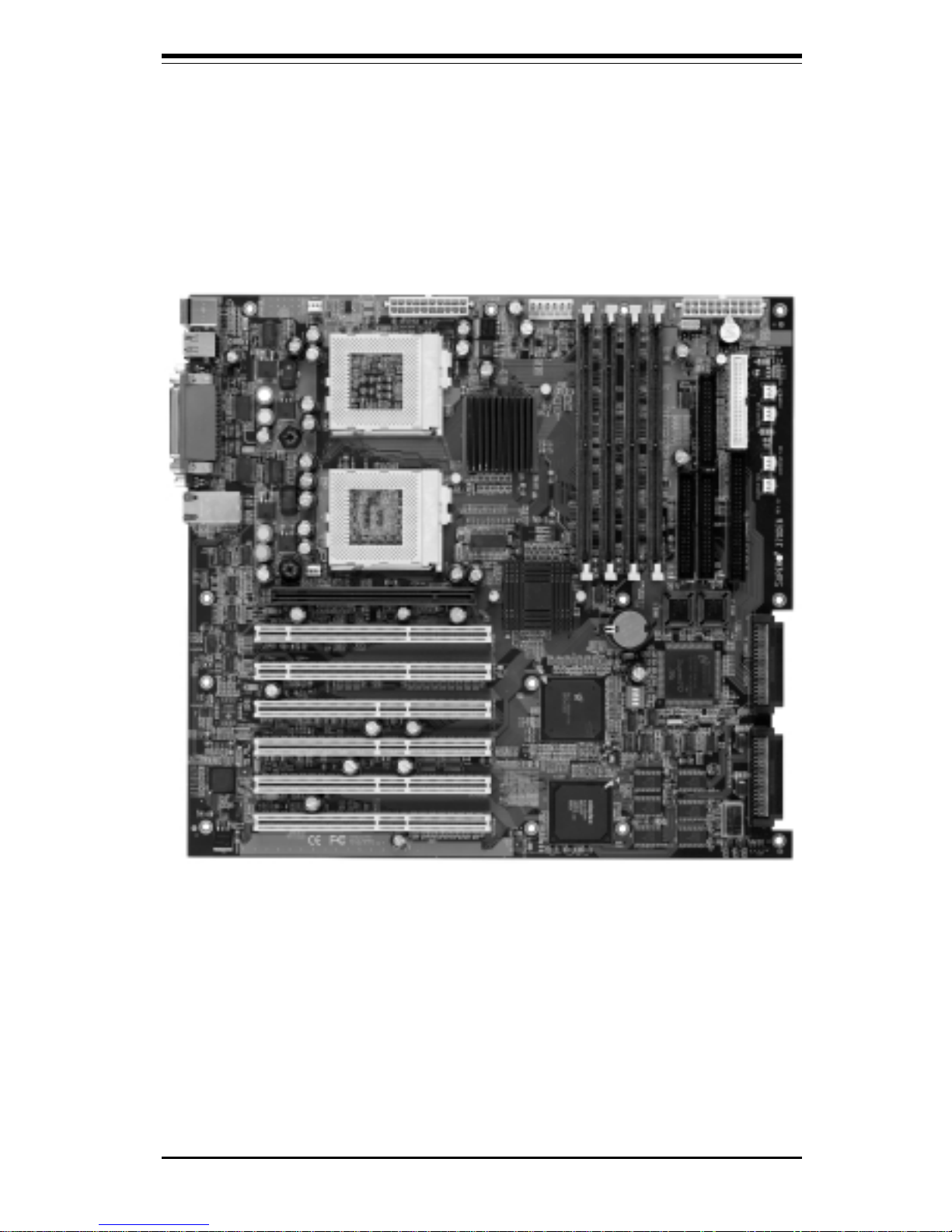
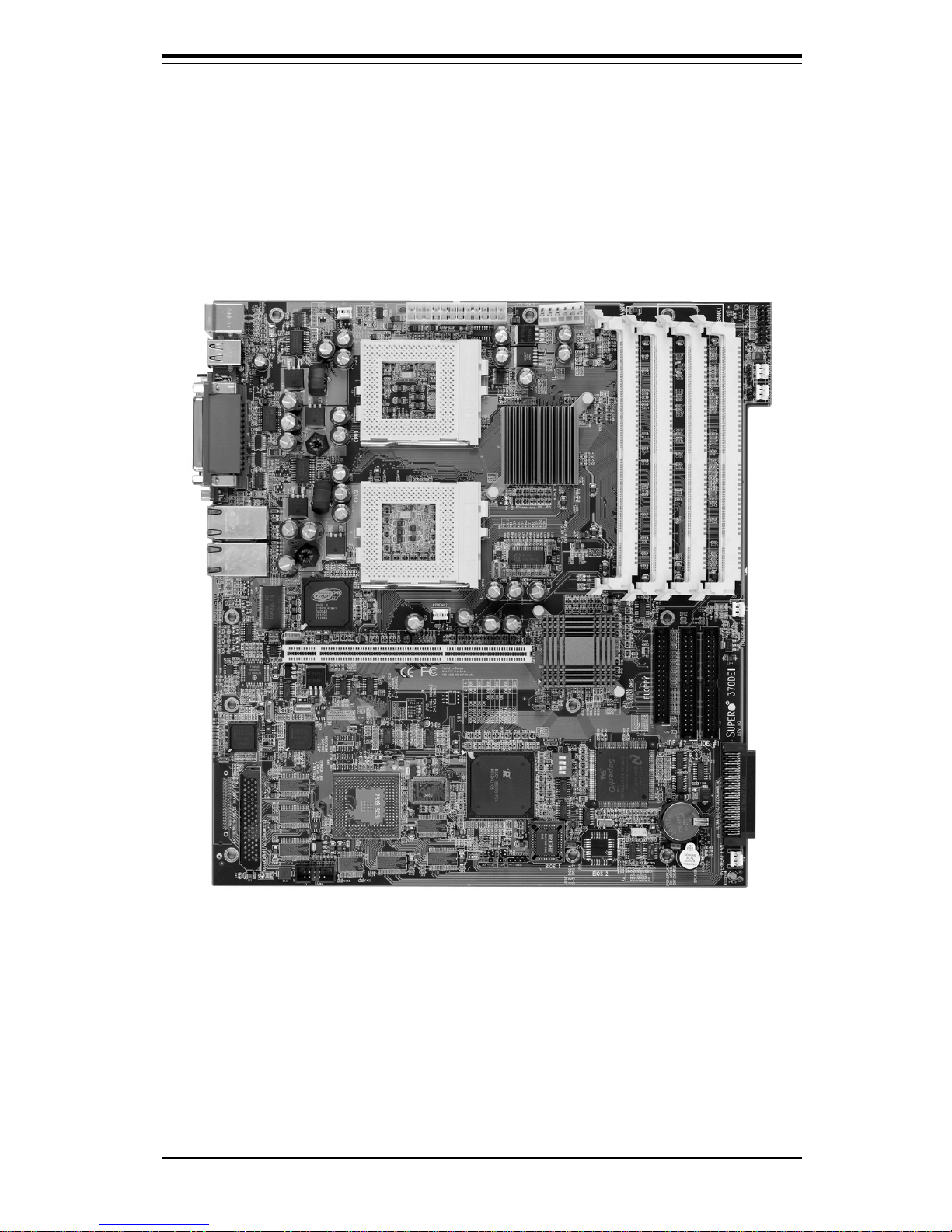
Figure 1-1. SUPER 370DE6 Image
SUPER 370DE6/370DER/370DEI User's Manual
1-6
Introduction
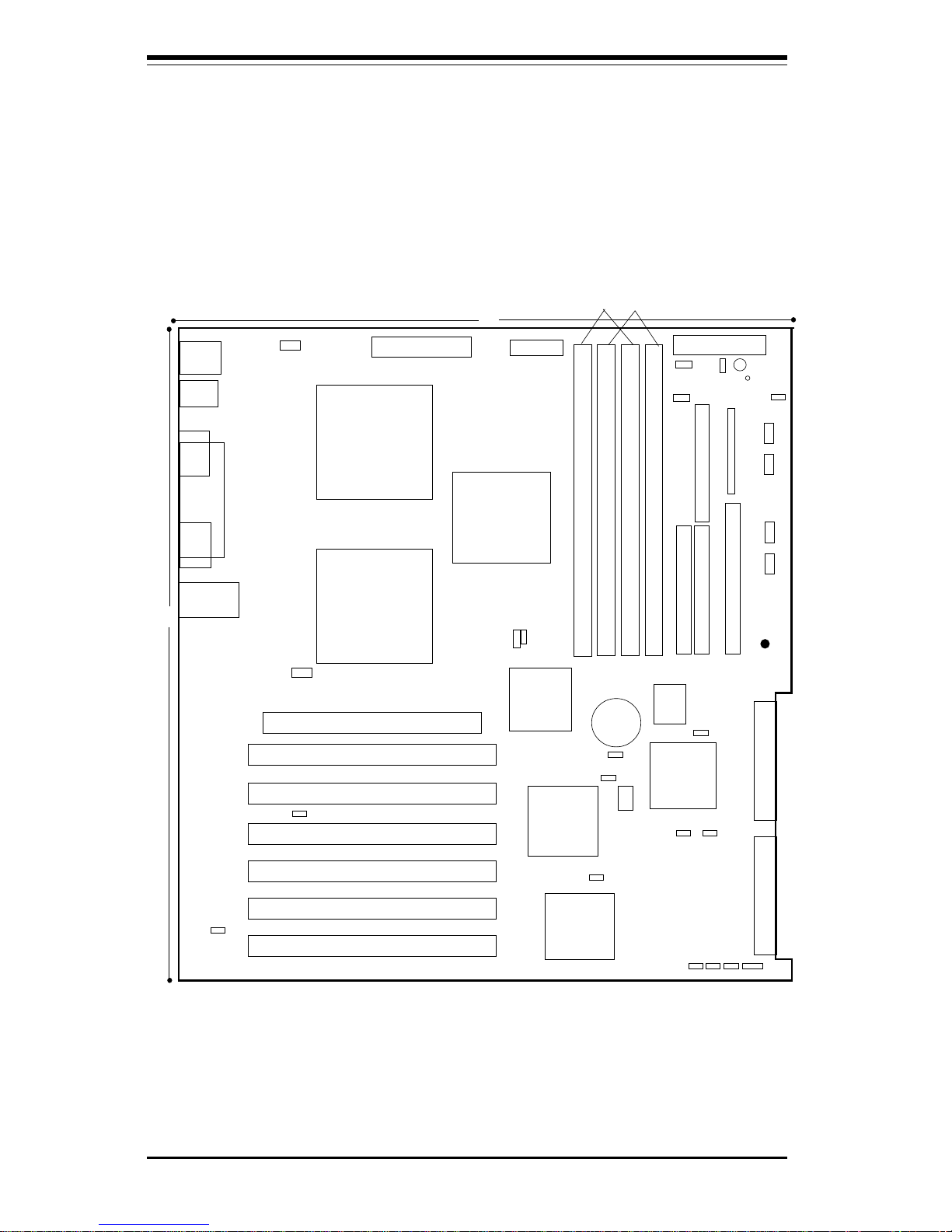
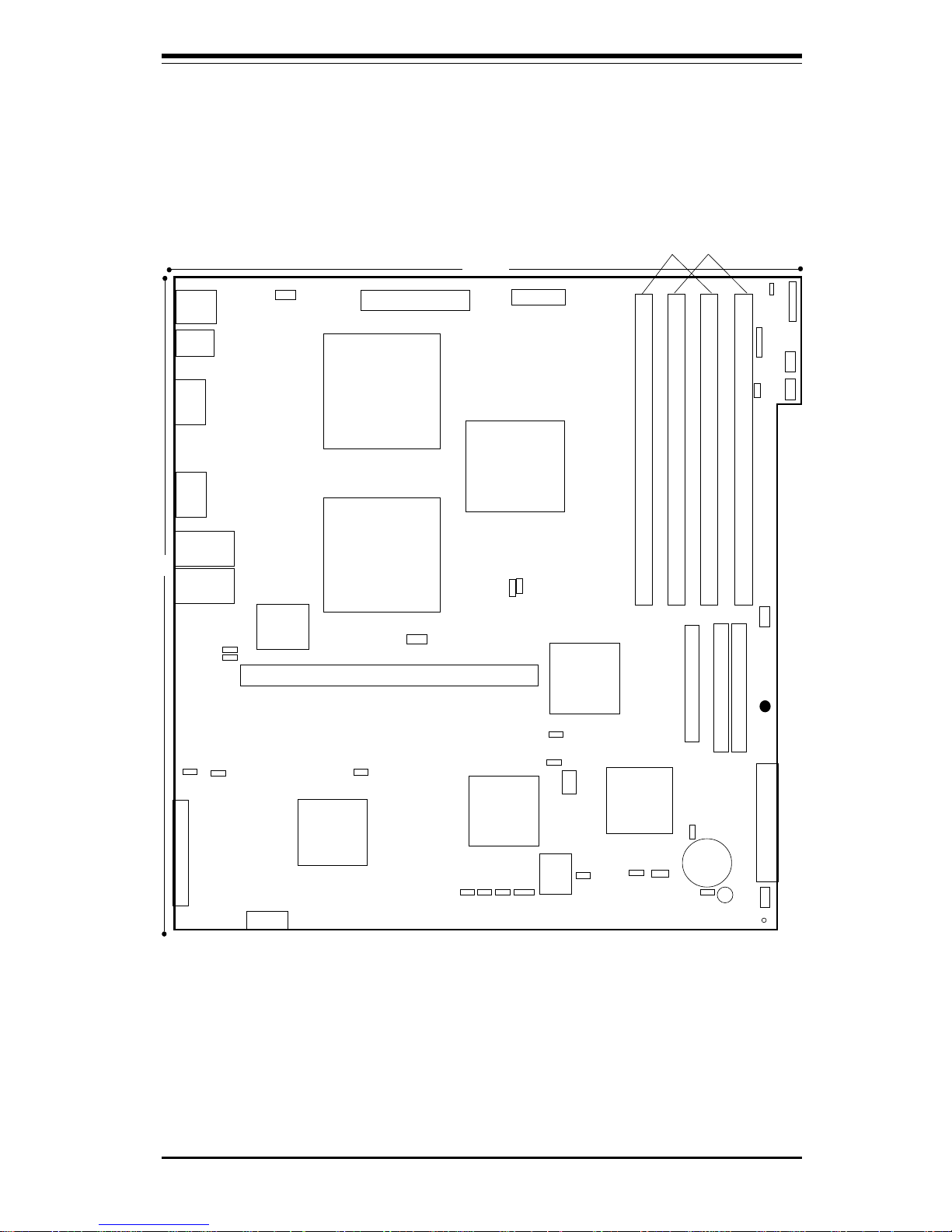
Figure 1-3. SUPER 370DE6 Layout
(not drawn to scale)
Also see the figure on page 2-5 for the locations of the I/O ports and
2-7 for the Front Control Panel (JF1) connectors.
SUPER 370DE6
USB
COM1
PS/2 KB/
MOUSE
B
A
T
T
E
R
Y
J16
Parallel
Port
FLO
PPY
13"
ATX POWER #1
CPU
FAN1
J18
®
CPU
1
CPU
FAN2
B
A
N
K
0
PWR_SEC
ID
E #1
ID
E #2
JP1
J13
J14
ULTRA160 LVD SCSI CHA
JF1
JP3
WOR
CPU
2
JP62
3V/PCI64#2
BIOS
SOUTH
BRIDGE
JP54
JP57
JA4
SLED
AIC-7899
SUPER
I/O
B
A
NK
1
B
A
N
K
0
B
A
N
K
1
OH FAN
CHASSIS FAN
SW1
NORTH
BRIDGE
JP58
COM2
LAN
J19
J15
POWER LED
JBT1
JA6 JA2
JP60
JP61
JP56
JA1
1
JP59
ATX POWER #2
OH FAN
CHASSIS FAN
U
ltra SC
S
I (C
hannel B
)
ULTRA160 LVD SCSI CHB
JA3
JA5
1
AGP PRO
3V/PCI64#1
5V/PCI64#4
5V/PCI64#3
5V/PCI64#2
5V/PCI64#1
1
JP55
Speaker
WOL
Bank0
Bank1
(*Notes: Memory modules should be installed in pairs only.)

Chapter 1: Introduction
1-7
Introduction
370DE6 Quick Reference
Jumpers Description Default Setting
JA2 LVD SCSI Ch A Term. Open (Enabled)
JA4 LVD SCSI Ch B Term. Open (Enabled)
JA6 50pin SCSI Ch B Term Open (Enabled)
JBT1 CMOS Clear Pin 1-2 (Normal)
JP1 FSB Speed Setting Pin 1-2 (Auto)
JP3 Spread Spectrum Enable Open (Disabled)
JP55 Third P/S Fail Enable/Disable Off (Disabled)
JP56 Speaker Enable/Disable On (Enabled)
JP57 BIOS Select Pin 1-2 (BIOS1)
JP58 LAN/NIC Enable/Disable Off (Enabled)
JP60 SCSI Enable/Disable Pin 1-2 (Enabled)
DIP Switch Description Default Setting
SW1(1-4) CPU Core/Bus Ratio
Connectors Description
ATX POWER #1 Primary ATX Power Connector
ATX POWER #2 Secondary ATX Power Connector BANK0BANK1 Memory (RAM) Slots
COM1/COM2 COM1/COM2 Serial Port Connector
CPU1/CPU2 CPU 1 and CPU2 Sockets
CPU/CH/OH FAN CPU/Overheat/Chassis Fan Headers
J13, J14 IDE Hard Disk Drive Connectors
J15 Floppy Disk Drive Connector
J16 Parallel Printer Port
J18 PS/2 Keyboard/Mouse
LAN Ethernet Port
JA1 Ultra160 LVD SCSI CH A Connector
JA3 Ultra160 LVD SCSI CH B Connector
JF1 Front Control Panel
JP54 Third Power Supply Fail Header
PWR_SEC Secondary ATX Power Connector
SLED1 SCSI Active LED header
USB Universal Serial Bus Ports
WOL Wake-on-LAN Header
WOR Wake-on-Ring Header
*Notes: Please refer to Chapter 2 for detailed information on
jumper settings and pin definitions.

SUPER 370DE6/370DER/370DEI User's Manual
1-8
Introduction
SUPER 370DER
SECTION
Chapter 1: Introduction
1-9
Introduction
SUPER 370DER
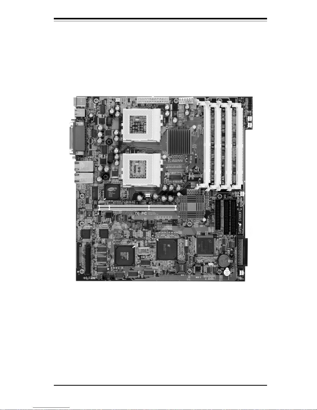
Figure 1-2. SUPER 370DER Image
SUPER 370DE6/370DER/370DEI User's Manual
1-10
Introduction
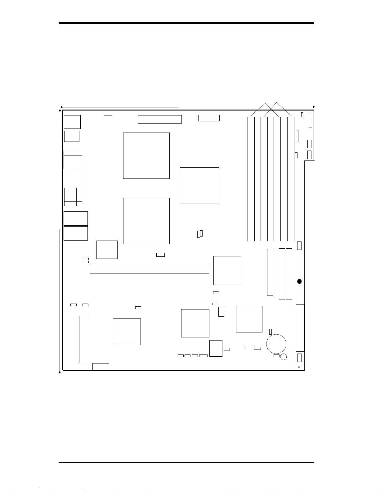
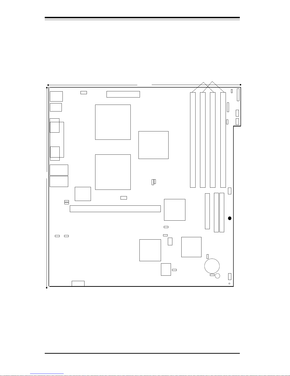
Figure 1-4. SUPER 370DER Layout
(not drawn to scale)
Also see the figure on page 2-6 for the locations of the I/O ports and
2-7 for the Front Control Panel (JF1) connectors.
(*Notes: Memory modules should be installed in pairs only.)
SUPER 370DER
USB
COM1
PS/2 KB/
MOUSE
B
A
T
T
E
R
Y
J16
Parallel
Port
FLO
P
PY
11.475"
ATX POWER
CPU
FAN1
J18
®
CPU
1
CPU
FAN2
CHASSIS FAN
B
A
N
K
0
PWR_SEC
ID
E #1
ID
E #2
JP1
J13 J14
ULTRA160 LVD SCSI CHA
JBT1
JF1
JP3
WOR
VGA
CPU
2
JP65
PWR LED
3V/PCI64
J11
BIOS
SOUTH
BRIDGE
WOL
JP56
JA4
1
SLED
1
AIC-7899
SUPER
I/O
B
AN
K
1
B
A
N
K
0
B
A
N
K
1
OH FAN
OVERHEAT FAN
CHASSIS FAN
SW1
NORTH
BRIDGE
COM2
Rage XL
VGA
LAN1
LAN2
J19
ULTRA160 LVD SCSI CHB
J15
POWER LED
SPEAKER
JP57
JA6 JA2
JP64
JP62
JP60
JP61
1
JP63
JA3
JA1
1
JP59
1
J214
Bank1Bank0
JP58
Chapter 1: Introduction
1-11
Introduction
Figure 1-4. SUPER 370DER+ Layout
(not drawn to scale)
(*Notes: Memory modules should be installed in pairs only.)
SUPER 370DER
USB
COM1
PS/2 KB/
MOUSE
B
A
T
T
E
R
Y
FLO
PPY
11.475"
ATX POWER
CPU
FAN1
J18
®
CPU
1
CPU
FAN2
CHASSIS FAN
BA
N
K
0
PWR_SEC
ID
E
#1
ID
E
#2
JP1
J13 J14
ULTRA160 LVD SCSI CHA
JBT1
JF1
JP3
WOR
VGA
CPU
2
JP65
PWR LED
3V/PCI64
J11
BIOS
SOUTH
BRIDGE
WOL
JP56
JA4
1
SLED
1
AIC-7899
SUPER
I/O
B
A
NK
1
BA
NK
0
B
A
N
K
1
OH FAN
OVERHEAT FAN
CHASSIS FAN
SW1
NORTH
BRIDGE
JP58
COM2
Rage XL
VGA
LAN1
LAN2
J19
J15
POWER LED
SPEAKER
JP57
JA6 JA2
JP64
JP60
JP61
1
JP63
JA1
1
JP59
1
J214
EXT ULTRA160 LVD SCSI CHB
JA5
Bank0
Bank1
JP62
Also see the figure on page 2-6 for the locations of the I/O ports and
2-7 for the Front Control Panel (JF1) connectors.

SUPER 370DE6/370DER/370DEI User's Manual
1-12
Introduction
370DER Quick Reference
Jumpers Description Default Setting
JA2 LVD SCSI Ch A Term. Open (Enabled)
JA4 LVD SCSI Ch B Term. Open (Enabled)
JA6 Manufacturer's Setting Always Closed
JBT1 CMOS Clear Pin 1-2 (Normal)
JP1 FSB Speed Setting Pin 1-2 (Auto)
JP3 Spread Spectrum Enable Closed (Disabled)
JP56 Speaker Enable/Disable On (Enabled)
JP57 BIOS Select Pin 1-2 (BIOS1)
JP58 LAN1 Enable/Disable Off (Enabled)
JP60 VGA Enable/Disable Pin 2-3 (Enabled)
JP61 VGA Interrupt Enable Pin 2-3 (Enabled)
JP62 LAN2 Enable/Disable Off (Enabled)
*JP63
(Notes) Chipset Speed Setting Off (133 MHz)
JP64 SCSI Enable/Disable Pin 1-2 (Enabled)
(*Note 1: for 370DER V.1.00 only.)
(*Note 2: If the FSB speed is 100MHz, JP63 should be set to "on".)
DIP Switches Description Default Setting
SW1(1-4) CPU Core/Bus Ratio
Connectors Description
ATX POWER Primary ATX Power Connector
BANK0/BANK1 Memory (RAM) Slots
COM1/COM2 COM1/2 Serial Port Conn/Header
CPU/CH/OH FAN CPU/Overheat/Chassis Fan Headers
J13, J14 IDE Hard Disk Drive Connectors
J15 Floppy Disk Drive Connector
J16 Parallel Printer Port
J18 PS/2 Keyboard/Mouse
J214 USB0 Header
JA1 Ultra160 Channel A LVD SCSI
JA3 Ultra160 Channel B LVD SCSI
JF1 Front Control Panel
LAN1/LAN2 Ethernet Port 1 / Ethernet Port 2
PWR_SEC Secondary ATX Power Connector
SLED1 SCSI Active LED header
USB Universal Serial Bus Ports
VGA Onboard VGA Monitor Connector
WOL Wake-on-LAN Header
WOR Wake-on-Ring Header
*Notes: Please refer to Chapter 2 for detailed information on
jumper settings and pin definitions.

Chapter 1: Introduction
1-13
Introduction
370DER+ Quick Reference
Jumpers Description Default Setting
JA2 LVD SCSI Ch A Term. Open (Enabled)
JA4 LVD SCSI Ch B Term. Open (Enabled)
JA6 Manufacturer's Setting Always Closed
JBT1 CMOS Clear Pin 1-2 (Normal)
JP1 FSB Speed Setting Pin 1-2 (Auto)
JP3 Spread Spectrum Enable Open (Disabled)
JP56 Speaker Enable/Disable On (Enabled)
JP57 BIOS Select Pin 1-2 (BIOS1)
JP58 LAN1 Enable/Disable Off (Enabled)
JP60 VGA Enable/Disable Pin 2-3 (Enabled)
JP61 VGA Interrupt Enable Pin 2-3 (Enabled)
JP62 LAN2 Enable/Disable Off (Enabled)
*JP63
(Notes) Chipset Speed Setting Off (133 MHz)
JP64 SCSI Enable/Disable Pin 1-2 (Enabled)
(*Note1 : 370DER+ V.1.00 only.)
(*Note2 : If the FSB speed is 100MHz, JP63 should be set to "On".)
DIP Switches Description Default Setting
SW1(1-4) CPU Core/Bus Ratio
Connectors Description
ATX POWER Primary ATX Power Connector
BANK0/BANK1 Memory (RAM) Slots
COM1/COM2 COM1/2 Serial Port Conn/Header
CPU/CH/OH FAN CPU/Overheat/Chassis Fan Headers
J13, J14 IDE Hard Disk Drive Connectors
J15 Floppy Disk Drive Connector
J18 PS/2 Keyboard/Mouse
J214 USB0 Header
JA1 Ultra160 Channel A LVD SCSI
JA5 External U160 Channel B LVD SCSI
JF1 Front Control Panel
LAN1/LAN2 Ethernet Port 1 / Ethernet Port 2
PWR_SEC Secondary ATX Power Connector
SLED1 SCSI Active LED header
USB Universal Serial Bus Ports
VGA Onboard VGA Monitor Connector
WOL Wake-on-LAN Header
WOR Wake-on-Ring Header
*Notes: Please refer to Chapter 2 for detailed information on
jumper settings and pin definitions.

SUPER 370DE6/370DER/370DEI User's Manual
1-14
Introduction
SUPER 370DEI
SECTION
Chapter 1: Introduction
1-15
Introduction
SUPER 370DEI
Figure 1-2. SUPER 370DEI Image
SUPER 370DE6/370DER/370DEI User's Manual
1-16
Introduction
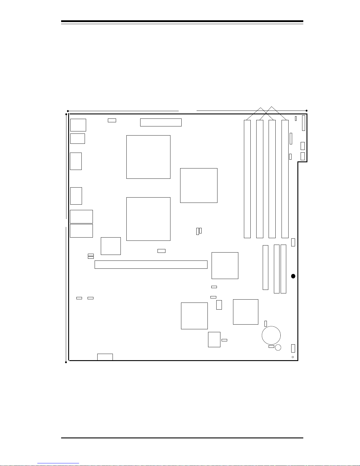
Figure 1-4. SUPER 370DEI Layout
(not drawn to scale)
(*Notes: Memory modules should be installed in pairs only.)
12.05"
SUPER 370DEI
USB
COM1
PS/2 KB/
MOUSE
B
A
T
T
E
R
Y
J16
Parallel
Port
FLO
P
PY
11.475"
ATX POWER
CPU
FAN1
J18
®
CPU
1
CPU
FAN2
CHASSIS FAN
B
A
N
K
0
ID
E #1
ID
E #2
JP1
J13 J14
JBT1
JF1
JP3
12.05"
VGA
CPU
2
JP65
PWR LED
3V/PCI64
J11
BIOS
SOUTH
BRIDGE
JP56
1
SUPER
I/O
BA
N
K
1
B
A
N
K
0
B
A
N
K
1
OH FAN
OVERHEAT FAN
CHASSIS FAN
SW1
NORTH
BRIDGE
COM2
Rage XL
VGA
LAN1
LAN2
J15
POWER LED
SPEAKER
JP57
JP62
JP60
JP61
1
JP63
1
JP59
1
J214
Bank1Bank0
JP58
Also see the figure on page 2-6 for the locations of the I/O ports and
2-7 for the Front Control Panel (JF1) connectors.
Chapter 1: Introduction
1-17
Introduction
12.05"
SUPER 370DEI
USB
COM1
PS/2 KB/
MOUSE
B
A
T
T
E
R
Y
FLO
PP
Y
11.475"
ATX POWER
CPU
FAN1
J18
®
CPU
1
CPU
FAN2
CHASSIS FAN
B
AN
K
0
ID
E
#1
ID
E
#2
JP1
J13 J14
JBT1
JF1
JP3
12.05"
VGA
CPU
2
JP65
PWR LED
3V/PCI64
J11
BIOS
SOUTH
BRIDGE
JP56
1
SUPER
I/O
B
A
N
K
1
B
A
N
K
0
B
A
N
K
1
OH FAN
OVERHEAT FAN
CHASSIS FAN
SW1
NORTH
BRIDGE
COM2
Rage XL
VGA
LAN1
LAN2
J15
POWER LED
SPEAKER
JP57
JP62
JP60
JP61
1
JP63
1
JP59
1
J214
Bank1Bank0
JP58
(*Notes: Memory modules should be installed in pairs only.)
Figure 1-4. SUPER 370DEI+ Layout
(not drawn to scale)
Also see the figure on page 2-6 for the locations of the I/O ports and
2-7 for the Front Control Panel (JF1) connectors.

SUPER 370DE6/370DER/370DEI User's Manual
1-18
Introduction
370DEI Quick Reference
Jumpers Description Default Setting
JBT1 CMOS Clear Pin 1-2 (Normal)
JP1 FSB Speed Setting Pin 1-2 (Auto)
JP3 Spread Spectrum Enable Open (Disabled)
JP56 Speaker Enable/Disable On (Enabled)
JP57 BIOS Select Pin 1-2 (BIOS1)
JP58 LAN1 Enable/Disable Off (Enabled)
JP60 VGA Enable/Disable Pin 2-3 (Enabled)
JP61 VGA Interrupt Enable Pin 2-3 (Enabled)
JP62 LAN2 Enable/Disable Off (Enabled)
*JP63 Chipset Speed Setting Off (133 MHz)
(*Note1 : If the FSB speed is 100MHz, JP63 should be set to "On".)
DIP Switches Description Default Setting
SW1(1-4) CPU Core/Bus Ratio
Connectors Description
ATX POWER Primary ATX Power Connector
BANK0/BANK1 Memory (RAM) Slots
COM1/COM2 COM1/2 Serial Port Conn/Header
CPU/CH/OH FAN CPU/Overheat/Chassis Fan Headers
J13, J14 IDE Hard Disk Drive Connectors
J15 Floppy Disk Drive Connector
J16 Parallel Printer Port
J18 PS/2 Keyboard/Mouse
J214 USB0 Header
JA1 Ultra160 Channel A LVD SCSI
JA5 External U160 Channel B LVD SCSI
JF1 Front Control Panel
LAN1/LAN2 Ethernet Port 1 / Ethernet Port 2
PWR_SEC Secondary ATX Power Connector
USB Universal Serial Bus Ports
VGA Onboard VGA Monitor Connector
WOL Wake on Lan
WOR Wake on Ring
*Notes: Please refer to Chapter 2 for detailed information on
jumper settings and pin definitions.

Chapter 1: Introduction
1-19
Introduction
370DEI+ Quick Reference
Jumpers Description Default Setting
JBT1 CMOS Clear Pin 1-2 (Normal)
JP1 FSB Speed Setting Pin 1-2 (Auto)
JP3 Spread Spectrum Enable Open (Disabled)
JP56 Speaker Enable/Disable On (Enabled)
JP57 BIOS Select Pin 1-2 (BIOS1)
JP58 LAN1 Enable/Disable Off (Enabled)
JP60 VGA Enable/Disable Pin 2-3 (Enabled)
JP61 VGA Interrupt Enable Pin 2-3 (Enabled)
JP62 LAN2 Enable/Disable Off (Enabled)
*JP63 Chipset Speed Setting Off (133 MHz)
(*Note1 : If the FSB speed is 100MHz, JP63 should be set to "On".)
DIP Switches Description Default Setting
SW1(1-4) CPU Core/Bus Ratio
Connectors Description
ATX POWER Primary ATX Power Connector
BANK0/BANK1 Memory (RAM) Slots
COM1/COM2 COM1/2 Serial Port Conn/Header
CPU/CH/OH FAN CPU/Overheat/Chassis Fan Headers
J13, J14 IDE Hard Disk Drive Connectors
J15 Floppy Disk Drive Connector
J18 PS/2 Keyboard/Mouse
J214 USB0 Header
JA1 Ultra160 Channel A LVD SCSI
JA5 External U160 Channel B LVD SCSI
JF1 Front Control Panel
LAN1/LAN2 Ethernet Port 1 / Ethernet Port 2
PWR_SEC Secondary ATX Power Connector
USB Universal Serial Bus Ports
VGA Onboard VGA Monitor Connector
WOL Wake on Lan
WOR Wake on Ring
*Notes: Please refer to Chapter 2 for detailed information on
jumper settings and pin definitions.

SUPER 370DE6/370DER/370DEI User's Manual
1-20
Introduction
GENERAL
SECTION
Chapter 1: Introduction
1-21
Introduction
Features of the 370DE6/370DER/370DER+/370DEI
CPU
• Single or dual Pentium III FCPGA 500 MHz-1.13 GHz processors at 133
or 100 MHz front side bus
Note: Please refer to the support section of our web site for a complete listing of supported
processors. (http://www.supermicro.com/TechSupport.htm)
Memory
• Four 168-pin DIMM sockets supporting up to 4 GB registered ECC
SDRAM
Note 1: The memory speed must match the front side bus speed being used. (Both
133 or 100 MHz.)
Note 2: The DIMM slots on the 370DER are set at a 25° angle to provide a low
vertical profile.
Note 3: Memory Modules should be installed in pairs (first in the two slots of Bank0,
then in both slots of Bank1, if needed).
Chipset
• ServerWorks ServerSet III HE Super Light (see page 1-13 for details)
Expansion Slots
370DE6: 370DER/DER+/DEI:
• Two 64-bit, 66/33 MHz PCI slots • One 64-bit, 66/33 MHz PCI
• Four 64-bit, 33 MHz PCI slots slot
• One 2x/AGP Pro slot
BIOS
• 4 Mb AMI® Flash ROM
• APM 1.2, DMI 2.1, PCI 2.2, ACPI 1.0, Plug and Play (PnP)
PC Health Monitoring
• Seven onboard voltage monitors for CPU core, chipset voltage, +5V
and +12V
• Fan status monitor with firmware/software on/off control
• Environmental temperature monitor and control
• CPU fan auto-off in sleep mode
• Power-up mode control for recovery from AC power loss
• System overheat LED and control
• System resource alert

SUPER 370DE6/370DER/370DEI User's Manual
1-22
Introduction
ACPI/PC 98 Features
• Microsoft OnNow
• Slow blinking LED for suspend state indicator
• Main switch override mechanism
• External modem ring-on
Onboard I/O
• AIC-7899 for dual channel Ultra160 SCSI (370DE6/370DER/370DER+)
• Integrated ATI Rage XL Graphics Controller (370DER/370DER+/370DEI)
• Intel 82559 for integrated onboard Ethernet (370DER/370DER+/370DEI)
• 2 EIDE bus master interfaces support Ultra DMA/33
• 1 floppy port interface (up to 2.88 MB)
• 2 Fast UART 16550A compatible serial ports
• 1 EPP/ECP (Enhanced Parallel Port/Extended Capabilities Port)
(370DE6/370DER/370DEI)
• PS/2 mouse and PS/2 keyboard ports
• 2 USB (Universal Serial Bus) ports
Other
• Internal/external modem ring-on
• Recovery from AC power loss control
• Wake-on-LAN (WOL)
CD/Diskette Utilities
• BIOS flash upgrade utility
• Device Drivers
Dimensions
• SUPER 370DE6
Extended ATX: 12.05" x 13" (306 x 330 mm)
• SUPER 370DER/370DER+/370DEI
Full ATX: 12.05" x 11.475" (306 x 291 mm)
Chapter 1: Introduction
1-23
Introduction
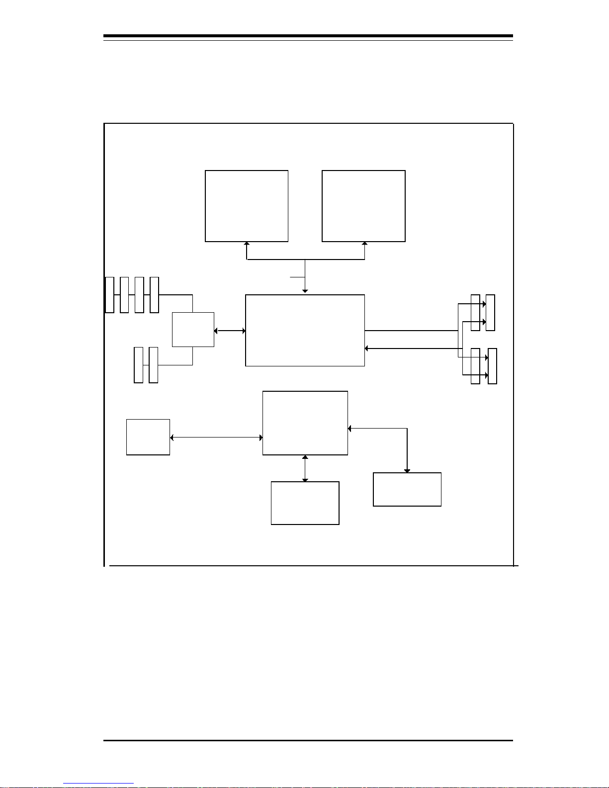
Figure 1-5. ServerWorks HE-SL Chipset:
System Block Diagram
*Note: This is a general block diagram. Please see the previous
Motherboard Features Section for details on the PCI slots included
on each motherboard.
CNB20HE-SL
Ho s t (N o rth ) B ridge
Pe n tiu m III
FCPGA
CPU*
OSB4
South Bridge
133/100 MHz Host Bus
PC133/PC100
Re
g
ist ered
DIMMs
USB
Ports
BIOS 4Mb
Flash ROM
1.5 Mb/sec
Pe n tiu m III
FCPGA
CPU*
ATA33 IDE
Ports
PCI 64/66
144-bit Data Bus
Address & Control
CIOB20
PCI 64/33
ECC
 Loading...