

Page 1

C9Z490-PG
C9Z490-PGW
USER'S MANUAL
Revision 1.0
Page 2

The information in this user’s manual has been carefully reviewed and is believed to be accurate. The manufacturer
!
assumes no responsibility for any inaccuracies that may be contained in this document, and makes no commitment
to update or to keep current the information in this manual, or to notify any person or organization of the updates.
Please Note: For the most up-to-date version of this manual, please see our website at www.supermicro.com.
Super Micro Computer, Inc. ("Supermicro") reserves the right to make changes to the product described in this manual
at any time and without notice. This product, including software and documentation, is the property of Supermicro and/
or its licensors, and is supplied only under a license. Any use or reproduction of this product is not allowed, except
as expressly permitted by the terms of said license.
IN NO EVENT WILL Super Micro Computer, Inc. BE LIABLE FOR DIRECT, INDIRECT, SPECIAL, INCIDENTAL,
SPECULATIVE OR CONSEQUENTIAL DAMAGES ARISING FROM THE USE OR INABILITY TO USE THIS PRODUCT
OR DOCUMENTATION, EVEN IF ADVISED OF THE POSSIBILITY OF SUCH DAMAGES. IN PARTICULAR, SUPER
MICRO COMPUTER, INC. SHALL NOT HAVE LIABILITY FOR ANY HARDWARE, SOFTWARE, OR DATA STORED
OR USED WITH THE PRODUCT, INCLUDING THE COSTS OF REPAIRING, REPLACING, INTEGRATING,
INSTALLING OR RECOVERING SUCH HARDWARE, SOFTWARE, OR DATA.
Any disputes arising between manufacturer and customer shall be governed by the laws of Santa Clara County in the
State of California, USA. The State of California, County of Santa Clara shall be the exclusive venue for the resolution
of any such disputes. Supermicro's total liability for all claims will not exceed the price paid for the hardware product.
FCC Statement: This equipment has been tested and found to comply with the limits for a Class B digital device
pursuant to Part 15 of the FCC Rules. These limits are designed to provide reasonable protection against harmful
interference when the equipment is operated in a consumer environment or residential installation. This equipment
generates, uses, and can radiate radio frequency energy and, if not installed and used in accordance with the
manufacturer’s instruction manual, may cause harmful interference with radio communications. Operation of this
equipment in a residential area is likely to cause harmful interference, in which case you will be required to correct
the interference at your own expense.
California Best Management Practices Regulations for Perchlorate Materials: This Perchlorate warning applies only
to products containing CR (Manganese Dioxide) Lithium coin cells. “Perchlorate Material-special handling may apply.
Refer to www.dtsc.ca.gov/hazardouswaste/perchlorate”.
WARNING: This product can expose you to chemicals including
lead, known to the State of California to cause cancer and birth
defects or other reproductive harm. For more information, go
to www.P65Warnings.ca.gov.
The products sold by Supermicro are not intended for and will not be used in life support systems, medical equipment,
nuclear facilities or systems, aircraft, aircraft devices, aircraft/emergency communication devices or other critical
systems whose failure to perform be reasonably expected to result in signicant injury or loss of life or catastrophic
property damage. Accordingly, Supermicro disclaims any and all liability, and should buyer use or sell such products
for use in such ultra-hazardous applications, it does so entirely at its own risk. Furthermore, buyer agrees to fully
indemnify, defend and hold Supermicro harmless for and against any and all claims, demands, actions, litigation, and
proceedings of any kind arising out of or related to such ultra-hazardous use or sale.
Manual Revision 1.0
Release Date: May 13, 2020
Unless you request and receive written permission from Super Micro Computer, Inc., you may not copy any part of this
document. Information in this document is subject to change without notice. Other products and companies referred
to herein are trademarks or registered trademarks of their respective companies or mark holders.
Copyright © 2020 by Super Micro Computer, Inc.
All rights reserved.
Printed in the United States of America
Page 3
Preface
Preface
About This Manual
This manual is written for system integrators, IT technicians and knowledgeable end users.
It provides information for the installation and use of the C9Z490-PG/-PGW motherboard.
About This Motherboard
The Supermicro C9Z490-PG/-PGW supports a single 10th Gen Intel® CoreTM i9/i7/i5/i3,
Pentium®, and Celeron® series (LGA1200) processor with up to 10 cores and a thermal
design power (TDP) of up to 125W. Built with the Intel PCH Z490 chipset, this motherboard
supports up to 128GB of Unbuered non-ECC UDIMM with speeds of up to 2933MHz (by
CPU) in four 288-pin memory slots, two M.2 sockets, 1G/10G Base-T ports, and a Trusted
Platform Module (TPM) header. The C9Z490-PG/-PGW is optimized for high-performance,
high-end computing platforms that address the needs of next generation server applications.
Please note that this motherboard is intended to be installed and serviced by professional
technicians only. For processor/memory updates, please refer to our website at http://www.
supermicro.com/products/.
Conventions Used in the Manual
Special attention should be given to the following symbols for proper installation and to prevent
damage done to the components or injury to yourself:
Warning! Indicates important information given to prevent equipment/property damage
or personal injury.
Warning! Indicates high voltage may be encountered while performing a procedure.
Important: Important information given to ensure proper system installation or to relay
safety precautions.
Note: Additional Information given to dierentiate various models or to provide information
for proper system setup.
3
Page 4

Super C9Z490-PG/-PGW User's Manual
Contacting Supermicro
Headquarters
Address: Super Micro Computer, Inc.
980 Rock Ave.
San Jose, CA 95131 U.S.A.
Tel: +1 (408) 503-8000
Fax: +1 (408) 503-8008
Email: marketing@supermicro.com (General Information)
support@supermicro.com (Technical Support)
Website: www.supermicro.com
Europe
Address: Super Micro Computer B.V.
Het Sterrenbeeld 28, 5215 ML
's-Hertogenbosch, The Netherlands
Tel: +31 (0) 73-6400390
Fax: +31 (0) 73-6416525
Email: sales@supermicro.nl (General Information)
support@supermicro.nl (Technical Support)
rma@supermicro.nl (Customer Support)
Website: www.supermicro.nl
Asia-Pacic
Address: Super Micro Computer, Inc.
3F, No. 150, Jian 1st Rd.
Zhonghe Dist., New Taipei City 235
Taiwan (R.O.C)
Tel: +886-(2) 8226-3990
Fax: +886-(2) 8226-3992
Email: support@supermicro.com.tw
Website: www.supermicro.com.tw
4
Page 5

Preface
Table of Contents
Chapter 1 Introduction
1.1 Checklist ...............................................................................................................................8
Quick Reference ...............................................................................................................12
Quick Reference Table ......................................................................................................13
Motherboard Features .......................................................................................................15
1.2 Processor and Chipset Overview .......................................................................................18
1.3 Special Features ................................................................................................................18
Recovery from AC Power Loss .........................................................................................18
1.4 System Health Monitoring ..................................................................................................19
Onboard Voltage Monitors ................................................................................................19
Fan Status Monitor with Firmware Control .......................................................................19
Environmental Temperature Control .................................................................................19
System Resource Alert......................................................................................................19
1.5 ACPI Features ....................................................................................................................20
Slow Blinking LED for Suspend-state Indicator ................................................................20
1.6 Power Supply ......................................................................................................................20
1.7 Serial Header .....................................................................................................................21
1.8 Super I/O ............................................................................................................................21
1.9 Intel Optane DC Persistent Memory Overview ..................................................................21
Chapter 2 Installation
2.1 Static-Sensitive Devices .....................................................................................................22
Precautions .......................................................................................................................22
Unpacking .........................................................................................................................22
2.2 Processor and Heatsink Installation ...................................................................................23
Installing the LGA1200 Processor ...................................................................................23
Installing an Active CPU Heatsink with Fan .....................................................................26
Removing an Active CPU Heatsink with Fan ...................................................................27
2.3 Motherboard Installation .....................................................................................................28
Tools Needed ....................................................................................................................28
Location of Mounting Holes ..............................................................................................28
Installing the Motherboard.................................................................................................29
5
Page 6

Super C9Z490-PG/-PGW User's Manual
2.4 Memory Support and Installation .......................................................................................30
General Guidelines for Optimizing Memory Performance ................................................30
DIMM Installation ..............................................................................................................31
DIMM Removal .................................................................................................................31
2.5 M.2 Installation (optional) ...................................................................................................32
2.6 Rear I/O Ports ...................................................................................................................34
2.7 Front Control Panel ............................................................................................................38
2.8 Connectors .........................................................................................................................42
Power Connections ...........................................................................................................42
Headers .............................................................................................................................44
2.9 Jumper Settings .................................................................................................................51
How Jumpers Work ...........................................................................................................51
2.10 LED Indicators ...................................................................................................................55
Chapter 3 Troubleshooting
3.1 Troubleshooting Procedures ..............................................................................................58
Before Power On ..............................................................................................................58
No Power ..........................................................................................................................58
No Video ...........................................................................................................................59
System Boot Failure .......................................................................................................59
Memory Errors ..................................................................................................................59
Losing the System's Setup Conguration .........................................................................60
When the System Becomes Unstable ..............................................................................60
3.2 Technical Support Procedures ...........................................................................................61
3.3 Frequently Asked Questions ..............................................................................................62
3.4 Battery Removal and Installation .......................................................................................63
Battery Removal ................................................................................................................63
Proper Battery Disposal ....................................................................................................63
Battery Installation .............................................................................................................63
3.5 Returning Merchandise for Service ....................................................................................64
6
Page 7

Preface
Chapter 4 UEFI BIOS
4.1 Introduction .........................................................................................................................65
4.2 EZ Mode .............................................................................................................................67
4.3 Main ....................................................................................................................................68
4.4 Overclocking .......................................................................................................................70
4.5 Advanced ............................................................................................................................92
4.6 H/W Monitor .....................................................................................................................125
4.7 Boot ..................................................................................................................................127
4.8 Save & Exit .......................................................................................................................129
4.9 BIOS Update ....................................................................................................................131
Appendix A BIOS Codes
A.1 BIOS Error POST (Beep) Codes .....................................................................................132
A.2 Additional BIOS POST Codes ..........................................................................................133
Appendix B Software
B.1 Driver Installation ..............................................................................................................134
B.2 SuperDoctor® 5 .................................................................................................................135
Appendix C Standardized Warning Statements
Appendix D UEFI BIOS Recovery
D.1 Overview ...........................................................................................................................139
D.2 Recovering the UEFI BIOS Image ...................................................................................139
D.3 Recovering the Main BIOS Block with a USB Device .....................................................139
7
Page 8
Super C9Z490-PG/-PGW User's Manual
Chapter 1
Introduction
Congratulations on purchasing your computer motherboard from an industry leader.
Supermicro motherboards are designed to provide you with the highest standards in quality
and performance.
In addition to the motherboard, several important parts that are included in the retail box are
listed below. If anything listed is damaged or missing, please contact your retailer.
1.1 Checklist
Main Parts List
Description Part Number Quantity
Supermicro Motherboard C9Z490-PG/-PGW 1
I/O Shield MCP-260-00147-0N 1
SATA Cables
Quick Reference Guide MNL-2238-QRG 1
Antenna (For C9Z490-PGW only) 2
S-Connector* JMP-0010L-0000-PRX 1
Note: The S-Connector is a plug designed to connect the front control panel header
on the motherboard and front control panel cables of chassis.
CBL-SAST-1000-2 2
CBL-SAST-1001-2 (Right-Angle SATA Cable) 2
Important Links
For your system to work properly, please follow the links below to download all necessary
drivers/utilities and the user’s manual for your server.
• Supermicro product manuals: http://www.supermicro.com/support/manuals/
• Product drivers and utilities: https://www.supermicro.com/wftp/driver
• Product safety info: https://www.supermicro.com/en/about/policies/safety-information
• A secure data deletion tool designed to fully erase all data from storage devices can be
found at our website: https://www.supermicro.com/about/policies/disclaimer.cfm?url=/
wftp/utility/Lot9_Secure_Data_Deletion_Utility/
• If you have any questions, please contact our support team at: support@supermicro.com
This manual may be periodically updated without notice. Please check the Supermicro website
for possible updates to the manual revision level.
8
Page 9
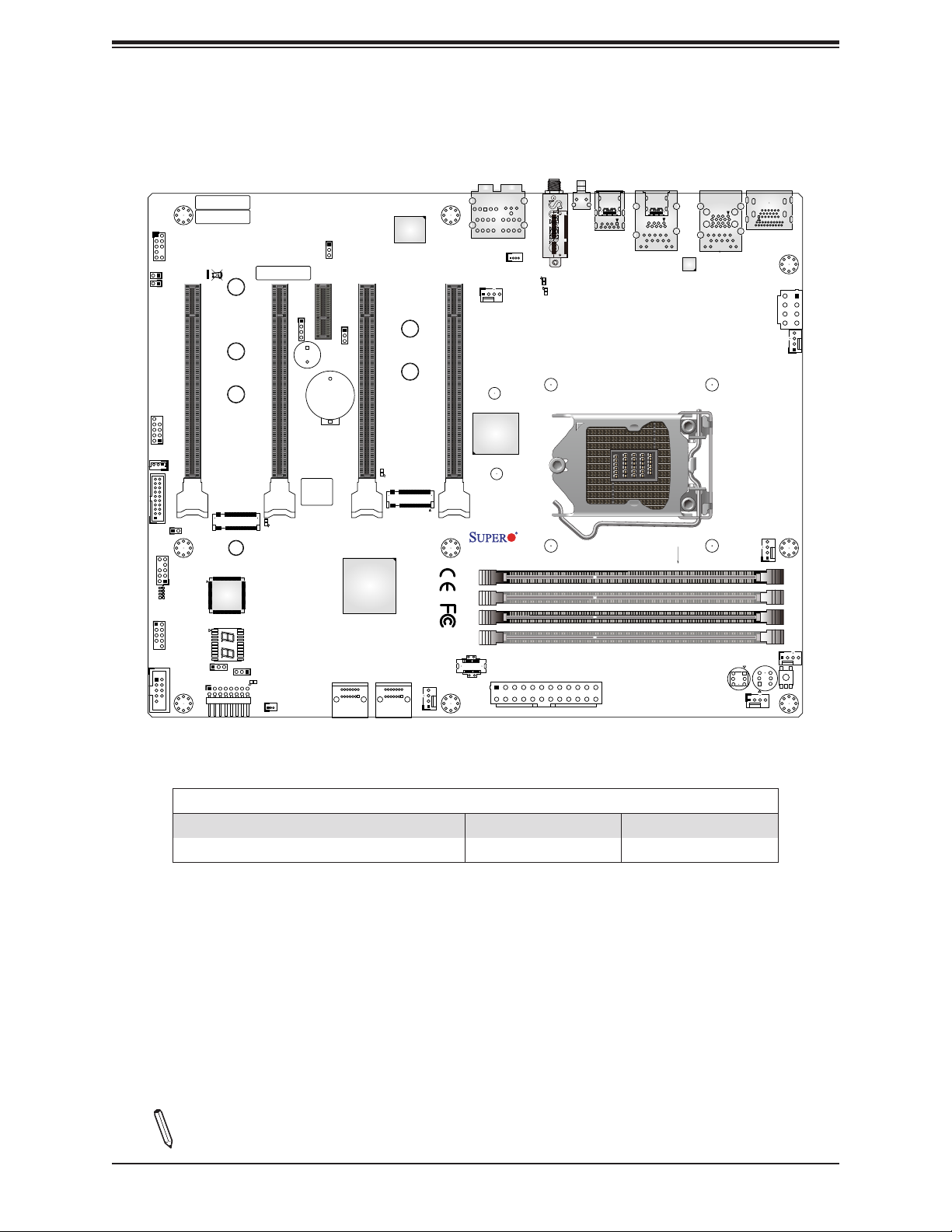
Figure 1-1. C9Z490-PGW Motherboard Image
Chapter 1: Introduction
Dierences between C9Z490-PG and C9Z490-PGW
C9Z490-PG C9Z490-PGW
PCI-E M.2 E Key for WiFi and Bluetooth No Yes
Note: All graphics shown in this manual were based upon the latest PCB revision available at the time of publication of the manual. The motherboard you received may or
may not look exactly the same as the graphics shown in this manual.
9
Page 10
Super C9Z490-PG/-PGW User's Manual
AUDIO FP
JI2C2
JI2C1
JSTBY1
JTPM1
USB2/3 (2.0)
USB0/1 (2.0)
USB10/11 (3.0)
CPU LED
DIMM LED
VGA LED
BOOT LED
COM1
JL1
MAC CODE
MAC CODE
MH10
CPU SLOT1 PCI-E 3.0 X8 (IN X16)
MH11
MH12
PCIE M.2-M1
MH14
Super I/O
LED4
JLED1
JWD1
JF1
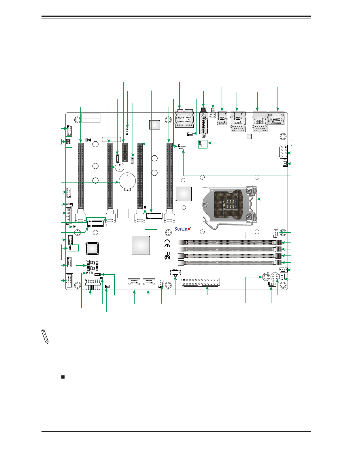
Figure 1-2. C9Z490-PG Motherboard Layout
(not drawn to scale)
10G LAN
Controller
MH15
CPU SLOT5 PCI-E 3.0 X8 (IN X 16)
MH13
LED2
PCIE M.2-M2
PCH
I-SATA0
I-SATA1
SYS_FAN2
SYS_FAN3
CPU SLOT7 PCI-E 3.0 X16
C9Z490-PG
REV:1.01
DESIGNED IN USA
USB12 (3.1)
HD AUDIO
JRLED1
PLX
JPW1
BAR CODE
CPU SLOT3 PCI-E 3.0 X16
JD1
LED3
LED1
JSD1
+
BIOS
LICENSE
JPAC1
PCH SLOT4 PCI-E 3.0 X1
1
JPME2
3
SP1
+
B1
I-SATA2
I-SATA3
SW1
(CLEAR CMOS)
USB8 (3.2)
USB9 (3.1)
LAN2 (1G)
USB6/7 (3.1) USB4/5 (3.0)
LAN Controller
DIMMA1
DIMMA2
DIMMB1
DIMMB2
LAN1 (10G)
POWER
BUTTON
DP/HDMI
JPW2
12V_PUMP_PWR1
RESET
BUTTON
CLEAR CMOS
SYS_FAN1
CPU_FAN2
CPU_FAN1
Note: Components not documented are for internal testing only.
10
Page 11
Chapter 1: Introduction
SYS_FAN2
AUDIO FP
JI2C2
JI2C1
JSTBY1
JTPM1
USB0/1
USB10/11 (3.2(5Gb))
CPU LED
DIMM LED
VGA LED
BOOT LED
JL1
MAC CODE
MAC CODE
MH10
CPU SLOT1 PCI-E 3.0 X8 (IN X16)
MH11
MH12
PCIE M.2-M1
MH14
Super I/O
Figure 1-2. C9Z490-PGW Motherboard Layout
(not drawn to scale)
SW1
(CLEAR CMOS)
PCIE M.2-E1
10G LAN
BAR CODE
CPU SLOT3 PCI-E 3.0 X16
JD1
LICENSE
LED3
+
BIOS
JPAC1
PCH SLOT4 PCI-E 3.0 X1
1
JPME2
3
SP1
+
B1
Controller
MH15
CPU SLOT5 PCI-E 3.0 X8 (IN X 16)
MH13
LED2
PCIE M.2-M2
PCH
SYS_FAN3
CPU SLOT7 PCI-E 3.0 X16
C9Z490-PGW
REV:1.01
DESIGNED IN USA
HD AUDIO
JRLED1
PLX
WiFi+BT
LED18
LED17
USB8 (3.2(10Gb))
USB9 (3.2(20Gb))
LAN2
USB6/7 (3.2(10Gb)) USB4/5 (3.2(5Gb))
LAN Controller
DIMMA1
DIMMA2
DIMMB1
DIMMB2
LAN1
DP/HDMI
JPW2
CPU_FAN2
12V_PUMP_PWR1
USB2/3
COM1
LED4
JLED1
LED1
JWD1
JF1
JSD1
I-SATA2
I-SATA3
I-SATA0
I-SATA1
USB12 (3.2(10Gb))
JPW1
Dierences between C9Z490-PG and C9Z490-PGW
C9Z490-PG C9Z490-PGW
PCI-E M.2 E Key for WiFi and Bluetooth No Yes
POWER
BUTTON
RESET
BUTTON
SYS_FAN1
CPU_FAN1
CLEAR CMOS
Note: Components not documented are for internal testing only.
11
Page 12
Super C9Z490-PG/-PGW User's Manual
PCH
PLX
Super I/O
LAN Controller
SW1
(CLEAR CMOS)
10G LAN
Controller
+
+
3
1
DESIGNED IN USA
C9Z490-PGW
REV:1.01
BIOS
LICENSE
MAC CODE
MAC CODE
BAR CODE
MH14
JRLED1
MH11
MH10
MH12
MH13
MH15
JSTBY1
JTPM1
HD AUDIO
B1
SP1
JD1
JSD1
SYS_FAN3
USB10/11 (3.2(5Gb))
JPW1
LED18
LED17
LED3
LED2
LED1
JPW2
JI2C2
JI2C1
JL1
LED4
JPAC1
JLED1
JWD1
JPME2
12V_PUMP_PWR1
USB9 (3.2(20Gb))
USB8 (3.2(10Gb))
USB2/3
JF1
BOOT LED
VGA LED
DIMM LED
CPU LED
DP/HDMI
LAN1
AUDIO FP
COM1
USB0/1
PCIE M.2-M1
CPU SLOT1 PCI-E 3.0 X8 (IN X16)
CPU SLOT3 PCI-E 3.0 X16
PCH SLOT4 PCI-E 3.0 X1
CPU SLOT5 PCI-E 3.0 X8 (IN X 16)
I-SATA1
I-SATA0
I-SATA3
I-SATA2
CPU SLOT7 PCI-E 3.0 X16
SYS_FAN2
PCIE M.2-M2
USB12 (3.2(10Gb))
USB6/7 (3.2(10Gb)) USB4/5 (3.2(5Gb))
POWER
BUTTON
DIMMB1
DIMMB2
DIMMA1
DIMMA2
RESET
BUTTON
SYS_FAN1
CPU_FAN1
CLEAR CMOS
CPU_FAN2
LAN2
PCIE M.2-E1
WiFi+BT
Quick Reference
DIMM LED
BOOT LED
AUDIO
FP
JI2C2
JI2C1
SP1
B1
USB0/1
JSTBY1
USB
10/11
LED3
JL1
PCIE-
M.2-M1
JTPM1
CPU LED
VGA LED
USB2/3
COM1
Notes:
Slot 4 Slot 5
JPAC1
JD1
Slot 1 Slot 3 Slot 7
JLED1
JWD1JF1LED4
LED1
JSD1
JPME2
I-SATA2
I-SATA3
HD AUDIO
PCIE M.2-M1
SYS_FAN3 JRLED1
I-SATA0
I-SATA1
SYS_FAN2
LED2
USB12
WiFi+BT
SW1
JPW1
USB8
USB9
LAN2
USB6
USB7
POWER
BUTTON
LAN1
USB4
USB5
SYS_FAN1
DP
HDMI
LED18
LED17
JPW2
CPU_
FAN2
SYS_
FAN1
CPU
12V_
PUMP_
PWR1
DIMMA1
DIMMA2
DIMMB1
DIMMB2
CPU_
FAN1
CLEAR
CMOS
RESET BUTTON
• Refer to Chapter 2 for detailed information on jumpers, I/O ports, and JF1 front panel
connections.
• " " indicates the location of Pin 1.
• Jumpers/LED indicators not indicated are used for testing only.
• Use only the correct type of onboard CMOS battery as specied by the manufacturer. Do
not install the onboard battery upside down to avoid possible explosion.
12
Page 13

Chapter 1: Introduction
Quick Reference Table
Jumper Description Default Setting
CLEAR CMOS Clear CMOS Switch Push Button Switch
JI2C1/JI2C2 SMB to PCI-E Slots Open (O): Disable
JPAC1 Audio Enable/Disable Pins 1-2 (Enable)
JPME2 Intel Manufacturing Mode Pins 1-2 (Normal)
JWD1 Watch Dog Function Enable Pins 1-2 (RST)
POWER BUTTON Internal Power Button Push Button Switch
RESET BUTTON Onboard System Reset Button Push Button Switch
SW1 Back Panel Clear CMOS Switch Push Button Switch
LED Description Color/State
BOOT LED Bootable Device POST (Power-On Self-Test) Status
CPU LED CPU POST (Power-On Self-Test) Status
DIMM LED DIMM POST (Power-On Self-Test) Status
LED1
LED17 WLAN POST (Power-On Self-Test) Status
LED18 Bluetooth Device POST (Power-On Self-Test) Status
LED2 PCI-E M.2-M2 Socket LED
LED3 PCI-E M.2-M1 Socket LED
LED4 BIOS POST Code LED Digital Readout
VGA LED Onboard VGA POST (Power-On Self-Test) Status
Onboard Power LED
S3 (Suspend to RAM) LED
Bootable Device POST: Orange ON
Bootable Device POST Completion: OFF
CPU POST: Yellow ON
CPU POST Completion: OFF
DIMM POST: Blue ON
DIMM POST Completion: OFF
Power On: Green On
S3: Green Blinking
WLAN POST: Green ON
WLAN POST Completion: OFF
Bluetooth Device POST: Green ON
Bluetooth Device POST Completion: OFF
PCI-E Device Detected: Green ON
Activity: Green Blinking
PCI-E Device Detected: Green ON
Activity: Green Blinking
Onboard VGA POST: Green ON
Onboard VGA POST Completion: OFF
Note: The table above is continued on the next page.
13
Page 14

Super C9Z490-PG/-PGW User's Manual
Connector Description
12V_PUMP_PWR1 12V 4-pin Power Connector for CPU Liquid Cooling Pump
AUDIO FP Front Panel Audio Header
B1 Onboard Battery
COM1 COM1 Header
CPU_FAN1 ~ CPU_FAN2 CPU Fan Headers
DP Back Panel DisplayPort
HD AUDIO High Denition Audio Ports
HDMI Back Panel High Denition Multimedia Interface
I-SATA0~3 (Intel Z490) Serial ATA (SATA 3.0) Ports 0~3 (6Gb/sec)
JD1 Speaker/Buzzer (Pins 1~4: External Speaker, Pins 3~4: Buzzer)
JF1 Front Control Panel Header
JL1 Chassis Intrusion Header
JLED1 Power LED Indicator Header
JPW1 24-pin ATX Main Power Connector (Required)
JPW2 +12V 8-pin CPU Power Connector (Required)
JRLED1 4-pin Connector for a White Light LED Board (Pre-installed) Inside the I/O cover
JSD1 SATA DOM (Disk-On-Module) Power Connector
JSTBY1 Standby Power Header
JTPM1 Trusted Platform Module (TPM)/Port 80 Header
LAN1/LAN2 RJ45 1GbE/10GbE LAN Ports
PCIE M .2- E1 M.2 E Key Socket for WiFi Module (Pre-installed, for C9Z490-PGW only)
PCIE M.2-M1/M.2-M2
SLOT1/5 PCI-E x16 Slots (PCI-E 3.0 x8 link)
SLOT3/7 PCI-E x16 Slots (PCI-E 3.0 x16 link)
SLOT4 PCI-E x1 Slot (PCI-E 3.0 x1 link)
SP1 Internal Speaker/Buzzer
SYS_FAN1 ~ SYS_FAN3 System Fan Headers
USB 0/1, 2/3 Front Panel Accessible USB 2.0 Headers
USB 4/5 Back Panel USB 3.2 Gen 1 Ports (Type A)
USB 6 Back Panel USB 3.2 Gen 2 Por t (Type A)
USB 7 Back Panel USB 3.2 Gen 2 Por t (Type C)
USB 8 Back Panel USB 3.2 Gen 2 Por t (Type A)
USB 9 Back Panel USB 3.2 Gen 2x2 Port (Type C)
USB 10 / 11 Front Panel Accessible USB 3.2 Gen 1 Header
USB 12
PCI-E M.2 M Key Sockets. Small Form Factor Devices and Other Portable Devices for High Speed
NVMe SSDs
Front Panel Accessible USB 3.2 Gen 2 20-pin Connector
14
Page 15
Chapter 1: Introduction
Motherboard Features
Motherboard Features
CPU
• Supports a single 10th Gen Intel Core i9/i7/i5/i3, Pentium, and Celeron series processor with up to 10 cores and a thermal
design power (TDP) of up to 125W
Memory
• Supports up to 128 of Unbuered non-ECC UDIMM (288-pin) memory with speeds of up to 2933 MHz in four memory slots.
DIMM Size
• Up to 128GB at 1.2V
Note 1: Memory capacity and frequency is CPU dependent.
Note 2: For the latest CPU/memory updates, please refer to our website at http://www.supermicro.com/products/
motherboard.
Chipset
• Intel PCH Z490
Expansion Slots
• One (1) PCI-E 3.0 x1 Slot (PCH SLOT4)
• Two (2) PCI-E 3.0 x8/x16 Slots (CPU SLOT1, CPU SLOT5: Supports Auto Switch)
• One (1) PCI-E 3.0 x16 Slot (CPU Slot 3, CPU Slot 7)
• Two (2) M.2 PCI-E 3.0 x4 Sockets (Support M Key 2260, 2280, and 22110)
Network
• Intel Ethernet i219-V
• Aquantia Ethernet AQC107
I/O Devices
• Serial (COM) Port • One (1) front accessible serial port header (COM1)
• SATA 3.0 • Four (4) SATA 3.0 ports at 6 Gb/s (I-SATA0~3 with RAID 0, 1, 5, 10)
• Video Port
• One (1) DisplayPort connection on the rear I/O panel
• One (1) HDMI connection on the rear I/O panel
Peripheral Devices
• Two (2) front accessible USB 2.0 headers with four (4) USB connections (USB0/1, USB2/3)
• Two (2) USB 3.2 Gen 1 ports on the rear I/O panel (USB4/5)
• Three (3) USB 3.2 Gen 2 ports on the rear I/O panel (USB6/7/8)
• One (1) USB 3.2 Gen 2x2 port on the rear I/O panel (USB9)
• One (1) front accessible USB 3.2 Gen 1 header with two (2) USB connections (USB10/11)
• One (1) front accessible USB 3.2 Gen 2 20-pin connector with one (1) USB connections (USB12)
Note: The table above is continued on the next page.
15
Page 16

Super C9Z490-PG/-PGW User's Manual
Motherboard Features
BIOS
• 256Mb AMI BIOS
• ACPI 6.0, Plug and Play (PnP), BIOS rescue hot-key, riser card auto detection support, and SMBIOS 3.0 or later
Power Management
• ACPI power management
• Power button override mechanism
• Power-on mode for AC power recovery
• Wake-on-LAN
• Power supply monitoring
System Health Monitoring
• Onboard voltage monitoring for +12V, +5V, +3.3V, CPU, Memory, VBAT, +5V stdby, +3.3V stdby, +1.8V PCH, +1.05V
PCH, +1.0V PCH, CPU temperature, VRM temperature, LAN temperature, PCH temperature, system temperature, and
memory temperature
• 5 CPU switch phase voltage regulator
• CPU thermal trip support
• Platform Environment Control Interface (PECI)/TSI
®
SPI Flash BIOS
Fan Control
• Single cooling zone
• Multi-speed fan control via onboard Super I/O
• Five (5) 4-pin fan headers
System Management
• Trusted Platform Module (TPM) support
• SuperDoctor® 5
• Chassis intrusion header and detection (Note: Please connect a cable from the Chassis Intrusion header at JL1 to the
chassis to receive an alert)
LED Indicators
• CPU/system overheat LED
• Power/suspend-state indicator LED
• Fan failed LED
• HDD activity LED
• LAN activity LED
Dimensions
• 12" (W) x 9.6" (L) ATX (304.8mm x 243.84mm)
Note:
The CPU maximum thermal design power (TDP) is subject to chassis and heatsink
cooling restrictions. For proper thermal management, please check the chassis and heatsink
specications for proper CPU TDP sizing.
16
Page 17
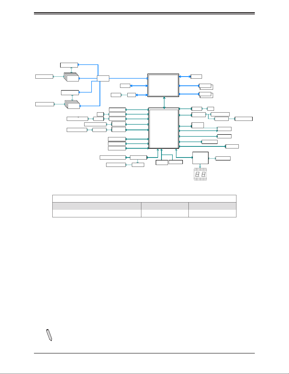
Figure 1-3.
System Block Diagram
Chapter 1: Introduction
PCIe x 8 (in x16) SLOT #5
PCIe x 8 (in x16) SLOT #1
PCIe3.0_x8
8.0GT/s
PCIe3.0_x8
8.0GT/s
1
2
3
4
ASMedia Switch
ASM1480
USB 3.2 Gen2x2 type-c port rear
USB 3.2 Gen2 type-c Header ASM1543
PCIe3.0_x8
8.0GT/s
ASMedia Switch
ASM1480
1
2
PCIe3.0_x8
PCIe3.0_x8
8.0GT/s
3
4
8.0GT/s
PCIe3.0_x8
8.0GT/s
RJ45
ASM1541
2 X USB 3.2 Gen2 Rear Type-A
C9Z490-PGW BLOCK DIAGRAM
SVID
x4 DMI
8GT/s
Intel
PCH-H
Z490
PCH
SPI LPC
TPM1.2 Header
IMVP8
DDR4 (CHA)
2666/2400MHz
DDR4 (CHB)
2666/2400MHz
PCIe3.0_x1 1G LAN1
8GT/s
10Gbps
(SATA-III)
PCIe3.0_x2
8GT/s
PCIe3.0_x2
8GT/s
PCIe3.0_x4
8GT/s
SATA-III 6Gb/s
PLX8747
PCIe x1 SLOT #4
10G LAN2
AQC107
ASM3242
TUSB1002
repeater x2
TUSB1002
repeater
2 X USB 3.2 Gen1 Header
2 X USB 3.2 Gen1 Rear
4 X USB 2.0 Header
Audio Jack/ Aduio Pin Header
PCIe3.0_x16
8.0GT/s
Display Port
DDI1
PS175HDMI 2.0
PCIe3.0_x1
8GT/s
PCIe3.0_x2
8GT/s
PCIe3.0_x4
8GT/s
2 X USB3.2_Gen2
10Gbps
USB3.2_Gen2
10Gbps
2 X USB3.2 Gen1
5Gbps
2 X USB3.2 Gen1
5Gbps
USB2.0
480Mbps
Realtek ALC1220
AMPHead Phone Header
DDI3
INTEL LGA1200
(Socket-H5)
DDI 1
DDI 2
DDI 3
AZALIA
FLASH
SPI 128Mb
PCIe3.0_x8
8.0GT/s
PCIe3.0_x8
8.0GT/s
PCIe x16 SLOT #7
PCIe x16 SLOT #3
Dierences between C9Z490-PG and C9Z490-PGW
C9Z490-PG C9Z490-PGW
PCI-E M.2 E Key for WiFi and Bluetooth No Yes
IMVP8
I219
TUSB1002
repeater x2
ASMedia Switch
ASM1480
CNVi interface
NCT6796D-E
LPC I/O
DIMMA0
DIMMA1
DIMMB0
DIMMB1
4 X SATA-III
RJ45
PCIe3.0_x2
8GT/s
ASM1543
M.2 SOCKET SSD
M.2 SOCKET SSD
COM1 Header
A-epyT raeR 2neG 2.3 BSU2neG 2.3BSU X 2
M.2 key E
for WLAN、BT
USB3.2 Gen2 Rear Type-C
Note: This is a general block diagram and may not exactly represent the features on
your motherboard. Refer to the previous pages for the actual specications of your
motherboard.
17
Page 18

Super C9Z490-PG/-PGW User's Manual
1.2 Processor and Chipset Overview
Built upon the functionality and capability of the 10th Gen Intel Core i9/i7/i5/i3, Pentium, and
Celeron series (LAG1200 processor and the Intel PCH Z490 chipset, the C9Z490-PG/-PGW
motherboard provides system performance, power eciency, and feature sets to address the
needs of next-generation computer users.
With the support of the new Intel Microarchitecture 14nm Process Technology, the
C9Z490-PG/-PGW dramatically increases system performance for a multitude of server
applications.
The Intel PCH Z490 chipset provides support, including the following features:
• DDR4 288-pin memory support
• Direct Media Interface
• Intel Matrix Storage Technology and Intel Rapid Storage Technology
• Dual NAND Interface
• Intel I/O Virtualization (VT-d) Support
• Intel Trusted Execution Technology Support
• PCI-E 3.0 Interface (up to 8 GT/s)
• SATA Controller (up to 6Gb/sec)
• Advanced Host Controller Interface (AHCI)
1.3 Special Features
Recovery from AC Power Loss
The Basic I/O System (BIOS) provides a setting that determines how the system will respond
when AC power is lost and then restored to the system. You can choose for the system to
remain powered o (in which case you must press the power switch to turn it back on), or for
it to automatically return to the power-on state. Refer to the Advanced section for this setting.
The default setting is Last State.
18
Page 19

Chapter 1: Introduction
1.4 System Health Monitoring
Onboard Voltage Monitors
An onboard voltage monitor will scan the voltages of the onboard chipset, memory, CPU,
and battery continuously. Once a voltage becomes unstable, a warning is given, or an error
message is sent to the screen. The user can adjust the voltage thresholds to dene the
sensitivity of the voltage monitor.
Fan Status Monitor with Firmware Control
PC health monitoring in the BIOS can check the RPM status of the cooling fans. The onboard
CPU and chassis fans are controlled by Thermal Management via SIO.
Environmental Temperature Control
The thermal control sensor monitors the CPU temperature in real time and will turn on the
thermal control fan whenever the CPU temperature exceeds a user-dened threshold. The
overheat circuitry runs independently from the CPU. Once the thermal sensor detects that
the CPU temperature is too high, it will automatically turn on the thermal fans to prevent the
CPU from overheating. The onboard chassis thermal circuitry can monitor the overall system
temperature and alert the user when the chassis temperature is too high.
Note: To avoid possible system overheating, please be sure to provide adequate air-
ow to your system.
System Resource Alert
This feature is available when used with SuperDoctor 5 in the Windows OS or in the Linux
environment. SuperDoctor is used to notify the user of certain system events. For example,
you can congure SuperDoctor to provide you with warnings when the system temperature,
CPU temperatures, voltages and fan speeds go beyond a predened range.
19
Page 20

Super C9Z490-PG/-PGW User's Manual
1.5 ACPI Features
ACPI stands for Advanced Conguration and Power Interface. The ACPI specication denes
a exible and abstract hardware interface that provides a standard way to integrate power
management features throughout a computer system, including its hardware, operating
system and application software. This enables the system to automatically turn on and o
peripherals such as CD-ROMs, network cards, hard disk drives and printers.
In addition to enabling operating system-directed power management, ACPI also provides a
generic system event mechanism for Plug and Play, and an operating system-independent
interface for conguration control. ACPI leverages the Plug and Play BIOS data structures,
while providing a processor architecture-independent implementation that is compatible with
appropriate Windows operating systems. For detailed information regarding OS support,
please refer to the Supermicro website.
Slow Blinking LED for Suspend-state Indicator
When the CPU goes into a suspend state, the chassis power LED will start to blink to indicate
that the CPU is in suspend mode. When the user presses any key, the CPU will "wake up,"
and the LED will automatically stop blinking and remain on.
1.6 Power Supply
As with all computer products, a stable power source is necessary for proper and reliable
operation. It is even more important for processors that have high CPU clock rates where
noisy power transmission is present.
The C9Z490-PG/-PGW motherboard accommodates a 24-pin ATX power supply. Although
most power supplies generally meet the specications required by the CPU, some are
inadequate. In addition, one 12V 8-pin power connection is also required to ensure adequate
power supply to the system. Also, your power supply must supply 1.5A for the Ethernet ports.
Warning: To avoid damaging the power supply or the motherboard, be sure to use a
power supply that contains a 24-pin and an 8-pin power connector. Be sure to connect the power supplies to the 24-pin power connector (JPW1), and the 8-pin power
connector (JPW2) on the motherboard. Failure in doing so may void the manufacturer
warranty on your power supply and motherboard.
It is strongly recommended that you use a high quality power supply that meets ATX power
supply Specication 2.02 or later. It must also be SSI compliant. (For more information, please
refer to the website at http://www.ssiforum.org/).
20
Page 21

Chapter 1: Introduction
1.7 Serial Header
The C9Z490-PG/-PGW motherboard supports one serial communication connection. The
COM header can be used for input/output. The UART provides legacy speeds with a baud
rate of up to 115.2 Kbps as well as an advanced speed with baud rates of 250 K, 500 K, or
1 Mb/s, which support high-speed serial communication devices.
1.8 Super I/O
The Super I/O supports one high-speed, 16550 compatible serial communication port (UART).
Each UART includes a 16-byte send/receive FIFO, a programmable baud rate generator,
complete modem control capability and a processor interrupt system. The UART provides
legacy speed with a baud rate of up to 115.2 Kbps as well as an advanced speed with baud
rates of 250 K, 500 K, or 1 Mb/s, which support higher speed modems.
The Super I/O provides functions that comply with ACPI (Advanced Conguration and Power
Interface), which includes support of legacy and ACPI power management through an SMI
or SCI function pin. It also features auto power management to reduce power consumption.
1.9 Intel Optane DC Persistent Memory Overview
10th Gen Intel Core i9/i7/i5/i3, Pentium, and Celeron series processors support new DCPMM
(Optane™ DC Persistent Memory Modules) technology. DCPMM oers data persistence at
higher capacities with lower latencies than the existing memory modules. It also provides
hyper-speed storage capabilities for higher performance computing platforms with exible
conguration options.
21
Page 22

Super C9Z490-PG/-PGW User's Manual
Chapter 2
Installation
2.1 Static-Sensitive Devices
Electrostatic Discharge (ESD) can damage electronic com ponents. To avoid damaging your
system board, it is important to handle it very carefully. The following measures are generally
sucient to protect your equipment from ESD.
Precautions
• Use a grounded wrist strap designed to prevent static discharge.
• Touch a grounded metal object before removing the board from the antistatic bag.
• Handle the motherboard by its edges only; do not touch its components, peripheral chips,
memory modules or gold contacts.
• When handling chips or modules, avoid touching their pins.
• Put the motherboard and peripherals back into their antistatic bags when not in use.
• For grounding purposes, make sure that your computer chassis provides excellent conduc-
tivity between the power supply, the case, the mounting fasteners and the motherboard.
• Use only the correct type of onboard CMOS battery. Do not install the onboard battery
upside down to avoid possible explosion.
Unpacking
The motherboard is shipped in antistatic packaging to avoid static damage. When unpacking
the motherboard, make sure that the person handling it is static protected.
22
Page 23
Chapter 2: Installation
2.2 Processor and Heatsink Installation
The processor (CPU) and processor carrier should be assembled together rst to form
the processor carrier assembly. This will be attached to the heatsink to form the processor
heatsink module (PHM) before being installed onto the CPU socket.
Notes:
• Use ESD protection.
• Unplug the AC power cord from all power supplies after shutting down the system.
• Check that the plastic protective cover is on the CPU socket and none of the socket pins
are bent. If they are, contact your retailer.
• When handling the processor, avoid touching or placing direct pressure on the LGA lands
(gold contacts). Improper installation or socket misalignment can cause serious damage
to the processor or CPU socket, which may require manufacturer repairs.
• Thermal grease is pre-applied on a new heatsink. No additional thermal grease is needed.
• Refer to the Supermicro website for updates on processor support.
• All graphics in this manual are for illustrations only. Your components may look dierent.
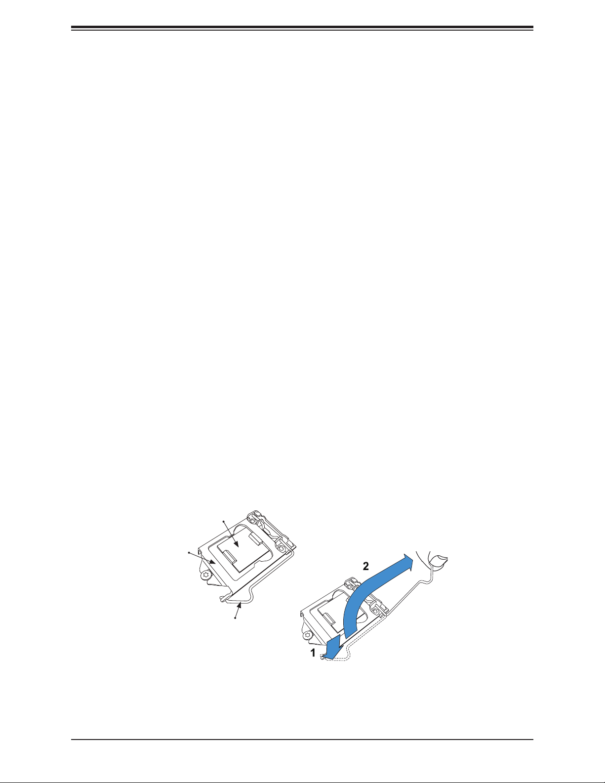
Installing the LGA1200 Processor
1. Press the load lever to release the load plate, which covers the CPU socket, from its
locking position.
Plastic Cap
Load Plate
Load Lever
23
Page 24

Super C9Z490-PG/-PGW User's Manual
2. Gently lift the load lever to open the load plate. Remove the plastic cap.
3. Use your thumb and your index nger to hold the CPU at the North center edge and the
South center edge of the CPU.
North Center Edge
South Center Edge
4. Align the small triangle marker on the CPU to its corresponding triangle marker on the
load bracket. Once it is aligned, carefully lower the CPU straight down into the socket.
(Do not drop the CPU on the socket, or move it horizontally or vertically.)
24
Page 25

Chapter 2: Installation
5. Do not rub the CPU against the surface or against any pins of the socket to avoid
damaging the CPU or the socket.)
6. With the CPU inside the socket, inspect the four corners of the CPU to make sure that
the CPU is properly installed.
7. Use your thumb to gently push the load lever down to the lever lock.
8. Close the load plate with the CPU inside the socket. Lock the "Close 1st" lever rst,
then lock the "Open 1st" lever second. Gently push the load levers down to the lever
locks.
CPU properly
installed
Load lever locked
into place
Attention! You can only install the CPU inside the socket in one direction. Make sure that
it is properly inserted into the CPU socket before closing the load plate. If it doesn't close
properly, do not force it as it may damage your CPU. Instead, open the load plate again
and double-check that the CPU is aligned properly.
25
Page 26
Super C9Z490-PG/-PGW User's Manual
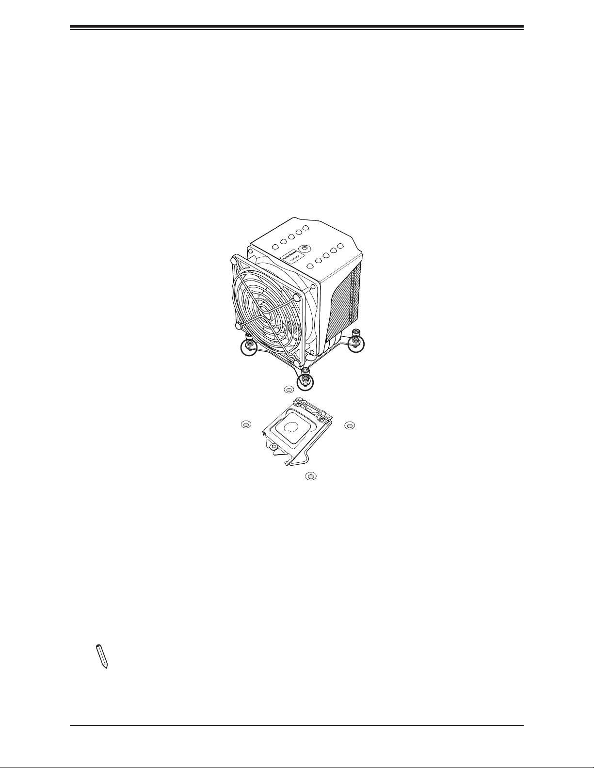
Installing an Active CPU Heatsink with Fan
1. Apply the proper amount of thermal grease to the heatsink.
2. Place the heatsink on top of the CPU so that the four mounting holes on the heatsink
are aligned with those on the retention mechanism.
3. Tighten the screws in the following order:
Screw #4
Screw #2
Screw #3
4. Once the screws are tightened, plug the power connector of cooler into either CPU_
FAN1 or CPU_FAN2 header.
Note 1: Screw #1 is not shown in the illustration.
Note 2: Graphic drawings included in this manual are for reference only. They might
look dierent from the components installed in your system.
26
Page 27

Chapter 2: Installation
Removing an Active CPU Heatsink with Fan
Warning: We do not recommend that the CPU or heatsink be removed. However, if you do
need to remove the heatsink, please follow the instruction below to uninstall the heatsink to
avoid damaging the CPU or other components.
1. Unplug the power cord from the power supply and power connector of cooler from fan
header on the motherboard.
2. Loosen the screws in the order below.
3. Gently wiggle the heatsink to loosen it. Do not use excessive force when wiggling the
heatsink.
Screw #4
Screw #2
Screw #3
4. Once the heatsink is loosened, remove it from the motherboard.
Note: Screw #1 is not shown in the illustration.
27
Page 28
Super C9Z490-PG/-PGW User's Manual
PCH
PLX
Super I/O
LAN Controller
SW1
(CLEAR CMOS)
10G LAN
Controller
+
+
3
1
DESIGNED IN USA
C9Z490-PGW
REV:1.01
BIOS
LICENSE
MAC CODE
MAC CODE
BAR CODE
MH14
JRLED1
MH11
MH10
MH12
MH13
MH15
JSTBY1
JTPM1
HD AUDIO
B1
SP1
JD1
JSD1
SYS_FAN3
USB10/11 (3.2(5Gb))
JPW1
LED18
LED17
LED3
LED2
LED1
JPW2
JI2C2
JI2C1
JL1
LED4
JPAC1
JLED1
JWD1
JPME2
12V_PUMP_PWR1
USB9 (3.2(20Gb))
USB8 (3.2(10Gb))
USB2/3
JF1
BOOT LED
VGA LED
DIMM LED
CPU LED
DP/HDMI
LAN1
AUDIO FP
COM1
USB0/1
PCIE M.2-M1
CPU SLOT1 PCI-E 3.0 X8 (IN X16)
CPU SLOT3 PCI-E 3.0 X16
PCH SLOT4 PCI-E 3.0 X1
CPU SLOT5 PCI-E 3.0 X8 (IN X 16)
I-SATA1
I-SATA0
I-SATA3
I-SATA2
CPU SLOT7 PCI-E 3.0 X16
SYS_FAN2
PCIE M.2-M2
USB12 (3.2(10Gb))
USB6/7 (3.2(10Gb)) USB4/5 (3.2(5Gb))
POWER
BUTTON
DIMMB1
DIMMB2
DIMMA1
DIMMA2
RESET
BUTTON
SYS_FAN1
CPU_FAN1
CLEAR CMOS
CPU_FAN2
LAN2
PCIE M.2-E1
WiFi+BT
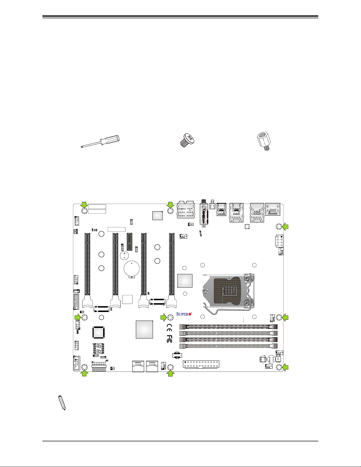
2.3 Motherboard Installation
All motherboards have standard mounting holes to t dierent types of chassis. Make sure
that the locations of all the mounting holes for both the motherboard and the chassis match.
Although a chassis may have both plastic and metal mounting fasteners, metal ones are
highly recommended because they ground the motherboard to the chassis. Make sure that
the metal standos click in or are screwed in tightly.
Tools Needed
Phillips
Screwdriver (1)
Location of Mounting Holes
Phillips Screws (9)
Standos (9)
Only if Needed
Notes: 1. To avoid damaging the motherboard and its components, please do not use
a force greater than 8 lbf-in on each mounting screw during motherboard installation.
2. Some components are very close to the mounting holes. Please take precautionary
measures to avoid damaging these components when installing the motherboard to the
chassis.
28
Page 29
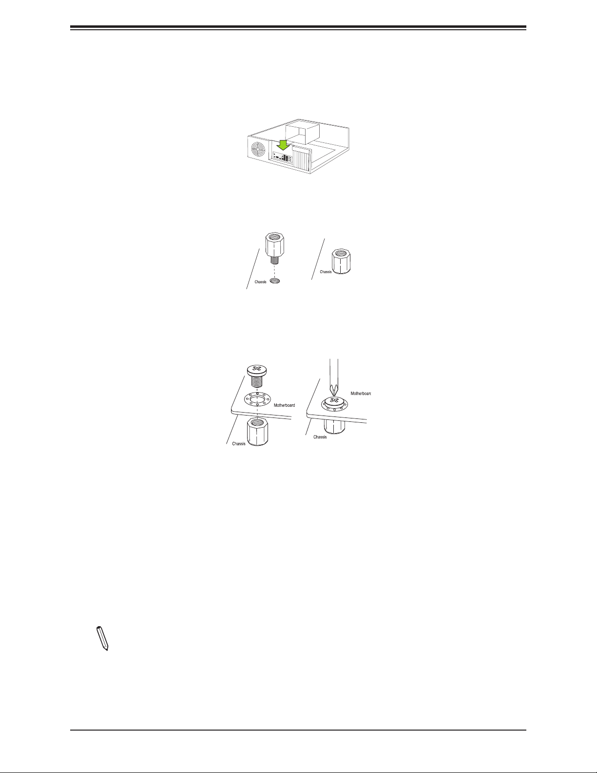
Chapter 2: Installation
Installing the Motherboard
1. Install the I/O shield into the back of the chassis, if applicable.
2. Locate the mounting holes on the motherboard. Refer to the previous page for the
location.
3. Locate the matching mounting holes on the chassis. Align the mounting holes on the
motherboard against the mounting holes on the chassis.
4. Install standos in the chassis as needed.
5. Install the motherboard into the chassis carefully to avoid damaging other motherboard
components.
6. Using the Phillips screwdriver, insert a pan head #6 screw into a mounting hole on the
motherboard and its matching mounting hole on the chassis.
7. Repeat Step 6 to insert #6 screws into all mounting holes.
8. Make sure that the motherboard is securely placed in the chassis.
Note: Images displayed are for illustration only. Your chassis or components might look
dierent from those shown in this manual.
29
Page 30
Super C9Z490-PG/-PGW User's Manual
PCH
PLX
Super I/O
LAN Controller
SW1
(CLEAR CMOS)
10G LAN
Controller
+
+
3
1
DESIGNED IN USA
C9Z490-PGW
REV:1.01
BIOS
LICENSE
MAC CODE
MAC CODE
BAR CODE
MH14
JRLED1
MH11
MH10
MH12
MH13
MH15
JSTBY1
JTPM1
HD AUDIO
B1
SP1
JD1
JSD1
SYS_FAN3
USB10/11 (3.2(5Gb))
JPW1
LED18
LED17
LED3
LED2
LED1
JPW2
JI2C2
JI2C1
JL1
LED4
JPAC1
JLED1
JWD1
JPME2
12V_PUMP_PWR1
USB9 (3.2(20Gb))
USB8 (3.2(10Gb))
USB2/3
JF1
BOOT LED
VGA LED
DIMM LED
CPU LED
DP/HDMI
LAN1
AUDIO FP
COM1
USB0/1
PCIE M.2-M1
CPU SLOT1 PCI-E 3.0 X8 (IN X16)
CPU SLOT3 PCI-E 3.0 X16
PCH SLOT4 PCI-E 3.0 X1
CPU SLOT5 PCI-E 3.0 X8 (IN X 16)
I-SATA1
I-SATA0
I-SATA3
I-SATA2
CPU SLOT7 PCI-E 3.0 X16
SYS_FAN2
PCIE M.2-M2
USB12 (3.2(10Gb))
USB6/7 (3.2(10Gb)) USB4/5 (3.2(5Gb))
POWER
BUTTON
DIMMB1
DIMMB2
DIMMA1
DIMMA2
RESET
BUTTON
SYS_FAN1
CPU_FAN1
CLEAR CMOS
CPU_FAN2
LAN2
PCIE M.2-E1
WiFi+BT
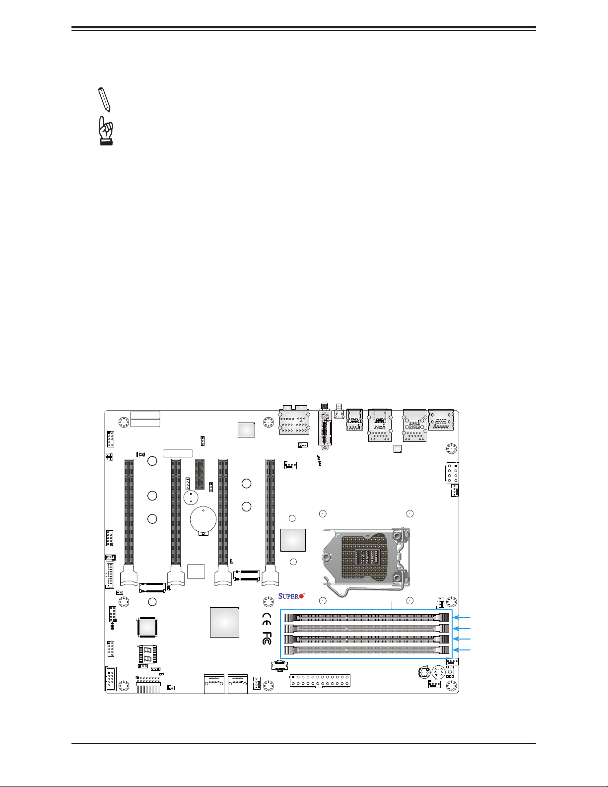
2.4 Memory Support and Installation
Note: Check the Supermicro website for recommended memory modules.
Important: Exercise extreme care when installing or removing DIMM modules to pre-
vent any possible damage.
General Guidelines for Optimizing Memory Performance
• When installing memory modules, the DIMM slots should be populated in the following
order: DIMMA2, DIMMB2, then DIMMA1, DIMMB1.
• Only populate DIMMA1 and DIMMB1 if the extra memory support is needed.
• Always use DDR4 memory of the same type, size and speed.
• Mixed DIMM speeds can be installed. However, all DIMMs will run at the speed of the
slowest DIMM.
• The motherboard will support odd-numbered modules (one or three modules installed).
However, to achieve the best memory performance, a balanced memory population is
recommended.
DIMMA1
DIMMA2
DIMMB1
DIMMB2
30
Page 31
PCH
PLX
Super I/O
LAN Controller
SW1
(CLEAR CMOS)
10G LAN
Controller
+
+
3
1
DESIGNED IN USA
C9Z490-PGW
REV:1.01
BIOS
LICENSE
MAC CODE
MAC CODE
BAR CODE
MH14
JRLED1
MH11
MH10
MH12
MH13
MH15
JSTBY1
JTPM1
HD AUDIO
B1
SP1
JD1
JSD1
SYS_FAN3
USB10/11 (3.2(5Gb))
JPW1
LED18
LED17
LED3
LED2
LED1
JPW2
JI2C2
JI2C1
JL1
LED4
JPAC1
JLED1
JWD1
JPME2
12V_PUMP_PWR1
USB9 (3.2(20Gb))
USB8 (3.2(10Gb))
USB2/3
JF1
BOOT LED
VGA LED
DIMM LED
CPU LED
DP/HDMI
LAN1
AUDIO FP
COM1
USB0/1
PCIE M.2-M1
CPU SLOT1 PCI-E 3.0 X8 (IN X16)
CPU SLOT3 PCI-E 3.0 X16
PCH SLOT4 PCI-E 3.0 X1
CPU SLOT5 PCI-E 3.0 X8 (IN X 16)
I-SATA1
I-SATA0
I-SATA3
I-SATA2
CPU SLOT7 PCI-E 3.0 X16
SYS_FAN2
PCIE M.2-M2
USB12 (3.2(10Gb))
USB6/7 (3.2(10Gb)) USB4/5 (3.2(5Gb))
POWER
BUTTON
DIMMB1
DIMMB2
DIMMA1
DIMMA2
RESET
BUTTON
SYS_FAN1
CPU_FAN1
CLEAR CMOS
CPU_FAN2
LAN2
PCIE M.2-E1
WiFi+BT
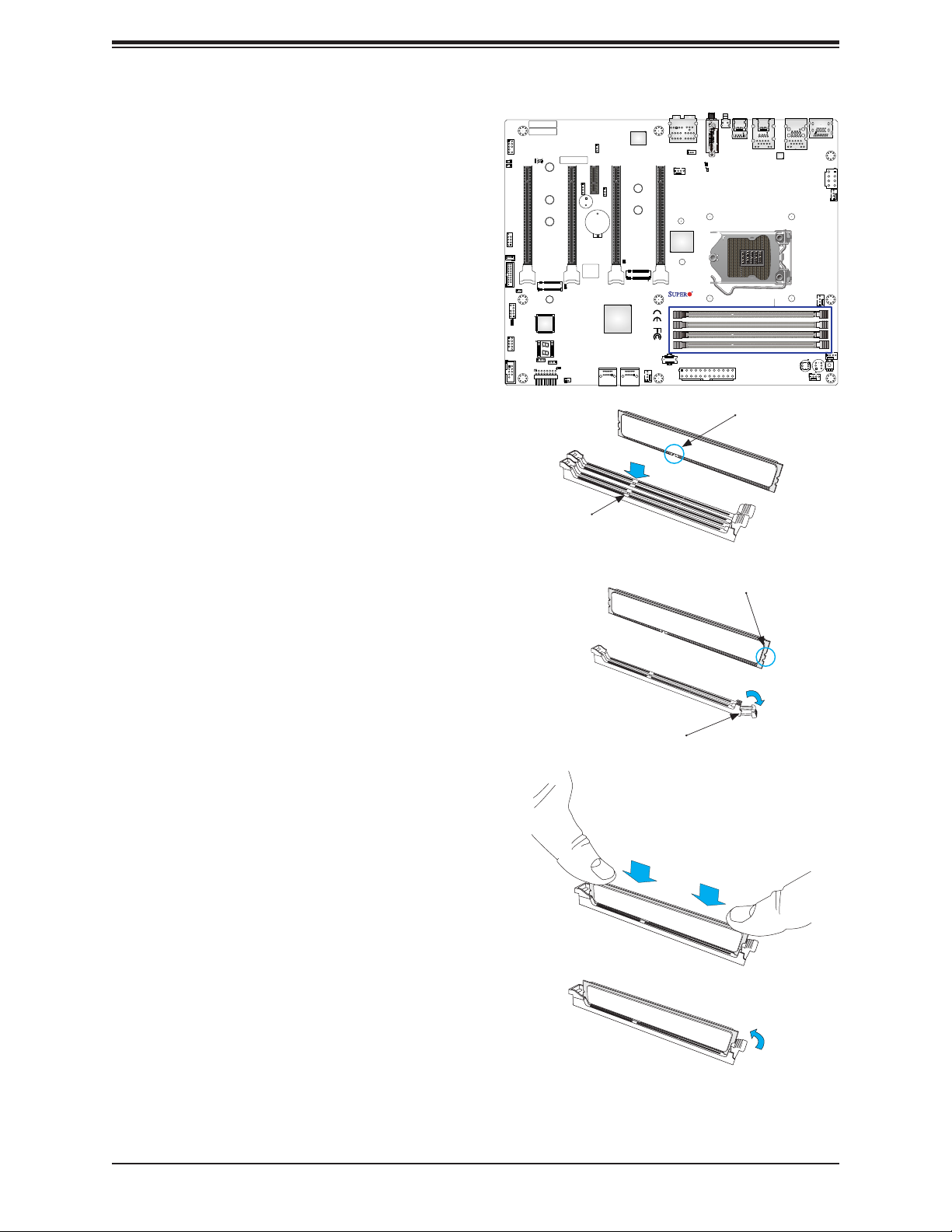
DIMM Installation
1. Insert DIMM modules in the following
rder: DIMMA2, DIMMB2, then DIMMA1,
DIMMB1. For the system to work properly,
use memory modules of the same type
and speed.
2. Align the DIMM module key with the
receptive point on the single-latch DIMM
slot.
3. Push the release tab outwards to unlock
the slot.
4. Align the notch on the end of the module
against the receptive point on the end of
the slot.
Chapter 2: Installation
5. Press both ends of the module straight
Receptive Point
down into the slot until the module snaps
into place.
Notch
6. Push the release tab to the lock position to
secure the module into the slot.
DIMM Removal
Reverse the steps above to remove the DIMM
modules from the motherboard.
31
Release Tab
Push both ends straight
down into the memory slot.
Page 32

Super C9Z490-PG/-PGW User's Manual
2.5 M.2 Installation (optional)
Two M.2 M key sockets are supported by the C9Z490-PG/-PGW. M.2 devices are used for
solid state storage and internal expansion. Follow the steps below in order to install an M.2
device.
1. Locate and remove the retaining screws on the M.2
heatsinks.
2. With the heatsink removed, locate the bundled
stando depends on the length of M.2 device if
necessary.
Note:
the 2280 and 22110 mounting holes and designed for the heatsink installation. To plug the
smaller M.2 device, please using other stando
bundled in the motherboard package.
3. Carefully plug the M.2 device into the M.2 socket
and lower the semi-circle notched end onto the
stando.
Two standos have been pre-installed in
32
Page 33

4. Remove the M.2 heatsink thermal pad cover.
5. Replace the M.2 heatsink and the retaining screws.
Tighten the screws to secure the heatsink into place.
Chapter 2: Installation
Notes:
1. DO NOT install the bounded M.2 heatsink (refer to step 4 and 5) if the M.2 device
has a heatsink installed.
2. Please assemble the M.2 heatsink back to the motherboard once the M.2 device
has been removed.
3. Beware of the direction when assembling the heatsink (refer to step 5).
33
Page 34

Super C9Z490-PG/-PGW User's Manual
PCH
PLX
Super I/O
LAN Controller
SW1
(CLEAR CMOS)
10G LAN
Controller
+
+
3
1
DESIGNED IN USA
C9Z490-PGW
REV:1.01
BIOS
LICENSE
MAC CODE
MAC CODE
BAR CODE
MH14
JRLED1
MH11
MH10
MH12
MH13
MH15
JSTBY1
JTPM1
HD AUDIO
B1
SP1
JD1
JSD1
SYS_FAN3
USB10/11 (3.2(5Gb))
JPW1
LED18
LED17
LED3
LED2
LED1
JPW2
JI2C2
JI2C1
JL1
LED4
JPAC1
JLED1
JWD1
JPME2
12V_PUMP_PWR1
USB9 (3.2(20Gb))
USB8 (3.2(10Gb))
USB2/3
JF1
BOOT LED
VGA LED
DIMM LED
CPU LED
DP/HDMI
LAN1
AUDIO FP
COM1
USB0/1
PCIE M.2-M1
CPU SLOT1 PCI-E 3.0 X8 (IN X16)
CPU SLOT3 PCI-E 3.0 X16
PCH SLOT4 PCI-E 3.0 X1
CPU SLOT5 PCI-E 3.0 X8 (IN X 16)
I-SATA1
I-SATA0
I-SATA3
I-SATA2
CPU SLOT7 PCI-E 3.0 X16
SYS_FAN2
PCIE M.2-M2
USB12 (3.2(10Gb))
USB6/7 (3.2(10Gb)) USB4/5 (3.2(5Gb))
POWER
BUTTON
DIMMB1
DIMMB2
DIMMA1
DIMMA2
RESET
BUTTON
SYS_FAN1
CPU_FAN1
CLEAR CMOS
CPU_FAN2
LAN2
PCIE M.2-E1
WiFi+BT
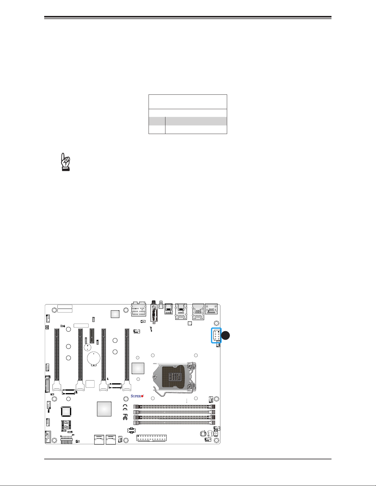
2.6 Rear I/O Ports
Refer to Figure 2-1 below for the locations and descriptions of the various I/O ports on the
rear of the motherboard.
Figure 2-1. I/O Port Locations and Denitions
13
15
16
17
18
3
6
1
9
2
4
5
# Description # Description
1 DisplayPort 10 USB9: USB 3.2 Gen 2x2 (Type C)
2 HDMI Port 11 SW1: CLEAR CMOS
3 Ethernet RJ45 10GbE Port 1 12 WiFi+BT (C9Z490-PGW only)
4 USB4: USB 3.2 Gen 1 (Type A) 13 Center/LFE Out
5 USB5: USB 3.2 Gen 1 (Type A) 14 Surround Out
6 Ethernet RJ45 1GbE Port 2 15 S/PDIF Out
7 USB6: USB 3.2 Gen 2 (Type A) 16 Line In
8 USB7: USB 3.2 Gen 2 (Type C) 17 Line Out
9 USB8: USB 3.2 Gen 2 (Type A) 18 Mic In
7
8
Rear I/O Ports
10 11 12 14
34
Page 35

Chapter 2: Installation
PCH
PLX
Super I/O
LAN Controller
SW1
(CLEAR CMOS)
10G LAN
Controller
+
+
3
1
DESIGNED IN USA
C9Z490-PGW
REV:1.01
BIOS
LICENSE
MAC CODE
MAC CODE
BAR CODE
MH14
JRLED1
MH11
MH10
MH12
MH13
MH15
JSTBY1
JTPM1
HD AUDIO
B1
SP1
JD1
JSD1
SYS_FAN3
USB10/11 (3.2(5Gb))
JPW1
LED18
LED17
LED3
LED2
LED1
JPW2
JI2C2
JI2C1
JL1
LED4
JPAC1
JLED1
JWD1
JPME2
12V_PUMP_PWR1
USB9 (3.2(20Gb))
USB8 (3.2(10Gb))
USB2/3
JF1
BOOT LED
VGA LED
DIMM LED
CPU LED
DP/HDMI
LAN1
AUDIO FP
COM1
USB0/1
PCIE M.2-M1
CPU SLOT1 PCI-E 3.0 X8 (IN X16)
CPU SLOT3 PCI-E 3.0 X16
PCH SLOT4 PCI-E 3.0 X1
CPU SLOT5 PCI-E 3.0 X8 (IN X 16)
I-SATA1
I-SATA0
I-SATA3
I-SATA2
CPU SLOT7 PCI-E 3.0 X16
SYS_FAN2
PCIE M.2-M2
USB12 (3.2(10Gb))
USB6/7 (3.2(10Gb)) USB4/5 (3.2(5Gb))
POWER
BUTTON
DIMMB1
DIMMB2
DIMMA1
DIMMA2
RESET
BUTTON
SYS_FAN1
CPU_FAN1
CLEAR CMOS
CPU_FAN2
LAN2
PCIE M.2-E1
WiFi+BT
Universal Serial Bus (USB) Ports
Two USB 3.2 Gen 1 Type A ports (USB4/5), two USB 3.2 Gen 2 Type A ports (USB6/8), one
USB 3.2 Gen 2 Type C port (USB7), and one USB 3.2 Gen 2x2 Type C port (USB9) are
located on the I/O back panel. In addition, four front panel USB 2.0 headers (USB0/1, 2/3),
one USB 3.2 Gen 1 header (USB10/11), and one USB 3.2 Gen 2 20-pin connector (USB12)
are also located on the motherboard to provide front chassis access using USB cables (not
included). Refer to the tables below for pin denitions.
Front Panel USB0/1, 2/3 (2.0)
Pin Denitions
Pin# Denition Pin# Denition
1 +5V 2 +5V
3 USB_PN2 4 USB_PN3
5 USB_PP2 6 USB_PP3
7 Ground 8 Ground
9 Key 10 Ground
Pin# Pin# Signal Name Description
1 19 VBUS Power
2 18 StdA_SSRX- USB 2.0 Dierential Pair
3 17 StdA_SSRX+
4 13 Ground Ground of PWR Return
5 15 StdA_SSTX- SuperSpeed Receiver
Front Panel USB10/11 (3.2 Gen 1)
Pin Denitions
6 14 StdA_SSTX+ Dierential Pair
7 16 GND_DRAIN Ground for Signal Return
8 12 D- SuperSpeed Transmitter
9 11 D+ Dierential Pair
Front Panel USB 12 (3.2 Gen 2)
Pin Denitions
Pin# Denition Pin# Denition Pin# Denition
1 VBUS 5 RX1+ 9 NC 13 TX2- 17 GND
2 TX1+ 6 RX1- 10 NC 14 GND 18 D-
3 TX1- 7 VBUS 11 VBUS 15 RX2+ 19 D+
4 GND 8 CC1 12 TX2+ 16 RX2- 20 CC2
Up
674
Down
3
5
1
8
2
1. USB0/1 (USB 2.0)
2. USB2/3 (USB 2.0)
3. USB4/5 (USB 3.2 Gen 1)
4. USB6 (USB 3.2 Gen 2)
5. USB7 (USB 3.2 Gen 2)
6. USB8 (USB 3.2 Gen 2)
7. USB9 (USB 3.2 Gen 2x2)
8. USB10/11 (USB 3.2 Gen 1)
9. USB12 (USB 3.2 Gen 2)
9
35
Page 36

Super C9Z490-PG/-PGW User's Manual
Back Panel High Denition Audio (HD Audio)
This motherboard features a 7.1+2 Channel High Denition Audio (HDA) codec that provides
10 DAC channels. The HD Audio connections simultaneously supports multiple-streaming 7.1
sound playback with 2 channels of independent stereo output through the front panel stereo
out for front, rear, center and subwoofer speakers. Use the Advanced software included in
the CD-ROM with your motherboard to enable this function.
Audio Conguration
2 Channel 4.1 Channel 5.1 Channel 7.1 Channel
1 Orange (Center/LFE Out) Center/Subwoofer Center/Subwoofer
2 Black (Surround) Rear Speaker Out Rear Speaker Out Rear Speaker Out
Light Blue
3
(Line In/Side Speaker Out)
Lime
4
(Line Out/Front Speaker Out)
5 Pink (Mic In) Mic In Mic In Mic In Mic In
Line In Line In Line In Side Speaker Out
Line Out Front Speaker Out Front Speaker Out Front Speaker Out
36
123
1. Center/LFE Out
2. Surround Out
3. Line In
4. Line Out
4
5
5. Mic In
Page 37

Chapter 2: Installation
DisplayPort Port
DisplayPort, developed by the VESA consortium, delivers digital display at a fast refresh rate.
It can connect to virtually any display device using a DisplayPort adapter for devices, such
as VGA, DVI, and HDMI.
HDMI Port
One HDMI 2.0a (High-Denition Multimedia Interface) port is located on the I/O back panel.
This port is used to display both high denition video and digital sound through an HDMI
capable display, using a single HDMI cable (not included).
LAN Ports
Two RJ45 Ethernet LAN ports (LAN1/LAN2) are located on the I/O back panel to provide
network connections. These ports accept RJ45 type cables.
Note: Please refer to Section 2.10 for LAN LED information.
LAN1 Port
Pin Denitions
Pin# Denition Pin# Denition
19 SGND 28 SGND
20 TD0+ 29 Link 1000 LED (Yellow, +3V3SB)
21 TD0- 30 Link 100 LED (Green, +3V3SB)
22 TD1+ 31 P3V3SB
23 TD1- 32 Act LED
24 TD2+ 33 Ground
25 TD2- 34 Ground
26 TD3+ 35 Ground
27 TD3- 36 Ground
3
4
1
Pin# Denition Pin# Denition
10 SGND 19 SGND
11 TD0+ 20 Link 1000 LED (Yellow, +3V3SB)
12 TD0- 21 Link 100 LED (Green, +3V3SB)
13 TD1+ 22 P3V3SB
14 TD1- 23 Act LED
15 TD2+ 24 Ground
16 TD2- 25 Ground
17 TD3+ 26 Ground
18 TD3- 27 Ground
LAN2 Port
Pin Denitions
1. DisplayPort Port
2. HDMI Port
3. LAN1
4. LAN2
2
37
Page 38

Super C9Z490-PG/-PGW User's Manual
PCH
PLX
Super I/O
LAN Controller
SW1
(CLEAR CMOS)
10G LAN
Controller
+
+
3
1
DESIGNED IN USA
C9Z490-PGW
REV:1.01
BIOS
LICENSE
MAC CODE
MAC CODE
BAR CODE
MH14
JRLED1
MH11
MH10
MH12
MH13
MH15
JSTBY1
JTPM1
HD AUDIO
B1
SP1
JD1
JSD1
SYS_FAN3
USB10/11 (3.2(5Gb))
JPW1
LED18
LED17
LED3
LED2
LED1
JPW2
JI2C2
JI2C1
JL1
LED4
JPAC1
JLED1
JWD1
JPME2
12V_PUMP_PWR1
USB9 (3.2(20Gb))
USB8 (3.2(10Gb))
USB2/3
JF1
BOOT LED
VGA LED
DIMM LED
CPU LED
DP/HDMI
LAN1
AUDIO FP
COM1
USB0/1
PCIE M.2-M1
CPU SLOT1 PCI-E 3.0 X8 (IN X16)
CPU SLOT3 PCI-E 3.0 X16
PCH SLOT4 PCI-E 3.0 X1
CPU SLOT5 PCI-E 3.0 X8 (IN X 16)
I-SATA1
I-SATA0
I-SATA3
I-SATA2
CPU SLOT7 PCI-E 3.0 X16
SYS_FAN2
PCIE M.2-M2
USB12 (3.2(10Gb))
USB6/7 (3.2(10Gb)) USB4/5 (3.2(5Gb))
POWER
BUTTON
DIMMB1
DIMMB2
DIMMA1
DIMMA2
RESET
BUTTON
SYS_FAN1
CPU_FAN1
CLEAR CMOS
CPU_FAN2
LAN2
PCIE M.2-E1
WiFi+BT
2.7 Front Control Panel
JF1 contains header pins for various buttons and indicators that are normally located on a
control panel at the front of the chassis. These connectors are designed specically for use
with Supermicro chassis. Refer to the gure below for the descriptions of the front control
panel buttons and LED indicators.
Note: You may connect the JF1 using the bundled S-Connector. The S-Connector is a
plug designed to connect the front control panel header on the motherboard and front
control panel cables of chassis. Please align the printed indications on the S-Connector
with the corresponding pins on JF1 when plugging in. Refer to the checklist table in
Section 1.1 and contact Supermicro for more detailed connector information.
1615
POWER LED (-)
HDD LED (-)
NIC1 LED (-)
NIC2 LED (-)
Overheat/
Fan Fail LED (-)
X
Ground
Ground
1
Figure 2-2. JF1 Header Pins
POWER LED (+)
HDD LED (+)
NIC1 LED (+)
NIC2 LED (+)
Overheat/
Fan Fail LED (+)
X
Reset
PWR
2
38
Reset Button
Power Button
Page 39

Chapter 2: Installation
Power LED
The Power LED connection is located on pins 15 and 16 of JF1. Refer to the table below
for pin denitions.
Power LED
Pin Denitions (JF1)
Pin# Denition
15 Power LED
16 Vcc
HDD LED
The HDD LED connection is located on pins 13 and 14 of JF1. Attach a cable here to indicate
the status of HDD-related activities, including IDE and SATA activities. Refer to the table
below for pin denitions.
1
POWER LED (-)
2
HDD LED (-)
NIC1 LED (-)
NIC2 LED (-)
Overheat/
Fan Fail LED (-)
HDD LED
Pin Denitions (JF1)
Pin# Denition
13 HDD LED
14 Vcc
1615
POWER LED (+)
HDD LED (+)
1. Power LED
2. HDD LED
NIC1 LED (+)
NIC2 LED (+)
Overheat/
Fan Fail LED (+)
X
X
Ground
Ground
Reset
PWR
2
1
Reset Button
Power Button
39
Page 40

Super C9Z490-PG/-PGW User's Manual
NIC1/NIC2 (LAN1/LAN2) LED
The NIC (Network Interface Controller) LED connection for LAN1/LAN2 is located on pins 9/11
and 10/12 of JF1. Attach an LED indicator to this header to display network activity. Refer to
the table below for pin denitions.
NIC1/NIC2 LED
Pin Denitions (JF1)
Pin# Denition
9/11 NIC2/NIC1 LED
10/12 Vcc
Overheat (OH)/Fan Fail LED
Connect an LED cable to OH/Fan Fail connections on pins 7 and 8 of JF1 to provide warnings
for chassis overheat/fan failure. Refer to the tables below for pin denitions.
POWER LED (-)
HDD LED (-)
1
NIC1 LED (-)
2
NIC2 LED (-)
Overheat/
3
Fan Fail LED (-)
OH/Fan Fail LED
Pin Denitions (JF1)
Pin# Denition
7 OH/Fan Fail LED
8 Vcc
1615
X
POWER LED (+)
HDD LED (+)
NIC1 LED (+)
NIC2 LED (+)
Overheat/
Fan Fail LED (+)
X
OH/Fan Fail Indicator
Pin Denitions (JF1)
State Denition
O Normal
On Overheat
Flashing Fan Fail
1. NIC1 LED
2. NIC2 LED
3. OH/Fan Fail LED
Ground
Ground
Reset
PWR
2
1
Reset Button
Power Button
40
Page 41

Chapter 2: Installation
Reset Button
The Reset Button connection is located on pins 3 and 4 of JF1. Attach it to a hardware reset
switch on the computer case to reset the system. Refer to the table below for pin denitions.
Reset Button
Pin Denitions (JF1)
Pin# Denition
3 Ground
4 Reset Button
Power Button
The Power Button connection is located on pins 1 and 2 of JF1. Momentarily contacting both
pins will power on/o the system. To turn o the power in the suspend mode, press the button
for at least four seconds. Refer to the table below for pin denitions.
POWER LED (-)
HDD LED (-)
NIC1 LED (-)
NIC2 LED (-)
Overheat/
Fan Fail LED (-)
Power Button
Pin Denitions (JF1)
Pin# Denition
1 Ground
2 Power Button
1615
POWER LED (+)
HDD LED (+)
1. Reset Button
2. Power Button
NIC1 LED (+)
NIC2 LED (+)
Overheat/
Fan Fail LED (+)
X
X
Ground
Ground
Reset
PWR
2
1
Reset Button
Power Button
1
2
41
Page 42

Super C9Z490-PG/-PGW User's Manual
PCH
PLX
Super I/O
LAN Controller
SW1
(CLEAR CMOS)
10G LAN
Controller
+
+
3
1
DESIGNED IN USA
C9Z490-PGW
REV:1.01
BIOS
LICENSE
MAC CODE
MAC CODE
BAR CODE
MH14
JRLED1
MH11
MH10
MH12
MH13
MH15
JSTBY1
JTPM1
HD AUDIO
B1
SP1
JD1
JSD1
SYS_FAN3
USB10/11 (3.2(5Gb))
JPW1
LED18
LED17
LED3
LED2
LED1
JPW2
JI2C2
JI2C1
JL1
LED4
JPAC1
JLED1
JWD1
JPME2
12V_PUMP_PWR1
USB9 (3.2(20Gb))
USB8 (3.2(10Gb))
USB2/3
JF1
BOOT LED
VGA LED
DIMM LED
CPU LED
DP/HDMI
LAN1
AUDIO FP
COM1
USB0/1
PCIE M.2-M1
CPU SLOT1 PCI-E 3.0 X8 (IN X16)
CPU SLOT3 PCI-E 3.0 X16
PCH SLOT4 PCI-E 3.0 X1
CPU SLOT5 PCI-E 3.0 X8 (IN X 16)
I-SATA1
I-SATA0
I-SATA3
I-SATA2
CPU SLOT7 PCI-E 3.0 X16
SYS_FAN2
PCIE M.2-M2
USB12 (3.2(10Gb))
USB6/7 (3.2(10Gb)) USB4/5 (3.2(5Gb))
POWER
BUTTON
DIMMB1
DIMMB2
DIMMA1
DIMMA2
RESET
BUTTON
SYS_FAN1
CPU_FAN1
CLEAR CMOS
CPU_FAN2
LAN2
PCIE M.2-E1
WiFi+BT
2.8 Connectors
This section provides brief descriptions and pinout denitions for onboard headers and
connectors. Be sure to use the correct cable for each header or connector.
Power Connections
ATX Power Supply Connector
The 24-pin power supply connector (JPW1) meets the ATX SSI EPS 12V specication. You
must also connect the 8-pin (JPW2) processor power connector to the power supply.
ATX Power 24-pin Connector
Pin Denitions
Pin# Denition Pin# Denition
13 +3.3V 1 +3.3V
14 -12V 2 +3.3V
15 Ground 3 Ground
16 PS_ON 4 +5V
17 Ground 5 Ground
18 Ground 6 +5V
19 Ground 7 Ground
20 Res (NC) 8 PWR_OK
21 +5V 9 5VSB
22 +5V 10 +12V
23 +5V 11 +12V
24 Ground 12 +3.3V
Required Connection
1. JPW1
1
42
Page 43
Chapter 2: Installation
PCH
PLX
Super I/O
LAN Controller
SW1
(CLEAR CMOS)
10G LAN
Controller
+
+
3
1
DESIGNED IN USA
C9Z490-PGW
REV:1.01
BIOS
LICENSE
MAC CODE
MAC CODE
BAR CODE
MH14
JRLED1
MH11
MH10
MH12
MH13
MH15
JSTBY1
JTPM1
HD AUDIO
B1
SP1
JD1
JSD1
SYS_FAN3
USB10/11 (3.2(5Gb))
JPW1
LED18
LED17
LED3
LED2
LED1
JPW2
JI2C2
JI2C1
JL1
LED4
JPAC1
JLED1
JWD1
JPME2
12V_PUMP_PWR1
USB9 (3.2(20Gb))
USB8 (3.2(10Gb))
USB2/3
JF1
BOOT LED
VGA LED
DIMM LED
CPU LED
DP/HDMI
LAN1
AUDIO FP
COM1
USB0/1
PCIE M.2-M1
CPU SLOT1 PCI-E 3.0 X8 (IN X16)
CPU SLOT3 PCI-E 3.0 X16
PCH SLOT4 PCI-E 3.0 X1
CPU SLOT5 PCI-E 3.0 X8 (IN X 16)
I-SATA1
I-SATA0
I-SATA3
I-SATA2
CPU SLOT7 PCI-E 3.0 X16
SYS_FAN2
PCIE M.2-M2
USB12 (3.2(10Gb))
USB6/7 (3.2(10Gb)) USB4/5 (3.2(5Gb))
POWER
BUTTON
DIMMB1
DIMMB2
DIMMA1
DIMMA2
RESET
BUTTON
SYS_FAN1
CPU_FAN1
CLEAR CMOS
CPU_FAN2
LAN2
PCIE M.2-E1
WiFi+BT
8-Pin Power Connector
JPW2 is an 8-pin 12V DC power input for the CPU that must be connected to the power
supply. Refer to the table below for pin denitions.
8-pin Power
Pin Denitions
Pin# Denition
1 - 4 Ground
5 - 8 +12V
Required Connection
Important: To provide adequate power supply to the motherboard, be sure to connect
the 24-pin ATX PWR and the 8-pin PWR connectors to the power supply. Failure to
do so may void the manufacturer warranty on your power supply and motherboard.
1. JPW2
1
43
Page 44

Super C9Z490-PG/-PGW User's Manual
PCH
PLX
Super I/O
LAN Controller
SW1
(CLEAR CMOS)
10G LAN
Controller
+
+
3
1
DESIGNED IN USA
C9Z490-PGW
REV:1.01
BIOS
LICENSE
MAC CODE
MAC CODE
BAR CODE
MH14
JRLED1
MH11
MH10
MH12
MH13
MH15
JSTBY1
JTPM1
HD AUDIO
B1
SP1
JD1
JSD1
SYS_FAN3
USB10/11 (3.2(5Gb))
JPW1
LED18
LED17
LED3
LED2
LED1
JPW2
JI2C2
JI2C1
JL1
LED4
JPAC1
JLED1
JWD1
JPME2
12V_PUMP_PWR1
USB9 (3.2(20Gb))
USB8 (3.2(10Gb))
USB2/3
JF1
BOOT LED
VGA LED
DIMM LED
CPU LED
DP/HDMI
LAN1
AUDIO FP
COM1
USB0/1
PCIE M.2-M1
CPU SLOT1 PCI-E 3.0 X8 (IN X16)
CPU SLOT3 PCI-E 3.0 X16
PCH SLOT4 PCI-E 3.0 X1
CPU SLOT5 PCI-E 3.0 X8 (IN X 16)
I-SATA1
I-SATA0
I-SATA3
I-SATA2
CPU SLOT7 PCI-E 3.0 X16
SYS_FAN2
PCIE M.2-M2
USB12 (3.2(10Gb))
USB6/7 (3.2(10Gb)) USB4/5 (3.2(5Gb))
POWER
BUTTON
DIMMB1
DIMMB2
DIMMA1
DIMMA2
RESET
BUTTON
SYS_FAN1
CPU_FAN1
CLEAR CMOS
CPU_FAN2
LAN2
PCIE M.2-E1
WiFi+BT
Headers
Fan Headers
There are ve 4-pin fan headers (CPU_FAN1 ~ CPU_FAN2, SYS_FAN1 ~ SYS_FAN3) on
the motherboard. Although Pins 1-3 of the system fan headers are backwards compatible
with the traditional 3-pin fans, the 4-pin fans are recommended to take advantage of the fan
speed control. This allows fan speeds to be automatically adjusted based on the motherboard
temperature. Refer to the table below for pin denitions.
Fan Headers
Pin Denitions
Pin# Denition
1 Ground (Black)
2 2A/+12V (Red)
3 Tachometer
4 PWM_Control
Pump Power Header
This motherboard has one +12V header for optional CPU liquid cooling systems. When using
a liquid cooling system, attach the pump power cable to the 12V_PUMP_PWR1 header.
Pump Power Header
Pin Denitions
Pin# Denition
1 Ground (Black)
2 2A/+12V (Red)
3 N/A
4 N/A
1. CPU_FAN1
2. CPU_FAN2
5
4
44
2
3
3. SYS_FAN1
4. SYS_FAN2
5. SYS_FAN3
6. 12V_PUMP_PWR1
6
1
Page 45

Chapter 2: Installation
PCH
PLX
Super I/O
LAN Controller
SW1
(CLEAR CMOS)
10G LAN
Controller
+
+
3
1
DESIGNED IN USA
C9Z490-PGW
REV:1.01
BIOS
LICENSE
MAC CODE
MAC CODE
BAR CODE
MH14
JRLED1
MH11
MH10
MH12
MH13
MH15
JSTBY1
JTPM1
HD AUDIO
B1
SP1
JD1
JSD1
SYS_FAN3
USB10/11 (3.2(5Gb))
JPW1
LED18
LED17
LED3
LED2
LED1
JPW2
JI2C2
JI2C1
JL1
LED4
JPAC1
JLED1
JWD1
JPME2
12V_PUMP_PWR1
USB9 (3.2(20Gb))
USB8 (3.2(10Gb))
USB2/3
JF1
BOOT LED
VGA LED
DIMM LED
CPU LED
DP/HDMI
LAN1
AUDIO FP
COM1
USB0/1
PCIE M.2-M1
CPU SLOT1 PCI-E 3.0 X8 (IN X16)
CPU SLOT3 PCI-E 3.0 X16
PCH SLOT4 PCI-E 3.0 X1
CPU SLOT5 PCI-E 3.0 X8 (IN X 16)
I-SATA1
I-SATA0
I-SATA3
I-SATA2
CPU SLOT7 PCI-E 3.0 X16
SYS_FAN2
PCIE M.2-M2
USB12 (3.2(10Gb))
USB6/7 (3.2(10Gb)) USB4/5 (3.2(5Gb))
POWER
BUTTON
DIMMB1
DIMMB2
DIMMA1
DIMMA2
RESET
BUTTON
SYS_FAN1
CPU_FAN1
CLEAR CMOS
CPU_FAN2
LAN2
PCIE M.2-E1
WiFi+BT
Chassis Intrusion Header
A Chassis Intrusion header is located at JL1 on the motherboard. Attach the appropriate cable
from the chassis to inform you of a chassis intrusion when the chassis is opened.
Chassis Intrusion Header
Pin Denitions
Pin# Denition
1 Intrusion Input
2 Ground
Speaker Header
On JD1 Header, pins 3 and 4 are used for the internal speaker. Close pins 3 and 4 with a
cap to use the onboard speaker. If you wish to use an external speaker, close pins 1-4 with
a cable. Refer to the table below for pin denitions.
1
2
Speaker Header
Pin Denitions
Pin# Denition
3-4 Internal Speaker
1-4 External Speaker
1. JL1
2. JD1
45
Page 46

Super C9Z490-PG/-PGW User's Manual
PCH
PLX
Super I/O
LAN Controller
SW1
(CLEAR CMOS)
10G LAN
Controller
+
+
3
1
DESIGNED IN USA
C9Z490-PGW
REV:1.01
BIOS
LICENSE
MAC CODE
MAC CODE
BAR CODE
MH14
JRLED1
MH11
MH10
MH12
MH13
MH15
JSTBY1
JTPM1
HD AUDIO
B1
SP1
JD1
JSD1
SYS_FAN3
USB10/11 (3.2(5Gb))
JPW1
LED18
LED17
LED3
LED2
LED1
JPW2
JI2C2
JI2C1
JL1
LED4
JPAC1
JLED1
JWD1
JPME2
12V_PUMP_PWR1
USB9 (3.2(20Gb))
USB8 (3.2(10Gb))
USB2/3
JF1
BOOT LED
VGA LED
DIMM LED
CPU LED
DP/HDMI
LAN1
AUDIO FP
COM1
USB0/1
PCIE M.2-M1
CPU SLOT1 PCI-E 3.0 X8 (IN X16)
CPU SLOT3 PCI-E 3.0 X16
PCH SLOT4 PCI-E 3.0 X1
CPU SLOT5 PCI-E 3.0 X8 (IN X 16)
I-SATA1
I-SATA0
I-SATA3
I-SATA2
CPU SLOT7 PCI-E 3.0 X16
SYS_FAN2
PCIE M.2-M2
USB12 (3.2(10Gb))
USB6/7 (3.2(10Gb)) USB4/5 (3.2(5Gb))
POWER
BUTTON
DIMMB1
DIMMB2
DIMMA1
DIMMA2
RESET
BUTTON
SYS_FAN1
CPU_FAN1
CLEAR CMOS
CPU_FAN2
LAN2
PCIE M.2-E1
WiFi+BT
Power LED Header
An onboard Power LED header is located at JLED1. This Power LED header is connected
to the Front Control Panel located at JF1 to indicate the status of system power. Refer to the
table below for pin denitions.
Power LED Header
Pin Denitions
Pin# Denition
1 VCC
2 Connection to PWR LED in JF1
3 Connection to PWR LED in JF1
White Light LED Header
This 4-pin connector provides the connection to white light LED board inside the I/O cover. It
is located at JRLED1 on the motherboard. Refer to the table below for pin denitions.
1
White Light LED Header
Pin Denitions
Pin# Denition
1 VCC
2 NC
3 NC
4 Ground
1. JLED1
2
46
2. JRLED1
Page 47

Chapter 2: Installation
PCH
PLX
Super I/O
LAN Controller
SW1
(CLEAR CMOS)
10G LAN
Controller
+
+
3
1
DESIGNED IN USA
C9Z490-PGW
REV:1.01
BIOS
LICENSE
MAC CODE
MAC CODE
BAR CODE
MH14
JRLED1
MH11
MH10
MH12
MH13
MH15
JSTBY1
JTPM1
HD AUDIO
B1
SP1
JD1
JSD1
SYS_FAN3
USB10/11 (3.2(5Gb))
JPW1
LED18
LED17
LED3
LED2
LED1
JPW2
JI2C2
JI2C1
JL1
LED4
JPAC1
JLED1
JWD1
JPME2
12V_PUMP_PWR1
USB9 (3.2(20Gb))
USB8 (3.2(10Gb))
USB2/3
JF1
BOOT LED
VGA LED
DIMM LED
CPU LED
DP/HDMI
LAN1
AUDIO FP
COM1
USB0/1
PCIE M.2-M1
CPU SLOT1 PCI-E 3.0 X8 (IN X16)
CPU SLOT3 PCI-E 3.0 X16
PCH SLOT4 PCI-E 3.0 X1
CPU SLOT5 PCI-E 3.0 X8 (IN X 16)
I-SATA1
I-SATA0
I-SATA3
I-SATA2
CPU SLOT7 PCI-E 3.0 X16
SYS_FAN2
PCIE M.2-M2
USB12 (3.2(10Gb))
USB6/7 (3.2(10Gb)) USB4/5 (3.2(5Gb))
POWER
BUTTON
DIMMB1
DIMMB2
DIMMA1
DIMMA2
RESET
BUTTON
SYS_FAN1
CPU_FAN1
CLEAR CMOS
CPU_FAN2
LAN2
PCIE M.2-E1
WiFi+BT
DOM PWR Connector
The Disk-On-Module (DOM) power connector, located at JSD1, provides 5V power to a solid
state DOM storage device connected to one of the SATA ports. Refer to the table below for
pin denitions.
DOM PWR Connector
Pin Denitions
Pin# Denition
1 5V
2 Ground
3 Ground
Standby Power Header
The Standby Power header is located at JSTBY1 on the motherboard. Refer to the table
below for pin denitions.
2
1
Standby Power Header
Pin Denitions
Pin# Denition
1 +5V Standby
2 Ground
3 Wake-up
1. JSD1
2. JSTBY1
47
Page 48

Super C9Z490-PG/-PGW User's Manual
PCH
PLX
Super I/O
LAN Controller
SW1
(CLEAR CMOS)
10G LAN
Controller
+
+
3
1
DESIGNED IN USA
C9Z490-PGW
REV:1.01
BIOS
LICENSE
MAC CODE
MAC CODE
BAR CODE
MH14
JRLED1
MH11
MH10
MH12
MH13
MH15
JSTBY1
JTPM1
HD AUDIO
B1
SP1
JD1
JSD1
SYS_FAN3
USB10/11 (3.2(5Gb))
JPW1
LED18
LED17
LED3
LED2
LED1
JPW2
JI2C2
JI2C1
JL1
LED4
JPAC1
JLED1
JWD1
JPME2
12V_PUMP_PWR1
USB9 (3.2(20Gb))
USB8 (3.2(10Gb))
USB2/3
JF1
BOOT LED
VGA LED
DIMM LED
CPU LED
DP/HDMI
LAN1
AUDIO FP
COM1
USB0/1
PCIE M.2-M1
CPU SLOT1 PCI-E 3.0 X8 (IN X16)
CPU SLOT3 PCI-E 3.0 X16
PCH SLOT4 PCI-E 3.0 X1
CPU SLOT5 PCI-E 3.0 X8 (IN X 16)
I-SATA1
I-SATA0
I-SATA3
I-SATA2
CPU SLOT7 PCI-E 3.0 X16
SYS_FAN2
PCIE M.2-M2
USB12 (3.2(10Gb))
USB6/7 (3.2(10Gb)) USB4/5 (3.2(5Gb))
POWER
BUTTON
DIMMB1
DIMMB2
DIMMA1
DIMMA2
RESET
BUTTON
SYS_FAN1
CPU_FAN1
CLEAR CMOS
CPU_FAN2
LAN2
PCIE M.2-E1
WiFi+BT
M.2 Sockets
M.2 sockets are designed for devices such as memory cards, wireless adapters, etc. These
devices must conform to the PCI-E M.2 specications (formerly known as NGFF).
Note: PCIE M.2-M1 and PCIE M.2-M2 support RAID 0 and RAID 1.
SATA Ports
Four Serial ATA (SATA) 3.0 connectors (I-SATA 0~3) are supported on the motherboard. These
I-SATA 3.0 ports are supported by the Intel Z490 PCH chip (supports RAID 0, 1, 5, and 10).
SATA ports provide serial-link signal connections, which are faster than the connections of
Parallel ATA.
Note: For more information on the SATA HostRAID conguration, please refer to the
Intel SATA HostRAID user's guide posted on our website at https://www.supermicro.
com/support/manuals/.
1
4 3
1. PCIE M.2-M1
2. PCIE M.2-M2
3. I-SATA0/I-SATA01
2
48
4. I-SATA2/I-SATA03
Page 49

Chapter 2: Installation
PCH
PLX
Super I/O
LAN Controller
SW1
(CLEAR CMOS)
10G LAN
Controller
+
+
3
1
DESIGNED IN USA
C9Z490-PGW
REV:1.01
BIOS
LICENSE
MAC CODE
MAC CODE
BAR CODE
MH14
JRLED1
MH11
MH10
MH12
MH13
MH15
JSTBY1
JTPM1
HD AUDIO
B1
SP1
JD1
JSD1
SYS_FAN3
USB10/11 (3.2(5Gb))
JPW1
LED18
LED17
LED3
LED2
LED1
JPW2
JI2C2
JI2C1
JL1
LED4
JPAC1
JLED1
JWD1
JPME2
12V_PUMP_PWR1
USB9 (3.2(20Gb))
USB8 (3.2(10Gb))
USB2/3
JF1
BOOT LED
VGA LED
DIMM LED
CPU LED
DP/HDMI
LAN1
AUDIO FP
COM1
USB0/1
PCIE M.2-M1
CPU SLOT1 PCI-E 3.0 X8 (IN X16)
CPU SLOT3 PCI-E 3.0 X16
PCH SLOT4 PCI-E 3.0 X1
CPU SLOT5 PCI-E 3.0 X8 (IN X 16)
I-SATA1
I-SATA0
I-SATA3
I-SATA2
CPU SLOT7 PCI-E 3.0 X16
SYS_FAN2
PCIE M.2-M2
USB12 (3.2(10Gb))
USB6/7 (3.2(10Gb)) USB4/5 (3.2(5Gb))
POWER
BUTTON
DIMMB1
DIMMB2
DIMMA1
DIMMA2
RESET
BUTTON
SYS_FAN1
CPU_FAN1
CLEAR CMOS
CPU_FAN2
LAN2
PCIE M.2-E1
WiFi+BT
Front Panel Audio Header
A 10-pin Audio header at AUDIO FP is supported on the motherboard. This header allows
you to connect the motherboard to a front panel audio control panel, if needed. Connect an
audio cable to the audio header to use this feature (not supplied). Refer to the table below
for pin denitions.
10-Pin Audio Header
Pin Denitions
Pin# Denition Pin# Denition
1 Microphone_Left 6 Ground
2 Audio_Ground 7 Jack_Detect
3 Microphone_Right 8 Key
4 Audio_Detect 9 Line_2_Left
5 Line_2_Right 10 Ground
1
Internal Speaker/Buzzer
The Internal Speaker/Buzzer (SP1) is used to provide audible indications for various beep
codes. Refer to the table below for pin denitions.
Internal Buzzer
Pin Denitions
Pin# Denition
1 Pos (+) Beep In
2 Neg (-) Alarm Speaker
1. AUDIO FP
2. SP1
2
49
Page 50

Super C9Z490-PG/-PGW User's Manual
PCH
PLX
Super I/O
LAN Controller
SW1
(CLEAR CMOS)
10G LAN
Controller
+
+
3
1
DESIGNED IN USA
C9Z490-PGW
REV:1.01
BIOS
LICENSE
MAC CODE
MAC CODE
BAR CODE
MH14
JRLED1
MH11
MH10
MH12
MH13
MH15
JSTBY1
JTPM1
HD AUDIO
B1
SP1
JD1
JSD1
SYS_FAN3
USB10/11 (3.2(5Gb))
JPW1
LED18
LED17
LED3
LED2
LED1
JPW2
JI2C2
JI2C1
JL1
LED4
JPAC1
JLED1
JWD1
JPME2
12V_PUMP_PWR1
USB9 (3.2(20Gb))
USB8 (3.2(10Gb))
USB2/3
JF1
BOOT LED
VGA LED
DIMM LED
CPU LED
DP/HDMI
LAN1
AUDIO FP
COM1
USB0/1
PCIE M.2-M1
CPU SLOT1 PCI-E 3.0 X8 (IN X16)
CPU SLOT3 PCI-E 3.0 X16
PCH SLOT4 PCI-E 3.0 X1
CPU SLOT5 PCI-E 3.0 X8 (IN X 16)
I-SATA1
I-SATA0
I-SATA3
I-SATA2
CPU SLOT7 PCI-E 3.0 X16
SYS_FAN2
PCIE M.2-M2
USB12 (3.2(10Gb))
USB6/7 (3.2(10Gb)) USB4/5 (3.2(5Gb))
POWER
BUTTON
DIMMB1
DIMMB2
DIMMA1
DIMMA2
RESET
BUTTON
SYS_FAN1
CPU_FAN1
CLEAR CMOS
CPU_FAN2
LAN2
PCIE M.2-E1
WiFi+BT
Serial (COM) Header
There is one serial (COM port) header on the motherboard. COM1 is located next to the JF1
header. Refer to the table below for pin denitions.
Serial (COM) Header
Pin Denitions
Pin# Denition Pin# Denition
1 DCD 6 DSR
2 RXD 7 RTS
3 TXD 8 CTS
4 DTR 9 RI
5 Ground 10 N/A
TPM/Port 80 Header
A Trusted Platform Module (TPM)/Port 80 header is located at JTPM1 to provide TPM support
and Port 80 connection. Use this header to enhance system performance and data security.
Refer to the table below for pin denitions. Please go to the following link for more information
on the TPM: http://www.supermicro.com/manuals/other/TPM.pdf.
2
1
TPM/Port 80 Header
Pin Denitions
Pin# Denition Pin# Denition
1 P3V3 2 SPI_TPM_CS_N
3 PCIE_RESET_N 4 SPI_PCB_MISO
5 SPI_PCH_CLK 6 GND
7 SPI_PCH_MOSI 8 X
9 P3V3_STBY 10 IRQ_TPM_SPI_N
1. COM1
2. JTPM1
50
Page 51

Chapter 2: Installation
2.9 Jumper Settings
How Jumpers Work
To modify the operation of the motherboard, jumpers can be used to choose between optional
settings. Jumpers create shorts between two pins to change the function of the connector.
Pin 1 is identied with a square solder pad on the printed circuit board. Refer to the diagram
below for an example of jumping pins 1 and 2. Refer to the motherboard layout page for
jumper locations.
Note: On two-pin jumpers, "Closed" means the jumper is on and "Open" means the
jumper is o the pins.
Connector Pins
Top View
Connector Pins with a Jumper
installed on Pins 1 and 2
51
Page 52

Super C9Z490-PG/-PGW User's Manual
PCH
PLX
Super I/O
LAN Controller
SW1
(CLEAR CMOS)
10G LAN
Controller
+
+
3
1
DESIGNED IN USA
C9Z490-PGW
REV:1.01
BIOS
LICENSE
MAC CODE
MAC CODE
BAR CODE
MH14
JRLED1
MH11
MH10
MH12
MH13
MH15
JSTBY1
JTPM1
HD AUDIO
B1
SP1
JD1
JSD1
SYS_FAN3
USB10/11 (3.2(5Gb))
JPW1
LED18
LED17
LED3
LED2
LED1
JPW2
JI2C2
JI2C1
JL1
LED4
JPAC1
JLED1
JWD1
JPME2
12V_PUMP_PWR1
USB9 (3.2(20Gb))
USB8 (3.2(10Gb))
USB2/3
JF1
BOOT LED
VGA LED
DIMM LED
CPU LED
DP/HDMI
LAN1
AUDIO FP
COM1
USB0/1
PCIE M.2-M1
CPU SLOT1 PCI-E 3.0 X8 (IN X16)
CPU SLOT3 PCI-E 3.0 X16
PCH SLOT4 PCI-E 3.0 X1
CPU SLOT5 PCI-E 3.0 X8 (IN X 16)
I-SATA1
I-SATA0
I-SATA3
I-SATA2
CPU SLOT7 PCI-E 3.0 X16
SYS_FAN2
PCIE M.2-M2
USB12 (3.2(10Gb))
USB6/7 (3.2(10Gb)) USB4/5 (3.2(5Gb))
POWER
BUTTON
DIMMB1
DIMMB2
DIMMA1
DIMMA2
RESET
BUTTON
SYS_FAN1
CPU_FAN1
CLEAR CMOS
CPU_FAN2
LAN2
PCIE M.2-E1
WiFi+BT
Clear CMOS/SW1 Button
Clear CMOS Button is used to clear the saved system setup conguration stored in the
CMOS chip. All the settings will be erased and restored to the factory defaults after pressing
this button. In this motherboard, there are two buttons which built-in this function. One is the
SW1 button located on the I/O back panel and the other is the Clear CMOS button located
next to the Reset Button.
Power Button
In addition to the soft power switch provided in JF1, your motherboard is equipped with a
'soft' power button on the motherboard. This switch works the same way as the soft power
switch on JF1.
Reset Button
When pressed, the Reset Button will reset the system and reboot. This action will erase
everything in memory and restart the system.
2
1. Clear CMOS
2. SW1
3. Power Button
4. Reset Button
1
3
4
52
Page 53

Chapter 2: Installation
PCH
PLX
Super I/O
LAN Controller
SW1
(CLEAR CMOS)
10G LAN
Controller
+
+
3
1
DESIGNED IN USA
C9Z490-PGW
REV:1.01
BIOS
LICENSE
MAC CODE
MAC CODE
BAR CODE
MH14
JRLED1
MH11
MH10
MH12
MH13
MH15
JSTBY1
JTPM1
HD AUDIO
B1
SP1
JD1
JSD1
SYS_FAN3
USB10/11 (3.2(5Gb))
JPW1
LED18
LED17
LED3
LED2
LED1
JPW2
JI2C2
JI2C1
JL1
LED4
JPAC1
JLED1
JWD1
JPME2
12V_PUMP_PWR1
USB9 (3.2(20Gb))
USB8 (3.2(10Gb))
USB2/3
JF1
BOOT LED
VGA LED
DIMM LED
CPU LED
DP/HDMI
LAN1
AUDIO FP
COM1
USB0/1
PCIE M.2-M1
CPU SLOT1 PCI-E 3.0 X8 (IN X16)
CPU SLOT3 PCI-E 3.0 X16
PCH SLOT4 PCI-E 3.0 X1
CPU SLOT5 PCI-E 3.0 X8 (IN X 16)
I-SATA1
I-SATA0
I-SATA3
I-SATA2
CPU SLOT7 PCI-E 3.0 X16
SYS_FAN2
PCIE M.2-M2
USB12 (3.2(10Gb))
USB6/7 (3.2(10Gb)) USB4/5 (3.2(5Gb))
POWER
BUTTON
DIMMB1
DIMMB2
DIMMA1
DIMMA2
RESET
BUTTON
SYS_FAN1
CPU_FAN1
CLEAR CMOS
CPU_FAN2
LAN2
PCIE M.2-E1
WiFi+BT
Audio Enable/Disable Jumper
JPAC1 allows you to enable or disable the onboard audio support. The default position is on
pins 1 and 2 to enable onboard audio connections. Refer to the table below for jumper settings.
Audio Enable/Disable
Jumpers Settings
Jumper Setting Denition
Pins 1-2 Enabled (Default)
Pins 2-3 Disabled
Manufacturing Mode
Close pins 2 and 3 of Jumper JPME2 to bypass SPI flash security and force the system to
operate in Manufacturing Mode, allowing the user to flash the system rmware from a host
server for system setting modications. Refer to the table below for jumper settings.
1
Manufacturing Mode
Jumpers Settings
Pin# Denition
1-2 Normal (Default)
2-3 Manufacture Mode
1. JPAC1
2. JPME2
2
53
Page 54

Super C9Z490-PG/-PGW User's Manual
PCH
PLX
Super I/O
LAN Controller
SW1
(CLEAR CMOS)
10G LAN
Controller
+
+
3
1
DESIGNED IN USA
C9Z490-PGW
REV:1.01
BIOS
LICENSE
MAC CODE
MAC CODE
BAR CODE
MH14
JRLED1
MH11
MH10
MH12
MH13
MH15
JSTBY1
JTPM1
HD AUDIO
B1
SP1
JD1
JSD1
SYS_FAN3
USB10/11 (3.2(5Gb))
JPW1
LED18
LED17
LED3
LED2
LED1
JPW2
JI2C2
JI2C1
JL1
LED4
JPAC1
JLED1
JWD1
JPME2
12V_PUMP_PWR1
USB9 (3.2(20Gb))
USB8 (3.2(10Gb))
USB2/3
JF1
BOOT LED
VGA LED
DIMM LED
CPU LED
DP/HDMI
LAN1
AUDIO FP
COM1
USB0/1
PCIE M.2-M1
CPU SLOT1 PCI-E 3.0 X8 (IN X16)
CPU SLOT3 PCI-E 3.0 X16
PCH SLOT4 PCI-E 3.0 X1
CPU SLOT5 PCI-E 3.0 X8 (IN X 16)
I-SATA1
I-SATA0
I-SATA3
I-SATA2
CPU SLOT7 PCI-E 3.0 X16
SYS_FAN2
PCIE M.2-M2
USB12 (3.2(10Gb))
USB6/7 (3.2(10Gb)) USB4/5 (3.2(5Gb))
POWER
BUTTON
DIMMB1
DIMMB2
DIMMA1
DIMMA2
RESET
BUTTON
SYS_FAN1
CPU_FAN1
CLEAR CMOS
CPU_FAN2
LAN2
PCIE M.2-E1
WiFi+BT
PCI Slot SMB Jumpers
Use Jumpers JI2C1 and JI2C2 to enable PCI SMB (System Management Bus) support to
improve system management for the PCI slots. Refer to the table below for jumper settings.
PCI Slot SMB
Jumpers Settings
Jumper Setting Denition
Short Enabled
Open (Default) Disabled
Watch Dog
Watch Dog (JWD1) is a system monitor that can reboot the system when a software application
hangs. Close pins 1 and 2 to reset the system if an application hangs. Close pins 2 and 3
to generate a non-maskable interrupt signal for the application that hangs. Refer to the table
below for jumper settings.
2
1
3
Watch Dog
Jumpers Settings
Jumper Setting Denition
Pins 1-2 Reset (Default)
Pins 2-3 NMI
Open Disabled
1. JI2C1
2. JI2C2
3. JWD1
54
Page 55

2.10 LED Indicators
PCH
PLX
Super I/O
LAN Controller
SW1
(CLEAR CMOS)
10G LAN
Controller
+
+
3
1
DESIGNED IN USA
C9Z490-PGW
REV:1.01
BIOS
LICENSE
MAC CODE
MAC CODE
BAR CODE
MH14
JRLED1
MH11
MH10
MH12
MH13
MH15
JSTBY1
JTPM1
HD AUDIO
B1
SP1
JD1
JSD1
SYS_FAN3
USB10/11 (3.2(5Gb))
JPW1
LED18
LED17
LED3
LED2
LED1
JPW2
JI2C2
JI2C1
JL1
LED4
JPAC1
JLED1
JWD1
JPME2
12V_PUMP_PWR1
USB9 (3.2(20Gb))
USB8 (3.2(10Gb))
USB2/3
JF1
BOOT LED
VGA LED
DIMM LED
CPU LED
DP/HDMI
LAN1
AUDIO FP
COM1
USB0/1
PCIE M.2-M1
CPU SLOT1 PCI-E 3.0 X8 (IN X16)
CPU SLOT3 PCI-E 3.0 X16
PCH SLOT4 PCI-E 3.0 X1
CPU SLOT5 PCI-E 3.0 X8 (IN X 16)
I-SATA1
I-SATA0
I-SATA3
I-SATA2
CPU SLOT7 PCI-E 3.0 X16
SYS_FAN2
PCIE M.2-M2
USB12 (3.2(10Gb))
USB6/7 (3.2(10Gb)) USB4/5 (3.2(5Gb))
POWER
BUTTON
DIMMB1
DIMMB2
DIMMA1
DIMMA2
RESET
BUTTON
SYS_FAN1
CPU_FAN1
CLEAR CMOS
CPU_FAN2
LAN2
PCIE M.2-E1
WiFi+BT
LAN LEDs
Chapter 2: Installation
Two LAN ports are located on the I/O back panel of the motherboard.
Link
LED
Activity
LED
This Ethernet LAN port has two LEDs (Light Emitting Diode). The yellow
LED indicates activity, while the Link LED may be green, amber, or o
to indicate the speed of the connections. Refer to the tables below for
more information.
1G/10G LAN Activity Indicator
LED Settings
Color Status Denition
Yellow Flashing Active
1G LAN Link Indicator
LED Settings
LED Color Denition
O No Connection
Amber 100Mbps/10Mbps
Green 1 Gbps
10G LAN Link Indicator
LED Settings
LED Color Denition
O No Connection
Amber 5Gbps/2.5Gbps/
1Gbps/100Mbps
Green 10 Gbps
Power LED
An Onboard Power LED is located at LED1 on the motherboard. When LED1 is on, the AC
power cable is connected. Make sure to disconnect the power cable before removing or
installing any component. Refer to the layout below for the LED location.
Power LED Indicator
LED Status
Status Denition
O System O
On System on, or
System o, and
PWR Cable Connected
3
1. LAN1 LEDs
2 1
2. LAN2 LEDs
3 LED1
55
Page 56

Super C9Z490-PG/-PGW User's Manual
PCH
PLX
Super I/O
LAN Controller
SW1
(CLEAR CMOS)
10G LAN
Controller
+
+
3
1
DESIGNED IN USA
C9Z490-PGW
REV:1.01
BIOS
LICENSE
MAC CODE
MAC CODE
BAR CODE
MH14
JRLED1
MH11
MH10
MH12
MH13
MH15
JSTBY1
JTPM1
HD AUDIO
B1
SP1
JD1
JSD1
SYS_FAN3
USB10/11 (3.2(5Gb))
JPW1
LED18
LED17
LED3
LED2
LED1
JPW2
JI2C2
JI2C1
JL1
LED4
JPAC1
JLED1
JWD1
JPME2
12V_PUMP_PWR1
USB9 (3.2(20Gb))
USB8 (3.2(10Gb))
USB2/3
JF1
BOOT LED
VGA LED
DIMM LED
CPU LED
DP/HDMI
LAN1
AUDIO FP
COM1
USB0/1
PCIE M.2-M1
CPU SLOT1 PCI-E 3.0 X8 (IN X16)
CPU SLOT3 PCI-E 3.0 X16
PCH SLOT4 PCI-E 3.0 X1
CPU SLOT5 PCI-E 3.0 X8 (IN X 16)
I-SATA1
I-SATA0
I-SATA3
I-SATA2
CPU SLOT7 PCI-E 3.0 X16
SYS_FAN2
PCIE M.2-M2
USB12 (3.2(10Gb))
USB6/7 (3.2(10Gb)) USB4/5 (3.2(5Gb))
POWER
BUTTON
DIMMB1
DIMMB2
DIMMA1
DIMMA2
RESET
BUTTON
SYS_FAN1
CPU_FAN1
CLEAR CMOS
CPU_FAN2
LAN2
PCIE M.2-E1
WiFi+BT
MH12
MH11
MH10
LED4
LED3
SP1
JD1
JPAC1
B1
LED2
MH15
MH13
SP1
A
BIOS LICENSE
+
A
C
CPU SLOT1 PCI-E 3.0 X8 (IN X16)
PCIE M.2-M1
CPU SLOT3 PCI-E 3.0 X16
PCH SLOT4 PCI-E 3.0 X1
CPU SLOT5 PCI-E 3.0 X8 (IN X 16)
PCIE M.2-M2
HD AUDIO
CPU SLOT7 PCI-E 3.0 X16
SYS_FAN3
C
22110
2280
2260
2280
2260
JPME2
HDMI
PCIE M.2-E1
JRLED2
DESIGNED IN USA
C9Z390-PGW
WiFi+BT
BAR CODE
REV:1.01A
LAN CTRL
Super I/O
PCH
M.2 LED
Two M.2 LEDs are provided and indicated the status of connected M.2 devices. When a M.2
LED is blinking, it's corresponding M.2 device function normally. The LED2 is located next to
the M.2 M2 socket and LED3 is next to the M.2 M1 socket on the motherboard. Refer to the
table below for more information.
BIOS POST Code LED
LED4 is made up of two alpha-numeric displays that will display a status
or BIOS POST code, when the motherboard is powered on. For more
information, refer to https://www.supermicro.com/manuals/other/AMI_
AptioV_BIOS_POST_Codes_for_SM_Motherboards.pdf.
LED Color Denition
Green: On Device detected
Green: Blinking Device Working
M.2 LED State
LED4
3
2
1
1. LED2
2. LED3
3. LED4
56
Page 57

Chapter 2: Installation
PCH
PLX
Super I/O
LAN Controller
SW1
(CLEAR CMOS)
10G LAN
Controller
+
+
3
1
DESIGNED IN USA
C9Z490-PGW
REV:1.01
BIOS
LICENSE
MAC CODE
MAC CODE
BAR CODE
MH14
JRLED1
MH11
MH10
MH12
MH13
MH15
JSTBY1
JTPM1
HD AUDIO
B1
SP1
JD1
JSD1
SYS_FAN3
USB10/11 (3.2(5Gb))
JPW1
LED18
LED17
LED3
LED2
LED1
JPW2
JI2C2
JI2C1
JL1
LED4
JPAC1
JLED1
JWD1
JPME2
12V_PUMP_PWR1
USB9 (3.2(20Gb))
USB8 (3.2(10Gb))
USB2/3
JF1
BOOT LED
VGA LED
DIMM LED
CPU LED
DP/HDMI
LAN1
AUDIO FP
COM1
USB0/1
PCIE M.2-M1
CPU SLOT1 PCI-E 3.0 X8 (IN X16)
CPU SLOT3 PCI-E 3.0 X16
PCH SLOT4 PCI-E 3.0 X1
CPU SLOT5 PCI-E 3.0 X8 (IN X 16)
I-SATA1
I-SATA0
I-SATA3
I-SATA2
CPU SLOT7 PCI-E 3.0 X16
SYS_FAN2
PCIE M.2-M2
USB12 (3.2(10Gb))
USB6/7 (3.2(10Gb)) USB4/5 (3.2(5Gb))
POWER
BUTTON
DIMMB1
DIMMB2
DIMMA1
DIMMA2
RESET
BUTTON
SYS_FAN1
CPU_FAN1
CLEAR CMOS
CPU_FAN2
LAN2
PCIE M.2-E1
WiFi+BT
POST (Power-On Self-Test) LEDs
Multiple LEDs are built-in and used to display the status of system POST (Power-On SelfTest). These LEDs are located next to the JTPM1 header on the motherboard. Refer to the
tables below for more information.
CPU LED State
LED Color Denition
Yellow CPU POST Working
O CPU POST Completed
VGA LED State
LED Color Denition
Green VGA POST Working
O VGA POST Completed
DIMM LED State
LED Color Denition
Blue DIMM POST Working
O DIMM POST Completed
BOOT LED State
LED Color Denition
Orange BOOT POST Working
O BOOT POST Completed
1
2
3
4
1. CPU LED
2. DIMM LED
3. VGA LED
57
4. BOOT LED
Page 58

Super C9Z490-PG/-PGW User's Manual
Chapter 3
Troubleshooting
3.1 Troubleshooting Procedures
Use the following procedures to troubleshoot your system. If you have followed all of the
procedures below and still need assistance, refer to the ‘Technical Support Procedures’ and/
or ‘Returning Merchandise for Service’ section(s) in this chapter. Always disconnect the AC
power cord before adding, changing or installing any non hot-swap hardware components.
Before Power On
1. Make sure that there are no short circuits between the motherboard and chassis.
2. Disconnect all ribbon/wire cables from the motherboard, including those for the keyboard
and mouse.
3. Remove all add-on cards.
4. Install the CPU (making sure it is fully seated) and connect the front panel connectors to
the motherboard.
No Power
1. Make sure that there are no short circuits between the motherboard and the chassis.
2. Make sure that the ATX power connectors are properly connected.
3. Check that the 115V/230V switch, if available.
4. Turn the power switch on and o to test the system, if applicable.
5. The battery on your motherboard may be old. Check to verify that it still supplies
~3VDC. If it does not, replace it with a new one.
58
Page 59

Chapter 3: Troubleshooting
No Video
1. If the power is on, but you have no video, remove all add-on cards and cables.
2. Use the speaker to determine if any beep codes are present. Refer to Appendix A for
details on beep codes.
3. Remove all memory modules and turn on the system (if the alarm is on, check the
specs of memory modules, reset the memory or try a dierent one).
System Boot Failure
If the system does not display POST (Power-On-Self-Test) or does not respond after the
power is turned on, check the following:
1. Check for any error beep from the motherboard speaker.
• If there is no error beep, try to turn on the system without DIMM modules installed. If there
is still no error beep, replace the motherboard.
• If there are error beeps, clear the CMOS settings by unplugging the power cord and press-
ing either the SW1 button or Clear CMOS button on the motherboard. Refer to Section
Clear CMOS Button in Chapter 2.
2. Remove all components from the motherboard, especially the DIMM modules. Make
sure that system power is on and that memory error beeps are activated.
3. Turn on the system with only one DIMM module installed. If the system boots, check for
bad DIMM modules or slots by following the Memory Errors Troubleshooting procedure
in this chapter.
Memory Errors
When a no-memory beep code is issued by the system, check the following:
1. Make sure that the memory modules are compatible with the system and are properly
installed. Refer to Chapter 2 for installation instructions. (For memory compatibility, refer
to the "Tested Memory List" link on the motherboard's product website page to see a list
of supported memory.)
2. Check if dierent speeds of DIMMs have been installed. It is strongly recommended that
you use the same RAM type and speed for all DIMMs in the system.
3. Make sure that you are using the correct type of ECC DDR4 modules recommended by
the manufacturer.
4. Check for bad DIMM modules or slots by swapping a single module among all memory
slots and check the results.
59
Page 60

Super C9Z490-PG/-PGW User's Manual
Losing the System's Setup Conguration
1. Make sure that you are using a high-quality power supply. A poor-quality power supply
may cause the system to lose the CMOS setup information. Refer to Section 1.6 Power
Supply in Chapter 1 for details on recommended power supplies.
2. The battery on your motherboard may be old. Check to verify that it still supplies
~3VDC. If it does not, replace it with a new one.
3. If the above steps do not x the setup conguration problem, contact your vendor for
repairs.
When the System Becomes Unstable
A. If the system becomes unstable during or after OS installation, check the following:
1. CPU/BIOS support: Make sure that your CPU is supported and that you have the latest
BIOS installed in your system.
2. Memory support: Make sure that the memory modules are supported by testing the
modules using memtest86 or a similar utility.
Note: Click on the "Tested Memory List" link on the motherboard's product website
page to see a list of supported memory.
3. HDD support: Make sure that all hard disk drives (HDDs) work properly. Replace the
bad HDDs with good ones.
4. System cooling: Check the system cooling to make sure that all heatsink fans and CPU/
system fans, etc., work properly. Also check the front panel Overheat LED and make
sure that it is not on.
5. Adequate power supply: Make sure that the power supply provides adequate power to
the system. Make sure that all power connectors are connected. Please refer to our
website for more information on the minimum power requirements.
6. Proper software support: Make sure that the correct drivers are used.
B. If the system becomes unstable before or during OS installation, check the following:
1. Source of installation: Make sure that the devices used for installation are working
properly, including boot devices such as CD/DVD.
2. Cable connection: Check to make sure that all cables are connected and working
properly.
3. Using the minimum conguration for troubleshooting: Remove all unnecessary
components (starting with add-on cards rst), and use the minimum conguration (but
with the CPU and a memory module installed) to identify the trouble areas. Refer to the
steps listed in Section A above for proper troubleshooting procedures.
60
Page 61

Chapter 3: Troubleshooting
4. Identifying bad components by isolating them: If necessary, remove a component in
question from the chassis, and test it in isolation to make sure that it works properly.
Replace a bad component with a good one.
5. Check and change one component at a time instead of changing several items at the
same time. This will help isolate and identify the problem.
6. To nd out if a component is good, swap this component with a new one to see if the
system will work properly. If so, then the old component is bad. You can also install the
component in question in another system. If the new system works, the component is
good and the old system has problems.
3.2 Technical Support Procedures
Before contacting Technical Support, please take the following steps. Also, please note that as
a motherboard manufacturer, Supermicro also sells motherboards through its channels, so it
is best to rst check with your distributor or reseller for troubleshooting services. They should
know of any possible problems with the specic system conguration that was sold to you.
1. Please go through the Troubleshooting Procedures and Frequently Asked Questions
(FAQ) sections in this chapter or see the FAQs on our website (http://www.supermicro.
com/FAQ/index.php) before contacting Technical Support.
2. BIOS upgrades can be downloaded from our website (http://www.supermicro.com/
ResourceApps/BIOS_IPMI_Intel.html).
3. If you still cannot resolve the problem, include the following information when contacting
Supermicro for technical support:
• Motherboard model and PCB revision number
• BIOS release date/version (This can be seen on the initial display when your system rst
boots up.)
• System conguration
4. An example of a Technical Support form is on our website at http://www.supermicro.com/
RmaForm/.
5. Distributors: For immediate assistance, please have your account number ready when
placing a call to our Technical Support department. We can be reached by email at
support@supermicro.com.
61
Page 62

Super C9Z490-PG/-PGW User's Manual
3.3 Frequently Asked Questions
Question: What type of memory does my motherboard support?
Answer: The motherboard supports non ECC U-DIMM modules. To enhance memory
performance, do not mix memory modules of dierent speeds and sizes. Please follow all
memory installation instructions given on Section 2.4 in Chapter 2.
Question: How do I update my BIOS under UEFI Shell?
Answer: It is recommended that you do not upgrade your BIOS if you are not experiencing
any problems with your system. Updated BIOS les are located on our website at http://
www.supermicro.com/ResourceApps/BIOS_IPMI_Intel.html. Please check our BIOS warning
message and the information on how to update your BIOS on our website. Select your
motherboard model and download the BIOS le to your computer. Also, check the current
BIOS revision to make sure that it is newer than your BIOS before downloading. To update
your BIOS under the UEFI shell, please unzip the BIOS le onto a USB device formatted
with the FAT/FAT32 le system. When the UEFI shell prompt appears, type fs# to change
the device directory path. Go to the directory that contains the BIOS package you extracted
earlier. Enter ash.nsh BIOSname#.### at the prompt to start the BIOS update process.
Reboot the system when you see the message that BIOS update has completed. Refer to
Appendix D UEFI BIOS Recovery and/or the readme le for more information.
Warning: Do not shut down or reset the system while updating the BIOS to prevent possible
system boot failure!
Note:
erboard back to our RMA Department at Supermicro for repair. For BIOS Recovery instructions, please refer to the AMI BIOS Recovery Instructions posted at
cro.com/support/manuals/.
The SPI BIOS chip used on this motherboard cannot be removed. Send your moth-
http://www.supermi-
62
Page 63

Chapter 3: Troubleshooting
3.4 Battery Removal and Installation
Battery Removal
To remove the onboard battery, follow the steps below:
1. Power o your system and unplug your power cable.
2. Locate the onboard battery as shown below.
3. Using a tool such as a pen or a small screwdriver, push the battery lock outwards to
unlock it. Once unlocked, the battery will pop out from the holder.
4. Remove the battery.
Battery
Lock
Battery
Proper Battery Disposal
Warning: Please handle used batteries carefully. Do not damage the battery in any way; a
damaged battery may release hazardous materials into the environment. Do not discard a used
battery in the garbage or a public landll. Please comply with the regulations set up by your
local hazardous waste management agency to dispose of your used battery properly.
Battery Installation
1. To install an onboard battery, follow steps 1 and 2 above and continue below:
2. Identify the battery's polarity. The positive (+) side should be facing up.
3. Insert the battery into the battery holder and push it down until you hear a click to
ensure that the battery is securely locked.
Warning: When replacing a battery, be sure to only replace it with the same type.
This side up
2
1
Battery Holder
Press down until
you hear a click.
63
Page 64

Super C9Z490-PG/-PGW User's Manual
3.5 Returning Merchandise for Service
A receipt or copy of your invoice marked with the date of purchase is required before any
warranty service will be rendered. You can obtain service by calling your vendor for a
Returned Merchandise Authorization (RMA) number. When returning the motherboard to
the manufacturer, the RMA number should be prominently displayed on the outside of the
shipping carton, and the shipping package is mailed prepaid or hand-carried. Shipping and
handling charges will be applied for all orders that must be mailed when service is complete.
For faster service, you can also request a RMA authorization online (http://www.supermicro.
com/RmaForm/).
This warranty only covers normal consumer use and does not cover damages incurred in
shipping or from failure due to the alternation, misuse, abuse or improper maintenance of
products.
During the warranty period, contact your distributor rst for any product problems.
64
Page 65

Chapter 4: UEFI BIOS
Chapter 4
UEFI BIOS
4.1 Introduction
This chapter describes the AMIBIOS™ Setup utility for the motherboard. The BIOS is stored
on a chip and can be easily upgraded using a ash program.
Note: Due to periodic changes to the BIOS, some settings may have been added
or deleted and might not yet be recorded in this manual. Please refer to the Manual
Download area of our website for any changes to the BIOS that may not be reected
in this manual.
Starting the Setup Utility
To enter the BIOS Setup Utility, hit the <Delete> key while the system is booting up. (In
most cases, the <Delete> key is used to invoke the BIOS setup screen. There are a few
cases when other keys are used, such as <F1>, <F2>, etc.) Each main BIOS menu option
is described in this manual.
Each BIOS menu option is described in this manual. The Advanced Mode BIOS Setup screen
has two main areas. The top area ( ) is the main Navigation, and the bottom ( ) area is
for the Information Section. Icons that do not respond when the mouse pointer is hovering
on top are not congurable.
65
Page 66

Super C9Z490-PG/-PGW User's Manual
The AMI BIOS GUI Setup Utility uses a mouse pointer navigation system similar to standard
graphical user interfaces. Hover and click an icon to select a section, click a down arrow to
select from an options list.
You may press the <F1> on any screen under the Setup Section to see a list of Hot Keys
that are available. Press <F12> to print the screen.
The keyboard's Escape key <ESC> cancels the current screen and will return you back to
the previous screen.
Note: For AMI BIOS Recovery, please refer to the UEFI BIOS Recovery Instructions
in Appendix D.
Changing Between EZ Mode and Advanced Mode
To change between EZ Mode and Advanced Mode, hit F7 on the keyboard. When in EZ
Mode (refer to Section 4.2), select feature options and an overview of hardware status are
displayed. When in Advanced Mode (from Section 4.3 to 4.9), all following conguration menus
and their contents become available.
66
Page 67

4.2 EZ Mode
Chapter 4: UEFI BIOS
While in EZ Mode, the following information will be displayed:
• BIOS Version - The current BIOS version
• CPU Information - The model, speed, and voltage of installed CPU
• Memory Frequency - The frequency of installed memory
• System Temp - Displays CPU and PCH temperatures
• CPU Prole - Allows changing of the CPU prole by clicking the left or right arrows
• DRAM Status - Status of all DIMM slots
• SATA Info - Displays which SATA ports are connected to storage devices
• Boot Priority - Allows changing of the boot order, or click a device to boot selected
device
Note: Using this will reboot the computer.
• X.M.P. - Allows changing the X.M.P. prole
• Intel Rapid Storage Technology - Allows for enabling Intel Rapid Storage Technology
• Fan Prole - Displays current fan speeds
67
Page 68
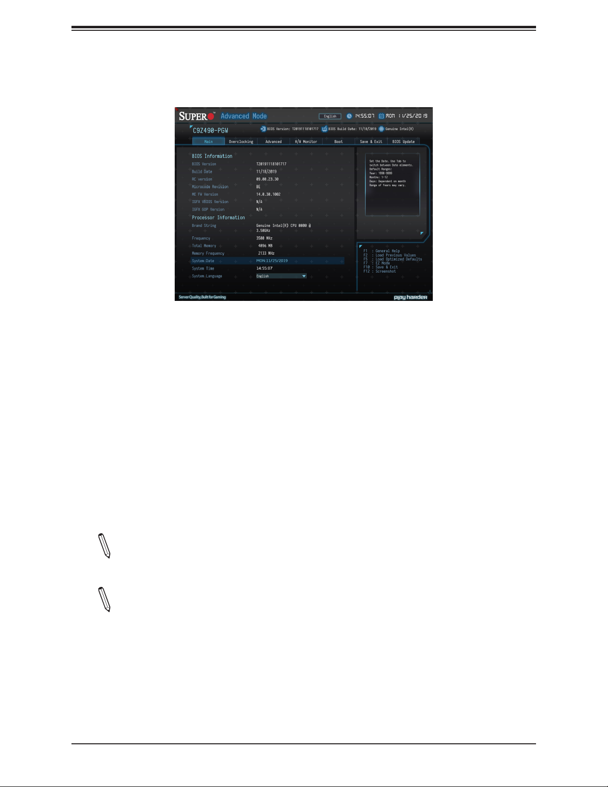
Super C9Z490-PG/-PGW User's Manual
4.3 Main
BIOS Information
The following items will be displayed:
• BIOS Version - This feature displays the version of the BIOS ROM used in the system.
• Build Date - This feature displays the date of when the BIOS ROM version used in the
system was built.
• RC Vserion - This feature displays the memory RC version.
• Microcode Revision - This feature displays the CPU's microcode patch version.
• ME FW Version - This feature displays the ME Firmware Version.
• IGFX VBIOS Version - This feature displays the Integrated Graphics VBIOS version.
Note: Invisible if the installed CPU doesn't support graphic function.
• IGFX GOP Version - This feature displays the Integrated Graphics GOP version.
Note: Invisible if the installed CPU doesn't support graphic function.
68
Page 69

Chapter 4: UEFI BIOS
Processor Information
The following items will be displayed:
• Brand String - This feature displays the brand, model name, model number of the CPU,
and its rated clock speed.
• Frequency - This feature displays the detected CPU speed
• Total Memory - This feature displays the total size of memory available in the system.
• Memory Frequency - This feature displays the detected memory speed.
System Date/System Time
Use this feature to change the system date and time. Highlight System Date or System
Time using the arrow keys. Enter new values using the keyboard. Press the <Tab> key or
the arrow keys to move between elds. The date must be entered in MM/DD/YYYY format.
The time is entered in HH:MM:SS format.
Note: The time is in the 24-hour format. For example, 5:30 P.M. appears as 17:30:00.
The date's default value is the BIOS build date after RTC reset.
System Language
Use this feature to set the system language. The options are English, 中文(繁體), 中文(简
体), 日本語, and 한국어.
69
Page 70

Super C9Z490-PG/-PGW User's Manual
4.4 Overclocking
CPU Prole
This feature allows for preset CPU overclocking proles to be selected. The options are
Stable, Default, and Performance.
BCLK Clock Frequency (1/100MHz)
Enter a value for the BCLK frequency. The default is Auto.
CPU Core Ratio
This feature determines the core ratio of CPU. The options are Auto, Sync All Cores, and
Pre Core.
*If this feature of CPU Core Ratio is set to Sync All Cores, the following feature will
become available for conguration:
Core Ratio Limit0 Override
Enter a value to apply for all cores. The default is Auto.
*If this feature of CPU Core Ratio is set to Pre Core, the following feature will become
available for conguration:
Core Ratio Limit0~X Override
Set a value for each core individually. The default is Auto.
Note: The number of X is depending on the CPU installed on the motherboard.
70
Page 71

Chapter 4: UEFI BIOS
Advanced CPU OC Setting
Processor
BCLK Aware Adaptive Voltage
This feature enables BCLK Aware Adaptive Voltage, which helps avoid high voltage
overrides by forcing pcode to be aware of the BCLK frequency when making calculations.
The options are Disabled and Enabled.
Core Max OC Ratio
This feature controls the general maximum overclocking ratio for the CPU cores and Ring.
The default is 43.
AVX2 Ratio Oset
Enter a numeric value for AVX Ratio Oset. The default is 0.
TjMax Oset
Enter a numeric value to change the Tj-Max value. The default is 0.
Cong TDP Congurations
Cong TDP Congurations
Congurable TDP Boot Mode
This feature sets the TDP Boot Mode to either Nominal, Down, OR Deactivated. When
deactivated, it will set MSR to Nominal and MMIO to zero.
Congurable TDP Lock
This feature sets the lock bits on TURBO_ACTIVATION_RATIO and CONFIG_TDP_
CONTROL. When CTDP lock is enabled, Custom Cong TDP Count will be forced to 1
and Custom Cong TDP Boot Index will be forced to 0. The options are Disabled and
Enabled.
CTDP BIOS Control
This feature enables CTDP control via runtime ACPI BIOS methods. The options are
Enabled and Disabled.
CongTDP Levels
This feature displays the level of CongTDP.
CongTDP Turbo Activation Ratio
This feature displays the value of CongTDP Turbo Activation Ratio.
71
Page 72

Super C9Z490-PG/-PGW User's Manual
Power Limit 1
This feature displays the value of Power Limit 1.
Power Limit 2
This feature displays the value of Power Limit 2.
Custom Settings Nominal
CongTDP Nominal
This feature displays the value of CongTDP Nominal.
Power Limit 1
Use this feature to set the power limit 1, in milliwatts. When the limit is exceeded, the
CPU ratio is lowered after a period of time (refer to Power Limit 1 Time Window below).
A lower limit can save power and protect the CPU, while a higher limit improves performance. This value must be between Min Power Limit TDP limit. Use the number keys
on your keyboard to enter the value. The default setting is 0.
Power Limit 2
Use this feature to set the power limit 2. Use the number keys on your keyboard to enter
the value. The default setting is 0.
Power Limit 1 Time Window
This feature determines how long the time window over which the TDP value is maintained. Use the number keys on your keyboard to enter the value. The default setting is
0. This value may vary between 0~128.
CongTDP Turbo Activation Ratio
Use this feature to set the custom value for Turbo Activation Ratio. The default setting
is 0. This value should be congured from LFM to Max Turbo.
Custom Settings Down
CongTDP Levels
This feature displays the level of CongTDP.
Power Limit 1
Use this feature to set the power limit 1, in milliwatts. When the limit is exceeded, the
CPU ratio is lowered after a period of time (refer to Power Limit 1 Time Window below).
A lower limit can save power and protect the CPU, while a higher limit improves performance. This value must be between Min Power Limit TDP limit. Use the number keys
on your keyboard to enter the value. The default setting is 0.
72
Page 73

Chapter 4: UEFI BIOS
Power Limit 2
Use this feature to set the power limit 2. Use the number keys on your keyboard to enter
the value. The default setting is 0.
Power Limit 1 Time Window
This feature determines how long the time window over which the TDP value is maintained. Use the number keys on your keyboard to enter the value. The default setting is
0. This value may vary between 0~128.
CongTDP Turbo Activation Ratio
Use this feature to set the custom value for Turbo Activation Ratio. The default setting
is 0. This value should be congured from LFM to Max Turbo.
Thermal Voltage Boost (TVB)
TVB Ratio Clipping
This feature enables CPU core frequency reduction for processors that implement Intel
Thermal Velocity Boost (TVB). For overclocking, this feature must be Disabled.
TVB Voltage Optimizations
This feature enables thermal base voltage optimizations for processors that implement
Intel Thermal Velocity Boost (TVB). The options are Disabled and Enabled.
CPU feature
CPU Feature
Hyper-Threading
This feature enables hyper-threading, which is a software method to control logical
processor threads. The options are Disabled and Enabled.
Pre-core HT Disable
Denes the per-core HT disable. Use the number keys on your keyboard to enter the
value. The default setting is 0.
Boot Performance Mode
This feature controls the performance state that the BIOS will set initially. The options
are Max Non-Turbo Performance and Turbo Performance.
73
Page 74

Super C9Z490-PG/-PGW User's Manual
Intel(R) SpeedStep(tm)
Intel SpeedStep Technology allows the system to automatically adjust processor volt-
age and core frequency in an eort to reduce power consumption and heat dissipation.
Please refer to Intel’s website for detailed information. The options are Disabled
and Enabled.
Race To Halt (RTH)
This feature enables Race To Halt, which dynamically increases CPU frequency in
order to enter package C-State faster. This will reduce overall power consumption.
The options are Disabled and Enabled.
Intel(R) Speed Shift Technology
This feature enables Intel Speed Shift, which allows the operating system to hand
control of CPU frequency and voltage to the processor. This increases P-state change
speed and improves power eciency. The options are Disabled and Enabled.
C States
C-State architecture, a processor power management platform developed by Intel,
can further reduce power consumption from the basic C1 (Halt State) state that blocks
clock cycles to the CPU. Select Enabled for CPU C-State support. The options are
Disabled and Enabled.
Thermal Monitor
This feature enables the CPU thermal monitor. The options are Disabled and Enabled.
Energy Ecient Turbo
Select Enabled to activate Energy Ecient Turbo. This feature will opportunistically
lower the turbo frequency to increase eciency. We recommend to leave this enabled
and disable only in overclock-ing situations where the turbo frequency must remain
constant. The options are Auto, Enabled, and Disabled.
Ring
Ring
Ring Max OC Ratio
Enter a numeric value for the maximum overclock ratio for CPU Ring. The default
is Auto.
Ring Down Bin
This feature enables Ring Down Bin. If set to Enabled, the maximum ring ratio will
not be observed. The options are Disabled and Enabled.
74
Page 75

Chapter 4: UEFI BIOS
Min Ring Ratio Limit
Enter a numeric value for the minimum ratio limit for CPU Ring. The default is Auto.
Max Ring Ratio Limit
Enter a numeric value for the maximum ratio limit for CPU Ring. The default is Auto.
CPU VR Settings
CPU VR Settings
VR Power Delivery Design
This feature is intended for motherboard validation purposes. The species the CFL-
S board design for VR settings override values. The default is Auto.
PSYS Slope
Enter a numeric value for the PSYS Slope. The range is 0-200. The default is 0.
PSYS Oset
Enter a numeric value for the PSYS Oset. The range is 0-255. The default is 0.
PSYS PMax Power
Enter a numeric value for the PSYS PMax Power. The range is 0-8192. The default
is 0
Acoustic Noise Settings
Acoustic Noise Settings
Acoustic Noise Mitigation
This feature enables Acoustic Noise Mitigation, which mitigates acoustic noise on
certain CPUs when they are in deep C-states.
*If the feature above is set to Enabled, the following features will become
available for conguration:
Pre Wake Time / Ramp Up Time / Ramp Down Time
Enter a numeric value for the desired feature. The range is 0-255. The default is 0.
75
Page 76

Super C9Z490-PG/-PGW User's Manual
IA VR Domain / GT VR Domain / SA VR Domain / VccIn VR Domain
Disable Fast PKG C State Ramp for IA Domain
This feature disables fast package C-state ramping in a specic domain. If set to
FALSE, the selected domain will continue to fast ramp. If set to TRUE, the selected
domain will disable fast ramping. The options are TRUE and FALSE.
Slow slew Rate for IA Domain
This feature controls the slow slew rate for a specic domain. The options are
Fast/2, Fast/4, Fast/8, and Fast/16.
Core/IA VR Settings
Core/IA VR Domain
VR Cong Enable
This feature enables VR Cong. The options are Disabled and Enabled.
AC Loading
Enter a numeric value for AC Loadline. The default is 0.
DC Loadline
Enter a numeric value for DC Loadline. The default is 0.
PS Current Threshold1
Enter a value for PS Current Threshold1. The range is 0-512. The default is 80.
PS Current Threshold2
Enter a value for PS Current Threshold2. The range is 0-512. The default is 20.
PS Current Threshold3
Enter a value for PS Current Threshold3. The range is 0-512. The default is 4.
PS3 Enable
This feature enables PS3. The options are Disabled and Enabled.
PS4 Enable
This feature enables PS4. The options are Disabled and Enabled.
IMON Slope
Enter a value for IMON Slope. The range is 0-200. The default is 0.
76
Page 77

Chapter 4: UEFI BIOS
IMON Oset
Enter a value for IMON Oset. The range is 0-63999. The default is 0.
IMON Prex
Use this feature to set the prex value as a positive (+) or a negative (-). The
options are “+” and “-”.
VR Current Limit
Enter a value for the voltage regulator current limit, with each whole number equating to 1/4A (i.e., 400 = 100A). Enter 0 for Auto.
VR Voltage Limit
Enter a value (in mV) for the voltage regulator voltage limit. The range is 0-7999.
Enter 0 for Auto.
TDC Enable
This feature enables TDC. The options are Disabled and Enabled.
TDC Current Limit
Enter a value for the TDC Current Limit, with each whole number equating to 1/8A
(i.e., 1000 = 125A). The range is 0-32767. The default is 1056.
TDC Time Windows
This feature controls the TDC Time Window. The options are 1 ms, 2 ms, 3 ms,
4 ms, 5 ms, 6 ms, 7 ms, 8 ms, and 10 ms.
TDC Lock
This feature enables TDC Lock. The options are Disabled and Enabled.
GT VR Settings
GT Domain
VR Cong Enable
This feature enables VR Cong. The options are Disabled and Enabled.
AC Loading
Enter a numeric value for AC Loadline. The default is 0.
DC Loadline
Enter a numeric value for DC Loadline. The default is 0.
77
Page 78

Super C9Z490-PG/-PGW User's Manual
PS Current Threshold1
Enter a value for PS Current Threshold1. The range is 0-512. The default is 80.
PS Current Threshold2
Enter a value for PS Current Threshold2. The range is 0-512. The default is 20.
PS Current Threshold3
Enter a value for PS Current Threshold3. The range is 0-512. The default is 4.
PS3 Enable
This feature enables PS3. The options are Disabled and Enabled.
PS4 Enable
This feature enables PS4. The options are Disabled and Enabled.
IMON Slope
Enter a value for IMON Slope. The range is 0-200. The default is 0.
IMON Oset
Enter a value for IMON Oset. The range is 0-63999. The default is 0.
IMON Prex
Use this feature to set the prex value as a positive (+) or a negative (-). The
options are “+” and “-”.
VR Current Limit
Enter a value for the voltage regulator current limit, with each whole number equating to 1/4A (i.e., 400 = 100A). Enter 0 for Auto.
VR Voltage Limit
Enter a value (in mV) for the voltage regulator voltage limit. The range is 0-7999.
Enter 0 for Auto.
Intersil VR Command
This feature enables Intersil VR Command to x VR C-state issues. The options are
Disabled, Send for IA/GT rails, and Send for IA/GT/SA rails.
78
Page 79

Chapter 4: UEFI BIOS
Thermal Voltage Boost (TVB)
TVB Ratio Clipping
This feature enables CPU core frequency reduction for processors that implement Intel
Thermal Velocity Boost (TVB). For overclocking, this feature must be Disabled.
TVB Voltage Optimizations
This feature enables thermal base voltage optimizations for processors that implement Intel
Thermal Velocity Boost (TVB). The options are Disabled and Enabled.
CPU feature
CPU Feature
Hyper-Threading
This feature enables hyper-threading, which is a software method to control logical processor threads. The options are Disabled and Enabled.
Pre-core HT Disable
Denes the per-core HT disable. Use the number keys on your keyboard to enter the
value. The default setting is 0.
Boot Performance Mode
This feature controls the performance state that the BIOS will set initially. The options
are Max Non-Turbo Performance and Turbo Performance.
Intel(R) SpeedStep(tm)
Intel SpeedStep Technology allows the system to automatically adjust processor volt-
age and core frequency in an eort to reduce power consumption and heat dissipation.
Please refer to Intel’s website for detailed information. The options are Disabled and
Enabled.
Race To Halt (RTH)
This feature enables Race To Halt, which dynamically increases CPU frequency in order
to enter package C-State faster. This will reduce overall power consumption. The options
are Disabled and Enabled.
Intel(R) Speed Shift Technology
This feature enables Intel Speed Shift, which allows the operating system to hand control
of CPU frequency and voltage to the processor. This increases P-state change speed
and improves power eciency. The options are Disabled and Enabled.
79
Page 80

Super C9Z490-PG/-PGW User's Manual
Intel(R) Turbo Boost Max Technology 3.0
Select Enabled to use the Intel Turbo Boost Max Technology. The options are Disabled
and Enabled.
C States
C-State architecture, a processor power management platform developed by Intel, can
further reduce power consumption from the basic C1 (Halt State) state that blocks clock
cycles to the CPU. Select Enabled for CPU C-State support. The options are Disabled
and Enabled.
Thermal Monitor
This feature enables the CPU thermal monitor. The options are Disabled and Enabled.
Energy Ecient Turbo
Select Enabled to activate Energy Ecient Turbo. This feature will opportunistically lower
the turbo frequency to increase eciency. We recommend to leave this enabled and dis-
able only in overclock-ing situations where the turbo frequency must remain constant.
The options are Auto, Enabled and Disabled.
Turbo Mode
Select Enabled to use the Turbo Mode to boost system performance. The options are
Disabled and Enabled.
Note: Requires to enable the feature of Intel SpeedStep or Intel Speed Shift Tech-
nology.
Ring
Ring
Ring Max OC Ratio
Enter a numeric value for the maximum overclock ratio for CPU Ring. The default is
Auto.
Ring Down Bin
This feature enables Ring Down Bin. If set to Enabled, the maximum ring ratio will not
be observed. The options are Disabled and Enabled.
Min Ring Ratio Limit
Enter a numeric value for the minimum ratio limit for CPU Ring. The default is Auto.
80
Page 81

Chapter 4: UEFI BIOS
Max Ring Ratio Limit
Enter a numeric value for the maximum ratio limit for CPU Ring. The default is Auto.
CPU VR Settings
CPU VR Settings
VR Power Delivery Design
This feature is intended for motherboard validation purposes. The species the CFL-S
board design for VR settings override values. The default is Auto.
PSYS Slope
Enter a numeric value for the PSYS Slope. The range is 0-200. The default is 0.
PSYS Oset
Enter a numeric value for the PSYS Oset. The range is 0-255. The default is 0.
PSYS PMax Power
Enter a numeric value for the PSYS PMax Power. The range is 0-8192. The default is 0.
Acoustic Noise Settings
Acoustic Noise Settings
Acoustic Noise Mitigation
This feature enables Acoustic Noise Mitigation, which mitigates acoustic noise on
certain CPUs when they are in deep C-states.
*If the feature of Acoustic Noise Mitigation is set to Enable, the following fea-
tures will become available for conguration:
Pre Wake Time / Ramp Up Time / Ramp Down Time
Enter a numeric value for the desired feature. The range is 0-255. The default is 0.
IA VR Domain / GT VR Domain / SA VR Domain / VccIn VR Domain
Disable Fast PKG C State Ramp for IA Domain
This feature disables fast package C-state ramping in a specic domain. If set to
FALSE, the selected domain will continue to fast ramp. If set to TRUE, the selected
domain will disable fast ramping. The options are TRUE and FALSE.
81
Page 82

Super C9Z490-PG/-PGW User's Manual
Slow slew Rate for IA Domain
This feature controls the slow slew rate for a specic domain. The options are Fast/2,
Fast/4, Fast/8, and Fast/16.
Core/IA VR Settings
Core/IA VR Settings
VR Cong Enable
This feature enables VR Cong. The options are Disabled and Enabled.
AC Loading
Enter a numeric value for AC Loadline. The default is 0.
DC Loadline
Enter a numeric value for DC Loadline. The default is 0.
PS Current Threshold1
Enter a value for PS Current Threshold1. The range is 0-512. The default is 80.
PS Current Threshold2
Enter a value for PS Current Threshold2. The range is 0-512. The default is 20.
PS Current Threshold3
Enter a value for PS Current Threshold3. The range is 0-512. The default is 4.
PS3 Enable
This feature enables PS3. The options are Disabled and Enabled.
PS4 Enable
This feature enables PS4. The options are Disabled and Enabled.
IMON Slope
Enter a value for IMON Slope. The range is 0-200. The default is 0.
IMON Oset
Enter a value for IMON Oset. The range is 0-63999. The default is 0.
IMON Prex
Use this feature to set the prex value as a positive (+) or a negative (-). The options are “+” and “-”.
82
Page 83

Chapter 4: UEFI BIOS
VR Current Limit
Enter a value for the voltage regulator current limit, with each whole number equating to 1/4A (i.e., 400 = 100A). Enter 0 for Auto.
VR Voltage Limit
Enter a value (in mV) for the voltage regulator voltage limit. The range is 0-7999.
Enter 0 for Auto.
TDC Enable
This feature enables TDC. The options are Disabled and Enabled.
TDC Current Limit
Enter a value for the TDC Current Limit, with each whole number equating to 1/8A
(i.e., 1000 = 125A). The range is 0-32767. The default is 1056.
TDC Time Windows
This feature controls the TDC Time Window. The options are 1 ms, 2 ms, 3 ms, 4
ms, 5 ms, 6 ms, 7 ms, 8 ms, and 10 ms.
TDC Lock
This feature enables TDC Lock. The options are Disabled and Enabled.
GT VR Settings
GT Domain
VR Cong Enable
This feature enables VR Cong. The options are Disabled and Enabled.
AC Loading
Enter a numeric value for AC Loadline. The default is 0.
DC Loadline
Enter a numeric value for DC Loadline. The default is 0.
PS Current Threshold1
Enter a value for PS Current Threshold1. The range is 0-512. The default is 80.
PS Current Threshold2
Enter a value for PS Current Threshold2. The range is 0-512. The default is 20.
83
Page 84

Super C9Z490-PG/-PGW User's Manual
PS Current Threshold3
Enter a value for PS Current Threshold3. The range is 0-512. The default is 4.
PS3 Enable
This feature enables PS3. The options are Disabled and Enabled.
PS4 Enable
This feature enables PS4. The options are Disabled and Enabled.
IMON Slope
Enter a value for IMON Slope. The range is 0-200. The default is 0.
IMON Oset
Enter a value for IMON Oset. The range is 0-63999. The default is 0.
IMON Prex
Use this feature to set the prex value as a positive (+) or a negative (-). The options are “+” and “-”.
VR Current Limit
Enter a value for the voltage regulator current limit, with each whole number equating to 1/4A (i.e., 400 = 100A). Enter 0 for Auto.
VR Voltage Limit
Enter a value (in mV) for the voltage regulator voltage limit. The range is 0-7999.
Enter 0 for Auto.
TDC Enable
This feature enables TDC. The options are Disabled and Enabled.
TDC Current Limit
Enter a value for the TDC Current Limit, with each whole number equating to 1/8A
(i.e., 1000 = 125A). The range is 0-32767. The default is 1056.
TDC Time Windows
This feature controls the TDC Time Window. The options are 1 ms, 2 ms, 3 ms, 4
ms, 5 ms, 6 ms, 7 ms, 8 ms, and 10 ms.
TDC Lock
This feature enables TDC Lock. The options are Disabled and Enabled.
84
Page 85

Chapter 4: UEFI BIOS
Intersil VR Command
This feature enables Intersil VR Command to x VR C-state issues. The options are
Disabled, Send for IA/GT rails, and Send for IA/GT/SA rails.
GT
GT Domain
GT OverClocking Frequency
Enter a value for the overclocked RP0 frequency (in multiples of 50 MHz) in the GT
domain. The default is 0.
GT Voltage Mode
This feature controls the voltage mode in the GT domain. The options are Adaptive
and Override.
GT Extra Turbo Voltage
Enter a value for the extra turbo voltage (in mV) that will be applied while GT is operating in turbo mode. The default is 0.
GT Voltage Oset
Enter a value for the oset voltage (in mV) that will be applied to the GT domain. The
default is 0.
Oset Prex
Use this feature to set the prex value as a positive (+) or a negative (-). The options
are “+” and “-”.
GT Unslice Domain
GT OverClocking Frequency
Enter a value for the overclocked RP0 frequency (in multiples of 50 MHz) in the GT
Unslice domain. The default is 0.
GT Voltage Mode
This feature controls the voltage mode in the GT Unslice domain. The options are
Adaptive and Override.
GT Extra Turbo Voltage
Enter a value for the extra turbo voltage (in mV) that will be applied while GT is operating in turbo mode. The default is 0.
85
Page 86

Super C9Z490-PG/-PGW User's Manual
GTU Voltage Oset
Enter a value for the oset voltage (in mV) that will be applied to the GT domain. The
default is 0.
Oset Prex
Use this feature to set the prex value as a positive (+) or a negative (-). The options
are “+” and “-”.
Memory Prole
This feature controls the memory prole. The options are Default prole and Custom prole.
*If this feature above is set to "Custom prole", the following memory congurations
become available:
Memory Reference Clock
This feature controls the memory reference clock, in MHz. The options are 133 and 100.
QCLK Odd Ratio
If set to Enabled, this feature adds the Memory Reference Clock amount to the QCLK
frequency. The options are Disabled and Enabled.
Memory Frequency
Use this feature to set the frequency of the memory installed. The options are Auto,
DDR4-1067MHz, DDR4-1333MHz, DDR4-1600MHz, DDR4-1867MHz, DDR4-2133MHz,
DDR4-2400MHz, DDR4-2667MHz, DDR4-2933MHz, DDR4-3200MHz, DDR4-3467MHz,
DDR4-3733MHz, DDR4-4000Hz, DDR4-4267MHz, DDR4-4533MHz, DDR4-4800MHz,
DDR4-5067MHz, DDR4-5333MHz, DDR4-5600MHz, DDR4-5867MHz, DDR4-6133MHz,
DDR4-6400MHz, DDR4-6667MHz, DDR4-6933MHz, DDR4-7200MHz, DDR4-7467MHz,
DDR4-7733MHz, DDR4-8000MHz, and DDR4-8267MHz.
Advanced Memory OC Setting
*The features below are available when the Memory Prole is set to Custom prole.
Processor
Realtime Memory Timing
This feature enables realtime memory timing changes to be made after MRC_DONE. The
options are Disabled and Enabled.
tCL
This festure congures the Cas Latency Range. Enter a numeric value between 0-31.
The default is 15.
86
Page 87

Chapter 4: UEFI BIOS
tRCD/tRP
This feature congures the RAS to CAS delay time. Enter a numeric value between 1-63.
The default is 15.
tRAS
This feature congures the Ras Active Time. Enter a numeric value between 1-64. The
default is 36.
tCWL
This feature congures the Minimum CAS Write Latency Time. Enter a numeric value
between 1-20. The default is Auto.
tFAW
This feature congures the Minimum Four Activate Window Delay Time. Enter a numeric
value between 0-63. The default is Auto.
tREFI
This feature congures the Maximum tREFI Time (Average Periodic Refrech Interval).
Enter a numeric value between 0-65535. The default is Auto.
tRFC
This feature congures the Minimum Refrech Recovery Delay Time. Enter a numeric
value between 0-1023. The default is Auto.
tRRD
This feature congures the Minimum Row Active to Row Active Delay Time. Enter a
numeric value between 0-31. The default is Auto.
tRTP
This feature congures the Minimum Internal Read to Precharge Command Delay Time.
The default is Auto.
tCCD_L
Enter a numeric value for desired tCCD_L. The default is Auto.
tWR
This festure congures the Minimum Write Recovery Time. The options are Auto, 5, 6,
7, 8, 10, 12, 14, 16, 18, 20, 22, 24, 26, 28, 30, 32, 34, 36, 38, 40, 42 and 44.
tWTR
This feature congures the Minimum Internal Write to Read Command Delay Time. Enter
a numeric value between 0-28. The default is Auto.
87
Page 88

Super C9Z490-PG/-PGW User's Manual
NMode
This feature congures the System Command Rate. Enter a numeric value between 0-2.
The default is Auto.
tRRD_sg
tRRD_dg
tRDRD_sg
tRDRD_dg
tRDRD_dr
tRDRD_dd
tRDWR_sg
tRDWR_dg
tRDWR_dr
tRDWR_dd
tWRRD_sg
tWRRD_dg
tWRRD_dr
tWRRD_dd
tWRWR_sg
tWRWR_dg
tWRWR_dr
tWRWR_dd
tCKE
ODT RTT WR
ODT RTT PARK
ODT RTT NOM
SCompDq StageDelayPS
SCompCmd StageDelayPS
SCompCtl StageDelayPS
SCompClk StageDealyPS
88
Page 89

Chapter 4: UEFI BIOS
RcompTarget[RdOdt]
RcompTarget[WrDS]
RcompTarget[WrDSCmd]
RcompTarget[WrDSCtl]
RcompTarget[WrDSClk]
DllBwEn[0]
DllBwEn[1]
DllBwEn[2]
DllBwEn[3]
Enter a desired numeric value above for each feature. The default of these features is 0.
Load line Calibration
This feature controls the load line calibration. The options are Disabled, Level 1, Level 2,
Level 3, Level 4, Level 5, Level 6, Level 7, and Auto.
Core Voltage Mode
This feature controls the core voltage mode. The options are Adaptive and Override.
VF Point Oset Mode
Use this feature to select Legacy or Selection mode. The options are Legacy and Selection.
*If the feature above is set to Legacy, the following features will become available for
conguration:
Core Voltage Oset
Enter a value for the oset voltage (in mV) that will be applied to the IA Core domain. The
default is Auto.
Oset Prex
Use this feature to set the prex value as a positive (+) or a negative (-). The options are
“+” and “-”.
Note: If there is any change to this setting, you will need to power o and reboot the
system for the change to take eect.
Core Extra Turbo Voltage
Enter a numeric value for the extra turbo voltage (in mV) that will be applied while IA Core
is operating in turbo mode. The default is Auto.
89
Page 90

Super C9Z490-PG/-PGW User's Manual
Memory Voltage
Enter a numeric value for the memory voltage override. The default is Auto.
PCH Voltage
Enter a numeric value for the PCH voltage override. The default is Auto.
CPU_IO Voltage
Enter a numeric value for the CPU IO voltage override. The default is Auto.
System Agent Voltage (mV)
Enter a numeric value for the System Agent voltage (in mV). The default is Auto.
Advanced Voltage OC Setting
Voltage Conguration
VPP Voltage
CPU PLL Voltage
PCH 1.8 Voltage
VCC DMI Voltage
Vcc_ST
Vcc_PLL
Enter a desired numeric value above for each feature. The default of these features is Auto.
Uncore
Uncore
Uncore Voltage Oset
Enter a value for the oset voltage (in mV) that will be applied to the Uncore domain.
The default is 0.
Uncore Voltage Oset
Use this feature to set the prex value as a positive (+) or a negative (-). The options
are “+” and “-”.
90
Page 91

Chapter 4: UEFI BIOS
Voltage PLL Trim Controls
Voltage PLL Trim Controls
Core PLL Voltage Oset
GT PLL Voltage Oset
Ring PLL Voltage Oset
System Agent PLL Voltage Oset
Memory Controller PLL Voltage Oset
Enter a desired numeric value above for each feature. The range is 0-63 and the default
is 0.
91
Page 92

Super C9Z490-PG/-PGW User's Manual
4.5 Advanced
Setup Mode
This feature sets the default mode to start in after entering BIOS. The options are EZ Mode
and Advanced Mode.
Boot Feature
Fast Boot
This feature enables the system to boot with a minimal set of required devices to launch.
This has no eect on BBS boot options. The options are Disabled and Enabled.
Quiet Boot
Use this feature to select the screen display between the POST messages and the OEM
logo upon bootup. Uncheck the box to display the POST messages. Check the box to
display the OEM logo instead of the normal POST messages. The default is Checked.
Bootup NumLock State
Use this feature to set the Power-on state for the <Numlock> key. The options are O and
On.
Wait For "F1" If Error
Use this feature to force the system to wait until the "F1" key is pressed if an error occurs.
The options are Disabled and Enabled.
92
Page 93

Chapter 4: UEFI BIOS
Re-try Boot
If this feature is enabled, the BIOS will automatically reboot the system from a specied boot
device after its initial boot failure. The options are Disabled, Legacy Boot, and EFI Boot.
Power Conguration
Watch Dog Function
If enabled, the Watch Dog Timer will allow the system to reset or generate NMI based on
jumper settings when it is expired for more than ve minutes. The options are Disabled
and Enabled.
AC Loss Policy Depend on
Use this feature to set the power state after a power outage. Select Stay O for the system
power to remain o after a power loss. Select Power On for the system power to be turned
on after a power loss. Select Last State to allow the system to resume its last power state
before a power loss. The options are Stay O, Power On, and Last State.
Power Button Function
This feature controls how the system shuts down when the power button is pressed.
Select 4 Seconds Override for the user to power o the system after pressing and holding
the power button for four seconds or longer. Select Instant O to instantly power o the
system as soon as the user presses the power button. The options are Instant O and 4
Seconds Override.
DeepSx Power Policies
This feature enables DeepSx Power Policy conguration. The options are Disabled and
Enabled in S4-S5.
Connectivity Conguration
Note:
Connectivity Conguration
The following information will be displayed:
This submenu becomes congurable when a CNVi device is plugged into the moth-
erboard. It's already built-in in C9Z490-PGW.
• CNVi present - display the status of wireless connection
CNVi Conguration
CNVi WiFi&BT
This feature enables CNVi WiFi and Bluetooth support. The options are Disabled and
Enabled.
93
Page 94

Super C9Z490-PG/-PGW User's Manual
CPU Conguration
CPU Conguration
The following CPU information will be displayed:
• Brand String - the brand and speed of installed CPU
• Frequency - the frequency of installed CPU
• ID - the unique CPU ID
• Stepping - the processor stepping
• Number of Processors - the number of cores detected / the number of threads detected
Advanced Option - enabled or disabled the advanced features
*If this feature of Advanced Option is set to Eabled, the following information will
be displayed:
• Microcode Revision
• GT Info
• IGFX VBSIO Version (Invisible if the installed CPU doesn't have integrated graphics.)
• IGFX GOP Version (Invisible if the installed CPU doesn't have integrated graphics.)
• L1 Data Cache
• L1 Instruction Cache
• L2 Cache
• L3 Cache
• VMX
• SMX/TXT
C6DRAM
This feature enables moving DRAM contents to PRM memory when the CPU is in a C6
state. The options are Disabled and Enabled.
Note: This feature is available depending on the CPU.
Software Guard Extensions (SGX)
Select Enabled to activate the Software Guard Extensions (SGX). The options are Enabled,
Disabled, and Software Controlled.
Note: This feature is available depending on the CPU.
94
Page 95

Chapter 4: UEFI BIOS
*If this feature of SGX is set to Enabled, the following features will become available
for conguration:
Select Owner EPOCH Input Type
There are three Owner EPOCH modes (each EPOCH is 64 bit). The options are No Change
in Owner EPOCHs, Change to New Random Owner EPOCH, and Manual User Dened
Owner EPOCHs.
*If this feature of Select Owner EPOCH Input Type is set to Manual User Dened
Owner EPOCHs, the following features will become available for conguration:
Software Guard Extensions Epoch 0
Enter a numeric value for this feature. The default is 0.
Software Guard Extensions Epoch 1
Enter a numeric value for this feature. The default is 0.
PRMRR Size
The BIOS must reserve a contiguous region of Processor Reserved Memory (PRM) in the
Processor Reserved Memory Range Register (PRMRR). The options are 32MB, 64MB,
and 128MB.
*If this feature of SGX is set to Software Controlled, the following feature will become
available for conguration:
Select Owner EPOCH Input Type
There are three Owner EPOCH modes (each EPOCH is 64 bit). The options are No Change
in Owner EPOCHs, Change to New Random Owner EPOCH, and Manual User Dened
Owner EPOCHs.
*If this feature of Select Owner EPOCH Input Type is set to Manual User Dened
Owner EPOCHs, the following features will become available for conguration:
Software Guard Extensions Epoch 0
Enter a numeric value for this feature. The default is 0.
Software Guard Extensions Epoch 1
Enter a numeric value for this feature. The default is 0.
95
Page 96

Super C9Z490-PG/-PGW User's Manual
Hardware Prefetcher
If set to Enabled, the hardware prefetcher will prefetch streams of data and instructions
from the main memory to the L2 cache to improve CPU performance. The options are
Disabled and Enabled.
Adjacent Cache Line Prefetch
Select Enabled for the CPU to prefetch both cache lines for 128 bytes as comprised. Select
Disabled for the CPU to prefetch both cache lines for 64 bytes. The options are Disabled
and Enabled.
Intel (VMX) Virtualization Technology
Select Enabled to use the Intel Virtualization Technology to allow one platform to run multiple
operating systems and applications in independent partitions, creating multiple "virtual"
systems in one physical computer. The options are Disabled and Enabled.
Active Processor Cores
Use this feature to select the number of active processor cores. The default option is All.
The available options depend on how many cores are supported by the CPU.
Hyper-Threading
Select Enabled to support Intel Hyper-threading Technology to enhance CPU performance.
The options are Disabled and Enabled.
BIST
Select Enabled to activate the Built-In Self Test (BIST) on reset. The options are Disabled
and Enabled.
AES
Select Enabled for Intel CPU Advanced Encryption Standard (AES) In-structions support
to enhance data integrity. The options are Disabled and Enabled.
Machine Check
Select Enabled to activate Machine Check. The options are Disabled and Enabled.
MonitorMWait
Select Enabled to activate MonitorMWait. The options are Disabled and Enabled.
Reset AUX Content
Use this feature to reset the TPM Auxiliary content. The options are Yes and No.
FCLK Frequency for Early Power On
Select the FCLK frequency for early power on. The options are Normal (800MHz), 1GHz,
400MHz, and Auto.
Note: The option of 1GHz is not supported for ULT/ULX SKUs.
96
Page 97

Chapter 4: UEFI BIOS
Graphics Conguration
Graphics Conguration
Note: Only the feature of Primary Display is available for conguring if the installed
CPU doesn’t have integrated graphics.
Graphics Turbo IMON Current
Enter a value for the graphics turbo IMON current. The range is 14-31. The default is 31.
Skip Scanning of External Gfx Card
This feature disables scanning for external graphics cards. When this feature is set to
Enabled, the system will not scan for external graphics cards on PEG and PCH PCI-E
ports. The options are Disabled and Enabled.
Primary Display
This feature controls which graphics device will be used as the primary display. The
options are Auto, IGFX, PEG, and PCI.
Internal Graphics
This item keeps the IGD (Internal Graphics Device) enabled, based on setup options. The
options are Auto, Enabled and Disabled.
GTT Size
This feature controls the memory allocation size for the graphics translation table (GTT).
The options are 2MB, 4MB, and 8MB.
Aperture Size
This feature controls the graphics aperture size. For optimal performance, select the size
that matches the installed graphics card's size. The options are 128MB, 256MB, 512MB,
1024MB, and 2048MB.
DVMT Pre-Allocated
This feature controls the DVMT 5.0 Pre-allocated graphics memory size to be used by the
internal grahics device. The options are 0M, 32M, 64M, 4M, 8M, 12M, 16M, 20M, 24M,
28M, 32M/F7, 36M, 40M, 44M, 48M, 52M, 56M, and 60M.
DVMT Total Gfx Mem
This feature controls the DVMT 5.0 total graphics size to be used by the internal graphics
device. The options are 128M, 256M, and MAX.
PM Support
This feature enables PM support. The options are Disabled and Enabled.
97
Page 98

Super C9Z490-PG/-PGW User's Manual
PAVP Enable
This feature enables PAVP support. The options are Disabled and Enabled.
Cdynmax Clamping Enable
This feature enables Cdynmax Clamping. The options are Disabled and Enabled.
Graphics Clock Frequency
This feature controls the graphics clock frequency. Select the highest clock frequency
supported by the platform. The options are 337.5 Mhz, 450 Mhz, 540 Mhz, and 675 Mhz.
Skip CD Clock Init in S3 resume
This feature enables skipping the full CD clock initialization. If set to Disabled, the full CD
clock will initialize. The options are Disabled and Enabled.
HDD Security Conguration
HDD Security Conguration
HDD Password Conguration
Information for the following is displayed:
• P0
• Security Supported
• Security Enabled
• Security Locked
• Security Frozen
• HDD User Pwd Status
• HDD Master Pwd Status
Set User Password
Press <Enter> to create a new, or change an existing HDD password.
98
Page 99

Chapter 4: UEFI BIOS
HTTP BOOT Conguration
HTTP BOOT Conguration
Http Boot One Time
This feature enables HTTP Boot, which is a client-server communication based application
for system deployment and conguration over a network. The options are Disabled and
Enabled.
Input the description
Enter a name for Http boot option.
Boot URI
Enter a value for a new Boot option to be created according to this Boot URI. The default
is Null.
Memory conguration
Memory conguration
The following memory information will be displayed:
• Memory RC Version - displays the memory reference code version.
• Memory Frequency - displays the frequency of the installed memory.
• Memory Timings (tCL-tRCD-tRP-tRAS)
• DIMMA1 - displays if a DIMM is installed on this slot, and the DIMM size.
• DIMMA2 - displays if a DIMM is installed on this slot, and the DIMM size.
• DIMMB1 - displays if a DIMM is installed on this slot, and the DIMM size.
• DIMMB2 - displays if a DIMM is installed on this slot, and the DIMM size.
Maximum Memory Frequency
This feature selects the type/speed of the memory installed. The options are Auto, 1067,
1200, 1333, 1400, 1600, 1800, 1867, 2000, 2133, 2200, 2400, 2600, 2667, 2800, 2933,
3000, 3200, 3400, 3467, 3600, 3733, 3800, 4000, 4200, 4267, 4400, 4533, 4600, 4800,
5000, 5067, 5200, 5333, 5400, 5600, 5800, 5867, 6000, 6133, and 6200. All values are
in MHz.
99
Page 100

Super C9Z490-PG/-PGW User's Manual
Max TOLUD (Top of Low Usable DRAM)
This feature sets the maximum TOLUD value, which species the "Top of Low Usable
DRAM" memory space to be used by internal graphics devices, GTT Stolen Memory, and
TSEG, respectively, if these devices are enabled. The options are Dynamic, 1 GB, 1.25
GB, 1.5 GB, 1.75 GB, 2 GB, 2.25 GB, 2.5 GB, 2.75 GB, 3 GB, 3.25 GB, and 3.5 GB.
Note: TSEG is a block of memory that is only accessible by the processor while operat-
ing in System Management Mode (SMM).
Memory Scrambler
This feature enables memory scrambler support for memory error cor-rection. The options
are Disabled and Enabled.
Force ColdReset
Use this feature when ColdBoot is required during MRC execution. The options are
Disabled and Enabled.
Force Single Rank
When enabled, only Rank0 will be use in each DIMM. The options are Disabled and
Enabled.
Memory Remap
PCI memory resources will overlap with the total physical memory if 4GB of memory (or
above) is installed on the motherboard. When this occurs, Enable this function to reallocate
the overlapped physical memory to a location above the total physical memory to resolve
the memory overlap-ping situation. The options are Disabled and Enabled.
MRC Fast Boot
This feature enables or disables fast path through MRC. The options are Disabled and
Enabled.
NCT6796DE Super IO Conguration
NCT6796DE Super IO Conguration
• Super IO Chip - NCT6796DE
Serial Port 1 Conguration
Serial Port 1 Conguration
100
 Loading...