

Page 1

C9Z390-PGW
USER’S MANUAL
Revision 1.0
Page 2

!
The information in this User’s Manual has been carefully reviewed and is believed to be accurate. The
vendor assumes no responsibility for any inaccuracies that may be contained in this document, makes
no commitment to update or to keep current the information in this manual, or to notify any person
or organization of the updates. Please Note: For the most up-to-date version of this manual,
please see our web site at www.supermicro.com.
Super Micro Computer, Inc. ("Supermicro") reserves the right to make changes to the product described in this manual at any time and without notice. This product, including software and documentation, is the property of Supermicro and/or its licensors, and is supplied only under a license. Any use or
reproduction of this product is not allowed, except as expressly permitted by the terms of said license.
IN NO EVENT WILL SUPERMICRO BE LIABLE FOR DIRECT, INDIRECT, SPECIAL, INCIDENTAL, SPECULATIVE OR CONSEQUENTIAL DAMAGES ARISING FROM THE USE OR INABILITY
TO USE THIS PRODUCT OR DOCUMENTATION, EVEN IF ADVISED OF THE POSSIBILITY OF
SUCH DAMAGES. IN PARTICULAR, SUPERMICRO SHALL NOT HAVE LIABILITY FOR ANY
HARDWARE, SOFTWARE, OR DATA STORED OR USED WITH THE PRODUCT, INCLUDING THE
COSTS OF REPAIRING, REPLACING, INTEGRATING, INSTALLING OR RECOVERING SUCH
HARDWARE, SOFTWARE, OR DATA.
Any disputes arising between manufacturer and customer shall be governed by the laws of Santa
Clara County in the State of California, USA. The State of California, County of Santa Clara shall be
the exclusive venue for the resolution of any such disputes. Super Micro's total liability for all claims
will not exceed the price paid for the hardware product.
FCC Statement: This equipment has been tested and found to comply with the limits for a class B
digital device, pursuant to Part 15 of the FCC Rules. These limits are designed to provide reasonable
protection against harmful interference in a residential installation. This equipment generates, uses,
and can radiate radio frequency energy and, if not installed and used in accordance with the instructions, may cause harmful interference to radio communications. However, there is no guarantee that
interference will not occur in a particular installation. If this equipment does cause harmful interference to radio or television reception, which can be determined by turning the equipment off and on,
the user is encouraged to try to correct the interference by one or more of the following measures:
• Reorient or relocate the receiving antenna.
• Increase the separation between the equipment and receiver.
• Connect the equipment to an outlet on a circuit different from that to which the
receiver is connected.
• Consult the authorized dealer or an experienced radio/TV technician for help.
California Best Management Practices Regulations for Perchlorate Materials: This Perchlorate warning
applies only to products containing CR (Manganese Dioxide) Lithium coin cells. “Perchlorate Material-
special handling may apply. See www.dtsc.ca.gov/hazardouswaste/perchlorate”
WARNING: This product can expose you to chemicals including
lead, known to the State of California to cause cancer and birth
defects or other reproductive harm. For more information, go
to www.P65Warnings.ca.gov.
Manual Revision: 1.0
Release Date: Oct 11, 2018
Unless you request and receive written permission from Super Micro Computer, Inc., you may not
copy any part of this document.
Information in this document is subject to change without notice. Other products and companies
referred to herein are trademarks or registered trademarks of their respective companies or mark
holders.
Copyright © 2018 by Super Micro Computer, Inc. All rights reserved.
Printed in the United States of America
Page 3

Preface
Preface
This manual is written for system integrators, PC technicians and
knowledgeable PC users. It provides information for the installation and
use of the C9Z390-PGW motherboard.
Manual Organization
Chapter 1 describes the features, specications and performance of
the motherboard, and provides detailed information on the Intel Z390
chipset.
Chapter 2 provides hardware installation instructions. Read this chapter when installing the processor, memory modules and other hardware
components into the system.
If you encounter any problems, see Chapter 3, which describes troubleshooting procedures for video, memory and system setup stored in the
CMOS.
Chapter 4 includes an introduction to the BIOS, and provides detailed
information on running the CMOS Setup utility.
Appendix A provides BIOS Error Beep Codes.
Appendix B lists software program installation instructions.
Appendix C contains UEFI BIOS Recovery instructions.
iii
Page 4

Supermicro C9Z390-PGW Motherboard User’s Manual
Checklist
Congratulations on purchasing your computer motherboard from an acknowledged leader in the industry. Supermicro boards are designed with
the utmost attention to detail to provide you with the highest standards
in quality and performance.
Please check that the following items have all been included with your
motherboard. If anything listed here is damaged or missing, contact
your retailer.
The following items are included in the retail box:
• One (1) Supermicro Motherboard
• Four (4) SATA cables
• One (1) I/O shield
• One (1) Quick Reference Guide
• One (1) Driver CD
• Two (2) Antennas
Conventions Used in the Manual
Special attention should be given to the following symbols for proper
installation and to prevent damage done to the components or injury
to yourself:
Attention! Critical information to prevent damage to the components or injury to yourself.
Important: Important information given to ensure proper system installation or to relay safety precautions.
Note: Additional Information given to differentiate various models or provides information for correct system setup.
iv
Page 5

Standardized Warning Statements
Standardized Warning Statements
The following statements are industry-standard warnings, provided to
warn the user of situations which have the potential for bodily injury.
Should you have questions or experience difculty, contact Supermicro's
Technical Support department for assistance. Only certied technicians
should attempt to install or congure components.
Read this section in its entirety before installing or conguring compo-
nents in the Supermicro chassis.
Battery Handling
Warning!
There is a danger of explosion if the battery is replaced incorrectly. Replace the battery only with the same or equivalent type recommended
by the manufacturer. Dispose of used batteries according to the manufacturer's instructions
電池の取り扱い
電池交換が正しく行われなかった場合、破裂の危険性があります。 交換する電池はメー
カーが推奨する型、または同等のものを使用下さい。 使用済電池は製造元の指示に従
って処分して下さい。
警告
电池更换不当会有爆炸危险。请只使用同类电池或制造商推荐的功能相当的电池更
换原有电池。请按制造商的说明处理废旧电池。
警告
電池更換不當會有爆炸危險。請使用製造商建議之相同或功能相當的電池更換原有
電池。請按照製造商的說明指示處理廢棄舊電池。
Warnung
Bei Einsetzen einer falschen Batterie besteht Explosionsgefahr. Ersetzen
Sie die Batterie nur durch den gleichen oder vom Hersteller empfohlenen
Batterietyp. Entsorgen Sie die benutzten Batterien nach den Anweisungen
des Herstellers.
Attention
Danger d'explosion si la pile n'est pas remplacée correctement. Ne la
remplacer que par une pile de type semblable ou équivalent, recom-
mandée par le fabricant. Jeter les piles usagées conformément aux
instructions du fabricant.
v
Page 6

Supermicro C9Z390-PGW Motherboard User’s Manual
¡Advertencia!
Existe peligro de explosión si la batería se reemplaza de manera incorrecta. Reemplazar la batería exclusivamente con el mismo tipo o el
equivalente recomendado por el fabricante. Desechar las baterías gastadas según las instrucciones del fabricante.
!הרהזא
תנכס תמייקץוציפ .הניקת אל ךרדב הפלחוהו הדימב הללוסה לש ףילחהל שי
גוסב הללוסה תא מ םאותה תרבחלמומ ןרציתצ.
תוללוסה קוליס תושמושמה עצבל שי .ןרציה תוארוה יפל
경고!
배터리가 올바르게 교체되지 않으면 폭발의 위험이 있습니다. 기존 배터리와 동일
하거나 제조사에서 권장하는 동등한 종류의 배터리로만 교체해야 합니다. 제조사
의 안내에 따라 사용된 배터리를 처리하여 주십시오.
Waarschuwing
Er is ontplofngsgevaar indien de batterij verkeerd vervangen wordt. Vervang de batterij slechts met hetzelfde of een equivalent type die door de
fabrikant aanbevolen wordt. Gebruikte batterijen dienen overeenkomstig
fabrieksvoorschriften afgevoerd te worden.
Product Disposal
Warning!
Ultimate disposal of this product should be handled according to all national laws and regulations.
vi
Page 7

Standardized Warning Statements
製品の廃棄
この製品を廃棄処分する場合、国の関係する全ての法律・条例に従い処理する必要が
ありま す。
警告
本产品的废弃处理应根据所有国家的法律和规章进行。
警告
本產品的廢棄處理應根據所有國家的法律和規章進行。
Warnung
Die Entsorgung dieses Produkts sollte gemäß allen Bestimmungen und
Gesetzen des Landes erfolgen.
¡Advertencia!
Al deshacerse por completo de este producto debe seguir todas las leyes
y reglamentos nacionales.
Attention
La mise au rebut ou le recyclage de ce produit sont généralement soumis
à des lois et/ou directives de respect de l'environnement. Renseignezvous auprès de l'organisme compétent.
רצומה קוליס
!הרהזא
ו תויחנהל םאתהב תויהל בייח הז רצומ לש יפוס קוליס.הנידמה יקוח
경고!
이 제품은 해당 국가의 관련 법규 및 규정에 따라 폐기되어야 합니다.
Waarschuwing
De uiteindelijke verwijdering van dit product dient te geschieden in over-
eenstemming met alle nationale wetten en reglementen.
vii
Page 8

Supermicro C9Z390-PGW Motherboard User’s Manual
Contacting Supermicro
Headquarters
Address: Super Micro Computer, Inc.
980 Rock Ave.
San Jose, CA 95131 U.S.A.
Tel: +1 (408) 503-8000
Fax: +1 (408) 503-8008
Email: marketing@supermicro.com (General Information)
support@supermicro.com (Technical Support)
Website: www.supermicro.com
Europe
Address: Super Micro Computer B.V.
Het Sterrenbeeld 28, 5215 ML
's-Hertogenbosch, The Netherlands
Tel: +31 (0) 73-6400390
Fax: +31 (0) 73-6416525
Email: sales@supermicro.nl (General Information)
support@supermicro.nl (Technical Support)
rma@supermicro.nl (Customer Support)
Website: www.supermicro.nl
Asia-Pacic
Address: Super Micro Computer, Inc.
3F, No. 150, Jian 1st Rd.
Zhonghe Dist., New Taipei City 235
Taiwan (R.O.C)
Tel: +886-(2) 8226-3990
Fax: +886-(2) 8226-3992
Email: support@supermicro.com.tw
Website: www.supermicro.com.tw
viii
Page 9

Contacting Supermicro
Where to Find More Information
For your system to work properly, please follow the links below to
download all necessary drivers/utilities and the user's manual for your
motherboard.
Supermicro product manuals: http://www.supermicro.com/support/
manuals/
Product Drivers and utilities: https://www.supermicro.com/wftp/driver/
If you have any questions, please contact our support team at support@
supermicro.com.
ix
Page 10

Supermicro C9Z390-PGW Motherboard User’s Manual
Table of Contents
Preface
Chapter 1 Introduction
1-1 Overview .............................................................................. 1-1
About this Motherboard .......................................................... 1-1
1-2 Chipset Overview .................................................................. 1-1
Intel Z390 Chipset Features .................................................... 1-1
1-3 Motherboard Features ............................................................... 1-2
1-4 Special Features .................................................................... 1-4
Recovery from AC Power Loss ................................................. 1-4
1-5 PC Health Monitoring .............................................................. 1-4
Fan Status Monitor with Firmware Control ............................... 1-4
Environmental Temperature Control ......................................... 1-4
System Resource Alert ........................................................... 1-5
1-6 ACPI Features ....................................................................... 1-5
Slow Blinking LED for Suspend-State Indicator .......................... 1-5
1-7 Power Supply ........................................................................ 1-6
1-8 Super I/O ............................................................................. 1-6
Chapter 2 Installation
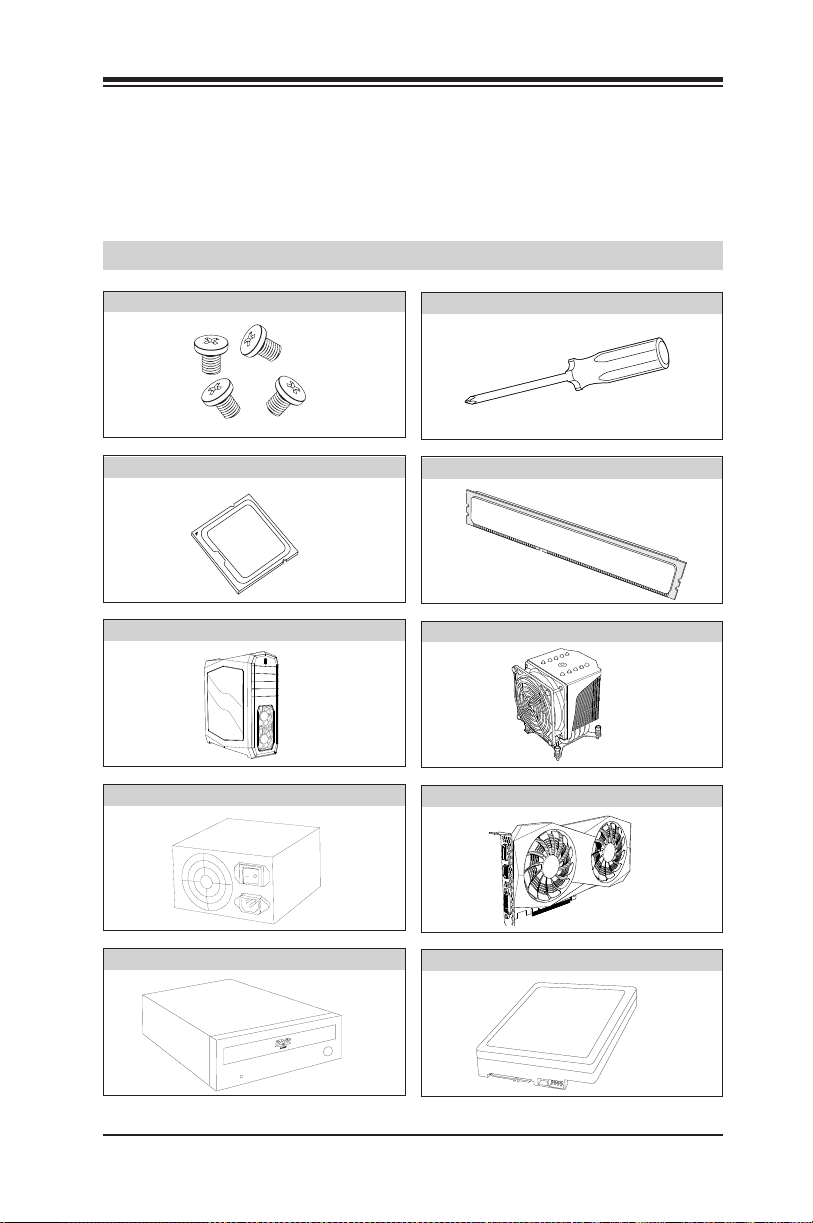
2-1 Installation Components and Tools Needed ............................... 2-1
2-2 Static-Sensitive Devices .......................................................... 2-2
Precautions ........................................................................... 2-2
Unpacking ............................................................................. 2-2
2-3 Processor and Heatsink Installation .......................................... 2-3
Installing the LGA1151 Processor ........................................... 2-3
Installing an Active CPU Heatsink with Fan ............................... 2-6
Removing an Active CPU Heatsink with Fan ............................... 2-7
2-4 Installing DDR4 Memory ......................................................... 2-8
DIMM Installation .................................................................. 2-8
Removing Memory Modules ..................................................... 2-8
Memory Support .................................................................... 2-9
Memory Population Guidelines ............................................... 2-10
2-4 M.2 Installation (optional) ..................................................... 2-11
2-5 Motherboard Installation ....................................................... 2-12
Tools Needed ....................................................................... 2-12
Location of Mounting Holes ................................................... 2-12
Installing the Motherboard .................................................... 2-13
x
Page 11

Table of Contents
2-6 Connectors/IO Ports ............................................................. 2-14
Back I/O Panel .................................................................... 2-14
Universal Serial Bus (USB) ................................................ 2-15
Back Panel High Denition Audio (HD Audio) ...................... 2-17
ATX PS/2 Keyboard/Mouse Ports ........................................ 2-18
VESA® DisplayPort™ ........................................................ 2-18
HDMI Port ....................................................................... 2-18
Ethernet Port ................................................................... 2-18
Front Control Panel .............................................................. 2-19
Front Control Panel Pin Denitions ......................................... 2-20
Power LED ..................................................................... 2-20
HDD LED ........................................................................ 2-20
NIC1 (LAN) ..................................................................... 2-20
Reset Button .................................................................. 2-21
Power Button .................................................................. 2-21
Overheat (OH)/Fan Fail ..................................................... 2-21
2-7 Connecting Cables ............................................................... 2-22
ATX Main PWR & CPU PWR Connectors (JPW1 & JPW2) ........ 2-22
Fan Headers (Fan1-5) ....................................................... 2-23
Chassis Intrusion (JL1) .................................................... 2-23
Speaker (JD1) ................................................................. 2-24
Onboard Power LED (JLED1) .............................................. 2-25
Serial Port (COM1) ........................................................... 2-25
DOM PWR Connector (JSD1).............................................. 2-26
Standby Power Header (JSTBY1) ........................................ 2-27
PCI-E M.2 Connectors (PCI-E M.2 M1, M2, E1) .................... 2-27
Front Panel Audio Header (AUDIO FP) ................................ 2-28
Battery Connector ............................................................ 2-29
TPM Header/Port 80 ......................................................... 2-29
2-8 Jumper Settings .................................................................. 2-30
Explanation of Jumpers ........................................................ 2-30
Clear CMOS & JBT1 .......................................................... 2-31
PCI Slot SMB Enable (I2C1/I2C2) ........................................ 2-31
Manufacturing Mode (JPME2) ............................................. 2-32
Audio Enable (JPAC1) ....................................................... 2-32
Watch Dog Timer Enable/Disable ....................................... 2-32
Power Button ................................................................... 2-33
Reset Button ................................................................... 2-33
RGB LED Strip ................................................................. 2-33
xi
Page 12

Supermicro C9Z390-PGW Motherboard User’s Manual
2-9 Onboard Indicators ................................................................ 2-34
LAN LEDs ........................................................................ 2-34
Onboard Power LED (LED1) .............................................. 2-34
Status Display (LED4) ..................................................... 2-35
2-10 Hard Drive Connections ........................................................ 2-36
SATA Connections (I-SATA0-I-SATA2) ................................. 2-36
U.2 SSD Connectors ........................................................ 2-36
Chapter 3 Troubleshooting
3-1 Troubleshooting Procedures ..................................................... 3-1
3-2 Technical Support Procedures .................................................. 3-3
3-3 Frequently Asked Questions .................................................... 3-4
3-4 Battery Removal and Installation ............................................. 3-5
3-5 Returning Motherboard for Service ........................................... 3-6
Chapter 4 BIOS
4-1 Introduction .......................................................................... 4-1
4-2 EZ Mode ............................................................................... 4-3
4-3 Overclocking ......................................................................... 4-5
4-4 CPU ................................................................................... 4-20
4-5 Memory .............................................................................. 4-26
4-6 Advanced ............................................................................ 4-28
4-7 H/W Monitor ....................................................................... 4-47
4-8 Save & Exit ......................................................................... 4-49
4-9 BIOS Update ....................................................................... 4-51
Appendix A BIOS Error Beep Codes
A-1 BIOS Error Beep Codes .......................................................... A-1
Appendix B Software Installation Instructions
B-1 Installing Drivers ................................................................... B-1
B-2 Conguring SuperDoctor® 5 ................................................... B-2
Appendix C UEFI BIOS Recovery Instructions
C-1 An Overview to the UEFI BIOS ................................................ C-1
C-2 How to Recover the UEFI BIOS Image (the Main BIOS Block) ..... C-1
C-3 To Recover the Main BIOS Block Using a USB-Attached Device .... C-2
xii
Page 13

Chapter 1: Introduction
Chapter 1
Introduction
1-1 Overview
About this Motherboard
The C9Z390-PGW motherboard supports a single 8th Generation Intel®
Core™ i9/i7/i5/i3 and 9000 series processor in an LGA 1151 (H4) socket.
With the Intel® Z390 Express chipset built in, the C9Z390-PGW moth-
erboard offers substantial system performance and storage capability for
overclocking platforms in a sleek package. Please refer to our website
(http://www.supermicro.com/products/) for processor and memory sup-
port updates.
1-2 Chipset Overview
Intel Z390 Chipset Features
• Direct Media Interface (up 10 Gb/s transfer, Full Duplex)
• Intel® Matrix Storage Technology and Intel Rapid Storage Technology
• Dual NAND Interface
• Intel I/O Virtualization (VT-d) Support
• Intel Trusted Execution Technology Support
• PCI Express 3.0 Interface (up to 8 GT/s)
• SATA Controller (up to 6Gb/sec)
• Advanced Host Controller Interface (AHCI)
1-1
Page 14
Supermicro C9Z390-PGW Motherboard User’s Manual
1-3 Motherboard Features
CPU
Single Intel® Core™ 8th Generation i9/i7/i5/i3 and
9000 series processor in an LGA 1151 (H4) type socket
Memory
Four (4) slots support up to 64GB of unbuffered, nonECC, 2666/2400 MHz or 4000+MHz (OC) DDR4 memory
Dual-channel memory
DIMM sizes
Up to 64GB at 1.2V
Chipset
Expansion Slots
Intel® Z390
Four (4) PCI-E 3.0 x16 slots (16/NA/16/NA or 8/8/8/8
or 8/8/16/NA or NA/16/8/8)
One (1) PCI-E 3.0 x1
Two (2) M.2 M-key (1 PCI-E x4, 1 PCI-E/SATA)(One
2260/2280/22110, One 2260/2280)
One (1) M.2 E-key (Pre-installed 802.11ac WiFi &
Bluetooth module)
Network
Connections
One (1) Intel i219v 1G LAN port
One (1) AQC 10G LAN port
I/O Devices Hard Drive Connections
SATA 3.0 (6Gb/s) Six (6) I-SATA 0~5, via Intel Z390
RAID 0, 1, 5, 10
U.2 Connectors Two (2) U.2 Connectors for 2.5"
SSD Drives
USB Devices
One (1) USB 3.1 Gen 2 Type-C (Rear), Three (3) USB
3.1 Gen 2 Type-A (Rear), One (1) Front panel USB 3.1
Gen 2 Type-C header, Four (4) USB 3.1 Gen 1 (2x Rear,
2x Header), Two (2) USB 2.0 (2x Header)
Keyboard/Mouse
One shared PS/2 Keyboard/Mouse port on the I/O back
panel
Other I/O Ports
1-2
Page 15
BIOS
Power
Configuration
Health
Monitoring
System
Management
CD Utilities
Chapter 1: Introduction
Two (2) DisplayPort 1.2
One (1) HDMI 2.0 Port
One (1) Serial Port header (COM1)
Audio
One (1) High Denition Audio 7.1 channel connector
supported by Realtek ALC1220 on the back panel
One (1) Front Panel Audio Header
One (1) S/PDIF Out on the rear side of the chassis
Super I/O
Nuvoton NCT6792D-B
256 Mb AMI BIOS® SPI Flash BIOS
ACPI 3.0, SMBIOS 2.7, BIOS rescue hot-key, SPI dual/
quad speed support, and Overclock support
ACPI Power Management (S3, S4, S5)
Power Button Override Mechanism
Internal/External Modem Ring-on
Power-on mode for AC power recovery
CPU Monitoring
Onboard monitors: +1.8V, +3.3V, +5V, +/- 12V,
+3.3V Stby, +5V Stby, VBAT, HT, PCH Temperature,
System Temperature, and Memory Temperature
CPU 6-phase switching voltage regulator
CPU/System overheat LED and control
CPU Thermal Trip support
Fan Control
Five (5) 4-pin fan headers
Fan status monitoring with rmware fan speed control
Multi-speed fan control via onboard Super I/O
PECI (Platform Environment Conguration Interface)
2.0 support
System resource alert via SuperDoctor® 5
SuperDoctor 5
Chassis Intrusion header and detection
BIOS ash upgrade utility
1-3
Page 16

Supermicro C9Z390-PGW Motherboard User’s Manual
1-4 Special Features
Recovery from AC Power Loss
Basic I/O System (BIOS) provides a setting for you to determine how
the system will respond when AC power is lost and then restored to
the system. You can choose for the system to remain powered off, (in
which case you must press the power switch to turn it back on), or for
it to automatically return to a power-on state. See the Advanced BIOS
Setup section to change this setting. The default setting is Last State.
1-5 PC Health Monitoring
This section describes the PC health monitoring features of the board.
All have an onboard System Hardware Monitoring chip that supports PC
health monitoring. An onboard voltage monitor will scan these onboard
voltages continuously: +1.8V, +3.3V, +5V, +/- 12V, +3.3V Stby, +5V
Stby, VBAT, HT, Memory PCH Temperature, System Temperature, and
Memory Temperature. Once a voltage becomes unstable, a warning is
given, or an error message is sent to the screen. The user can adjust
the voltage thresholds to dene the sensitivity of the voltage monitor.
Fan Status Monitor with Firmware Control
PC health monitoring in the BIOS can check the RPM status of the cooling fans. The onboard CPU and chassis fans are controlled by Thermal
Management via SIO.
Environmental Temperature Control
The thermal control sensor monitors the CPU temperature in real time
and will turn on the thermal control fan whenever the CPU temperature
exceeds a user-dened threshold. The overheat circuitry runs independently from the CPU. Once the thermal sensor detects that the CPU
temperature is too high, it will automatically turn on the thermal fans to
prevent the CPU from overheating. The onboard chassis thermal circuitry
can monitor the overall system temperature and alert the user when the
chassis temperature is too high.
Note: To avoid possible system overheating, please be sure to
provide adequate airow to your system.
1-4
Page 17

Chapter 1: Introduction
System Resource Alert
This feature is available when the system is used with SuperDoctor 6
in the Windows and Linux operating systems. SuperDoctor is used to
notify the user of certain system events. For example, you can also
congure SuperDoctor to provide you with warnings when the system
temperature, CPU temperatures, voltages and fan speeds go beyond
predened thresholds.
1-6 ACPI Features
ACPI stands for Advanced Conguration and Power Interface. The ACPI
specication denes a exible and abstract hardware interface that
provides a standard way to integrate power management features
throughout a PC system, including its hardware, operating system and
application software. This enables the system to automatically turn on
and off peripherals such as CD-ROMs, network cards, hard disk drives
and printers.
In addition to enabling operating system-directed power management,
ACPI also provides a generic system event mechanism for Plug and Play,
and an operating system-independent interface for conguration control.
ACPI leverages the Plug and Play BIOS data structures, while providing
a processor architecture-independent implementation that is compatible
with Windows 7, Windows 8, and Windows 2008 Operating Systems.
Slow Blinking LED for Suspend-State Indicator
When the CPU goes into a suspend state, the chassis power LED will
start to blink to indicate that the CPU is in suspend mode. When the user
presses any key, the CPU will "wake up," and the LED will automatically
stop blinking and remain on.
1-5
Page 18

Supermicro C9Z390-PGW Motherboard User’s Manual
1-7 Power Supply
As with all computer products, a stable power source is necessary for
proper and reliable operation. It is even more important for processors
that have high CPU clock rates.
This motherboard accommodate a 24-pin ATX power supply. Although
most power supplies generally meet the specications required by the
CPU, some are inadequate. In addition, the 12V 8-pin power connector
located at JPW2 is also required to ensure adequate power supply to the
system. Also your power supply must supply 1.5A for the Ethernet ports.
Attention! To prevent damage to the power supply or motherboard, please use power supplies that contain 24-pin and 8-pin
power connectors. Be sure to connect these connectors to the
24-pin (JPW1) and the 8-pin (JPW2) power connectors on the
motherboard.
It is strongly recommended that you use a high quality power supply
that meets ATX power supply Specication 2.02 or above. It must also
be SSI compliant. (For more information, please refer to the website
at http://www.ssiforum.org/). Additionally, in areas where noisy power
transmission is present, you may choose to install a line lter to shield
the computer from noise. It is recommended that you also install a power
surge protector to help avoid problems caused by power surges.
1-8 Super I/O
The Super I/O supports one high-speed, 16550 compatible serial communication port (UART). Each UART includes a 16-byte send/receive FIFO, a
programmable baud rate generator, complete modem control capability
and a processor interrupt system. Both UARTs provide legacy speed with
a baud rate of up to 115.2 Kbps as well as an advanced speed with baud
rates of 250 K, 500 K, or 1 Mb/s, which support higher speed modems.
The Super I/O provides functions that comply with ACPI (Advanced Con-
guration and Power Interface), which includes support of legacy and
ACPI power management through an SMI or SCI function pin. It also
features auto power management to reduce power consumption.
1-6
Page 19
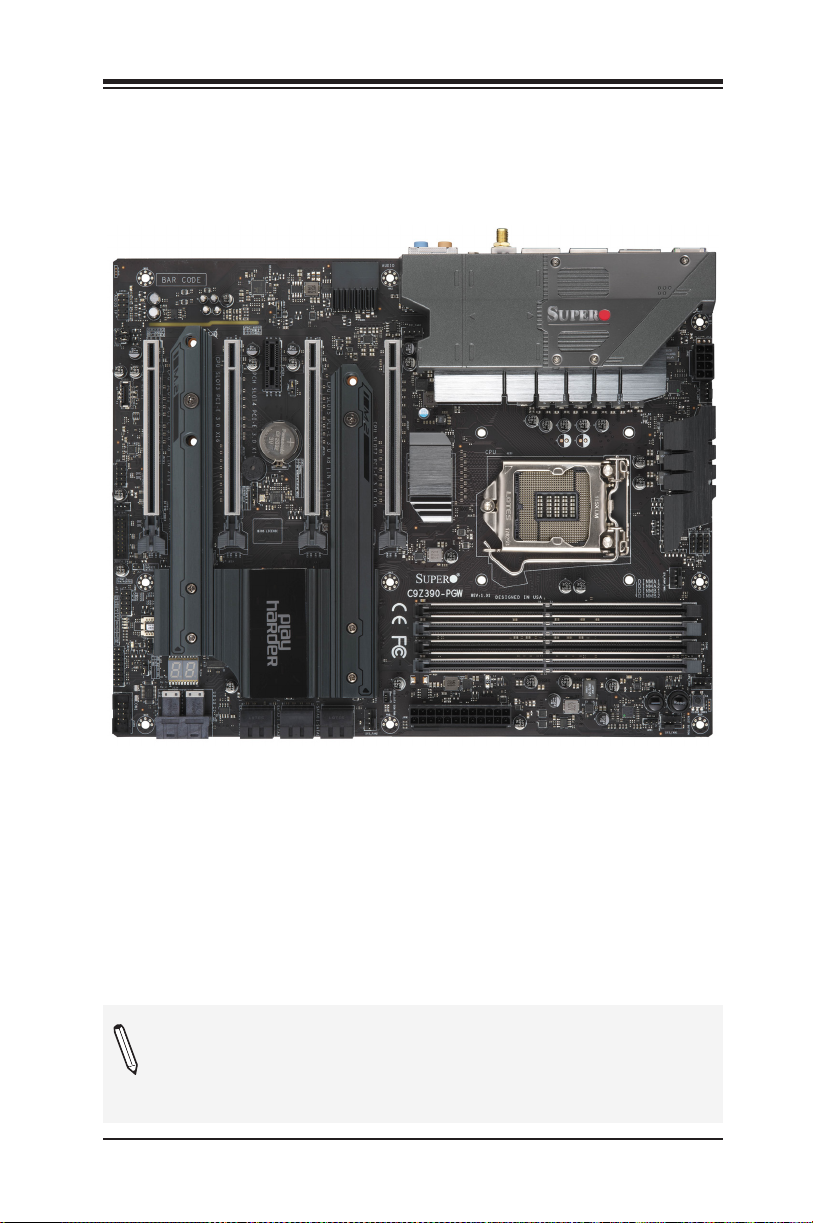
C9Z390-PGW Motherboard Image
Chapter 1: Introduction
Note: All graphics shown in this manual were based upon the latest
PCB Revision available at the time of publishing of the manual. The
motherboard you've received may or may not look exactly the same
as the graphics shown in this manual.
1-7
Page 20
Supermicro C9Z390-PGW Motherboard User’s Manual
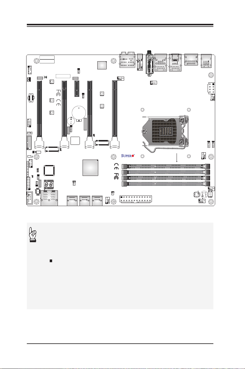
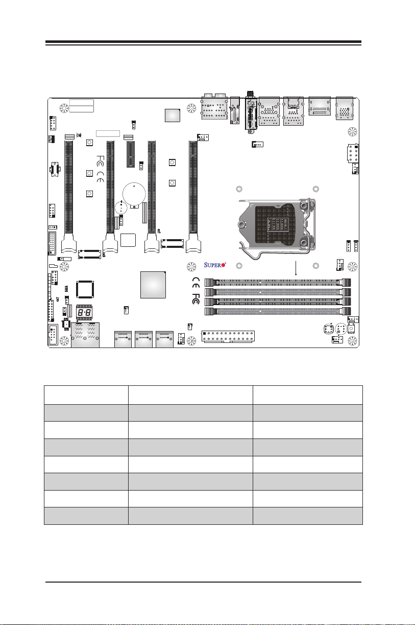
C9Z390-PGW Motherboard Layout
JI2C2
JI2C1
JSTBY1
JTPM1:
TPM/PORT80
PWR
LED
HDD
LED
NIC
1
NIC
2
3 PIN POWER LED
JLED1:
RSTOH/FF X
PWR
ON
JF1
AUDIO FP
USB 8 (3.1)
USB0/1
JL1
JTPM1
CPU LED
DIMM LED
VGA LED
BOOT LED
JLED1
LED1
JWD1
C
COM1
A
JCOM1
JI2C1/JI2C2
ON :ENABLE
OFF:DISABLE
JL1:
CHASSIS
INTRUSION
2-3:NMI
1-2:RST
A
U47
C
MAC CODE
MAC CODE
JWD1:
WATCH DOG
JPAC1
BAR CODE
JPAC1:AUDIO
MH10
CPU SLOT1 PCI-E 3.0 X8 (IN X16)
22110
MH11
2280
MH12
2260
JSTBY1:
USB 9/10(3.0)
5V STBY POWER
PCIE M.2-M1
LED4
LED4
PRESS FIT
U.2-1
U.2-2
1-2:ENABLE
2-3:DISABLE
CPU SLOT3 PCI-E 3.0 X16
PCH SLOT4 PCI-E 3.0 X1
SP1
SP1
JD1:
SPEAKER:1-4
BUZZER:3-4
JD1
BIOS LICENSE
A
C
LED3
I-SATA4
I-SATA5
+
B1
JRLED2
JPME2
I-SATA2
I-SATA3
JPME2:
2-3:ME MANUFACTURING MODE
1-2:NORMAL
C
HD AUDIO
SYS_FAN3
CPU SLOT5 PCI-E 3.0 X8 (IN X 16)
MH15
2280
DESIGNED IN USA
MH13
CPU SLOT7 PCI-E 3.0 X16
2260
LED2
A
PCIE M.2-M2
C9Z390-PGW
SATA DOM PWRJSD1:
JSD1
JPW1
MH8
I-SATA0
I-SATA1
SYS_FAN2
HDMI
REV:1.01A
PCIE M.2-E1
WIFI+BT
DESIGNED IN USA
LAN2
USB 6/7 (3.1)
JRLED1
LAN1
USB 4/5 (3.1)
DIMMA1
DIMMA2
DIMMB1
DIMMB2
Important Notes to the User
• See Chapter 2 for detailed information on jumpers, I/O ports and
JF1 front panel connections.
DP1/2
POWER
BUTTON
KB/MOUSE
USB 2/3(3.0)
JPW2
CPU_FAN2
JRLED3
12V_PUMP_PWR1
RESET
BUTTON
CLEAR CMOS
SYS_FAN1
DIMMA1
DIMMA2
DIMMB1
DIMMB2
CPU_FAN1
JRLED4
• " " indicates the location of "Pin 1".
• Jumpers not indicated are for testing only.
• When LED1 (Onboard Power LED Indicator) is on, system power
is on. Unplug the power cable before installing or removing any
components.
1-8
Page 21
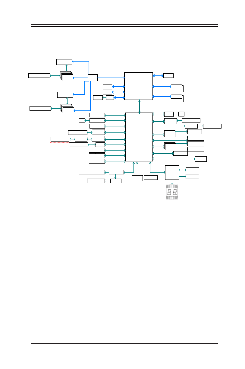
C9Z390-PGW Block Diagram
2 X USB 3.0 Rear
480Mbps
USB2.0
1 X USB 2.0 Header
480Mbps
USB2.0
2666/2400MHz
INTEL LGA1151
PCIe3.0_x16
8.0GT/s
SVID
IMVP8
DDR4 (CHA)
DIMMA0
DDR4 (CHB)
DIMMB0
2666/2400MHz
8GT/s
x4 DMI
RJ45
8GT/s
I219
PCH
Intel
CNL PCH-H
Z390
(Socket-H4)
AZALIA
Realtek ALC1220
FLASH
SPI 128Mb
SPI LPC
DIMMA1
DIMMB1
COM1 Header
NCT6792D-B
LPC I/O
TUSB1002
repeater x2
10Gbps
USB3.1_x2
USB 3.1 Rear Type-A
PCIe x1 SLOT #4
8GT/s
PCIe3.0_x1
8GT/s
PCIe3.0_x2
USB3.0
5Gbps
2 X USB 3.1 Rear Type-A
PS2 KB/MS
4 X SATA-III
SATA-III 6Gb/s
Audio Jack / Audio Pin Header
ASM1543
USB3
.1 Rear Type-C
8GT/s
PCIe3.0_x2
2 X USB 3.0 Header
USB3.1_x2
10Gbps
TUSB1002
repeater x2
8GT/s
ASM1480
U.2 SOCKET SSD
M.2 SOCKET SSD
ASMedia Switch
ASM1480
8GT/s
PCIe3.0_x2
2 X SATA-III
SATA-III
6Gb/s
M.2 SOCKET SSD
PCIe3.0_x2
8GT/s
(SATA-III)
U.2 SOCKET SSD
8GT/s
PCIe3.0_x4
AMP
Head Phone Header
PLX8747
ASMedia Switch
ASM1480
8.0GT/s
PCIe3.0_x8
PCIe x16 SLOT #7
8.0GT/s
PCIe3.0_x8
8.0GT/s
PCIe3.0_x8
PCIe3.0_x8
8.0GT/s
PCIe x 8 (in x16) SLOT #5
ASMedia Switch
ASM1480
8.0GT/s
PCIe x16 SLOT #3
PCIe3.0_x8
8.0GT/s
8.0GT/s
PCIe3.0_x8
PCIe3.0_
x8
8.0GT/s
PCIe3.0_x8
PCIe x 8 (in x16) SLOT #1
10G LAN2
AQC107
RJ45
USB3.1_x2
10Gbps
TUSB1002
repeater
M.2 key E
for WLAN + BT
CNVi interface
TPM1.2 Header
Display Port
Display Port
DDI1
DDI2
PS175
HDMI 2.0
DDI3
SMBUS
RENESAS
R5F104AC
On board LED and Header
USB 3.1 Type-C Header
ASM1543
PCIe3.0_x1
1G LAN1
PCIe3.0_x4
ASMedia Switch
Chapter 1: Introduction
1-9
Page 22
Supermicro C9Z390-PGW Motherboard User’s Manual
C9Z390-PGW Quick Reference
JI2C2
JI2C1
JSTBY1
JTPM1:
TPM/PORT80
PWR
LED
HDD
LED
NIC
1
NIC
2
3 PIN POWER LED
JLED1:
RSTOH/FF X
PWR
ON
JF1
AUDIO FP
USB 8 (3.1)
USB0/1
JL1
JTPM1
CPU LED
DIMM LED
VGA LED
BOOT LED
JLED1
LED1
JWD1
C
COM1
A
JCOM1
JI2C1/JI2C2
ON :ENABLE
OFF:DISABLE
JL1:
CHASSIS
INTRUSION
U47
MAC CODE
MAC CODE
2-3:NMI
1-2:RST
JWD1:
WATCH DOG
A
C
BAR CODE
JPAC1:AUDIO
MH10
CPU SLOT1 PCI-E 3.0 X8 (IN X16)
22110
1-2:ENABLE
2-3:DISABLE
CPU SLOT3 PCI-E 3.0 X16
PCH SLOT4 PCI-E 3.0 X1
MH11
2280
MH12
SP1
2260
JSTBY1:
USB 9/10(3.0)
5V STBY POWER
PCIE M.2-M1
LED4
PRESS FIT
U.2-1
U.2-2
LED4
SP1
JD1:
SPEAKER:1-4
BUZZER:3-4
JD1
BIOS LICENSE
A
C
LED3
I-SATA4
I-SATA5
JPAC1
JRLED2
+
B1
JPME2
I-SATA2
I-SATA3
JPME2:
2-3:ME MANUFACTURING MODE
1-2:NORMAL
HD AUDIO
SYS_FAN3
CPU SLOT5 PCI-E 3.0 X8 (IN X 16)
MH15
DESIGNED IN USA
MH13
CPU SLOT7 PCI-E 3.0 X16
2280
2260
LED2
A
C
PCIE M.2-M2
C9Z390-PGW
SATA DOM PWRJSD1:
JSD1
JPW1
MH8
I-SATA0
I-SATA1
SYS_FAN2
HDMI
REV:1.01A
PCIE M.2-E1
WIFI+BT
DESIGNED IN USA
LAN2
USB 6/7 (3.1)
JRLED1
LAN1
USB 4/5 (3.1)
DIMMA1
DIMMA2
DIMMB1
DIMMB2
DP1/2
POWER
BUTTON
Jumper Description Default
CLEAR CMOS Clear CMOS Switch Push Button Switch
JI2C1/JI2C2 SMB to PCI Slots Open (Disable)
JPAC1 Audio Enable Pins 1-2 (Enabled)
JPME2 Intel® Manufacturing Mode Pins 1-2 (Normal)
JWD1 Watch Dog Function Enable Pins 1-2 (RST)
POWER BUTTON Internal Power Button Push Button Switch
RESET BUTTON Onboard System Reset Button Push Button Switch
KB/MOUSE
USB 2/3(3.0)
JPW2
CPU_FAN2
JRLED3
12V_PUMP_PWR1
RESET
BUTTON
CLEAR CMOS
SYS_FAN1
DIMMA1
DIMMA2
DIMMB1
DIMMB2
JRLED4
CPU_FAN1
1-10
Page 23
Chapter 1: Introduction
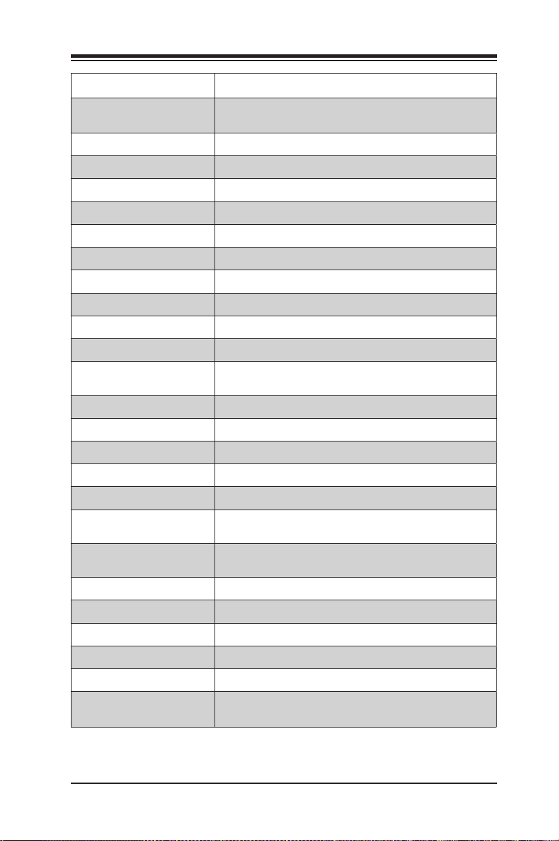
Connector Description
12V PUMP PWR1 12V 4-pin power connector for CPU pump of liquid
AUDIO FP Front Panel Audio Header
B1 Onboard Battery
COM1 COM1 Header
CPU SLOT1, 5 PCI Express x16 Slots (PCI-E 3.0 x8 link )
CPU SLOT3, 7 PCI Express x16 Slots (PCI-E 3.0 x16 link)
PCH SLOT4 PCI-E 3.0 x1 Slot
HD Audio High Denition Audio Ports
HDMI High Denition Multimedia Interface
DP1/2 DisplayPort Ports
I-SATA0-5 Intel® Z390 SATA 3.0 Ports (6Gb/sec)
JD1 External Speaker Header (Pins 1-4: External Speaker,
JF1 Front Control Panel Header
JL1 Chassis Intrusion Header
JLED1 Power LED Indicator Header
JPW1 24-pin ATX Main Power Connector (Required)
JPW2 +12V 8-pin CPU power Connector (Required)
JRLED1/2 JRLED1 connects to I/O cover's RGB board; JRLED2
JRLED3/4 External 12V RGB strip (see Ch. 2 for installation
JSD1 SATA DOM (Disk-On-Module) Power Connector
JSTBY1 Standby Power Header
JTPM1 Trusted Platform Module (TPM) Header
KB/MOUSE PS2 Keyboard/Mouse Connectors
LAN1/LAN2 RJ45 Gigabit LAN Ports
PCI-E M.2-E1 PCI-E M.2 E1 key connector for WiFi module (pre-
cooling
Pins 3-4:Buzzer)
connects to PCH RGB board
instructions)
installed)
1-11
Page 24
Supermicro C9Z390-PGW Motherboard User’s Manual
PCI-E M.2-M1,M2 PCI-E M.2 Connectors 1 and 2, small form factor devices
System FAN 1,2,3/CPU
FAN 1,2
U.2-1, U.2-2 U.2 Connector 1 and 2, for 2.5” SSD Drives
USB0/1 Front access USB 2.0 header
USB2/3 Back panel USB 3.1 Gen 1 ports
USB4/5, USB6/7 Back panel USB 3.1 Gen 2 por ts
USB8 Front access USB 3.1 Gen 2 header
USB9/10 Front access USB 3.1 Gen 1 header
and other portable devices for high speed NVMe SSDs
(M1 shares link with U.2-1 port; M2 shares link with
I-SATA4/5 port)
System/CPU Headers
LED Description Color/State
BOOT LED Bootable Device POST Status Red ON: BOOT POST Activity
CPU LED CPU POST Status Yellow ON: CPU POST Activity
DIMM LED DIMM POST Status Blue ON: DIMM POST Activity
VGA LED Onboard VGA POST Status Green ON: VGA POST Activity
LED1 Onboard Standby PWR LED Green ON: On
LED2 M.2 connector 2 SSD ACT LED Green Blinking: Activity
LED3 M.2 connector 1 SSD ACT LED Green Blinking: Activity
LED4 Status Code LED* Digital Readout
*Download the AMI status codes at https://ami.com/ami_downloads/
Aptio_V_Status_Codes.pdf
1-12
Page 25
Chapter 2: Installation
Chapter 2
Installation
2-1 Installation Components and Tools Needed
Screws
Intel LGA 1151 Processor
PC Chassis
Power Supply
Phillips-Head Screwdriver
DDR4 DIMMs
Heatsink with Fan
Video Card (Optional)
SATA/USB Optical Drive (Optional)
SATA Hard Disk Drive
2-1
Page 26

Supermicro C9Z390-PGW Motherboard User’s Manual
2-2 Static-Sensitive Devices
Electrostatic Discharge (ESD) can damage electronic com ponents. To
avoid damaging your system board, it is important to handle it very
carefully. The following measures are generally sufcient to protect your
equipment from ESD.
Precautions
• Use a grounded wrist strap designed to prevent static discharge.
• Touch a grounded metal object before removing the board from the
antistatic bag.
• Handle the board by its edges only; do not touch its components,
peripheral chips, memory modules or gold contacts.
• When handling chips or modules, avoid touching their pins.
• Put the motherboard and peripherals back into their antistatic bags
when not in use.
• For grounding purposes, make sure your computer chassis provides
excellent conductivity between the power supply, the case, the mounting fasteners and the motherboard.
• Use only the correct type of onboard CMOS battery. Do not install the
onboard battery upside down to avoid possible explosion.
Unpacking
The motherboard is shipped in antistatic packaging to avoid static damage. When unpacking the board, make sure that the person handling it
is static protected.
2-2
Page 27
Chapter 2: Installation
2-3 Processor and Heatsink Installation
Attention! When handling the processor package, avoid placing
direct pressure on the label area of the fan.
Important:
Always connect the power cord last, and always remove it before
adding, removing or changing any hardware components. Make
sure that you install the processor into the CPU socket before
you install the CPU heatsink.
If you buy a CPU separately, make sure that you use an Intel-
certied multi-directional heatsink only.
Make sure to install the system board into the chassis before
you install the CPU heatsink.
When receiving a server board without a processor pre-installed,
make sure that the plastic CPU socket cap is in place and none
of the socket pins are bent; otherwise, contact your retailer
immediately.
Refer to the Supermicro website for updates on CPU support.
Installing the LGA1151 Processor
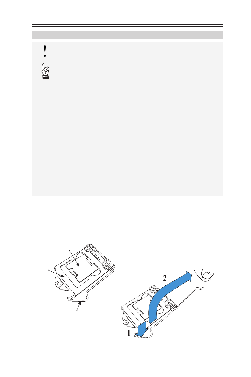
1. Press the load lever to release the load plate, which covers the CPU
socket, from its locking position.
Plastic Cap
Load Plate
Load Lever
2-3
Page 28
Supermicro C9Z390-PGW Motherboard User’s Manual
2. Gently lift the load lever to open the load plate. Remove the plastic cap.
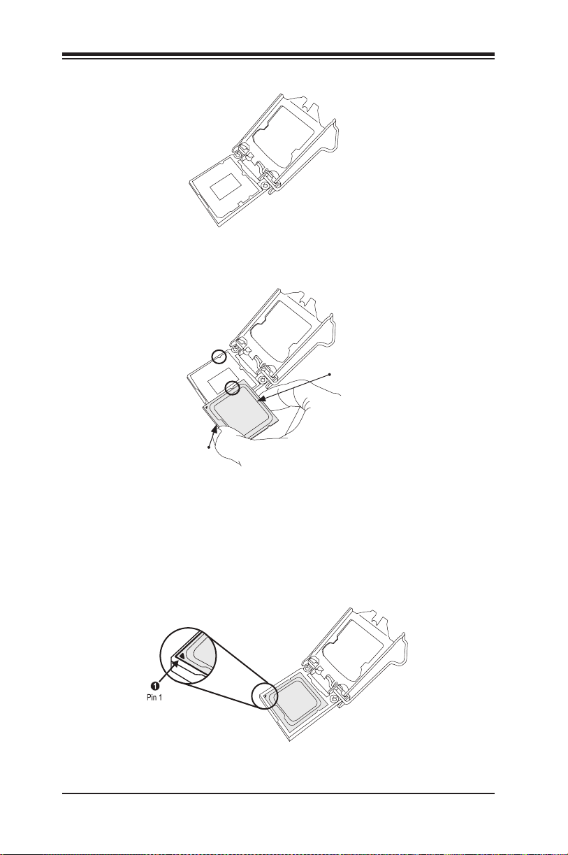
3. Use your thumb and your index nger to hold the CPU at the North
center edge and the South center edge of the CPU.
North Center Edge
South Center Edge
4. Align the small triangle marker on the CPU to its corresponding triangle marker on the load bracket. Once it is aligned, carefully lower
the CPU straight down into the socket. (Do not drop the CPU on the
socket, or move it horizontally or vertically.)
2-4
Page 29

Chapter 2: Installation
5. Do not rub the CPU against the surface or against any pins of the
socket to avoid damaging the CPU or the socket.)
6. With the CPU inside the socket, inspect the four corners of the CPU
to make sure that the CPU is properly installed.
7. Use your thumb to gently push the load lever down to the lever
lock.
8. Close the load plate with the CPU inside the socket. Lock the "Close
1st" lever rst, then lock the "Open 1st" lever second. Gently push
the load levers down to the lever locks.
CPU properly
installed
Load lever locked
into place
Attention! You can only install the CPU inside the socket in one direction. Make sure that it is properly inserted into the CPU socket before
closing the load plate. If it doesn't close properly, do not force it as it
may damage your CPU. Instead, open the load plate again and doublecheck that the CPU is aligned properly.
2-5
Page 30
Supermicro C9Z390-PGW Motherboard User’s Manual
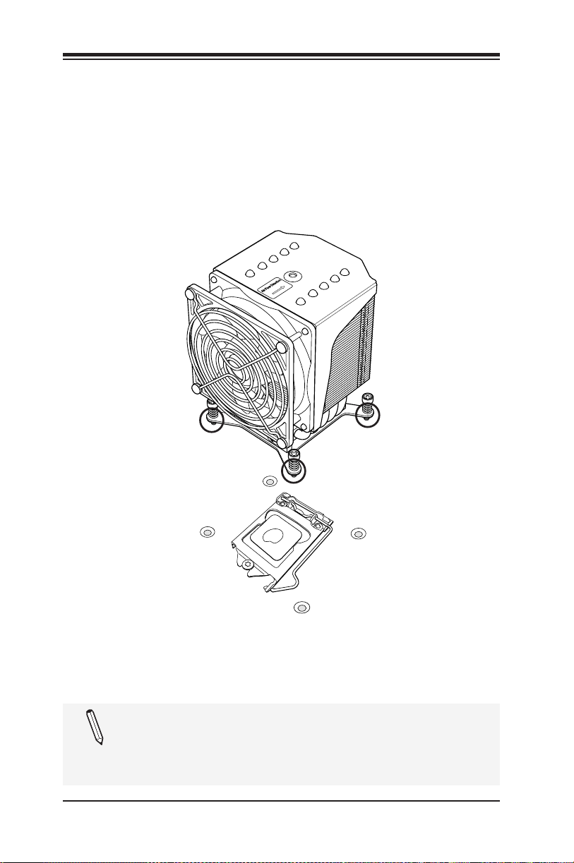
Installing an Active CPU Heatsink with Fan
1. Apply the proper amount of thermal grease to the heatsink.
2. Place the heatsink on top of the CPU so that the four mount-
ing holes on the heatsink are aligned with those on the retention
mechanism.
3. Tighten the screws in the following order:
Screw #4
Screw #3
Screw #2
4. Once the screws are tightened, plug the power cord into the FAN1
connector.
Note: Screw #1 is not shown in the illustration.
Note: Graphic drawings included in this manual are for reference
only. They might look different from the components installed in
your system.
2-6
Page 31

Chapter 2: Installation
Removing an Active CPU Heatsink with Fan
Warning: We do not recommend that the CPU or heatsink be removed.
However, if you do need to remove the heatsink, please follow the instruction below to uninstall the heatsink to avoid damaging the CPU or other
components.
1. Unplug the power cord from the power supply.
2. Loosen the screws in the order below.
3. Gently wiggle the heatsink to loosen it. Do not use excessive force
when wiggling the heatsink.
Screw #4
Screw #3
Screw #2
4. Once the heatsink is loosened, remove it from the motherboard.
Note: Screw #1 is not shown in the illustration.
2-7
Page 32

Supermicro C9Z390-PGW Motherboard User’s Manual
2-4 Installing DDR4 Memory
Note: Check the Supermicro website for recommended memory
modules.
Attention! Exercise extreme care when installing or removing
DIMM modules to prevent any possible damage.
DIMM Installation
1. Insert the desired number of
DIMMs into the memory slots,
starting with DIMMA2 and
DIMMB2, then DIMMA1 and
DIMMB1. For the system to
work properly, please use the
memory modules of the same
type and speed in the same
motherboard.
2. Push the release tabs outwards
on both ends of the DIMM slot
to unlock it.
3. Align the key of the DIMM module with the receptive point on the
memory slot.
JI2C2
JI2C1
JSTBY1
JTPM1:
TPM/PORT80
PWR
LED
LED
NIC
1
NIC
2
RSTOH/FF X
PWR
ON
AUDIO FP
JI2C1/JI2C2
ON :ENABLE
OFF:DISABLE
USB 8 (3.1)
USB0/1
JL1
JL1:
CHASSIS
INTRUSION
JTPM1
HDD
3 PIN POWER LED
JLED1:
CPU LED
DIMM LED
VGA LED
BOOT LED
JLED1
LED1
JWD1
C
JF1
COM1
U47
A
JCOM1
MAC CODE
MAC CODE
BAR CODE
MH10
CPU SLOT1 PCI-E 3.0 X8 (IN X16)
22110
MH11
2280
MH12
2260
JSTBY1:
USB 9/10(3.0)
5V STBY POWER
PCIE M.2-M1
2-3:NMI
1-2:RST
JWD1:
LED4
WATCH DOG
LED4
A
PRESS FIT
C
U.2-1
U.2-2
CPU SLOT3 PCI-E 3.0 X16
PCH SLOT4 PCI-E 3.0 X1
SP1
SP1
JD1:
SPEAKER:1-4
BUZZER:3-4
JD1
BIOS LICENSE
A
C
LED3
I-SATA4
I-SATA5
JPAC1
JPAC1:AUDIO
1-2:ENABLE
2-3:DISABLE
JRLED2
JPME2
JPME2:
2-3:ME MANUFACTURING MODE
1-2:NORMAL
+
B1
I-SATA2
I-SATA3
SYS_FAN3
CPU SLOT5 PCI-E 3.0 X8 (IN X 16)
MH15
2280
DESIGNED IN USA
MH13
2260
LED2
A
C
PCIE M.2-M2
SATA DOM PWRJSD1:
JSD1
SYS_FAN2
MH8
I-SATA0
I-SATA1
HD AUDIO
CPU SLOT7 PCI-E 3.0 X16
C9Z390-PGW
JPW1
PCIE M.2-E1
HDMI
REV:1.01A
WIFI+BT
DESIGNED IN USA
USB 6/7 (3.1)
JRLED1
DP1/2
KB/MOUSE
USB 2/3(3.0)
LAN2
LAN1
USB 4/5 (3.1)
JPW2
CPU_FAN2
JRLED4
JRLED3
12V_PUMP_PWR1
DIMMA1
DIMMA2
DIMMB1
DIMMA1
DIMMB2
DIMMA2
DIMMB1
DIMMB2
POWER
RESET
CPU_FAN1
BUTTON
BUTTON
CLEAR CMOS
SYS_FAN1
4. Align the notches on both ends of
the module against the receptive
points on the ends of the slot.
5. Use two thumbs together to press
the notches on both ends of the
module straight down into the slot
until the module snaps into place.
6. Press the release tabs to the lock
positions to secure the DIMM module into the slot.
Removing Memory Modules
Reverse the steps above to remove the
DIMM modules from the motherboard.
2-8
Notches
Release Tabs
Press both notches
straight down into
the memory slot.
Page 33

JPW2
DIMMB2
DIMMA2
DIMMA1
DIMMB1
HD AUDIO
USB 6/7 (3.1)
LAN1
USB 4/5 (3.1)
LAN2
DIMMB2
DIMMB1
DIMMA2
DIMMA1
CPU_FAN2
KB/MOUSE
USB 2/3(3.0)
DP1/2
HDMI
PCIE M.2-E1
JRLED1
12V_PUMP_PWR1
JRLED3
JRLED4
DESIGNED IN USA
WIFI+BT
REV:1.01A
Chapter 2: Installation
Memory Support
Towards the CPU
DIMMA1
DIMMA2
DIMMB1
DIMMB2
Th e C9Z39 0 -PGW supp orts up to 64GB of Unbu f fered (UDIMM) non- ECC
DDR4 memory, up to 2666/2400MHz or 4000+MHz (OC) in four 288-pin
memory slots. Populating these DIMM modules with a pair of memory
modules of the same type and size will result in interleaved memory,
which will improve memory performance.
Note: Be sure to use memory modules of the same type, speed,
and frequency on the motherboard. Mixing of memory modules of
different types and speeds is not allowed.
2-9
Page 34

Supermicro C9Z390-PGW Motherboard User’s Manual
Memory Population Guidelines
When installing memory modules, the DIMM slots should be populated in
the following order: DIMMA2, DIMMB2, then DIMMA1, DIMMB1.
• Always use DDR4 DIMM modules of the same size and speed.
• Mixed DIMM speeds can be installed. However, all DIMMs will run at the
speed of the slowest DIMM.
DIMMA2
DIMMA1
Towards the CPU
DIMMB2
DIMMB1
Recommended
Population
One DIMM
Two DIMM
Four DIMM
2-10
Page 35

Chapter 2: Installation
2-4 M.2 Installation (optional)
Two M.2 (M-key) connectors are supported by the C9Z390-PGW. M.2
devices are used for solid state storage and internal expansion. Follow
the steps below in order to install an M.2 device.
1. Locate and remove the retaining
screws on the M.2 heatsink.
2. With the heatsink removed, locate
the standoff.
3. If required, remove the standoff
and move to appropriate location
for M.2 card's length.
4. Carefully plug the M.2 device into
the M.2 connector and lower the
semi-circle notched end onto the
standoff.
5. Remove the M.2 heatsink thermal
tape cover.
6. Replace the M.2 heatsink and
the retaining screws. Tighten the
screws to secure the heatsink into
place.
2-11
Page 36

Supermicro C9Z390-PGW Motherboard User’s Manual
2-5 Motherboard Installation
All motherboards have standard mounting holes to t different types of
chassis. Make sure that the locations of all the mounting holes for both
motherboard and chassis match. Although a chassis may have both plastic and metal mounting fasteners, metal ones are highly recommended
because they ground the motherboard to the chassis. Make sure that the
metal standoffs click in or are screwed in tightly. Then use a screwdriver
to secure the motherboard onto the motherboard tray.
Philips Screwdriver (1)
Tools Needed
MAC CODE
MAC CODE
AUDIO FP
JI2C2
JI2C1
JSTBY1
JTPM1:
TPM/PORT80
PWR
LED
HDD
LED
NIC
1
NIC
2
3 PIN POWER LED
RSTOH/FF X
PWR
ON
JLED1:
DIMM LED
BOOT LED
JF1
USB0/1
CPU LED
VGA LED
LED1
COM1
JCOM1
JI2C1/JI2C2
ON :ENABLE
OFF:DISABLE
USB 8 (3.1)
JL1
JL1:
CHASSIS
INTRUSION
JTPM1
JLED1
JWD1
C
U47
A
BAR CODE
MH10
CPU SLOT1 PCI-E 3.0 X8 (IN X16)
22110
MH11
2280
MH12
2260
JSTBY1:
USB 9/10(3.0)
5V STBY POWER
A
C
LED3
PCIE M.2-M1
2-3:NMI
1-2:RST
JWD1:
LED4
WATCH DOG
LED4
A
PRESS FIT
C
U.2-1
U.2-2
JPAC1:AUDIO
1-2:ENABLE
2-3:DISABLE
CPU SLOT3 PCI-E 3.0 X16
PCH SLOT4 PCI-E 3.0 X1
SP1
SP1
JD1:
SPEAKER:1-4
BUZZER:3-4
JD1
BIOS LICENSE
I-SATA4
I-SATA5
JPAC1
JRLED2
+
B1
JPME2
I-SATA2
I-SATA3
JPME2:
2-3:ME MANUFACTURING MODE
1-2:NORMAL
Philips Screws (9)
HD AUDIO
MH15
2280
DESIGNED IN USA
MH13
2260
A
PCIE M.2-M2
SYS_FAN2
SYS_FAN3
CPU SLOT7 PCI-E 3.0 X16
C9Z390-PGW
SATA DOM PWRJSD1:
JSD1
JPW1
MH8
CPU SLOT5 PCI-E 3.0 X8 (IN X 16)
LED2
C
I-SATA0
I-SATA1
HDMI
REV:1.01A
PCIE M.2-E1
WIFI+BT
DESIGNED IN USA
LAN2
USB 6/7 (3.1)
JRLED1
Standoffs (9)
Only if Needed
DP1/2
KB/MOUSE
DIMMA1
DIMMA2
DIMMB1
DIMMB2
POWER
BUTTON
USB 2/3(3.0)
SYS_FAN1
LAN1
USB 4/5 (3.1)
JPW2
CPU_FAN2
JRLED3
12V_PUMP_PWR1
DIMMA1
DIMMA2
DIMMB1
DIMMB2
RESET
CPU_FAN1
BUTTON
CLEAR CMOS
JRLED4
Location of Mounting Holes
Attention! 1) To avoid damaging the motherboard and its com-
ponents, please do not use a force greater than 8 lb/inch on each
mounting screw during motherboard installation. 2) Some components are very close to the mounting holes. Please take precautionary
measures to avoid damaging these components when installing the
motherboard to the chassis.
2-12
Page 37

Chapter 2: Installation
Installing the Motherboard
1. Install the I/O shield into the back of the chassis.
2. Locate the mounting holes on the motherboard. (See the previous
page.)
3. Locate the matching mounting holes on the chassis. Align the
mounting holes on the motherboard against the mounting holes on
the chassis.
4. Install standoffs in the chassis as needed.
5. Install the motherboard into the chassis carefully to avoid damaging
other motherboard components.
6. Using the Phillips screwdriver, insert a Phillips head #6 screw into a
mounting hole on the motherboard and its matching mounting hole
on the chassis.
7. Repeat Step 6 to insert remaining screws into all mounting holes.
8. Make sure that the motherboard is securely placed in the chassis.
Note: Images displayed are for illustration only. Your chassis
or components might look different from those shown in this
manual.
2-13
Page 38

Supermicro C9Z390-PGW Motherboard User’s Manual
2-6 Connectors/IO Ports
The I/O ports are color coded in conformance with the industry standards.
See the gure below for the colors and locations of the various I/O ports.
Back I/O Panel
JI2C2
JI2C1
JSTBY1
JTPM1:
TPM/PORT80
PWR
LED
HDD
LED
NIC
1
NIC
2
3 PIN POWER LED
JLED1:
RSTOH/FF X
PWR
ON
AUDIO FP
USB0/1
JTPM1
CPU LED
DIMM LED
VGA LED
BOOT LED
LED1
JWD1
JF1
COM1
JCOM1
MAC CODE
MAC CODE
JI2C1/JI2C2
ON :ENABLE
OFF:DISABLE
USB 8 (3.1)
JL1
JL1:
CHASSIS
INTRUSION
JLED1
2-3:NMI
1-2:RST
JWD1:
WATCH DOG
A
C
U47
A
C
BAR CODE
JPAC1:AUDIO
MH10
CPU SLOT1 PCI-E 3.0 X8 (IN X16)
22110
MH11
2280
MH12
2260
JSTBY1:
USB 9/10(3.0)
5V STBY POWER
PCIE M.2-M1
LED4
LED4
PRESS FIT
U.2-1
U.2-2
1-2:ENABLE
2-3:DISABLE
CPU SLOT3 PCI-E 3.0 X16
PCH SLOT4 PCI-E 3.0 X1
SP1
SP1
JD1:
SPEAKER:1-4
BUZZER:3-4
JD1
BIOS LICENSE
A
C
LED3
I-SATA4
I-SATA5
JPAC1
JRLED2
+
B1
JPME2
I-SATA2
I-SATA3
JPME2:
2-3:ME MANUFACTURING MODE
1-2:NORMAL
HD AUDIO
MH15
2280
DESIGNED IN USA
MH13
2260
SYS_FAN3
CPU SLOT7 PCI-E 3.0 X16
CPU SLOT5 PCI-E 3.0 X8 (IN X 16)
LED2
A
C
PCIE M.2-M2
C9Z390-PGW
SATA DOM PWRJSD1:
JSD1
JPW1
MH8
I-SATA0
I-SATA1
SYS_FAN2
HDMI
REV:1.01A
PCIE M.2-E1
WIFI+BT
DESIGNED IN USA
LAN2
USB 6/7 (3.1)
JRLED1
LAN1
USB 4/5 (3.1)
DIMMA1
DIMMA2
DIMMB1
DIMMB2
DP1/2
POWER
BUTTON
KB/MOUSE
USB 2/3(3.0)
JPW2
CPU_FAN2
JRLED3
12V_PUMP_PWR1
RESET
BUTTON
CLEAR CMOS
SYS_FAN1
DIMMA1
DIMMA2
DIMMB1
DIMMB2
CPU_FAN1
JRLED4
A. PS/2 Keyboard/Mouse Port G. USB 3.1 Gen 2 Port 4 M. Center/LFE Out
B. USB 3.1 Gen 1 Port 2 H. USB 3.1 Gen 2 Port 5 N. Surround Out
C. USB 3.1 Gen 1 Port 3 I. LAN2 O. S/PDIF Out
D. DisplayPort 1 J. USB 3.1 Gen 2 Port 6 P. Line In
E. DisplayPort 2 K. USB 3.1 Gen 2 Port 7 Q. Line Out
F. LAN1 L. HDMI Port R. Mic In
M
A
F
I
P
D
Q
B
E
C
G
H
J
K
2-14
N
L
O
R
Page 39

Chapter 2: Installation
Universal Serial Bus (USB)
Four USB 3.1 Gen 2 ports (#4/5/6/7) and two USB 3.1 Gen 1 ports (#2/3)
are located on the I/O back panel. In addition, one front panel USB 3.1
Gen 2 header (#8), one USB 3.1 Gen 1 header (two ports: #9/10), one
USB 2.0 header (two ports: #0/1) are also located on the motherboard
to provide front chassis access using USB cables (not included). See the
tables below for pin denitions.
Front Panel USB (2.0) Header #0/1
Pin Definitions
Pin# Denition Pin# Denition
1 +5V 2 +5V
3 USB_PN2 4 USB_PN3
5 USB_PP2 6 USB_PP3
7 Ground 8 Ground
9 Key 10 Ground
Back Panel USB (3.1 Gen 1) #2/3, USB (3.1
Gen 2) #4/5/6/7 Pin Definitions
Pin# Denition Pin# Denition
1 +5V 5 +5V
2 USB_PN1 6 USB_PN0
3 USB_PP1 7 USB_PP0
4 Ground 8 Ground
Front Panel USB (3.1 Gen 1) Header #9/10
Pin Definitions
Pin# Pin# Signal Name Description
1 10 VBUS Power
2 11 D- USB 2.0 Differential Pair
3 12 D+
4 13 Ground Ground of PWR Return
5 14 StdA_SSRX- SuperSpeed Receiver
6 15 StdA_SSRX+ Differential Pair
7 16 GND_DRAIN Ground for Signal Return
8 17 StdA_SSTX- SuperSpeed Transmitter
9 18 StdA_SSTX+ Differential Pair
A
B
CDE
F
G
H
AUDIO FP
JI2C2
JI2C1
USB0/1
JSTBY1
JTPM1:
TPM/PORT80
JTPM1
PWR
LED
HDD
LED
NIC
1
NIC
2
3 PIN POWER LED
JLED1:
CPU LED
DIMM LED
VGA LED
BOOT LED
RSTOH/FF X
PWR
ON
LED1
JWD1
JF1
COM1
JCOM1
A. Back panel USB 3.1 Gen1 #2
B. Back panel USB 3.1 Gen1 #3
C. Back panel USB 3.1 Gen2 #4
D. Back panel USB 3.1 Gen2 #5
E. Back panel USB 3.1 Gen2 #6
F. Back panel USB 3.1 Gen2 #7
G. USB 2.0 Header #0/1
H. USB 3.1 Gen1 Header #9/10
SYS_FAN3
CPU SLOT7 PCI-E 3.0 X16
C9Z390-PGW
SATA DOM PWRJSD1:
JSD1
JPW1
MH8
HD AUDIO
PCIE M.2-E1
HDMI
WIFI+BT
JRLED1
REV:1.01A
DESIGNED IN USA
MAC CODE
MAC CODE
JI2C1/JI2C2
ON :ENABLE
MH10
OFF:DISABLE
CPU SLOT1 PCI-E 3.0 X8 (IN X16)
22110
USB 8 (3.1)
MH11
2280
MH12
2260
JSTBY1:
USB 9/10(3.0)
5V STBY POWER
JL1
JL1:
CHASSIS
INTRUSION
PCIE M.2-M1
JLED1
2-3:NMI
1-2:RST
JWD1:
LED4
WATCH DOG
LED4
A
C
PRESS FIT
U47
A
C
U.2-1
U.2-2
BAR CODE
A
C
LED3
JPAC1
JPAC1:AUDIO
1-2:ENABLE
2-3:DISABLE
CPU SLOT3 PCI-E 3.0 X16
PCH SLOT4 PCI-E 3.0 X1
JPME2
SP1
2-3:ME MANUFACTURING MODE
SP1
+
B1
JD1:
SPEAKER:1-4
BUZZER:3-4
JD1
BIOS LICENSE
JRLED2
I-SATA4
I-SATA2
I-SATA5
I-SATA3
CPU SLOT5 PCI-E 3.0 X8 (IN X 16)
MH15
2280
DESIGNED IN USA
MH13
2260
JPME2:
1-2:NORMAL
LED2
A
C
PCIE M.2-M2
SYS_FAN2
I-SATA0
I-SATA1
LAN2
USB 6/7 (3.1)
LAN1
USB 4/5 (3.1)
DP1/2
KB/MOUSE
USB 2/3(3.0)
JPW2
CPU_FAN2
JRLED4
JRLED3
12V_PUMP_PWR1
DIMMA1
DIMMA2
DIMMB1
DIMMA1
DIMMB2
DIMMA2
DIMMB1
DIMMB2
POWER
RESET
CPU_FAN1
BUTTON
BUTTON
CLEAR CMOS
SYS_FAN1
2-15
Page 40

Supermicro C9Z390-PGW Motherboard User’s Manual
Front Panel USB (3.1 Gen 2 Type-C) Header #8
Pin Definitions
Pin# Denition Pin# Denition Pin# Denition
1 VBUS 8 CC1 15 RX2+
2 TX1+ 9 SBU1 16 RX2-
3 TX1- 10 SBU2 17 GND
4 GND 11 VBUS 18 D-
5 RX1+ 12 TX2+ 19 D+
6 RX1- 13 TX2- 20 CC2
7 VBUS 14 GND
A. USB8
HD AUDIO
HDMI
CPU SLOT7 PCI-E 3.0 X16
REV:1.01A
C9Z390-PGW
JPW1
PCIE M.2-E1
WIFI+BT
DESIGNED IN USA
LAN2
USB 6/7 (3.1)
JRLED1
LAN1
USB 4/5 (3.1)
DIMMA1
DIMMA2
DIMMB1
DIMMB2
DP1/2
POWER
BUTTON
KB/MOUSE
USB 2/3(3.0)
JPW2
CPU_FAN2
12V_PUMP_PWR1
RESET
BUTTON
CLEAR CMOS
SYS_FAN1
JRLED3
DIMMA1
DIMMA2
JRLED4
DIMMB1
DIMMB2
CPU_FAN1
MAC CODE
MAC CODE
AUDIO FP
JI2C2
JI2C1/JI2C2
ON :ENABLE
MH10
OFF:DISABLE
CPU SLOT1 PCI-E 3.0 X8 (IN X16)
JI2C1
A
USB 8 (3.1)
MH12
USB0/1
JSTBY1
JSTBY1:
USB 9/10(3.0)
5V STBY POWER
JL1
JL1:
CHASSIS
INTRUSION
PCIE M.2-M1
JTPM1:
TPM/PORT80
JTPM1
PWR
LED
HDD
LED
NIC
1
NIC
2
3 PIN POWER LED
JLED1:
CPU LED
DIMM LED
VGA LED
BOOT LED
RSTOH/FF X
JLED1
PWR
ON
LED1
2-3:NMI
1-2:RST
JWD1:
JWD1
WATCH DOG
LED4
A
C
JF1
COM1
PRESS FIT
U47
A
C
JCOM1
U.2-1
U.2-2
22110
MH11
2280
2260
LED4
BAR CODE
A
C
JPAC1
JPAC1:AUDIO
1-2:ENABLE
2-3:DISABLE
CPU SLOT3 PCI-E 3.0 X16
PCH SLOT4 PCI-E 3.0 X1
SP1
SP1
+
B1
JD1:
SPEAKER:1-4
BUZZER:3-4
JD1
BIOS LICENSE
LED3
JRLED2
I-SATA4
I-SATA5
CPU SLOT5 PCI-E 3.0 X8 (IN X 16)
JPME2
DESIGNED IN USA
JPME2:
2-3:ME MANUFACTURING MODE
1-2:NORMAL
LED2
A
C
PCIE M.2-M2
I-SATA2
I-SATA0
I-SATA1
I-SATA3
MH15
2280
MH13
2260
SYS_FAN2
SATA DOM PWRJSD1:
JSD1
SYS_FAN3
MH8
2-16
Page 41

Chapter 2: Installation
Back Panel High Denition Audio (HD Audio)
This motherboard features a 7.1+2 Channel High Denition Audio (HDA)
codec that provides 10 DAC channels. The HD Audio connections simultaneously supports multiple-streaming 7.1 sound playback with 2 chan-
nels of independent stereo output through the front panel stereo out for
front, rear, center and subwoofer speakers. Use the Advanced software
included in the CD-ROM with your motherboard to enable this function.
Audio Configuration
2 Channel 4.1 Channel 5.1 Channel 7.1 Channel
Light Blue
(Line In/Side Speaker Out)
(Line Out/Front Speaker Out)
Lime
Orange
(Center/Subwoofer)
Black
(Surround)
Pink (Mic In) Mic In Mic In Mic In Mic In
Line In Line In Line In
Line Out
Front
Speaker Out
Rear Speaker
Out
Front
Speaker Out
Center/
Subwoofer
Rear Speaker
Out
Side Speaker
Out
Front
Speaker Out
Center/
Subwoofer
Rear Speaker
Out
2-17
A. Line In
B. Line Out
C. Center/LFE Out
D. Surround Out
E. Mic In
A
C
D
B
E
Page 42

Supermicro C9Z390-PGW Motherboard User’s Manual
ATX PS/2 Keyboard/Mouse Port
The ATX PS/2 keyboard and PS/2 mouse are located above Back Panel
USB Ports 2/3 on the motherboard.
VESA® DisplayPort™
DisplayPort, develped by the VESA consortium, delivers digital display at
a fast refresh rate. It can connect to virtually any display device using a
DisplayPort adapter for devices such as VGA, DVI, or HDMI.
HDMI Port
One HDMI (High-Denition Multimedia Interface) is located on the I/O
back panel. This connector is used to display both high denition video
and digital sound through an HDMI capable display, using a single HDMI
cable (not included).
Ethernet Port
Two Gigabit Ethernet ports (LAN1/2) are located on the I/O back panel
to provide network connections. These ports will accept RJ45 type cables.
Note: Please refer to the LED Indicator Section for LAN LED infor-
mation.
LAN Ports
Pin Definition
Pin# Denition Pin# Denition Pin Denition
1 P2V5SB 7 TD2- 13 Link 100
2 TD0+ 8 TD3+ 14 Link 1000
3 TD0- 9 TD3- 15 Ground
4 TD1+ 10 SGND 16 Ground
5 TD1- 11 Act LED 17 Ground
6 TD2+ 12 P3V3SB 18 Ground
(NC: No Connection)
A
B
C
LED (Green,
+3V3SB)
LED (Yellow,
+3V3SB)
2-18
A. PS/2 Keyboard/Mouse Port
B. Display Port #1
C. Display Port #2
D. LAN1
E. LAN2
F. HDMI Port
D
E
F
Page 43

Chapter 2: Installation
OH/Fan Fail L
OH/Fan Fail LED(+)
1516
Front Control Panel
JF1 contains header pins for various buttons and indicators that are
normally located on a control panel at the front of the chassis. These
connectors are designed specically for use with Supermicro chassis. See
the gure below for the descriptions of the front control panel buttons
and LED indicators. Refer to the following section for descriptions and
pin denitions.
JI2C2
JI2C1
JSTBY1
JTPM1:
TPM/PORT80
PWR
LED
HDD
LED
NIC
1
NIC
2
3 PIN POWER LED
RSTOH/FF X
PWR
ON
AUDIO FP
USB0/1
JTPM1
JLED1:
CPU LED
DIMM LED
VGA LED
BOOT LED
LED1
JWD1
JF1
COM1
JCOM1
USB 8 (3.1)
MAC CODE
MAC CODE
JI2C1/JI2C2
ON :ENABLE
OFF:DISABLE
JL1
JL1:
CHASSIS
INTRUSION
JLED1
2-3:NMI
1-2:RST
JWD1:
WATCH DOG
A
C
U47
A
C
Power LED (-)
HDD LED (-)
NIC2 LED (-)
NIC1 LED (-)
BAR CODE
JPAC1:AUDIO
LED4
A
C
LED3
1-2:ENABLE
2-3:DISABLE
CPU SLOT3 PCI-E 3.0 X16
PCH SLOT4 PCI-E 3.0 X1
SP1
SP1
JD1:
SPEAKER:1-4
BUZZER:3-4
JD1
BIOS LICENSE
I-SATA4
I-SATA5
MH10
CPU SLOT1 PCI-E 3.0 X8 (IN X16)
22110
MH11
2280
MH12
2260
JSTBY1:
USB 9/10(3.0)
5V STBY POWER
PCIE M.2-M1
LED4
PRESS FIT
U.2-1
U.2-2
ED(-)
X
Ground
Ground
2
JPAC1
JRLED2
+
B1
JPME2
I-SATA2
I-SATA3
1
JPME2:
2-3:ME MANUFACTURING MODE
1-2:NORMAL
SYS_FAN3
CPU SLOT5 PCI-E 3.0 X8 (IN X 16)
MH15
2280
DESIGNED IN USA
MH13
2260
LED2
A
C
PCIE M.2-M2
SATA DOM PWRJSD1:
JSD1
SYS_FAN2
I-SATA0
I-SATA1
MH8
Power LED (+)
HDD LED (+)
NIC2 LED (+)
NIC1 LED (+)
X
Reset
Reset Button
Power Button
PWR
HD AUDIO
HDMI
CPU SLOT7 PCI-E 3.0 X16
REV:1.01A
C9Z390-PGW
JPW1
PCIE M.2-E1
LAN2
USB 4/5 (3.1)
USB 6/7 (3.1)
WIFI+BT
JRLED1
DESIGNED IN USA
JF1 Header Pins
Pin 2
LAN1
DIMMA1
DIMMA2
DIMMB1
DIMMB2
DP1/2
Pin 15Pin 16
Pin 1
POWER
BUTTON
KB/MOUSE
USB 2/3(3.0)
SYS_FAN1
JPW2
CPU_FAN2
JRLED3
12V_PUMP_PWR1
DIMMA1
DIMMA2
DIMMB1
DIMMB2
RESET
CPU_FAN1
BUTTON
CLEAR CMOS
JRLED4
2-19
Page 44

Supermicro C9Z390-PGW Motherboard User’s Manual
OH/Fan Fail L
1516
Front Control Panel Pin Definitions
Power LED
The Power LED connection is located on
pins 15 and 16 of JF1. Refer to the table
on the right for pin denitions.
HDD LED
The HDD LED connection is located on
pins 13 and 14 of JF1. Attach a cable
here to indicate the status of HDDrelated activities, including IDE, SATA
activities. Refer to the table on the right
for pin denitions.
NIC1/2 LED (LAN)
The NIC (Network Interface Controller) LED connection for LAN port 1/2 is
located on pins 9/11 and 10/12 of JF1.
Attach an LED indicator to this header
to display network activity. Refer to the
table on the right for pin denitions.
Power LED
Pin Definitions (JF1)
Pin# Denition
15 +5V
16 Vcc
HDD LED
Pin Definitions (JF1)
Pin# Denition
13 Vcc
14 HDD LED
LAN LED
Pin Definitions (JF1)
Pin# Denition
9/11 Vcc
10/12 NIC1/NIC2
LED
A
Power LED (-)
HDD LED (-)
B
NIC2 LED (-)
D
C
NIC1 LED (-)
ED(-)
Ground
Ground
X
2
2-20
Power LED (+)
HDD LED (+)
NIC2 LED (+)
NIC1 LED (+)
OH/Fan Fail LED(+)
X
Reset
PWR
1
A. PWR LED
B. HDD LED
C. NIC1 LED
D. NIC2 LED
Reset Button
Power Button
Page 45

Reset Button
OH/Fan Fail L
1516
The Reset Button connection is located
on pins 3 and 4 of JF1. Attach it to a
hardware reset switch on the computer
case to reset the system. Refer to the
table on the right for pin denitions.
Chapter 2: Installation
Reset Button
Pin Definitions (JF1)
Pin# Denition
3 Reset Button
4 Ground
Power Button
The Power Button connection is located
on pins 1 and 2 of JF1. Momentarily
contacting both pins will power on/off
the system. To turn off the power in the
suspend mode, press the button for at
least four seconds. Refer to the table on
the right for pin denitions.
Overheat (OH)/Fan Fail
Connect an LED cable to OH/Fan Fail
connections on pins 7 and 8 of JF1 to
provide warnings for chassis overheat/
fan failure. Refer to the table on the right
for pin denitions.
Power LED (+)
HDD LED (+)
NIC2 LED (+)
NIC1 LED (+)
OH/Fan Fail LED(+)
X
Reset
PWR
1
Reset Button
Power Button
C
Power LED (-)
HDD LED (-)
NIC2 LED (-)
NIC1 LED (-)
ED(-)
X
Ground
Ground
2
Power Button
Pin Definitions (JF1)
Pin# Denition
1 Power Button
2 Ground
OH/Fan Fail LED
Pin Definitions (JF1)
Pin# Denition
7 Vcc
8 OH/Fan Fail LED
OH/Fan Fail Indicator
Status
State Denition
Off Normal
On Overheat
Flashing Fan Fail
A. Reset Button
B. PWR Button
C. OH/Fan Fall LED
A
B
2-21
Page 46

Supermicro C9Z390-PGW Motherboard User’s Manual
2-7 Connecting Cables
This section provides brief descriptions and pinout denitions for onboard
headers and connectors. Be sure to use the correct cable for each header
or connector.
ATX Main PWR & CPU PWR
Connectors (JPW1 & JPW2)
The 24-pin main power connector (JPW1)
is used to provide power to the moth-
erboard. The 8-pin CPU PWR connector
(JPW2) is also required for the processor.
These power connectors meet the SSI
EPS 12V specication. Refer to the tables
on the right and below for pin denitions.
12V 8-pin Power
Connector Pin
Definitions
Pins Denition
1-4 Ground
5-8 +12V
(Required)
JI2C2
JI2C1
JSTBY1
JTPM1:
TPM/PORT80
PWR
LED
HDD
LED
NIC
1
NIC
2
3 PIN POWER LED
RSTOH/FF X
PWR
ON
JLED1:
CPU LED
DIMM LED
VGA LED
BOOT LED
LED1
JF1
AUDIO FP
USB 8 (3.1)
USB0/1
JL1
JL1:
CHASSIS
INTRUSION
JTPM1
JLED1
JWD1
C
COM1
A
JCOM1
JI2C1/JI2C2
ON :ENABLE
OFF:DISABLE
2-3:NMI
A
U47
MAC CODE
MAC CODE
BAR CODE
MH10
CPU SLOT1 PCI-E 3.0 X8 (IN X16)
22110
MH11
2280
MH12
2260
JSTBY1:
USB 9/10(3.0)
5V STBY POWER
A
C
LED3
PCIE M.2-M1
1-2:RST
JWD1:
LED4
WATCH DOG
LED4
PRESS FIT
C
U.2-1
U.2-2
JPAC1
JPAC1:AUDIO
1-2:ENABLE
2-3:DISABLE
CPU SLOT3 PCI-E 3.0 X16
PCH SLOT4 PCI-E 3.0 X1
JPME2
SP1
JPME2:
2-3:ME MANUFACTURING MODE
1-2:NORMAL
SP1
+
B1
JD1:
SPEAKER:1-4
BUZZER:3-4
JD1
BIOS LICENSE
JRLED2
I-SATA4
I-SATA2
I-SATA5
I-SATA3
SYS_FAN3
CPU SLOT5 PCI-E 3.0 X8 (IN X 16)
MH15
2280
DESIGNED IN USA
MH13
2260
LED2
A
C
PCIE M.2-M2
SATA DOM PWRJSD1:
JSD1
SYS_FAN2
MH8
I-SATA0
I-SATA1
HD AUDIO
HDMI
CPU SLOT7 PCI-E 3.0 X16
REV:1.01A
C9Z390-PGW
JPW1
PCIE M.2-E1
ATX Power 24-pin Connector
Pin Definitions (JPW1)
Pin# Denition Pin# Denition
13 +3.3V 1 +3.3V
14 -12V 2 +3.3V
15 Ground 3 Ground
16 PS_ON 4 +5V
17 Ground 5 Ground
18 Ground 6 +5V
19 Ground 7 Ground
20 Res (NC) 8 PWR_OK
21 +5V 9 5VSB
22 +5V 10 +12V
23 +5V 11 +12V
24 Ground 12 +3.3V
A. 24-Pin ATX Main PWR
B. 8-Pin PWR
DP1/2
KB/MOUSE
LAN1
USB 4/5 (3.1)
DIMMA1
DIMMA2
DIMMB1
DIMMB2
POWER
BUTTON
B
USB 2/3(3.0)
JPW2
12V_PUMP_PWR1
RESET
BUTTON
CLEAR CMOS
SYS_FAN1
CPU_FAN2
JRLED3
DIMMA1
DIMMA2
JRLED4
DIMMB1
DIMMB2
CPU_FAN1
WIFI+BT
JRLED1
DESIGNED IN USA
LAN2
USB 6/7 (3.1)
A
2-22
Page 47

Chapter 2: Installation
Fan Headers
The motherboard has ve fan headers.
These fans are 4-pin fan headers. Although Pins 1-3 of the system fan headers
are backwards compatible with the traditional 3-pin fans, the 4-pin fans are recommended to take advantage of the fan
speed control. This allows the fan speeds
to be automatically adjusted based on
the motherboard temperature. Refer to
the table on the right for pin denitions.
Chassis Intrusion (JL1)
A Chassis Intrusion header is located at
JL1 on the motherboard. Attach the appropriate cable from the chassis to inform
you of a chassis intrusion when the chassis
is opened.
Fan Header
Pin Definitions
Pin# Denition
1 Ground (Black)
2 2A/+12V (Red)
3 Tachometer
4 PWM_Control
Chassis Intrusion
Pin Definitions (JL1)
Pin# Denition
1 Intrusion
Input
2 Ground
A. CPU_FAN1
B. CPU_FAN2
C. SYS_FAN2
D. SYS_FAN1
E. SYS_FAN3
F. Chassis Intrusion
F
JI2C2
JI2C1
JSTBY1
JTPM1:
TPM/PORT80
PWR
LED
HDD
LED
NIC
1
NIC
2
RSTOH/FF X
PWR
ON
3 PIN POWER LED
JLED1:
JF1
AUDIO FP
USB0/1
JTPM1
CPU LED
DIMM LED
VGA LED
BOOT LED
LED1
JWD1
COM1
JCOM1
JI2C1/JI2C2
ON :ENABLE
OFF:DISABLE
USB 8 (3.1)
JL1
JL1:
CHASSIS
INTRUSION
JLED1
2-3:NMI
A
C
U47
A
MAC CODE
MAC CODE
BAR CODE
MH10
CPU SLOT1 PCI-E 3.0 X8 (IN X16)
22110
MH11
2280
MH12
2260
JSTBY1:
USB 9/10(3.0)
5V STBY POWER
A
C
LED3
PCIE M.2-M1
1-2:RST
JWD1:
LED4
WATCH DOG
LED4
PRESS FIT
C
U.2-1
U.2-2
JPAC1
JPAC1:AUDIO
1-2:ENABLE
2-3:DISABLE
CPU SLOT3 PCI-E 3.0 X16
PCH SLOT4 PCI-E 3.0 X1
JPME2
SP1
JPME2:
2-3:ME MANUFACTURING MODE
1-2:NORMAL
SP1
+
B1
JD1:
SPEAKER:1-4
BUZZER:3-4
JD1
BIOS LICENSE
JRLED2
I-SATA4
I-SATA2
I-SATA5
I-SATA3
HD AUDIO
SYS_FAN3
E
CPU SLOT5 PCI-E 3.0 X8 (IN X 16)
CPU SLOT7 PCI-E 3.0 X16
MH15
2280
DESIGNED IN USA
MH13
2260
LED2
A
C
PCIE M.2-M2
C9Z390-PGW
SATA DOM PWRJSD1:
JSD1
C
JPW1
SYS_FAN2
MH8
I-SATA0
I-SATA1
2-23
PCIE M.2-E1
DP1/2
KB/MOUSE
HDMI
LAN2
USB 6/7 (3.1)
WIFI+BT
JRLED1
LAN1
USB 4/5 (3.1)
USB 2/3(3.0)
JPW2
CPU_FAN2
B
JRLED4
JRLED3
12V_PUMP_PWR1
DIMMA1
DIMMA2
REV:1.01A
DESIGNED IN USA
DIMMB1
DIMMB2
POWER
BUTTON
RESET
BUTTON
SYS_FAN1
CLEAR CMOS
DIMMA1
DIMMA2
DIMMB1
DIMMB2
CPU_FAN1
A
D
Page 48

Supermicro C9Z390-PGW Motherboard User’s Manual
Speaker (JD1)
On the JD1 header, pins 3 and 4 are used
for the internal speaker. Close pins 3 and
4 with a cap to use the onboard speaker.
If you wish to use an external speaker,
close pins 1-4 with a cable. Refer to the
table on the right for pin denitions.
Pump Power Header
The C9Z390-PGW has one +12V header
for optional CPU liquid cooling systems.
When using a liquid cooling system, attach the pump power cable to the 12V_
PUMP_PWR1 header.
MAC CODE
MAC CODE
JI2C2
JI2C1
JSTBY1
JTPM1:
TPM/PORT80
PWR
LED
HDD
LED
NIC
1
NIC
2
3 PIN POWER LED
JLED1:
RSTOH/FF X
PWR
ON
JF1
AUDIO FP
USB0/1
JTPM1
CPU LED
DIMM LED
VGA LED
BOOT LED
LED1
JWD1
COM1
JCOM1
JI2C1/JI2C2
ON :ENABLE
OFF:DISABLE
USB 8 (3.1)
JL1
JL1:
CHASSIS
INTRUSION
JLED1
2-3:NMI
1-2:RST
JWD1:
WATCH DOG
A
C
U47
A
C
MH10
CPU SLOT1 PCI-E 3.0 X8 (IN X16)
22110
MH11
2280
MH12
2260
JSTBY1:
USB 9/10(3.0)
5V STBY POWER
PCIE M.2-M1
LED4
LED4
PRESS FIT
U.2-1
U.2-2
BAR CODE
CPU SLOT3 PCI-E 3.0 X16
SP1
JD1:
SPEAKER:1-4
BUZZER:3-4
A
C
LED3
I-SATA4
I-SATA5
JPAC1
JPAC1:AUDIO
1-2:ENABLE
2-3:DISABLE
PCH SLOT4 PCI-E 3.0 X1
JPME2
JPME2:
2-3:ME MANUFACTURING MODE
1-2:NORMAL
SP1
+
B1
A
JD1
BIOS LICENSE
JRLED2
I-SATA2
I-SATA3
HD AUDIO
MH15
2280
DESIGNED IN USA
MH13
2260
SYS_FAN3
CPU SLOT7 PCI-E 3.0 X16
CPU SLOT5 PCI-E 3.0 X8 (IN X 16)
LED2
A
C
PCIE M.2-M2
C9Z390-PGW
SATA DOM PWRJSD1:
JSD1
JPW1
SYS_FAN2
I-SATA0
I-SATA1
MH8
HDMI
Speaker Connector
Pin Definitions
Pin Setting Denition
Pins 3-4 Internal Speaker
Pins 1-4 External Speaker
12V_PUMP_PWR1
Pin Definitions
Pin Denition
1 Ground (Black)
2 2A/+12V (Red)
3 N/A
4 N/A
A. Internal Buzzer
B. 12V_PUMP_PWR1
PCIE M.2-E1
LAN2
LAN1
USB 4/5 (3.1)
USB 6/7 (3.1)
WIFI+BT
JRLED1
DIMMA1
DIMMA2
REV:1.01A
DESIGNED IN USA
DIMMB1
DIMMB2
DP1/2
POWER
BUTTON
KB/MOUSE
USB 2/3(3.0)
JPW2
CPU_FAN2
JRLED3
B
12V_PUMP_PWR1
RESET
BUTTON
CLEAR CMOS
SYS_FAN1
DIMMA1
DIMMA2
DIMMB2
JRLED4
DIMMB1
CPU_FAN1
2-24
Page 49

Chapter 2: Installation
Onboard Power LED (JLED1)
An onboard Power LED header is located
at JLED1. This Power LED header is connected to Front Control Panel located
at JF1 to indicate the status of system
power. Refer to the table on the right for
pin denitions.
Serial Port (COM1)
There is one serial (COM) port header on
the motherboard. COM1 is located below
the JF1 header. Refer to the table on the
right for pin denitions.
MAC CODE
MAC CODE
AUDIO FP
JI2C2
JI2C1/JI2C2
ON :ENABLE
MH10
OFF:DISABLE
CPU SLOT1 PCI-E 3.0 X8 (IN X16)
JI2C1
JSTBY1
JTPM1:
TPM/PORT80
PWR
LED
HDD
LED
NIC
1
NIC
2
3 PIN POWER LED
RSTOH/FF X
PWR
ON
B
JLED1:
DIMM LED
BOOT LED
LED1
JF1
USB0/1
CPU LED
VGA LED
COM1
JCOM1
USB 8 (3.1)
JL1
JL1:
CHASSIS
INTRUSION
JTPM1
A
JLED1
2-3:NMI
JWD1
C
U47
A
JSTBY1:
5V STBY POWER
1-2:RST
JWD1:
WATCH DOG
A
C
22110
MH11
2280
MH12
2260
USB 9/10(3.0)
PCIE M.2-M1
LED4
PRESS FIT
U.2-1
U.2-2
LED4
BAR CODE
CPU SLOT3 PCI-E 3.0 X16
SP1
JD1:
SPEAKER:1-4
BUZZER:3-4
A
C
LED3
I-SATA4
I-SATA5
JPAC1
JPAC1:AUDIO
1-2:ENABLE
2-3:DISABLE
PCH SLOT4 PCI-E 3.0 X1
JPME2
JPME2:
2-3:ME MANUFACTURING MODE
1-2:NORMAL
SP1
+
B1
JD1
BIOS LICENSE
JRLED2
I-SATA2
I-SATA3
SYS_FAN3
CPU SLOT5 PCI-E 3.0 X8 (IN X 16)
DESIGNED IN USA
CPU SLOT7 PCI-E 3.0 X16
MH15
2280
MH13
2260
LED2
A
C
PCIE M.2-M2
C9Z390-PGW
SATA DOM PWRJSD1:
JSD1
JPW1
SYS_FAN2
I-SATA0
I-SATA1
MH8
HD AUDIO
Onboard PWR LED
Pin Definitions
Pin# Denition
1 VCC
2 No Connection
3 Connection to PWR
LED in JF1
Serial/COM Ports
Pin Definitions
Pin# Denition Pin# Denition
1 DCD 6 DSR
2 RXD 7 RTS
3 TXD 8 CTS
4 DTR 9 RI
5 Ground 10 N/A
A. PWR LED
B. COM1
PCIE M.2-E1
DP1/2
KB/MOUSE
DIMMA1
DIMMA2
DIMMB1
DIMMB2
POWER
BUTTON
USB 2/3(3.0)
12V_PUMP_PWR1
RESET
BUTTON
SYS_FAN1
HDMI
REV:1.01A
USB 6/7 (3.1)
WIFI+BT
JRLED1
DESIGNED IN USA
LAN2
LAN1
USB 4/5 (3.1)
JPW2
CPU_FAN2
JRLED3
CLEAR CMOS
DIMMA1
DIMMA2
DIMMB1
DIMMB2
JRLED4
CPU_FAN1
2-25
Page 50

Supermicro C9Z390-PGW Motherboard User’s Manual
DOM PWR Connector (JSD1)
The Disk-On-Module (DOM) power connector, located at JSD1, provides 5V
power to a solid state DOM storage
device connected to one of the SATA
ports. Refer to the table on the right for
pin denitions.
MAC CODE
MAC CODE
JI2C2
JI2C1
JSTBY1
JTPM1:
TPM/PORT80
PWR
LED
HDD
LED
NIC
1
NIC
2
RSTOH/FF X
PWR
ON
USB0/1
3 PIN POWER LED
JLED1:
CPU LED
DIMM LED
VGA LED
BOOT LED
LED1
JF1
AUDIO FP
JI2C1/JI2C2
ON :ENABLE
OFF:DISABLE
USB 8 (3.1)
JL1
JL1:
CHASSIS
INTRUSION
JTPM1
JLED1
2-3:NMI
JWD1
C
COM1
U47
A
JCOM1
1-2:RST
JWD1:
WATCH DOG
A
C
MH10
CPU SLOT1 PCI-E 3.0 X8 (IN X16)
22110
MH11
2280
MH12
2260
JSTBY1:
USB 9/10(3.0)
5V STBY POWER
PCIE M.2-M1
LED4
LED4
PRESS FIT
U.2-1
U.2-2
BAR CODE
CPU SLOT3 PCI-E 3.0 X16
SP1
JD1:
SPEAKER:1-4
BUZZER:3-4
JD1
A
C
LED3
I-SATA4
I-SATA5
JPAC1
JPAC1:AUDIO
1-2:ENABLE
2-3:DISABLE
PCH SLOT4 PCI-E 3.0 X1
JPME2
JPME2:
2-3:ME MANUFACTURING MODE
1-2:NORMAL
SP1
+
B1
BIOS LICENSE
C
JRLED2
I-SATA2
I-SATA3
HD AUDIO
MH15
2280
DESIGNED IN USA
MH13
2260
SYS_FAN3
CPU SLOT7 PCI-E 3.0 X16
CPU SLOT5 PCI-E 3.0 X8 (IN X 16)
LED2
A
PCIE M.2-M2
C9Z390-PGW
SATA DOM PWRJSD1:
A
JSD1
JPW1
SYS_FAN2
I-SATA0
I-SATA1
MH8
HDMI
REV:1.01A
PCIE M.2-E1
DESIGNED IN USA
DOM PWR
Pin Definitions
Pin# Denition
1 5V
2 Ground
3 Ground
A. DOM PWR
LAN2
LAN1
USB 4/5 (3.1)
USB 6/7 (3.1)
WIFI+BT
JRLED1
DIMMA1
DIMMA2
DIMMB1
DIMMB2
DP1/2
POWER
BUTTON
KB/MOUSE
USB 2/3(3.0)
JPW2
CPU_FAN2
JRLED3
12V_PUMP_PWR1
RESET
BUTTON
CLEAR CMOS
SYS_FAN1
DIMMA1
DIMMA2
JRLED4
DIMMB1
DIMMB2
CPU_FAN1
2-26
Page 51

Chapter 2: Installation
Standby Power Header (JSTBY1)
The Standby Power header is located
at JSTBY1 on the motherboard. Refer
to the table on the right for pin denitions.
Standby Power
Pin Definitions
Pin# Denition
1 +5V Standby
2 Ground
3 Wake-up
PCI-E M.2 Connectors (PCI-E M.2 M1, M2, E1)
The PCI-E M.2 connectors are for devices such as memory cards, wireless
adapters, etc. These devices must conform to the PCIE M.2 specications
(formerly known as NGFF).
A. JSTBY PWR
B. PCI-E M.2 M1
C. PCI-E M.2 M2
D. PCI-E M.2 E1
D
HDMI
REV:1.01A
PCIE M.2-E1
WIFI+BT
DESIGNED IN USA
LAN2
USB 6/7 (3.1)
JRLED1
LAN1
USB 4/5 (3.1)
DIMMA1
DIMMA2
DIMMB1
DIMMB2
DP1/2
POWER
BUTTON
KB/MOUSE
USB 2/3(3.0)
JPW2
12V_PUMP_PWR1
RESET
BUTTON
CLEAR CMOS
SYS_FAN1
MAC CODE
MAC CODE
AUDIO FP
JI2C2
JI2C1/JI2C2
ON :ENABLE
MH10
OFF:DISABLE
CPU SLOT1 PCI-E 3.0 X8 (IN X16)
JI2C1
JSTBY1
A
USB 8 (3.1)
USB0/1
22110
MH11
2280
MH12
2260
JSTBY1:
USB 9/10(3.0)
5V STBY POWER
B
JL1
JL1:
CHASSIS
INTRUSION
PCIE M.2-M1
JTPM1:
TPM/PORT80
JTPM1
PWR
LED
HDD
LED
NIC
1
NIC
2
3 PIN POWER LED
JLED1:
CPU LED
DIMM LED
VGA LED
BOOT LED
RSTOH/FF X
JLED1
PWR
ON
LED1
2-3:NMI
1-2:RST
JWD1:
JWD1
LED4
WATCH DOG
LED4
A
C
JF1
COM1
PRESS FIT
U47
A
C
JCOM1
U.2-1
U.2-2
BAR CODE
CPU SLOT3 PCI-E 3.0 X16
SP1
JD1:
SPEAKER:1-4
BUZZER:3-4
JD1
A
C
LED3
I-SATA4
I-SATA5
JPAC1
JPAC1:AUDIO
1-2:ENABLE
2-3:DISABLE
PCH SLOT4 PCI-E 3.0 X1
JPME2
JPME2:
2-3:ME MANUFACTURING MODE
1-2:NORMAL
SP1
+
B1
BIOS LICENSE
JRLED2
I-SATA2
I-SATA3
HD AUDIO
SYS_FAN3
CPU SLOT5 PCI-E 3.0 X8 (IN X 16)
DESIGNED IN USA
CPU SLOT7 PCI-E 3.0 X16
MH15
2280
MH13
2260
LED2
A
C
C
PCIE M.2-M2
C9Z390-PGW
SATA DOM PWRJSD1:
JSD1
JPW1
SYS_FAN2
I-SATA0
I-SATA1
MH8
CPU_FAN2
JRLED3
DIMMA1
DIMMA2
DIMMB1
DIMMB2
JRLED4
CPU_FAN1
2-27
Page 52

Supermicro C9Z390-PGW Motherboard User’s Manual
Front Panel Audio Header (AUDIO
FP)
A 10-pin Audio header is supported on
the motherboard. This header allows you
to connect the motherboard to a front
panel audio control panel, if needed.
Connect an audio cable to the audio
header to use this feature (not supplied).
Refer to the table on the right for pin
denitions.
10-in Audio
Pin Definitions
Pin# Signal
1 Microphone_Left
2 Audio_Ground
3 Microphone_Right
4 Audio_Detect
5 Line_2_Right
6 Ground
7 Jack_Detect
8 Key
9 Line_2_Left
10 Ground
A
JI2C2
JI2C1
JSTBY1
JTPM1:
TPM/PORT80
PWR
LED
LED
NIC
1
2
RSTOH/FF X
PWR
ON
HDD
NIC
3 PIN POWER LED
JLED1:
AUDIO FP
USB0/1
JTPM1
CPU LED
DIMM LED
VGA LED
BOOT LED
LED1
JF1
COM1
JCOM1
JI2C1/JI2C2
ON :ENABLE
OFF:DISABLE
USB 8 (3.1)
JL1
JL1:
CHASSIS
INTRUSION
JLED1
2-3:NMI
1-2:RST
JWD1
A
C
U47
A
C
JWD1:
WATCH DOG
MAC CODE
MAC CODE
BAR CODE
MH10
CPU SLOT1 PCI-E 3.0 X8 (IN X16)
CPU SLOT3 PCI-E 3.0 X16
22110
MH11
2280
MH12
SP1
2260
JD1:
SPEAKER:1-4
BUZZER:3-4
JSTBY1:
USB 9/10(3.0)
5V STBY POWER
PCIE M.2-M1
LED4
PRESS FIT
U.2-1
U.2-2
JD1
A
C
LED3
LED4
I-SATA4
I-SATA5
JPAC1
JPAC1:AUDIO
1-2:ENABLE
2-3:DISABLE
PCH SLOT4 PCI-E 3.0 X1
JPME2
JPME2:
2-3:ME MANUFACTURING MODE
1-2:NORMAL
SP1
+
B1
BIOS LICENSE
JRLED2
I-SATA2
I-SATA3
HD AUDIO
SYS_FAN3
CPU SLOT5 PCI-E 3.0 X8 (IN X 16)
CPU SLOT7 PCI-E 3.0 X16
MH15
2280
DESIGNED IN USA
MH13
2260
LED2
A
C
PCIE M.2-M2
C9Z390-PGW
SATA DOM PWRJSD1:
JSD1
JPW1
SYS_FAN2
MH8
I-SATA0
I-SATA1
2-28
HDMI
REV:1.01A
PCIE M.2-E1
WIFI+BT
DESIGNED IN USA
USB 6/7 (3.1)
JRLED1
A. AUDIO FP
DP1/2
KB/MOUSE
LAN2
USB 4/5 (3.1)
USB 2/3(3.0)
LAN1
JPW2
CPU_FAN2
JRLED4
JRLED3
12V_PUMP_PWR1
DIMMA1
DIMMA2
DIMMB1
DIMMB2
POWER
BUTTON
RESET
BUTTON
SYS_FAN1
CLEAR CMOS
DIMMA1
DIMMA2
DIMMB1
DIMMB2
CPU_FAN1
Page 53

Chapter 2: Installation
Battery Connector
B1 is a two-pin connector for an external CMOS battery. This connector
is also used to clear the CMOS. To clear the CMOS, remove the battery,
short pins 1 and 2 and then install the battery.
TPM Header/Port 80
A Trusted Platform Module/Port 80 header is located at JTPM1 to provide TPM
support and Port 80 connection. Use this
header to enhance system performance
and data security. Refer to the table on
the right for pin denitions.
MAC CODE
MAC CODE
B
JI2C2
JI2C1
JSTBY1
JTPM1:
TPM/PORT80
PWR
LED
HDD
LED
NIC
1
NIC
2
RSTOH/FF X
PWR
ON
3 PIN POWER LED
JLED1:
JF1
AUDIO FP
USB0/1
JTPM1
CPU LED
DIMM LED
VGA LED
BOOT LED
LED1
JWD1
COM1
JCOM1
JI2C1/JI2C2
ON :ENABLE
OFF:DISABLE
USB 8 (3.1)
JL1
JL1:
CHASSIS
INTRUSION
JLED1
2-3:NMI
1-2:RST
A
C
U47
A
C
CPU SLOT1 PCI-E 3.0 X8 (IN X16)
JSTBY1:
USB 9/10(3.0)
5V STBY POWER
PCIE M.2-M1
JWD1:
WATCH DOG
LED4
PRESS FIT
U.2-1
U.2-2
MH10
22110
MH11
2280
MH12
2260
LED4
BAR CODE
A
C
JPAC1
JPAC1:AUDIO
1-2:ENABLE
2-3:DISABLE
CPU SLOT3 PCI-E 3.0 X16
PCH SLOT4 PCI-E 3.0 X1
SP1
SP1
+
B1
JD1:
SPEAKER:1-4
BUZZER:3-4
A
JD1
BIOS LICENSE
LED3
JRLED2
I-SATA4
I-SATA5
CPU SLOT5 PCI-E 3.0 X8 (IN X 16)
JPME2
DESIGNED IN USA
MH13
JPME2:
2-3:ME MANUFACTURING MODE
1-2:NORMAL
LED2
A
C
PCIE M.2-M2
I-SATA2
I-SATA0
I-SATA1
I-SATA3
MH15
2280
2260
SYS_FAN2
HD AUDIO
SYS_FAN3
CPU SLOT7 PCI-E 3.0 X16
C9Z390-PGW
SATA DOM PWRJSD1:
JSD1
JPW1
MH8
TPM/Port 80 Header
Pin Definitions
Pin# Denition Pin# Denition
1 LCLK 2 GND
3 LFRAME# 4 <(KEY)>
5 LRESET# 6 +5V (X)
7 LAD 3 8 LAD 2
9 +3.3V 10 LAD1
11 LAD0 12 GND
13 SMB_CLK4 14 SMB_DAT4
15 +3V_DUAL 16 SERIRQ
17 GND 18 CLKRUN# (X)
19 LPCPD# 20 LDRQ# (X)
A. Battery Connector
B. TPM Header
PCIE M.2-E1
DP1/2
KB/MOUSE
HDMI
REV:1.01A
WIFI+BT
JRLED1
DESIGNED IN USA
LAN2
USB 6/7 (3.1)
USB 4/5 (3.1)
USB 2/3(3.0)
LAN1
JPW2
CPU_FAN2
JRLED4
JRLED3
12V_PUMP_PWR1
DIMMA1
DIMMA2
DIMMB1
DIMMB2
POWER
BUTTON
RESET
BUTTON
SYS_FAN1
CLEAR CMOS
DIMMA1
DIMMA2
DIMMB1
DIMMB2
CPU_FAN1
2-29
Page 54

Supermicro C9Z390-PGW Motherboard User’s Manual
2-8 Jumper Settings
Explanation of Jumpers
To modify the operation of the motherboard, jumpers can be used to choose
between optional settings. Jumpers
create shorts between two pins to
change the function of the connector.
Pin 1 is identied with a square solder
pad on the printed circuit board.
Note: On two-pin jumpers, "Closed"
means the jumper is on, and "Open"
means the jumper is off the pins.
2-30
Page 55

Chapter 2: Installation
Clear CMOS Button
Clear CMOS button is used to clear the saved system setup conguration
stored in the CMOS chip. Clearing BIOS works the same way but is a
push button switch. This will erase all user settings and revert everything
to their factory-set defaults.
PCI Slot SMB Enable (JI2C1/JI2C2)
Use jumpers JI2C1/JI2C2 to enable PCI
SMB (System Management Bus) support
to improve system management for the
PCI slots. See the table on the right for
jumper settings.
MAC CODE
MAC CODE
AUDIO FP
JI2C2
JI2C1/JI2C2
B
ON :ENABLE
MH10
OFF:DISABLE
CPU SLOT1 PCI-E 3.0 X8 (IN X16)
JI2C1
A
JSTBY1
JTPM1:
TPM/PORT80
PWR
LED
HDD
LED
NIC
1
NIC
2
RSTOH/FF X
PWR
ON
3 PIN POWER LED
JLED1:
CPU LED
DIMM LED
VGA LED
BOOT LED
LED1
JF1
USB 8 (3.1)
USB0/1
JL1
JL1:
CHASSIS
INTRUSION
JTPM1
JLED1
JWD1
C
COM1
A
JCOM1
2-3:NMI
1-2:RST
A
U47
C
JSTBY1:
USB 9/10(3.0)
5V STBY POWER
PCIE M.2-M1
JWD1:
WATCH DOG
22110
MH11
2280
MH12
2260
LED4
PRESS FIT
U.2-1
U.2-2
BAR CODE
LED4
A
C
LED3
JPAC1
JPAC1:AUDIO
1-2:ENABLE
2-3:DISABLE
CPU SLOT3 PCI-E 3.0 X16
PCH SLOT4 PCI-E 3.0 X1
JPME2
SP1
JPME2:
2-3:ME MANUFACTURING MODE
1-2:NORMAL
SP1
+
B1
JD1:
SPEAKER:1-4
BUZZER:3-4
JD1
BIOS LICENSE
JRLED2
I-SATA4
I-SATA2
I-SATA5
I-SATA3
HD AUDIO
SYS_FAN3
CPU SLOT5 PCI-E 3.0 X8 (IN X 16)
DESIGNED IN USA
MH15
2280
MH13
2260
CPU SLOT7 PCI-E 3.0 X16
LED2
A
C
PCIE M.2-M2
C9Z390-PGW
SATA DOM PWRJSD1:
JSD1
JPW1
SYS_FAN2
MH8
I-SATA0
I-SATA1
PCI Slot_SMB Enable
Jumper Settings
Jumper Setting Denition
Short Enabled
Open (Default) Disabled
A. JI2C1
B. JI2C2
C. Clear CMOS
PCIE M.2-E1
HDMI
LAN2
LAN1
USB 4/5 (3.1)
USB 6/7 (3.1)
WIFI+BT
JRLED1
DIMMA1
DIMMA2
REV:1.01A
DESIGNED IN USA
DIMMB1
DIMMB2
DP1/2
POWER
BUTTON
KB/MOUSE
USB 2/3(3.0)
JPW2
CPU_FAN2
JRLED3
12V_PUMP_PWR1
RESET
BUTTON
CLEAR CMOS
SYS_FAN1
DIMMA1
DIMMA2
JRLED4
DIMMB1
DIMMB2
CPU_FAN1
C
2-31
Page 56

Supermicro C9Z390-PGW Motherboard User’s Manual
Manufacturing Mode (JPME2)
Close pins 2 and 3 of jumper JPME2
to bypass SPI flash security and force
the system to operate in Manufacturing
Mode, allowing the user to flash the system rmware from a host server for system setting modications. Refer to the
table on the right for jumper settings.
Audio Enable (JPAC1)
JPAC1 allows you to enable or disable the
onboard audio support. The default position is on pins 1 and 2 to enable onboard
audio connections. Refer to the table on
the right for jumper settings.
Watch Dog Timer Enable/Disable
Watch Dog (JWD1) is a system monitor
that can reboot the system when a software application hangs. Close pins 1 and
2 to reset the system if an application
hangs. Close pins 2 and 3 to generate a
non-maskable interrupt signal for the application that hangs. Refer to the table on
the right for jumper settings.
Manufacture Mode (JPME2)
Jumper Settings
Pin# Denition
1-2 Normal (Default)
2-3 Manufacture Mode
Audio Enable/Disable
Jumper Settings
Both Jumpers Denition
Pins 1-2 Enabled
Pins 2-3 Disabled
Watch Dog
Jumper Settings
Jumper Setting Denition
Pins 1-2 Reset (default)
Pins 2-3 NMI
Open Disabled
A. Manufacturing Mode
B. Audio Enable
C. Watch Dog Timer
C
JI2C2
JI2C1
JSTBY1
JTPM1:
TPM/PORT80
PWR
LED
HDD
LED
NIC
1
NIC
2
RSTOH/FF X
PWR
ON
3 PIN POWER LED
JLED1:
JF1
AUDIO FP
USB 8 (3.1)
USB0/1
JTPM1
CPU LED
DIMM LED
VGA LED
BOOT LED
JLED1
LED1
JWD1
COM1
JCOM1
JI2C1/JI2C2
ON :ENABLE
OFF:DISABLE
JL1
JL1:
CHASSIS
INTRUSION
2-3:NMI
1-2:RST
A
C
U47
A
C
MAC CODE
MAC CODE
B
BAR CODE
MH10
CPU SLOT1 PCI-E 3.0 X8 (IN X16)
22110
MH11
2280
MH12
2260
BUZZER:3-4
JSTBY1:
USB 9/10(3.0)
5V STBY POWER
A
C
LED3
PCIE M.2-M1
JWD1:
LED4
WATCH DOG
LED4
PRESS FIT
U.2-1
U.2-2
JPAC1
JPAC1:AUDIO
1-2:ENABLE
2-3:DISABLE
A
CPU SLOT3 PCI-E 3.0 X16
PCH SLOT4 PCI-E 3.0 X1
JPME2
SP1
JPME2:
2-3:ME MANUFACTURING MODE
1-2:NORMAL
SP1
+
B1
JD1:
SPEAKER:1-4
JD1
BIOS LICENSE
JRLED2
I-SATA4
I-SATA2
I-SATA5
I-SATA3
HD AUDIO
SYS_FAN3
CPU SLOT5 PCI-E 3.0 X8 (IN X 16)
CPU SLOT7 PCI-E 3.0 X16
MH15
2280
DESIGNED IN USA
MH13
2260
LED2
A
C
PCIE M.2-M2
C9Z390-PGW
SATA DOM PWRJSD1:
JSD1
JPW1
SYS_FAN2
MH8
I-SATA0
I-SATA1
2-32
PCIE M.2-E1
DP1/2
KB/MOUSE
HDMI
LAN2
USB 4/5 (3.1)
USB 6/7 (3.1)
WIFI+BT
JRLED1
REV:1.01A
DESIGNED IN USA
USB 2/3(3.0)
LAN1
JPW2
CPU_FAN2
JRLED4
JRLED3
12V_PUMP_PWR1
DIMMA1
DIMMA2
DIMMB1
DIMMB2
POWER
BUTTON
RESET
BUTTON
SYS_FAN1
CLEAR CMOS
DIMMA1
DIMMA2
DIMMB1
DIMMB2
CPU_FAN1
Page 57

Chapter 2: Installation
Power Button
In addition to the soft power switch provided in JF1, your motherboard
is equipped with a 'soft' power button on the motherboard. This switch
works the same way as the soft power switch on JF1.
Reset Button
When pressed, the Reset Button will reset the system and reboot. This
action will erase everything in memory and restart the system.
RGB LED Strip
The JRLED3/4 headers provide RGB LED strip support. To install an LED
strip, align the arrow on the LED strip connector to the 12V pin of the
RGB LED header.
A. Power Button
B. Reset Button
C. JRLED3/4
JI2C2
JI2C1
JSTBY1
JTPM1:
TPM/PORT80
PWR
LED
HDD
LED
NIC
1
NIC
2
3 PIN POWER LED
RSTOH/FF X
PWR
ON
AUDIO FP
USB0/1
JLED1:
CPU LED
DIMM LED
VGA LED
BOOT LED
LED1
JF1
COM1
JCOM1
JI2C1/JI2C2
ON :ENABLE
OFF:DISABLE
USB 8 (3.1)
JL1
JL1:
CHASSIS
INTRUSION
JTPM1
JLED1
JWD1
C
U47
A
MAC CODE
MAC CODE
2-3:NMI
1-2:RST
JWD1:
WATCH DOG
A
C
BAR CODE
JPAC1:AUDIO
LED4
A
C
1-2:ENABLE
2-3:DISABLE
CPU SLOT3 PCI-E 3.0 X16
PCH SLOT4 PCI-E 3.0 X1
SP1
SP1
JD1:
SPEAKER:1-4
BUZZER:3-4
JD1
BIOS LICENSE
LED3
I-SATA4
I-SATA5
MH10
CPU SLOT1 PCI-E 3.0 X8 (IN X16)
22110
MH11
2280
MH12
2260
JSTBY1:
USB 9/10(3.0)
5V STBY POWER
PCIE M.2-M1
LED4
PRESS FIT
U.2-1
U.2-2
JPAC1
+
B1
JRLED2
JPME2
I-SATA2
I-SATA3
JPME2:
2-3:ME MANUFACTURING MODE
1-2:NORMAL
HD AUDIO
SYS_FAN3
CPU SLOT5 PCI-E 3.0 X8 (IN X 16)
DESIGNED IN USA
CPU SLOT7 PCI-E 3.0 X16
MH15
2280
MH13
2260
LED2
A
C
PCIE M.2-M2
C9Z390-PGW
SATA DOM PWRJSD1:
JSD1
JPW1
SYS_FAN2
MH8
I-SATA0
I-SATA1
2-33
HDMI
REV:1.01A
PCIE M.2-E1
WIFI+BT
DESIGNED IN USA
LAN2
USB 6/7 (3.1)
JRLED1
LAN1
USB 4/5 (3.1)
DIMMA1
DIMMA2
DIMMB1
DIMMB2
A
DP1/2
KB/MOUSE
USB 2/3(3.0)
JPW2
CPU_FAN2
JRLED4
JRLED3
C
12V_PUMP_PWR1
DIMMA1
DIMMA2
DIMMB1
DIMMB2
POWER
RESET
BUTTON
CPU_FAN1
CLEAR CMOS
BUTTON
B
SYS_FAN1
Page 58

Supermicro C9Z390-PGW Motherboard User’s Manual
2-9 Onboard Indicators
LAN LEDs
Two LAN ports are located on the I/O back
panel of the motherboard. This Ethernet LAN
port has two LEDs (Light Emitting Diode). The
yellow LED indicates activity, while the Link
LED may be green, amber, or off to indicate
the speed of the connections. Refer to the
tables on the right and below for more information.
1Gbit LAN Link Indicator
LED Settings
LED Color Denition
Off No Connection
Amber 100Mbps/10Mbps
Green 1 Gbps.
LED Color Denition
Off No Connection
Amber 5Gbps/2.5Gbps/1Gbps/100Mbps
Green 10 Gbps.
Onboard Power LED (LED1)
An Onboard Power LED is located at
LED1 on the motherboard. When LED1
is on, the AC power cable is connected.
Make sure to disconnect the power cable
before removing or installing any component. See the layout below for the LED
location.
MAC CODE
MAC CODE
A. LAN1 LEDs
B. LAN2 LEDs
C. PWR LED
C
JI2C2
JI2C1
JSTBY1
JTPM1:
TPM/PORT80
PWR
LED
HDD
LED
NIC
1
NIC
2
RSTOH/FF X
PWR
ON
3 PIN POWER LED
AUDIO FP
USB0/1
JLED1:
CPU LED
DIMM LED
VGA LED
BOOT LED
LED1
JF1
JCOM1
USB 8 (3.1)
JL1
JL1:
CHASSIS
INTRUSION
JTPM1
JLED1
JWD1
C
COM1
A
JI2C1/JI2C2
ON :ENABLE
OFF:DISABLE
2-3:NMI
A
U47
CPU SLOT1 PCI-E 3.0 X8 (IN X16)
JSTBY1:
USB 9/10(3.0)
5V STBY POWER
PCIE M.2-M1
1-2:RST
JWD1:
WATCH DOG
PRESS FIT
C
U.2-1
U.2-2
MH10
22110
MH11
2280
MH12
2260
LED4
BAR CODE
A
LED4
JPAC1
JPAC1:AUDIO
1-2:ENABLE
2-3:DISABLE
CPU SLOT3 PCI-E 3.0 X16
PCH SLOT4 PCI-E 3.0 X1
SP1
SP1
B1
JD1:
SPEAKER:1-4
BUZZER:3-4
JD1
BIOS LICENSE
C
LED3
JRLED2
I-SATA4
I-SATA5
CPU SLOT5 PCI-E 3.0 X8 (IN X 16)
JPME2
JPME2:
2-3:ME MANUFACTURING MODE
1-2:NORMAL
+
C
I-SATA2
I-SATA0
I-SATA1
I-SATA3
MH15
2280
DESIGNED IN USA
MH13
2260
LED2
A
PCIE M.2-M2
SYS_FAN2
JSD1
SYS_FAN3
SATA DOM PWRJSD1:
MH8
LAN
Link
LED
GLAN Activity Indicator
LED Settings
Color Status Denition
Yellow Flashing Active
10Gbit LAN Link Indicator
LED Settings
Onboard PWR LED Indicator
LED Status
Status Denition
Off System Off
On System on, or
System off and PWR
Cable Connected
AB
PCIE M.2-E1
HD AUDIO
HDMI
LAN2
LAN1
USB 4/5 (3.1)
USB 6/7 (3.1)
REV:1.01A
WIFI+BT
JRLED1
DESIGNED IN USA
DIMMA1
DIMMA2
DIMMB1
DIMMB2
CPU SLOT7 PCI-E 3.0 X16
C9Z390-PGW
JPW1
Activity
DP1/2
KB/MOUSE
USB 2/3(3.0)
POWER
BUTTON
SYS_FAN1
LED
JPW2
CPU_FAN2
JRLED3
12V_PUMP_PWR1
DIMMA1
DIMMA2
RESET
BUTTON
CLEAR CMOS
JRLED4
DIMMB1
DIMMB2
CPU_FAN1
2-34
Page 59

MH12
MH11
LED4
LED3
SP1
JD1
B1
LED2
MH15
MH13
SP1
A
DESIGNED IN USA
BIOS LICENSE
+
A
C
5V STBY POWER
USB 9/10(3.0)
JSTBY1:
PCIE M.2-M1
SPEAKER:1-4
BUZZER:3-4
JD1:
CPU SLOT3 PCI-E 3.0 X16
PCH SLOT4 PCI-E 3.0 X1
2-3:ME MANUFACTURING MODE
1-2:NORMAL
JPME2:
CPU SLOT5 PCI-E 3.0 X8 (IN X 16)
PCIE M.2-M2
SATA DOM PWRJSD1:
C
22110
2280
2260
2280
2260
JPME2
JRLED2
Status Display (LED4)
LED4 is made up of two alphanumeric displays that will display
a status or POST code, when
the motherboard is powered on.
Please download the following
AMI publication for a complete
list of POST codes:
https://ami.com/ami_downloads/Aptio_V_Status_Codes.pdf
Chapter 2: Installation
LED4
A. Status LED
AUDIO FP
JI2C2
JI2C1
USB0/1
JSTBY1
JTPM1:
TPM/PORT80
PWR
LED
HDD
LED
NIC
1
NIC
2
3 PIN POWER LED
JLED1:
CPU LED
DIMM LED
VGA LED
BOOT LED
RSTOH/FF X
PWR
ON
LED1
JF1
COM1
JCOM1
MAC CODE
MAC CODE
JI2C1/JI2C2
ON :ENABLE
MH10
OFF:DISABLE
CPU SLOT1 PCI-E 3.0 X8 (IN X16)
22110
USB 8 (3.1)
MH11
2280
MH12
2260
JSTBY1:
USB 9/10(3.0)
5V STBY POWER
JL1
JL1:
CHASSIS
INTRUSION
PCIE M.2-M1
JTPM1
JLED1
2-3:NMI
1-2:RST
JWD1:
JWD1
WATCH DOG
LED4
A
C
PRESS FIT
U47
A
C
U.2-1
U.2-2
BAR CODE
CPU SLOT3 PCI-E 3.0 X16
PCH SLOT4 PCI-E 3.0 X1
SP1
SP1
JD1:
SPEAKER:1-4
BUZZER:3-4
JD1
BIOS LICENSE
A
C
LED3
LED4
A
I-SATA4
I-SATA5
JPAC1
JPAC1:AUDIO
1-2:ENABLE
2-3:DISABLE
CPU SLOT5 PCI-E 3.0 X8 (IN X 16)
JPME2
JPME2:
2-3:ME MANUFACTURING MODE
1-2:NORMAL
+
B1
LED2
C
JRLED2
I-SATA2
I-SATA0
I-SATA1
I-SATA3
MH15
2280
DESIGNED IN USA
MH13
2260
A
PCIE M.2-M2
SYS_FAN2
HD AUDIO
SYS_FAN3
SATA DOM PWRJSD1:
JSD1
MH8
HDMI
CPU SLOT7 PCI-E 3.0 X16
REV:1.01A
C9Z390-PGW
JPW1
2-35
PCIE M.2-E1
WIFI+BT
DESIGNED IN USA
LAN2
USB 6/7 (3.1)
JRLED1
DP1/2
KB/MOUSE
LAN1
USB 4/5 (3.1)
USB 2/3(3.0)
12V_PUMP_PWR1
DIMMA1
DIMMA2
DIMMB1
DIMMB2
POWER
RESET
BUTTON
BUTTON
SYS_FAN1
JPW2
CPU_FAN2
JRLED3
CLEAR CMOS
DIMMA1
DIMMA2
JRLED4
DIMMB1
DIMMB2
CPU_FAN1
Page 60

Supermicro C9Z390-PGW Motherboard User’s Manual
2-10 Hard Drive Connections
SATA Connections (I-SATA0-I-SATA5)
Six Serial ATA (SATA) 3.0 connectors (I-SATA
0-5) are supported on the board. These I-SATA 3.0 ports are supported by the Intel Z390
PCH chip (supports RAID 0, 1, 5, 10). Refer
to the table on the right for pin denitions.
U.2 SSD Connectors
Two U.2 SSD connectors (U.2 Connector 1,
U.2 Connector 2) are supported on the board.
These connectors support Solid State Drives
(SSD) and is an extension of the existing
SATA connectors. They offer up to 4x PCI 3.0
lanes to a connected SSD device.
SATA 2.0/3.0 Connectors
Pin Definitions
Pin# Signal
1 Ground
2 SATA_TXP
3 SATA_TXN
4 Ground
5 SATA_RXN
6 SATA_RXP
7 Ground
A. U.2 Connecter 1
B. U.2 Connector 2
C. I-SATA #0/1
D. I-SATA #2/3
E. I-SATA #4/5
MAC CODE
MAC CODE
AUDIO FP
JI2C2
JI2C1
JSTBY1
JTPM1:
TPM/PORT80
PWR
LED
HDD
LED
NIC
1
NIC
2
RSTOH/FF X
PWR
ON
3 PIN POWER LED
JI2C1/JI2C2
ON :ENABLE
OFF:DISABLE
CPU SLOT1 PCI-E 3.0 X8 (IN X16)
USB 8 (3.1)
USB0/1
JSTBY1:
USB 9/10(3.0)
5V STBY POWER
JL1
JL1:
CHASSIS
INTRUSION
PCIE M.2-M1
JTPM1
JLED1:
CPU LED
DIMM LED
VGA LED
BOOT LED
JLED1
LED1
2-3:NMI
1-2:RST
JWD1:
JWD1
WATCH DOG
A
C
JF1
COM1
U47
A
C
JCOM1
BAR CODE
MH10
22110
MH11
2280
MH12
2260
A
LED4
LED4
PRESS FIT
U.2-1
U.2-2
A B C D E
JPAC1
JPAC1:AUDIO
1-2:ENABLE
2-3:DISABLE
CPU SLOT3 PCI-E 3.0 X16
PCH SLOT4 PCI-E 3.0 X1
SP1
SP1
JD1:
SPEAKER:1-4
BUZZER:3-4
JD1
BIOS LICENSE
C
LED3
JRLED2
I-SATA4
I-SATA5
JPME2
JPME2:
2-3:ME MANUFACTURING MODE
1-2:NORMAL
+
B1
I-SATA2
I-SATA3
HD AUDIO
SYS_FAN3
CPU SLOT5 PCI-E 3.0 X8 (IN X 16)
CPU SLOT7 PCI-E 3.0 X16
MH15
2280
DESIGNED IN USA
MH13
2260
LED2
A
C
PCIE M.2-M2
C9Z390-PGW
SATA DOM PWRJSD1:
JSD1
JPW1
SYS_FAN2
MH8
I-SATA0
I-SATA1
PCIE M.2-E1
DP1/2
KB/MOUSE
HDMI
LAN2
USB 6/7 (3.1)
WIFI+BT
JRLED1
REV:1.01A
DESIGNED IN USA
LAN1
USB 4/5 (3.1)
DIMMA1
DIMMA2
DIMMB1
DIMMB2
POWER
BUTTON
USB 2/3(3.0)
JPW2
12V_PUMP_PWR1
RESET
BUTTON
CLEAR CMOS
SYS_FAN1
CPU_FAN2
JRLED3
JRLED4
DIMMA1
DIMMA2
DIMMB1
DIMMB2
CPU_FAN1
2-36
Page 61

Chapter 3: Troubleshooting
Chapter 3
Troubleshooting
3-1 Troubleshooting Procedures
Use the following procedures to troubleshoot your system. If you have
followed all of the procedures below and still need assistance, refer to the
‘Technical Support Procedures’ and/or ‘Returning Merchandise for Service’
section(s) in this chapter. Always disconnect the AC power cord before
adding, changing or installing any hardware components.
Before Power On
1. Make sure that the Standby PWR LED is not on. (Note: If it is on,
the onboard power is on. Be sure to unplug the power cable before
installing or removing the components.)
2. Make sure that there are no short circuits between the motherboard
and chassis.
3. Disconnect all ribbon/wire cables from the motherboard, including
those for the keyboard and mouse. Also, be sure to remove all addon cards.
4. Install a CPU and heatsink (be sure that it is fully seated) and then
connect the chassis speaker and the power LED to the motherboard. Check all jumper settings as well.
No Power
1. Make sure that there are no short circuits between the motherboard
and chassis.
2. Make sure that all jumpers are set to their default positions.
3. Check if the 115V/230V switch on the power supply is properly set.
4. Turn the power switch on and off to test the system.
5. The battery on your motherboard may be old. Check to make sure
that it still supplies ~3VDC. If it does not, replace it.
3-1
Page 62

Supermicro C9Z390-PGW Motherboard User’s Manual
No Video
1. If the power is on, but you have no video--in this case, you will
need to remove all the add-on cards and cables rst.
2. Use the speaker to determine if any beep codes exist. (Refer to Appendix A for details on beep codes.)
3. Remove all memory modules and turn on the system. (If the
alarm is on, check the specications of memory modules, reset the
memory or try a different one.)
Memory Errors
1. Make sure that the DIMM modules are properly installed and fully
seated in the slots.
2. You should be using unbuffered Non-ECC DDR4 (up to 3733 MHz
with OC) memory recommended by the manufacturer. Also, it is
recommended that you use the memory modules of the same type
and speed for all DIMMs in the system. Do not use memory modules of different sizes, different speeds and different types on the
same motherboard.
3. Check for bad DIMM modules or slots by swapping modules between slots to see if you can locate the faulty ones.
4. Check the switch of 115V/230V power supply.
When the System is Losing the Setup Configuration
1. Please be sure to use a high quality power supply. A poor quality
power supply may cause the system to lose CMOS setup information. Refer to Section 1-7 for details on recommended power supplies.
2. The battery on your motherboard may be old. Check to verify that
it still supplies ~3VDC. If it does not, replace it with a new one.
3. If the above steps do not x the Setup Conguration problem,
contact your vendor for repairs.
3-2
Page 63

Chapter 3: Troubleshooting
3-2 Technical Support Procedures
Before contacting Technical Support, please make sure that you have
followed all the steps listed below. Also, note that as a motherboard
manufacturer, Supermicro does not sell directly to end users, so it is
best to rst check with your distributor or reseller for troubleshooting
services. They should know of any possible problem(s) with the specic
system conguration that was sold to you.
1. Please go through the ‘Troubleshooting Procedures’ and 'Frequently
Asked Question' (FAQ) sections in this chapter or see the FAQs on
our website (http://www.supermicro.com/support/faqs/) before
contacting Technical Support.
2. BIOS upgrades can be downloaded from our website at (http://
www.supermicro.com/support/bios/).
Note: Not all BIOS can be ashed. Some cannot be ashed; it
depends on the boot block code of the BIOS.
3. If you've followed the instructions above to troubleshoot your
system, and still cannot resolve the problem, then contact Supermicro's technical support and provide them with the following information:
• Motherboard model and PCB revision number
• BIOS release date/version (this can be seen on the initial display when
your system rst boots up)
• System conguration
• An example of a Technical Support form is on our website at (http://
www.supermicro.com/support/contact.cfm).
4. Distributors: For immediate assistance, please have your account
number ready when placing a call to our technical support depart-
ment. We can be reached by e-mail at support@supermicro.com,
by phone at: (408) 503-8000, option 2, or by fax at (408)503-
8019.
3-3
Page 64

Supermicro C9Z390-PGW Motherboard User’s Manual
3-3 Frequently Asked Questions
Question: What type of memory does my motherboard support?
Answer: Supports up to 64GB of unbuffered, non-ECC, 3733 MHz (OC)
DDR4 memory. See Section 2-4 for details on installing memory.
Question: How do I update my BIOS?
Answer: We do NOT recommend that you upgrade your BIOS if you are
not experiencing any problems with your system. Updated BIOS les are
located on our website at http://www.supermicro.com/support/bios/.
Please check our BIOS warning message and the information on how
to update your BIOS on our web site. Select your motherboard model
and download the BIOS ROM le to your computer. Also, check the current BIOS revision to make sure that it is newer than your BIOS before
downloading. You may choose the zip le or the .exe le. If you choose
the zipped BIOS le, please unzip the BIOS le onto a bootable device
or a USB pen/thumb drive. To ash the BIOS, run the batch le named
"ami.bat" with the new BIOS ROM le from your bootable device or USB
pen/thumb drive. Use the following format:
F:\> ami.bat BIOS-ROM-lename.xxx <Enter>
Note: Always use the le named “ami.bat” to update the
BIOS, and inser t a space between "ami.bat" and the lename.
The BIOS-ROM-lename will bear the motherboard name (i.e.,
C9Z390-PGW) and build version as the extension. For example,
"C7Z390-PGW.115". When completed, your system will automatically reboot.
If you choose the .exe le, please run the .exe le under Windows to create the BIOS ash oppy disk. Insert the oppy disk
into the system you wish to ash the BIOS. Then, boot the system to the oppy disk. The BIOS utility will automatically ash
the BIOS without any prompts. Please note that this process
may take a few minutes to complete. Do not be concerned if
the screen is paused for a few minutes.
When the BIOS ashing screen is completed, the system will
reboot and will show “Press F1 or F2”. At this point, you will need
to load the BIOS defaults. Press <F1> to go to the BIOS setup
screen, and press <F9> to load the default settings. Next, press
<F10> to save and exit. The system will then reboot.
Attention! Do not shut down or reset the system while updating
the BIOS to prevent possible system boot failure!
3-4
Page 65

Chapter 3: Troubleshooting
Question: I think my BIOS is corrupted. How can I recover my BIOS?
Answer: Please see Appendix C-BIOS Recovery for detailed instructions.
3-4 Battery Removal and Installation
Battery Removal
To remove the onboard battery, follow the steps below:
1. Power off your system and unplug your power cable.
2. Locate the onboard battery as shown below.
3. Using a tool such as a pen or a small screwdriver, push the battery
lock outwards to unlock it. Once unlocked, the battery will pop out
from the holder.
4. Remove the battery.
Battery
Lock
Battery
Proper Battery Disposal
Attention! Please handle used batteries carefully. Do not damage
the battery in any way; a damaged battery may release hazardous
materials into the environment. Do not discard a used battery in the
garbage or a public landll. Please comply with the regulations set
up by your local hazardous waste management agency to dispose of
your used battery properly.
3-5
Page 66

Supermicro C9Z390-PGW Motherboard User’s Manual
Battery Installation
1. To install an onboard battery, follow the steps 1 & 2 above and
continue below:
2. Identify the battery's polarity. The positive (+) side should be facing up.
3. Insert the battery into the battery holder and push it down until
you hear a click to ensure that the battery is securely locked.
Attention! When replacing a battery, be sure to only replace it with
the same type.
Battery Holder
1
This side up
2
Press down until
you hear a click.
3-5 Returning Motherboard for Service
A receipt or copy of your invoice marked with the date of purchase is
required before any warranty service will be rendered. You can obtain
service by calling your vendor for a Returned Merchandise Authorization
(RMA) number. For faster service, you may also obtain RMA authorizations online (http://www.supermicro.com/RmaForm/). When you return
the motherboard to the manufacturer, the RMA number should be
prominently displayed on the outside of the shipping carton, and mailed
prepaid or hand-carried. Shipping and handling charges will be applied
for all orders that must be mailed when service is complete.
This warranty only covers normal consumer use and does not cover
damages incurred in shipping or from failure due to the alteration,
misuse, abuse or improper maintenance of products.
During the warranty period, contact your distributor rst for any product problems.
3-6
Page 67

Chapter 4: AMI BIOS
Chapter 4
BIOS
4-1 Introduction
This chapter describes the AMI BIOS Setup Utility for the C9Z390-PGW.
The ROM BIOS is stored in a Flash EEPROM and can be easily updated.
This chapter describes the basic navigation of the AMI BIOS Setup Utility setup screens.
Note: For AMI BIOS Recovery, please refer to the UEFI BIOS Recovery Instructions in Appendix C.
Starting BIOS GUI Setup Utility
To enter the AMI BIOS GUI Setup Utility screens, press the <Delete>
key while the system is booting up.
Note: In most cases, the <Delete> key is used to invoke the AMI
BIOS setup screen.
Each BIOS menu option is described in this manual. The Advanced Mode
BIOS Setup screen has two main areas. The top area is the main Navigation, and the bottom area is for the Information Section. Icons that do not
respond when the mouse pointer is hovering on top are not congurable.
4-1
Page 68

Supermicro C9Z390-PGW Motherboard User’s Manual
The AMI BIOS GUI Setup Utility uses a mouse pointer navigation system
similar to standard graphical user interfaces. Hover and click an icon to
select a section, click a down arrow to select from an options list.
You may press the <F1> on any screen under the Setup Section to see
a list of Hot Keys that are available. Press <F12> to print the screen.
The keyboard's Escape key <ESC> cancels the current screen and will
return you back to the previous screen.
Changing Between EZ Mode and Advanced Mode
To change between EZ Mode and Advanced Mode, hit F7 on the keyboard.
When in EZ Mode, select feature options and an overview of hardware
status are displayed (see CHART. 4-2). When in Advanced Mode, all fol-
lowing conguration menus and their contents become available.
4-2
Page 69

Chapter 4: AMI BIOS
4-2 EZ Mode
While in EZ Mode, the following information will be displayed:
BIOS Version - The current BIOS version
CPU Information - The model, speed, and voltage of installed CPU
Memory Frequency - The frequency of installed memory
System Temp - Displays CPU and PCH temperatures
CPU Prole - Allows changing of the CPU prole by clicking the left
or right arrows
DRAM Status - Status of all DIMM slots
SATA Info - Displays which SATA ports are connected to storage
devices
Boot Priority - Allows changing of the boot order, or click a device to
boot selected device
Note: Using this will reboot the computer.
X.M.P. - Allows changing the X.M.P. prole
4-3
Page 70

Supermicro C9Z390-PGW Motherboard User’s Manual
Intel Rapid Storage Technology - Allows for enabling Intel Rapid
Storage Technology
Fan Prole - Displays current fan speeds
4-4
Page 71

Chapter 4: AMI BIOS
4-3 Overclocking
CPU Overclocking
CPU Prole
This feature allows for preset CPU overclocking proles to be selected.
The options are Stable, Default, and Performance.
Advanced CPU OC Setting
This feature controls the CPU overclocking settings. The options are
Manual, 4.3GHz, 4.4GHz, 4.5GHz, 4.6GHz, 4.7GHz, 4.8GHz, 4.9GHz,
5.0GHz, 5.1GHz, 5.2GHz, 5.3GHz, 5.4GHz, and 5.5GHz.
1-Core ~ 8-Core Ratio Limit Override
Enter a value for the each invidual CPU core.
Active Processor Cores
Use this feature to select the number of active processor cores. The
default option is All. These options depend on how many cores are supported by the CPU.
BCLK Clock Frequency(1/100 MHz)
Enter a value for the BCLK frequency. The default is 10000.
4-5
Page 72

Supermicro C9Z390-PGW Motherboard User’s Manual
FCLK Frequency for Early Power On
Select the FCLK frequency for early power on. The options are Normal
(800MHz), 1GHz, 400MHz, and Auto.
BCLK Aware Adaptive Voltage
This feature enables BCLK Aware Adaptive Voltage, which helps avoid high
voltage overrides by forcing pcode to be aware of the BCLK frequency
when making calculations. The options are Disabled or Enabled.
Core Max OC Ratio
This feature controls the general maximum overclocking ratio for the CPU
cores and Ring. The default is 43.
AVX Ratio Offset
Enter a value for AVX Ratio Offset. The default is 0.
TjMax Offset
Enter a value to change the Tj-Max value to. The default is 0.
Power Limit 1 Override
This feature enables Power Limit 1 override. If set to Disabled, the BIOS
will program a default power limit and power limit time window. If set to
Enabled, the following two features become available. The options are
Disabled or Enabled.
Power Limit 1
Enter a value for Power Limit 1. The default is 95000.
Power Limit 1 Time Window
This feature controls the time window for Power Limit 1. The default is 8.
Power Limit 2 Override
This feature enables Power Limit 2 override. If set to Disabled, the BIOS
will program a default power limit and power limit time window. The options are Disabled or Enabled.
Power Limit 2
Enter a value for Power Limit 2. The default is 113750.
TVB Ratio Clipping
This feature enables CPU core frequency reduction for processors that
implement Intel Thermal Velocity Boost (TVB). For overclocking, this
feature must be Disabled.
4-6
Page 73

Chapter 4: AMI BIOS
TVB Voltage Optimizations
This feature enables thermal base voltage optimizations for processors
that implement Intel Thermal Velocity Boost (TVB). The options are
Disabled or Enabled.
CPU feature
Hyper-Threading
This feature enables hyper-threading, which is a software method to
control logical processor threads. The options are Disabled or Enabled.
Boot Performance Mode
This feature controls the performance state that the BIOS will set intially.
The options are Max Non-Turbo Performance or Turbo Performance.
Intel(R) SpeedStep(tm)
Intel SpeedStep Technology allows the system to automatically adjust
processor voltage and core frequency in an effort to reduce power
consumption and heat dissipation. Please refer to Intel’s website
for detailed information. The options are Disabled or Enabled.
Race To Halt (RTH)
This feature enables Race To Halt, which dynamically increases CPU
frequency in order to enter package C-State faster. This will reduce
overall power consumption. The options are Disabled or Enabled.
Intel(R) Speed Shift Technology
This feature enables Intel® Speed Shift, which allows the operating
system to hand control of CPU frequency and voltage to the processor.
This increases P-state change speed and improves power efciency.
The options are Disabled or Enabled.
C states
C-state architecture, a processor power management platform developed by Intel, can further reduce power consumption from the basic
C1 (Halt State) state that blocks clock cycles to the CPU. Select Enabled for CPU C-State support. The options are Disabled or Enabled.
Thermal Monitor
This feature enables the CPU thermal monitor. The options are Disabled or Enabled.
4-7
Page 74

Supermicro C9Z390-PGW Motherboard User’s Manual
Ring
Ring Max OC Ratio
Enter a value for the maximum overclock ratio for CPU Ring. The
default is 0.
Ring Down Bin
This feature enables Ring Down Bin. If set to Enabled, the maximum
ring ratio will not be observed. The options are Disabled or Enabled.
Min Ring Ratio Limit
Enter a value for the minimum ratio limit for CPU Ring. The default
is 0.
Max Ring Ratio Limit
Enter a value for the maximum ratio limit for CPU Ring. The default
is 0.
CPU VR Settings
VR Power Delivery Design
This feature is intended for motherboard validation purposes. The
species the CFL-S board design for VR settings override values.
The default is Auto.
PSYS Slope
Enter a value for the PSYS Slope. The range is 0-200. The default
is 0.
PSYS Offset
Enter a value for the PSYS Offset. The range is 0-255. The default
is 0.
PSYS PMax Power
Enter a value for the PSYS PMax Power. The range is 0-8192. The
default is 0.
4-8
Page 75

Chapter 4: AMI BIOS
Acoustic Noise Settings
Acoustic Noise Mitigation
This feature enables Acoustic Noise Mitigation, which mitigates
acoustic noise on certain CPUs when they are in deep C-states.
If set to Enabled, the following features may be congured:
Pre-Wake Time
Ramp Up Time
Ramp Down Time
Enter a value for the desired feature. The range is 0-255. The
default is 0.
Disable Fast PKG C State Ramp for IA Domain
Disable Fast PKG C State Ramp for GT Domain
Disable Fast PKG C State Ramp for SA Domain
Disable Fast PKG C State Ramp for VccIn Domain
This feature disables fast package C-state ramping in a specic
domain. If set to FALSE, the selected domain will continue to
fast ramp. If set to TRUE, the selected domain will disable fast
ramping. The options are TRUE or FALSE.
Slow Slew Rate for IA Domain
Slow Slew Rate for GT Domain
Slow Slew Rate for SA Domain
Slow Slew Rate for VccIn Domain
This feature controls the slow slew rate for a specic domain.
The options are Fast/2, Fast/4, Fast/8, and Fast/16.
Core/IA VR Settings
VR Cong Enable
This feature enables VR Cong. The options are Disabled or
Enabled.
AC Loadline
Enter a value for AC Loadline.
DC Loadline
Enter a value for DC Loadline.
4-9
Page 76

Supermicro C9Z390-PGW Motherboard User’s Manual
PS Current Threshold1
Enter a value for PS Current Threshold1. The range is 0-512.
The default is 80.
PS Current Threshold2
Enter a value for PS Current Threshold2. The range is 0-512.
The default is 20.
PS Current Threshold3
Enter a value for PS Current Threshold3. The range is 0-512.
The default is 4.
PS3 Enable
This feature enables PS3. The options are Disabled or Enabled.
PS4 Enable
This feature enables PS4. The options are Disabled or Enabled.
IMON Slope
Enter a value for IMON Slope. The range is 0-200. The default
is 0.
IMON Offset
Enter a value for IMON Offset. The range is 0-63999. The default is 0.
IMON Prex
Use this feature to set the prex value as a positive (+) or a
negative (-). The options are “+” or “-”.
VR Current Limit
Enter a value for the voltage regulator current limit, with each
whole number equating to 1/4A (i.e. 400 = 100A). Enter 0 for
Auto.
VR Voltage Limit
Enter a value (in mV) for the voltage regulator voltage limit. The
range is 0-7999. Enter 0 for Auto.
4-10
Page 77

Chapter 4: AMI BIOS
TDC Enable
This feature enables TDC. The options are Disabled or Enabled.
TDC Current Limit
Enter a value for the TDC Current Limit, with each whole number
equating to 1/8A (i.e. 1000 = 125A). The range is 0-32767. The
default is 800.
TDC Time Window
This feature controls the TDC Time Window. The options are 1
ms, 2 ms, 3 ms, 4 ms, 5 ms, 6 ms, 7 ms, 8 ms, and 10 ms.
TDC Lock
This feature enables TDC Lock. The options are Disabled or
Enabled.
GT VR Settings
VR Cong Enable
This feature enables VR Cong. The options are Disabled or
Enabled.
AC Loadline
Enter a value for AC Loadline.
DC Loadline
Enter a value for DC Loadline.
PS Current Threshold1
Enter a value for PS Current Threshold1. The range is 0-512.
The default is 80.
PS Current Threshold2
Enter a value for PS Current Threshold2. The range is 0-512.
The default is 20.
PS Current Threshold3
Enter a value for PS Current Threshold3. The range is 0-512.
The default is 4.
4-11
Page 78

Supermicro C9Z390-PGW Motherboard User’s Manual
PS3 Enable
This feature enables PS3. The options are Disabled or Enabled.
PS4 Enable
This feature enables PS4. The options are Disabled or Enabled.
IMON Slope
Enter a value for IMON Slope. The range is 0-200. The default
is 0.
IMON Offset
Enter a value for IMON Offset. The range is 0-63999. The default is 0.
IMON Prex
Use this feature to set the prex value as a positive (+) or a
negative (-). The options are “+” or “-”.
VR Current Limit
Enter a value for the voltage regulator current limit, with each
whole number equating to 1/4A (i.e. 400 = 100A). Enter 0 for
Auto.
VR Voltage Limit
Enter a value (in mV) for the voltage regulator voltage limit. The
range is 0-7999. Enter 0 for Auto.
TDC Enable
This feature enables TDC. The options are Disabled or Enabled.
TDC Current Limit
Enter a value for the TDC Current Limit, with each whole number
equating to 1/8A (i.e. 1000 = 125A). The range is 0-32767. The
default is 800.
TDC Time Window
This feature controls the TDC Time Window. The options are 1
ms, 2 ms, 3 ms, 4 ms, 5 ms, 6 ms, 7 ms, 8 ms, and 10 ms.
4-12
Page 79

Chapter 4: AMI BIOS
TDC Lock
This feature enables TDC Lock. The options are Disabled or
Enabled.
Intersil VR Command
This feature enables Intersil VR Command to x VR C-state issues.
The options are Disabled, Send for IA/GT rails, and Send for IA/
GT/SA rails.
Memory OverClocking
This section displays the following memory prole information for Default,
Custom, XMP1, and XMP2 proles:
tCK [MHz]
tCL
tRCD/tRP
tRAS
tCWL
tFAW
tREFI
tRFC
tRRD
tRTP
tWR
tWTR
NMode
VDD [mV]
Realtime Memory Timing
This feature enables realtime memory timing changes to be made after
MRC_DONE. The options are Disabled or Enabled.
Memory prole
This feature controls the memory prole. The options are Default pro-
le, Custom prole, and XMP prole 1.
*When set to "Custom prole", the following memory timing congurations become available.
Memory Reference Clock
This feature controls the memory reference clock, in MHz. The options
are 133 or 100.
4-13
Page 80

Supermicro C9Z390-PGW Motherboard User’s Manual
Memory Ratio
This feature controls the memory ratio. The memory frequency is equal
to the memory ratio times the ference clock.
Memory Voltage
Enter a value for the memory voltage override. The default is 1200.
QCLK Odd Ratio
If set to Enabled, this feature adds the Memory Reference Clock amount
to the QCLK frequency. The options are Disabled or Enabled.
Note: When the Memory prole feature (above) is set to "Custom
prole" the following memory timings may be manually changed.
The defaults are listed below.
tCL
tRCD/tRP
tRAS
tCWL
tFAW
tREFI
tRFC
tRRD
tRTP
tWR
tWTR
NMode
tRRD_sg
tRRD_dg
tRDRD_sg
tRDRD_dg
tRDRD_dr
tRDRD_dd
tRDWR_sg
tRDWR_dg
tRDWR_dr
tRDWR_dd
tWRRD_sg
tWRRD_dg
tWRRD_dr
tWRRD_dd
tWRWR_sg
tWRWR_dg
tWRWR_dr
tWRWR_dd
tCKE
4-14
Page 81

Chapter 4: AMI BIOS
ODT RTT WR(CHA)
This feature controls ODT RTT WR(CHA). The options are Auto, 0, 80,
120, 240, and 255.
ODT RTT PARK(CHA)
This feature controls ODT RTT PARK(CHA). The options are Auto, 0, 34,
40, 48, 60, 80, 120, and 240.
ODT RTT NOM(CHA)
This feature controls ODT RTT NOM(CHA). The options are Auto, 0, 34,
40, 48, 60, 80, 120, and 240.
ODT RTT WR(CHB)
This feature controls ODT RTT WR(CHB). The options are Auto, 0, 80,
120, 240, and 255.
ODT RTT PARK(CHB)
This feature controls ODT RTT PARK(CHB). The options are Auto, 0, 34,
40, 48, 60, 80, 120, and 240.
ODT RTT NOM(CHB)
This feature controls ODT RTT NOM(CHB). The options are Auto, 0, 34,
40, 48, 60, 80, 120, and 240.
RcompTarget[RdOdt]
RcompTarget[WrDS]
RcompTarget[WrDSCmd]
RcompTarget[WrDSCtl]
RcompTarget[WrDSClk]
SCompDq StageDelayPS
SCompCmd StageDelayPS
SCompCtl StageDelayPS
SCompClk StageDelayPS
RTLatency_CH0_DIMM0
RTLatency_CH1_DIMM0
IOLatency_CH0_DIMM0
IOLatency_CH1_DIMM0
DllBwEn[0]
DllBwEn[1]
DllBwEn[2]
DllBwEn[3]
4-15
Page 82

Supermicro C9Z390-PGW Motherboard User’s Manual
Graphics OverClocking
GT OverClocking Frequency
Enter a value for the overclocked RP0 frequency (in multiples of 50 MHz)
in the GT domain. The default is 0.
GT Voltage Mode
This feature controls the voltage mode in the GT domain. The options
are Adaptive or Override.
GT Voltage Override
When "GT Voltage Mode" is set to Override, enter a value for the GT
Voltage Override.
GT Extra Turbo Voltage
Enter a value for the extra turbo voltage (in mV) that will be applied
while GT is operating in turbo mode. The default is 0.
GT Voltage Offset
Enter a value for the offset voltage (in mV) that will be applied to the
GT domain. The default is 0.
Offset Prex
Use this feature to set the prex value as a positive (+) or a negative
(-). The options are “+” or “-”.
GT OverClocking Frequency
Enter a value for the overclocked RP0 frequency (in multiples of 50 MHz)
in the GT Unslice domain. The default is 0.
GT Voltage Mode
This feature controls the voltage mode in the GT Unslice domain. The
options are Adaptive or Override.
GT Voltage Override
When "GT Voltage Mode" is set to Override, enter a value for the GT
Voltage Override.
GT Extra Turbo Voltage
Enter a value for the extra turbo voltage (in mV) that will be applied
while GT is operating in turbo mode. The default is 0.
4-16
Page 83

Chapter 4: AMI BIOS
GTU Voltage Offset
Enter a value for the offset voltage (in mV) that will be applied to the
GT domain. The default is 0.
Offset Prex
Use this feature to set the prex value as a positive (+) or a negative
(-). The options are “+” or “-”.
Voltage Configuration
System Agent Voltage (mV)
Enter a value for the System Agent voltage (in mV). The default is 1056.
Core Voltage Mode
This feature controls the core voltage mode. The options are Adaptive
or Override.
SVID
When "Core Voltage Mode" is set to Override, this feature enables SVID.
The options are Disabled or Enabled.
Core Voltage Override
When "Core Voltage Mode" is set to Override, enter a value for the Core
Voltage Override. The default is 0.
Core Extra Turbo Voltage
Enter a value for the extra turbo voltage (in mV) that will be applied
while IA Core is operating in turbo mode. The default is 0.
Core Voltage Offset
Enter a value for the offset voltage (in mV) that will be applied to the
IA Core domain. The default is 0.
Offset Prex
Use this feature to set the prex value as a positive (+) or a negative
(-). The options are “+” or “-”.
Vcc_PLL
Enter a value for the Vcc_PLL override. The default is 1000.
Vcc_ST
Enter a value for the Vcc_ST override. The default is 1000.
4-17
Page 84

Supermicro C9Z390-PGW Motherboard User’s Manual
PCH Voltage
Enter a value for the PCH voltage override. The default is 1010.
PCH 1.8 Voltage
Enter a value for the PCH 1.8 voltage override. The default is 1800.
CPU PLL Voltage
Enter a value for the CPU PLL voltage override. The default is 1200.
CPU_IO Voltage
Enter a value for the CPU IO voltage override. The default is 936.
VCC DMI Voltage
Enter a value for the VCC DMI voltage override. The default is 1000.
Load Line Calibration
This feature controls the load line calibration. The options are Disabled,
Level 1, Level 2, Level 3, Level 4, Level 5, Level 6, Level 7, and Auto.
Uncore
Uncore Voltage Offset
Enter a value for the offset voltage (in mV) that will be applied to the
Uncore domain. The default is 0.
Offset Prex
Use this feature to set the prex value as a positive (+) or a negative
(-). The options are “+” or “-”.
Voltage PLL Trim Controls
Core PLL Voltage Offset
Enter a value for the Core PLL voltage offset, with each whole number
equating to 17.5 mV. The range is 0-63. The default is 0.
GT PLL Voltage Offset
Enter a value for the GT PLL voltage offset, with each whole number
equating to 17.5 mV. The range is 0-63. The default is 0.
Ring PLL Voltage Offset
Enter a value for the Ring PLL voltage offset, with each whole number
equating to 17.5 mV. The range is 0-63. The default is 0.
4-18
Page 85

Chapter 4: AMI BIOS
System Agent PLL Voltage Offset
Enter a value for the System Agent PLL voltage offset, with each whole
number equating to 17.5 mV. The range is 0-63. The default is 0.
Memory Controller PLL Voltage Offset
Enter a value for the Memory Controller PLL voltage offset, with each
whole number equating to 17.5 mV. The range is 0-63. The default is 0.
4-19
Page 86

Supermicro C9Z390-PGW Motherboard User’s Manual
4-4 CPU
The following information is displayed in this section:
• Type - the brand, model name, model number of the CPU, and its
rated clock speed
• Speed - the detected CPU speed
• ID - the unique CPU ID
• Stepping - the processor stepping
• Number of Processors - the number of cores detected
• Microcode Revision - the CPU's microcode patch version
• GT Info - the processor's GT Information
• IGFX VBIOS Version - the Integrated Graphics VBIOS version
• IGFX GOP Version - the Integrated Graphics VOP version
• Memory RC Version - the memory RC version
4-20
Page 87

Chapter 4: AMI BIOS
CPU Conguration
The following CPU information will be displayed:
• Type - the brand, model name, model number of the CPU, and its
rated clock speed
• ID - the unique CPU ID
• Speed - the detected CPU speed
• L1 Data Cache - displays if Level 1 cache is supported
• L1 Instruction Cache - displays if Level 1 instruction cache is
supported
• L2 Cache - displays if Level 2 cache is supported
• L3 Cache - displays if Level 3 cache is supported
• VMX - displays if VMX is supported
• SMX/TXT - displays if SMX/TXT is supported
C6DRAM
This feature enables moving DRAM contents to PRM memory when the
CPU is in a C6 state. The options are Disabled or Enabled.
SW Guard Extension (SGX)
Select Enabled to activate the Software Guard Extensions (SGX). The
options are Enabled, Disabled, and Software Controlled.
Select Owner EPOCH Input Type
There are three Owner EPOCH modes (each EPOCH is 64 bit). The
options are No Change in Owner EPOCHs, Change to New Random
Owner EPOCH, and Manual User Dened Owner EPOCHs.
Hardware Prefetcher
(Available when supported by the CPU)
If set to Enabled, the hardware prefetcher will prefetch streams of data
and instructions from the main memory to the L2 cache to improve
CPU performance. The options are Disabled or Enabled.
4-21
Page 88

Supermicro C9Z390-PGW Motherboard User’s Manual
Adjacent Cache Line Prefetch
(Available when supported by the CPU)
Select Enabled for the CPU to prefetch both cache lines for 128 bytes
as comprised. Select Disabled for the CPU to prefetch both cache lines
for 64 bytes. The options are Disabled or Enabled.
Intel (VMX) Virtualization Technology
(Available when supported by the CPU)
Select Enabled to use the Intel Virtualization Technology to allow
one platform to run multiple operating systems and applications in
independent partitions, creating multiple "virtual" systems in one
physical computer. The options are Disabled or Enabled.
Note: If there is any change to this setting, you will need to
power off and reboot the system for the change to take effect.
Please refer to Intel’s web site for detailed information.
Active Processor Cores
Use this feature to select the number of active processor cores. The
default option is All. The available options depend on how many cores
are supported by the CPU.
Hyper-Threading (when supported by the CPU)
Select Enabled to support Intel Hyper-threading Technology to enhance
CPU performance. The options are Disabled or Enabled.
BIST
Select Enabled to activate the Built-In Self Test (BIST) on reset. The
options are Disabled or Enabled.
AES
Select Enable for Intel CPU Advanced Encryption Standard (AES) Instructions support to enhance data integrity. The options are Disabled
or Enabled.
Machine Check
Select Enable to activate Machine Check. The options are Disabled
or Enabled.
MonitorMWait
Select Enable to activate MonitorMWait. The options are Disabled or
Enabled.
4-22
Page 89

Chapter 4: AMI BIOS
TXT support (when supported by the CPU)
Intel TXT (Trusted Execution Technology) helps protect against
software-based attacks and ensures protection, condentiality and
integrity of data stored or created on the system. The options are
Disabled or Enabled.
Reset AUX Content (when supported by the CPU)
Use this feature to reset the TPM Auxiliary content. The options are
Yes or No.
FCLK Frequency for Early Power On
Select the FCLK frequency for early power on. The options are Normal
(800MHz), 1GHz, and 400MHz.
Power and Performance
CPU - Power Management Control
Boot Performance Mode
This feature enables the selection of the default CPU performance
during system boot. The options are Max Non-Turbo Perfor-
mance, Max Battery, and Turbo Performance.
Intel(R) SpeedStep(tm)
Intel SpeedStep Technology allows the system to automatically
adjust processor voltage and core frequency in an effort to reduce
power consumption and heat dissipation. Please refer to Intel’s
web site for detailed information. The options are Disabled or
Enabled.
C states
C-States architecture, a processor power management platform
developed by Intel, can further reduce power consumption from
the basic C1 (Halt State) state that blocks clock cycles to the CPU.
Select Enabled for CPU C Sates support. The options are Disabled
or Enabled.
4-23
Page 90

Supermicro C9Z390-PGW Motherboard User’s Manual
Enhanced C-states
This feature enables Enhanced C1 Power State to lower system
energy consumption while all cores are in C-State. The options are
Disabled or Enabled.
C-State Auto Demotion
When this feature is enabled, the CPU will conditionally demote CState based on un-cored auto-demote information. The options are
Disabled, C1, C3, and C1 and C3.
C-State Un-demotion
When this feature is enabled, the CPU will conditionally un-demote
from demoted C3 or C1. The options are Disabled, C1, C3, and C1
and C3.
Package C-State Demotion
This feature enables the Package C-State demotion. The options
are Disabled or Enabled.
Package C-State Un-Demotion
When this feature is enabled, the CPU will conditionally un-demote
from demoted Packaged Package C-State Un-Demotion. The options
are Disabled or Enabled.
CState Pre-Wake
This feature enables the C-State pre wake. The options are Disabled
or Enabled.
IO MWAIT Redirection
When enabled, this feature will map and send the IO read instructions to the IO registers. The options are Disabled or Enabled.
Package C State Limit
Select Auto for the AMI BIOS to automatically set the limit on the
C-State package register. The options are C0/C1, C2, C3, C6, C7,
C7S, C8, C9, C10, CPU Default, and Auto.
Package C State Workaround
This feature enables a workaround for Package C State 6/7. The
options are Disabled or Enabled.
4-24
Page 91

Chapter 4: AMI BIOS
GT - Power Management Control
RC6 (Render Standby)
Use this feature enable Render Standby support. The options are
Disabled or Enabled.
Maximum GT Frequency
This feature denes the Maximum GT Frequency. Choose between
100MHz (RPN) and 1200MHz (RP0). Any value beyond this range
will be clipped to its min/max supported by the CPU. The options
are Default Max Frequency or 100MHz~1200MHz (in increments
of 50MHz).
Disable Turbo GT frequency
This feature disables Turbo GT frequency. If set to Enabled, Turbo
GT frequency becomes disabled. If set to Disabled, GT frequency
limiters will be removed.The options are Disabled or Enabled.
4-25
Page 92

Supermicro C9Z390-PGW Motherboard User’s Manual
4-5 Memory
The following information is displayed:
• Memory RC Version
• Memory Frequency
• Memory Timings (tCL-tRCD-tRP-tRAS)
• DIMM#A1 ~ DIMM#B2
Maximum Memory Frequency
This feature selects the type/speed of the memory installed. The options
are 1333, 1600, 1867, 2133, 2400, and 2667. All values are in MHz.
Default speed is auto detected.
Memory Scrambler
This feature enables memory scrambler support for memory error correction. The settings are Disabled or Enabled.
Force ColdReset
Use this feature when ColdBoot is required during MRC execution. The
settings are Disabled or Enabled.
4-26
Page 93

Chapter 4: AMI BIOS
Force Single Rank
When enabled, only Rank0 will be use in each DIMM. The settings are
Disabled or Enabled.
Memory Remap
PCI memory resources will overlap with the total physical memory if 4GB
of memory (or above) is installed on the motherboard. When this occurs, Enable this function to reallocate the overlapped physical memory
to a location above the total physical memory to resolve the memory
overlapping situation. The options are Disabled or Enabled.
MRC Fast Boot
This feature enables or disables fast path through MRC. The settings are
Disabled or Enabled.
4-27
Page 94

Supermicro C9Z390-PGW Motherboard User’s Manual
4-6 Advanced
Setup Mode
This feature sets the default mode to start in after entering BIOS. The
options are EZ Mode or Advanced Mode.
Boot Feature
Fast Boot
This feature enables the system to boot with a minimal set of required
devices to launch. This has no effect on BBS boot options. The options
are Disabled or Enabled.
Quiet Boot
Use this feature to select the screen display between the POST messages
and the OEM logo upon bootup. Uncheck the box to display the POST
messages. Check the box to display the OEM logo instead of the normal
POST messages. The default is Checked.
Bootup NumLock State
Use this feature to set the Power-on state for the <Numlock> key. The
options are Off or On.
4-28
Page 95

Chapter 4: AMI BIOS
Wait For "F1" If Error
Use this feature to force the system to wait until the "F1" key is pressed
if an error occurs. The options are Disabled or Enabled.
Re-try Boot
If this feature is enabled, the BIOS will automatically reboot the system
from a specied boot device after its initial boot failure. The options are
Disabled, Legacy Boot, and EFI Boot.
Watch Dog Function
If enabled, the Watch Dog Timer will allow the system to reset or generate NMI based on jumper settings when it is expired for more than 5
minutes. The options are Disabled or Enabled.
AC Loss Policy Depend on
Use this feature to set the power state after a power outage. Select Stay
Off for the system power to remain off after a power loss. Select Power
On for the system power to be turned on after a power loss. Select Last
State to allow the system to resume its last power state before a power
loss. The options are Stay Off, Power On, and Last State.
Power Button Function
This feature controls how the system shuts down when the power button is pressed. Select 4 Seconds Override for the user to power off the
system after pressing and holding the power button for 4 seconds or
longer. Select Instant Off to instantly power off the system as soon as
the user presses the power button. The options are Instant Off or 4
Seconds Override.
DeepSx Power Policies
This feature enables DeepSx Power Policy conguration. The options are
Disabled or Enabled in S4-S5.
Install Windows 7 USB Support
Enable this feature to use the USB keyboard and mouse during the Windows 7 installation since the native XHCI driver support is unavailable.
Use a SATA optical drive as a USB drive. USB CD/DVD drives are not
supported. Disable this feature after the XHCI driver has been installed
in Windows. The options are Disabled or Enabled.
4-29
Page 96

Supermicro C9Z390-PGW Motherboard User’s Manual
RGB Led Control
This feature enables RGB LED controls. The options are Disabled or
Enabled.
NCT6792D Super IO Configuration
Super IO Chip - NCT6792D
Serial Port 1 Conguration
Serial Port
This feature will Enable or Disable Serial Port 1 (COM1). Check the
box to enable Serial Port 1. The default is Checked.
Device Settings - IO=3F8h; IRQ=4;
Change Settings
This feature congures the IRQ setting for Serial Port 1 (COM1).
The options for Serial Port 1 are Auto, "IO=3F8h; IRQ=4", "IO=3F8h;
IRQ=3, 4, 5, 6, 7, 9, 10, 11, 12", "IO=2F8h; IRQ=3, 4, 5, 6, 7, 9, 10,
11, 12", "IO=3E8h; IRQ=3, 4, 5, 6, 7, 9, 10, 11, 12", and "IO=2E8h;
IRQ=3, 4, 5, 6, 7, 9, 10, 11, 12".
Serial Port Console Redirection
COM1 Console Redirection
This feature enables COM Port 1 Console Redirection, which will allow a
client machine to be connected to a host machine at a remote site for
networking. The options are Disabled or Enabled.
*If the item above set to Enabled, the following items will become available for conguration:
COM1 Console Redirection Settings
COM1 Terminal Type
This feature allows the user to select the target terminal emulation
type for Console Redirection. Select VT100 to use the ASCII Character
set. Select VT100+ to add color and function key support. Select ANSI
to use the Extended ASCII Character Set. Select VT-UTF8 to use UTF8
encoding to map Unicode characters into one or more bytes. The options are ANSI, VT100, VT100+, and VT-UTF8.
4-30
Page 97

Chapter 4: AMI BIOS
COM1 Bits per second
Use this feature to set the transmission speed for a serial port used
in Console Redirection. Make sure that the same speed is used in the
host computer and the client computer. A lower transmission speed
may be required for long and busy lines. The options are 9600, 19200,
38400, 57600, and 115200 (bits per second).
COM1 Data Bits
Use this feature to set the data transmission size for Console Redirection. The options are 7 (Bits) or 8 (Bits).
COM1 Parity
A parity bit can be sent along with regular data bits to detect data
transmission errors. Select Even if the parity bit is set to 0, and the
number of 1's in data bits is even. Select Odd if the parity bit is set
to 0, and the number of 1's in data bits is odd. Select None if you
do not want to send a parity bit with your data bits in transmission.
Select Mark to add a mark as a parity bit to be sent along with the
data bits. Select Space to add a Space as a parity bit to be sent with
your data bits. The options are None, Even, Odd, Mark, and Space.
COM1 Stop Bits
A stop bit indicates the end of a serial data packet. Select 1 Stop Bit
for standard serial data communication. Select 2 Stop Bits if slower
devices are used. The options are 1 or 2.
COM1 Flow Control
Use this feature to set the ow control for Console Redirection to prevent data loss caused by buffer overow. Send a "Stop" signal to stop
sending data when the receiving buffer is full. Send a "Start" signal
to start sending data when the receiving buffer is empty. The options
are None or Hardware RTS/CTS.
COM1 VT-UTF8 Combo Key Support
Select Enabled to enable VT-UTF8 Combination Key support for ANSI/
VT100 terminals. The options are Disabled or Enabled.
COM1 Recorder Mode
Select Enabled to capture the data displayed on a terminal and send
it as text messages to a remote server. The options are Disabled or
Enabled.
4-31
Page 98

Supermicro C9Z390-PGW Motherboard User’s Manual
COM1 Resolution 100x31
Select Enabled for extended-terminal resolution support. The options
are Disabled or Enabled.
COM1 Legacy OS Redirection Resolution
Use this feature to select the number of rows and columns used in
Console Redirection for legacy OS support. The options are 80x24 or
80x25.
COM1 Putty KeyPad
This feature selects Function Keys and KeyPad settings for Putty, which
is a terminal emulator designed for the Windows OS. The options are
VT100, LINUX, XTERMR6, SCO, ESCN, and VT400.
COM1 Redirection After BIOS POST
Use this feature to enable or disable legacy Console Redirection after
BIOS POST. When the option-Bootloader is selected, legacy Console
Redirection is disabled before booting the OS. When the option- Always
Enable is selected, legacy Console Redirection remains enabled upon
OS bootup. The options are Always Enable or Bootloader.
EMS Console Redirection
This feature enables EMS Console Redirection, which will allow a client
machine to be connected to a host machine at a remote site for networking. The options are Disabled or Enabled.
*If the item above set to Enabled, the following items will become available for conguration:
Console Redirection Settings
EMS Terminal Type
Use this feature to select the target terminal emulation type for Console Redirection. Select VT100 to use the ASCII character set. Select
VT100+ to add color and function key support. Select ANSI to use the
extended ASCII character set. Select VT-UTF8 to use UTF8 encoding
to map Unicode characters into one or more bytes. The options are
ANSI, VT100, VT100+, and VT-UTF8.
4-32
Page 99

Chapter 4: AMI BIOS
EMS Bits per second
This feature sets the transmission speed for a serial port used in Console Redirection. Make sure that the same speed is used in both host
computer and the client computer. A lower transmission speed may
be required for long and busy lines. The options are 9600, 19200,
57600, and 115200 (bits per second).
EMS Flow Control
Use this feature to set the ow control for Console Redirection to prevent data loss caused by buffer overow. Send a "Stop" signal to stop
data sending when the receiving buffer is full. Send a "Start" signal
to start data sending when the receiving buffer is empty. The options
are None, Hardware RTS/CTS, and Software Xon/Xoff.
The setting for each of these features is displayed:
Data Bits
Parity
Stop Bits
System Agent (SA) Configuration
The following information will be displayed:
• SA PCIe Code Version
• VT-d Capability
PEG Port Conguration
PEG 0:1:0
Enable Root Port
Select Enable to activate the Root Port. The options are Disabled,
Enabled, and Auto.
Max Link Speed
Select Auto, Gen1, Gen2, or Gen3 to set the PEG Max Link Speed.
VT-d
This feature enables VT-d. The options are Disabled or Enabled.
4-33
Page 100

Supermicro C9Z390-PGW Motherboard User’s Manual
GNA Device (B0:D8:F0)
This feature enables the SA GNA device. The options are Disabled or
Enabled.
X2APIC Opt Out
This feature enables X2APIC Opt Out. The options are Disabled or
Enabled.
Graphics Configuration
Graphics Turbo IMON Current
Enter a value for the graphics turbo IMON current. The range is 14-31.
The default is 31.
Skip Scanning of External Gfx Card
This feature disables scanning for external graphics cards. When set to
Enabled, the system will not scan for external graphics cards on PEG and
PCH PCIE ports. The options are Disabled or Enabled.
Primary Display
This feature controls which graphics device will be used as the primary
display. The options are Auto, IGFX, PEG, PCI, and SG.
SG Delay After Power Enable
Enter a value for Switchable Graphics Delay after power on. The default
is 300.
SG Delay After Hold Reset
Enter a value for Switchable Graphics Delay after hold reset. The default
is 100.
External Gfx Card Primary Display Display Conguration
Primary PEG
This feature controls the graphics device to be used as the primary
device. The default is Auto, CPU SLOT1 PCI-E 3.0 X8 (IN X16), CPU
SLOT3 PCI-E 3.0 X16, CPU SLOT5 PCI-E 3.0 X8 (IN X16), and CPU
SLOT7 PCI-E 3.0 X16.
4-34
 Loading...