

Page 1

C9X299-PG300F
USER'S MANUAL
Revision 1.0a
Page 2

The information in this user’s manual has been carefully reviewed and is believed to be accurate. The vendor assumes
WARNING: This product can expose you to chemicals including
lead, known to the State of California to cause cancer and birth
defects or other reproductive harm. For more information, go
to www.P65Warnings.ca.gov.
!
no responsibility for any inaccuracies that may be contained in this document, and makes no commitment to update
or to keep current the information in this manual, or to notify any person or organization of the updates. Please Note:
For the most up-to-date version of this manual, please see our website at www.supermicro.com.
Super Micro Computer, Inc. ("Supermicro") reserves the right to make changes to the product described in this manual
at any time and without notice. This product, including software and documentation, is the property of Supermicro and/
or its licensors, and is supplied only under a license. Any use or reproduction of this product is not allowed, except
as expressly permitted by the terms of said license.
IN NO EVENT WILL Super Micro Computer, Inc. BE LIABLE FOR DIRECT, INDIRECT, SPECIAL, INCIDENTAL,
SPECULATIVE OR CONSEQUENTIAL DAMAGES ARISING FROM THE USE OR INABILITY TO USE THIS PRODUCT
OR DOCUMENTATION, EVEN IF ADVISED OF THE POSSIBILITY OF SUCH DAMAGES. IN PARTICULAR, SUPER
MICRO COMPUTER, INC. SHALL NOT HAVE LIABILITY FOR ANY HARDWARE, SOFTWARE, OR DATA STORED
OR USED WITH THE PRODUCT, INCLUDING THE COSTS OF REPAIRING, REPLACING, INTEGRATING,
INSTALLING OR RECOVERING SUCH HARDWARE, SOFTWARE, OR DATA.
Any disputes arising between manufacturer and customer shall be governed by the laws of Santa Clara County in the
State of California, USA. The State of California, County of Santa Clara shall be the exclusive venue for the resolution
of any such disputes. Supermicro's total liability for all claims will not exceed the price paid for the hardware product.
FCC Statement: This equipment has been tested and found to comply with the limits for a Class A digital device
pursuant to Part 15 of the FCC Rules. These limits are designed to provide reasonable protection against harmful
interference when the equipment is operated in a commercial environment. This equipment generates, uses, and can
radiate radio frequency energy and, if not installed and used in accordance with the manufacturer’s instruction manual,
may cause harmful interference with radio communications. Operation of this equipment in a residential area is likely
to cause harmful interference, in which case you will be required to correct the interference at your own expense.
California Best Management Practices Regulations for Perchlorate Materials: This Perchlorate warning applies only
to products containing CR (Manganese Dioxide) Lithium coin cells. “Perchlorate Material-special handling may apply.
See www.dtsc.ca.gov/hazardouswaste/perchlorate”.
The products sold by Supermicro are not intended for and will not be used in life support systems, medical equipment,
nuclear facilities or systems, aircraft, aircraft devices, aircraft/emergency communication devices or other critical
systems whose failure to perform be reasonably expected to result in signicant injury or loss of life or catastrophic
property damage. Accordingly, Supermicro disclaims any and all liability, and should buyer use or sell such products
for use in such ultra-hazardous applications, it does so entirely at its own risk. Furthermore, buyer agrees to fully
indemnify, defend and hold Supermicro harmless for and against any and all claims, demands, actions, litigation, and
proceedings of any kind arising out of or related to such ultra-hazardous use or sale.
Manual Revision: 1.0a
Release Date: July 1, 2019
Unless you request and receive written permission from Super Micro Computer, Inc., you may not copy any part of this
document. Information in this document is subject to change without notice. Other products and companies referred
to herein are trademarks or registered trademarks of their respective companies or mark holders.
Copyright © 2019 by Super Micro Computer, Inc.
All rights reserved.
Printed in the United States of America
Page 3
Preface
Preface
About This Manual
This manual is written for system integrators, IT technicians, and knowledgeable end users.
It provides information for the installation and use of the C9X299-PG300F motherboard.
About This Motherboard
The Supermicro C9X299-PG300F motherboard supports an Intel® Core® X-Series processor
in an LGA2066 socket. This is a high-end, multi-GPU motherboard geared to meet advanced
graphics demands. Advanced storage features are also offered: two U.2 connectors, two M.2
connectors, and NVMe. Please note that this motherboard is intended to be installed and
serviced by professional technicians only. For processor/memory updates, please refer to our
website at http://www.supermicro.com/products/.
Conventions Used in the Manual
Special attention should be given to the following symbols for proper installation and to prevent
damage done to the components or injury to yourself:
Warning! Indicates important information given to prevent equipment/property damage
or personal injury.
Warning! Indicates high voltage may be encountered when performing a procedure.
Important: Important information given to ensure proper system installation or to
relay safety precautions.
Note: Additional Information given to differentiate various models or to provide information for correct system setup.
3
Page 4

Super C9X299-PG300F User's Manual
Contacting Supermicro
Headquarters
Address: Super Micro Computer, Inc.
980 Rock Ave.
San Jose, CA 95131 U.S.A.
Tel: +1 (408) 503-8000
Fax: +1 (408) 503-8008
Email: marketing@supermicro.com (General Information)
support@supermicro.com (Technical Support)
Website: www.supermicro.com
Europe
Address: Super Micro Computer B.V.
Het Sterrenbeeld 28, 5215 ML
's-Hertogenbosch, The Netherlands
Tel: +31 (0) 73-6400390
Fax: +31 (0) 73-6416525
Email: sales@supermicro.nl (General Information)
support@supermicro.nl (Technical Support)
rma@supermicro.nl (Customer Support)
Website: www.supermicro.nl
Asia-Pacic
Address: Super Micro Computer, Inc.
3F, No. 150, Jian 1st Rd.
Zhonghe Dist., New Taipei City 235
Taiwan (R.O.C)
Tel: +886-(2) 8226-3990
Fax: +886-(2) 8226-3992
Email: support@supermicro.com.tw
Website: www.supermicro.com.tw
4
Page 5

Table of Contents
Table of Contents
Chapter 1 Introduction
1.1 Checklist ...............................................................................................................................7
1.2 Processor and Chipset Overview .......................................................................................17
1.3 Special Features ................................................................................................................17
1.4 System Health Monitoring ..................................................................................................18
1.5 ACPI Features ....................................................................................................................18
1.6 Power Supply .....................................................................................................................19
1.7 Serial Port ...........................................................................................................................19
Chapter 2 Installation
2.1 Static-Sensitive Devices .....................................................................................................20
Precautions .......................................................................................................................20
Unpacking .........................................................................................................................20
2.2 Motherboard Installation .....................................................................................................21
Tools Needed ....................................................................................................................21
Location of Mounting Holes ..............................................................................................21
Installing the Motherboard.................................................................................................22
2.3 Installing an M.2 Device (optional) .....................................................................................23
2.4 Processor and Heatsink Installation ...................................................................................24
Installing a CPU ...............................................................................................................24
Installing a CPU Heatsink .................................................................................................28
Removing a Heatsink ........................................................................................................29
2.5 Memory Support and Installation .......................................................................................30
Memory Support ................................................................................................................30
DIMM Installation ..............................................................................................................30
DIMM Removal .................................................................................................................30
Memory Population Guidelines .........................................................................................31
2.6 Rear I/O Ports ....................................................................................................................32
2.7 Front Control Panel ............................................................................................................37
2.8 Connectors .........................................................................................................................42
Power Connections ...........................................................................................................42
Headers .............................................................................................................................44
5
Page 6

Super C9X299-PG300F User's Manual
2.9 Jumper Settings .................................................................................................................52
How Jumpers Work ...........................................................................................................52
2.10 LED Indicators ...................................................................................................................58
Chapter 3 Troubleshooting
3.1 Troubleshooting Procedures ..............................................................................................60
3.2 Technical Support Procedures ...........................................................................................64
3.3 Frequently Asked Questions ..............................................................................................65
3.4 Battery Removal and Installation .......................................................................................66
3.5 Returning Merchandise for Service ....................................................................................67
Chapter 4 UEFI BIOS
4.1 Introduction .........................................................................................................................68
4.2 System Information ............................................................................................................69
4.3 EZ Mode .............................................................................................................................70
4.4 Overclocking .......................................................................................................................71
4.5 CPU ....................................................................................................................................83
4.6 Memory ...............................................................................................................................88
4.7 Advanced ............................................................................................................................89
4.8 IPMI ..................................................................................................................................105
4.9 Boot ...................................................................................................................................108
4.10 BIOS Update ...................................................................................................................110
Appendix A BIOS Codes
Appendix B Software Installation
B.1 Installing Software Programs ...........................................................................................112
B.2 SuperDoctor® 5 ................................................................................................................113
Appendix C Standardized Warning Statements
Battery Handling ..............................................................................................................114
Product Disposal .............................................................................................................116
Appendix D UEFI BIOS Recovery
D.1 Overview ...........................................................................................................................117
D.2 Recovering the UEFI BIOS Image ...................................................................................117
D.3 Recovering the BIOS Block with a USB Device ..............................................................118
6
Page 7
Chapter 1: Introduction
Chapter 1
Introduction
Congratulations on purchasing your computer motherboard from an industry leader. Supermicro
boards are designed to provide you with the highest standards in quality and performance.
Several important parts that are included with the motherboard are listed below. If anything
listed is damaged or missing, please contact your retailer.
1.1 Checklist
Main Parts List
Description Part Number Quantity
Supermicro Motherboard MBD-C9X299-PG300F 1
SATA Cables CBL-0044L 4
I/O Shield MCP-260-00140-0N 1
Driver CD N/A 1
Quick Reference Guide MNL-2117-QRG 1
Important Links
For your system to work properly, please follow the links below to download all necessary
drivers/utilities and the user’s manual for your server.
• Supermicro product manuals: http://www.supermicro.com/support/manuals/
• Product drivers and utilities: https://www.supermicro.com/wftp/driver/
• Product safety info: http://www.supermicro.com/about/policies/safety_information.cfm
• If you have any questions, please contact our support team at: support@supermicro.com
This manual may be periodically updated without notice. Please check the Supermicro website
for possible updates to the manual revision level.
7
Page 8
Super C9X299-PG300F User's Manual
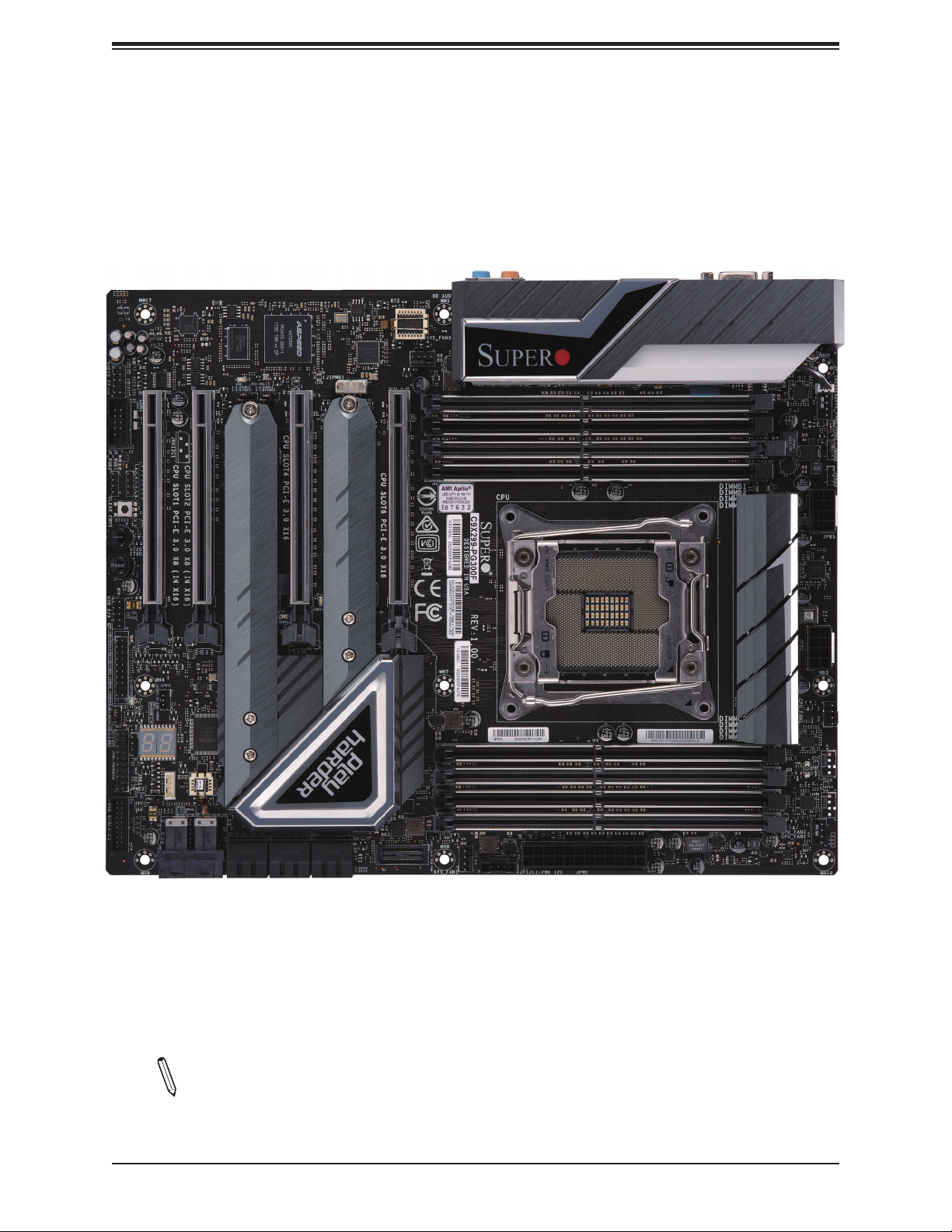
Figure 1-1. C9X299-PG300F Motherboard Image
Note: All graphics shown in this manual were based upon the latest PCB revision
available at the time of publication of the manual. The motherboard you received may
or may not look exactly the same as the graphics shown in this manual.
8
Page 9
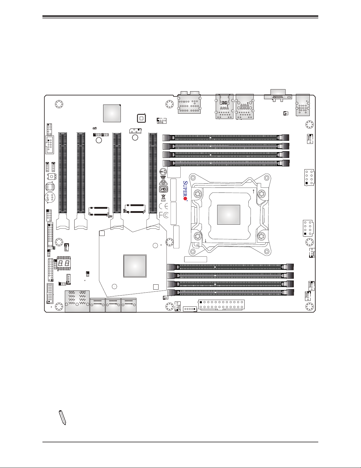
Chapter 1: Introduction
JP_RGB2
CLEAR CMOS
AUDIO_FP
COM1
JP_RGB1
CPU SLOT1 PCI-E 3.0 X8 (IN X16)
Power
Button
Reset
Button
USB 2/3
Figure 1-2. C9X299-PG300F Motherboard Layout
A C
JPG1:VGA
JPB1
CPU SLOT2 PCI-E 3.0 X8 (IN X16)
PCI-E M.2-M1
C
LED6904
BMC
JIPMB1
CPU SLOT4 PCI-E 3.0 X16
PCI-E M.2-M2
A
C
LED6903
A
LAN CTRL
CPU SLOT6 PCI-E 3.0 X16
(not drawn to scale)
SYS_FAN3
BIOS
LICENSE
MAC CODE
BAR CODE
HD AUDIO
C9X299-PG300F REV:1.01
DESIGNED IN USA
MAC CODE
LAN2 LAN1
USB3.0 (3.1 Gen1) 4/5USB3.1 (3.1 Gen2) 6/7
CPU
OPEN 1st
VGA
BT1
DIMMB1
DIMMB2
DIMMA1
DIMMA2
KB/Mouse
USB 0/1
JPW2
SYS_FAN2
JPW3
JF1
LED7201
C
A
JWD1
JTPM1:TPM/PORT80
JD1
RAID KEY-1
USB3.0 (3.1 Gen1) 8/9
JPME2
JSTBY1
LED1
JRK1
U.2-1
U.2-2
JL1
I-SATA4
I-SATA5
I-SATA2
I-SATA3
I-SATA0
I-SATA1
PCH
1
JSD1:SATA DOM PWR
SYS_FAN1
JPI2C1:PWR I2C
IPMI CODE
JPW1
CLOSE 1st
CPU_FAN1
12V_PUMP_PWR1
DIMMC2
DIMMC1
DIMMD2
DIMMD1
CPU_FAN2
24
Note: Components not documented are for internal testing only.
9
Page 10
Super C9X299-PG300F User's Manual
JPG1
JPB1
BMC
AUDIO_FP
COM1
JP_RGB1
JP_RGB2
CLEAR CMOS
Power Button
PCI-E M.2-M2
PCI-E M.2-M1
Reset Button
LED6903
USB 2/3
LED6904
JF1
LED7201
JSTBY1
JWD1
JD1
JTPM1
JRK1
JPME2
USB 3.0
(3.1 Gen1)
8/9
AUDIO_FP
COM1
JP_RGB1
JP_RGB2
CLEAR CMOS
Power
Button
Reset
Button
USB 2/3
JF1
LED7201
C
A
JWD1
JTPM1:TPM/PORT80
JD1
RAID KEY-1
USB3.0 (3.1 Gen1) 8/9
LED1
CPU SLOT1 PCI-E 3.0 X8 (IN X16)
JSTBY1
LED1
JRK1
JPME2
U.2-1
U.2-2
A C
JPG1:VGA
JPB1
CPU SLOT2 PCI-E 3.0 X8 (IN X16)
PCI-E M.2-M1
JL1
I-SATA4
U.2-1
I-SATA5
U.2-2
I-SATA2~3
I-SATA4~5
CPU SLOT4 PCI-E 3.0 X16
A
C
LED6904
I-SATA2
I-SATA3
I-SATA0~1
JIPMB1
PCI-E M.2-M2
A
C
LED6903
I-SATA0
I-SATA1
Quick Reference
LAN2
USB 3.1 (3.1 Gen2) 6/7
SYS_FAN3
LAN CTRL
JIPMB1
CPU SLOT6 PCI-E 3.0 X16
PCH
JSD1:SATA DOM PWR
HD AUDIO
SYS_FAN3
BIOS
LICENSE
MAC CODE
DESIGNED IN USA
BAR CODE
MAC CODE
1
SYS_FAN1
JSD1
SYS_FAN1
HD AUDIO
C9X299-PG300F REV:1.01
JPI2C1:PWR I2C
IPMI CODE
JPI2C1
JPW1
CLOSE 1st
JPW1JL1
LAN1
USB 3.0 (3.1 Gen1) 4/5
LAN2 LAN1
USB3.0 (3.1 Gen1) 4/5USB3.1 (3.1 Gen2) 6/7
OPEN 1st
CPU
24
VGA
VGA
BT1
DIMMB1
DIMMB2
DIMMA1
DIMMA2
KB/Mouse
USB 0/1
KB/Mouse
USB 0/1
SYS_FAN2
JPW3
JPW2
CPU_FAN1
12V_PUMP_PWR1
DIMMC2
DIMMC1
DIMMD2
DIMMD1
CPU_FAN2
BT1
DIMMB1
SYS_FAN2
DIMMB2
DIMMA1
DIMMA2
JPW3
JPW2
CPU_FAN1
DIMMC2
DIMMC1
DIMMD2
12V_PUMP_PWR1
DIMMD1
CPU_FAN2
Notes:
• See Chapter 2 for detailed information on jumpers, I/O ports, and JF1 front panel connec-
tions. Jumpers/LED indicators not indicated are used for testing only.
• " " indicates the location of Pin 1.
• When LED7201 (Onboard Power LED indicator) is on, system power is on. Unplug the
power cable before installing or removing any components.
10
Page 11

Chapter 1: Introduction
Quick Reference Table
Jumper Description Default Setting
CLEAR CMOS CMOS Clear Switch Push Button Switch
JPB1 IPMI Function
JPG1 VGA Enable/Disable Pins 1-2 (Enable)
JPME2 Intel Manufacturing Mode Pins 1-2 (Normal)
JWD1 Watch Dog Function Enable Pins 1-2 (RST)
POWER BUTTON Internal Power Button Push Button Switch
RESET BUTTON Onboard System Reset Button Push Button Switch
LED Description Status
LED1 Status Code LED Digital Readout
LED6903 M.2 Connector 2 SSD Active LED Activity: Green Blinking
LED6904 M.2 Connector 1 SSD Active LED Activity: Green Blinking
LED7201 Onboard Standby PWR LED Power On: Green On
Pins 1-2 (Enabled)
Pins 2-3 (Disable)
Connector Description
12V_PUMP_PWR1 12V 4-pin power connector for CPU liquid cooling pump
AUDIO_FP Front Panel Audio Header
BT1 Onboard Battery Header
COM1 COM1 Header
CPU_FAN1, CPU_FAN2 CPU Fan Headers
CPU SLOT 1/2 PCI-E 3.0 x8 (IN x16) PCI-E x16 Slots (PCI-E 3.0 x8 link)
CPU SLOT 4/6 PCI-E 3.0 x16 PCI-E x16 Slots (PCI-E 3.0 x16 link)
HD AUDIO High Denition Audio Header
I-SATA0~5 (Intel X299) Serial ATA (SATA 3.0) Ports 0~5 (6Gb/sec)
JD1 Speaker Header (Pins 1-4: Speaker)
JF1 Front Control Panel Header
JIPMB1 4-pin External I2C Header (for an IPMI card)
JL1 Chassis Intrusion Header
JPI2C1 Power Supply SMBus I2C Header
JP_RGB1, JP_RGB2 LED Light Bar Headers
JPW1 24-pin ATX Main Power Connector (Required)
JPW2, JPW3 +12V 8-pin CPU Power Connectors (Required)
JRK1 Intel RAID Key Header
JSD1 SATA Disk-On-Module (DOM) Power Connector
JSTBY1 Standby Power Header
Note: The table above is continued on the next page.
11
Page 12

Super C9X299-PG300F User's Manual
Connector Description
JTPM1 Trusted Platform Module (TPM)/Port 80 Header
KB/MOUSE PS/2 Keyboard/Mouse Port
LAN1, LAN2 LAN1: 10Gb LAN Port, LAN2: 1Gb LAN Port
PCI-E M.2-M1, PCI-E M.2-M2 PCI-E M.2 Connectors 1 and 2 (Small form factor devices and other portable devices
for high speed SSDs)
SYS_FAN1/2/3 System Fan Headers
U.2-1, U.2-2 U.2 Connector 1 and 2 for 2.5" NVME SSD Drives
USB 0/1 Back Panel USB 2.0 Ports
USB 2/3 Front Access USB 2.0 Header
USB 4/5 Back Panel USB 3.1 Gen1 Ports
USB 6/7 Back Panel USB 3.1 Gen2 Ports (USB6: Type A, USB7: Type C)
USB 8/9 Front Panel USB 3.1 Gen1 Header
12
Page 13
Chapter 1: Introduction
Motherboard Features
Motherboard Features
CPU
•
The C9X299-PG300F motherboard supports a single Intel Core X-Series processor in an LGA2066 socket.
Memory
•
Supports up to 128GB of unbuffered Non-ECC DDR4 memory, two DIMMs per channel (2DPC) with speeds of up to
2400MHz~4000MHz (overclocked)
DIMM Size
• 4GB, 8GB, 16GB at 1.2V
Note 1: Memory speed support depends on the processor used in the system.
Note 2: For the latest CPU/memory updates, please refer to our website at http://www.supermicro.com/products/
motherboard.
Chipset
•
Intel PCH X299
Expansion Slots
•
Four (4) PCI-E 3.0 x16 slots
• Two (2) M.2 PCI-E 3.0 x4 slots (2280 x2)
• Two (2) U.2 slots
Network
•
Intel I210AT
• Aquantia AQC 107
Audio
•
Realtek ALC1220 - HD Audio 7.1
• One (1) Front Panel Audio Header
• One (1) S/PDIF Out on the rear side of the chassis
I/O Devices
Serial (COM) Header • One (1) front accessible serial header (COM1)
•
• SATA 3.0 • Six (6) I-SATA 3.0 ports (I-SATA0 ~ 5)
• RAID PCH • RAID 0, 1, 5, and 10
Peripheral Devices
• One (1) USB 3.1 Gen2 Type C port on the I/O back panel
• One (1) USB 3.1 Gen2 Type A port on the I/O back panel
• Two (2) USB 3.1 Gen1 ports on the I/O back panel
• Two (2) front accessible USB 3.1 Gen1 connections via one header
• Two (2) USB 2.0 ports on the I/O back panel
• Two (2) front accessible USB 2.0 connections via one header
Note: The table above is continued on the next page.
13
Page 14
Super C9X299-PG300F User's Manual
Motherboard Features
BIOS
•
128Mb AMI BIOS® SPI Flash BIOS
• PCI-E 3.0, ACPI 3.0, BIOS rescue hot-key, Overclock support
Power Management
•
ACPI power management
• Power button override mechanism
• Power-on mode for AC power recovery
System Health Monitoring
•
Onboard voltage monitors for CPU cores, +3.3V, +5V, +/-12V, +3.3V Stby, +5V Stby, VBAT, Memory, PCH temperature,
System temperature, and Memory temperature
• CPU 8 phase-switching voltage regulator
• CPU/System overheat control
• CPU Thermal Trip support
Fan Control
•
Five (5) proprietary 4-pin fan headers
• Fan status monitoring via IPMI connections
• Dual cooling zone
• Multi-speed fan control via onboard BMC
• Pulse Width Modulation (PWM) fan control
System Management
•
PECI (Platform Environment Control Interface) 3.1 support
• SuperDoctor® 5, Watch Dog, NMI
• Chassis Intrusion header and detection
• Power supply monitoring
LED Indicators
CPU/System overheat LED
•
• Power LED
• Fan failed LED
• HDD activity LED
• LAN activity LED
Other
•
RoHS
Dimensions
•
ATX form factor (12.0" x 9.6") (304.80 mm x 243.84 mm)
Note 1: The CPU maximum thermal design power (TDP) is subject to chassis and
heatsink cooling restrictions. For proper thermal management, please check the chas-
sis and heatsink specications for proper CPU TDP sizing.
14
Page 15
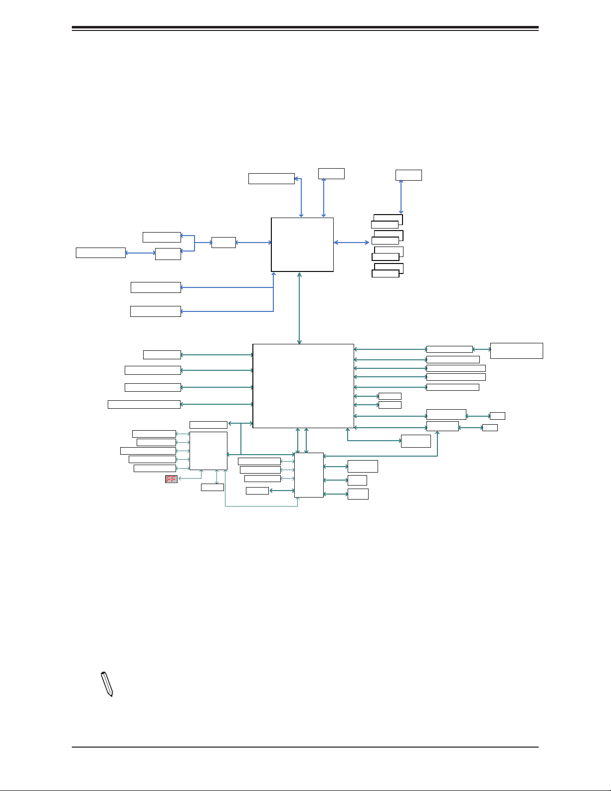
Figure 1-3.
Chipset Block Diagram (28 Lanes)
Chapter 1: Introduction
PCI-E x16 SLOT2
USB3.1 Type A+Type C
PCI-E 3.0 x4
SWITCH
PCI-E x16 SLOT4
PCI-E x16 SLOT6
6X SATA-III
M.2 SOCKET SSD
M.2 SOCKET SSD
COM1 Header
PS2 KB/MS
FAN SPEED CTRL
Voltage monitor
Temp Sensor
SWITCH
PCI-E 3.0 x16
SATA-III
6Gb/s
PCI-E 3.0 x4
8GT/s
PCI-E 3.0 x4
8GT/s
PCI-E 3.0 x2
8GT/s
TPM Header
NCT6792D-B
LPC I/O
SMBUS
PCH
PCI-E 3.0 x8
8.0GT/s
8.0GT/s
SKX-X : VR13
PCI-E 3.0 x4
8.0GT/s
LPC
FAN SPEED CTRL
Voltage monitor
Te
mp Sensor
SMBUS
SVID
Intel
PCI-E-28 Lanes
(Socket-R)
x4 DMI
8GT/s
Intel
PCH
USB 2.0 x2
PCI-E 3.0 x1
AST2500
SMBUS
SMBUS
RMII
DDR4 (2DPC)
Non-ECC UDIMM
DIMMA1
DIMMB1
DIMMC1
DIMMD1
AZALIA
USB3.0
5Gbps
USB2.0
480Mbps
PCI-E 3.0 x2
PCI-E 3.0 x1
FLASH
SPI 128Mb
VGA
DDR4
DIMMA0
DIMMB0
DIMMC0
DIMMD0
USB3.0
5Gbps
USB2.0
480Mbps
GPIO
SMBUS
8GT/s
8GT/s
SMBUS
FLASH
SPI 128Mb
Realtek ALC1220
2 X USB 3.0 Rear
2 X USB 3.0 Header
2 X USB 2.0 Header
2 X USB 2.0 Rear
GLAN
AQC107-B1-C
GLAN
WGI210AT
Share LAN
Audio Jack/
Audio Pin Header
RJ45
RJ45
Note: This is a general block diagram and may not exactly represent the features on
your motherboard. See the previous pages for the actual specications of your motherboard.
15
Page 16

Super C9X299-PG300F User's Manual
Chipset Block Diagram (44 Lanes)
Figure 1-3.
PCI-E x16 SLOT2
USB3.1 Type A+Type C
PCI-E x16 SLOT1
PCI-E 3.0 x4
PCI-E 3.0 x4
PCI-E 3.0 x8
SWITCH
PCI-E x16 SLOT4
PCI-E x16 SLOT6
6X SATA-III
M.2 SOCKET SSD
M.2 SOCKET SSD
COM1 Header
PS2 KB/MS
FAN SPEED CTRL
Voltage monitor
Temp Sensor
PCI-E 3.0 x8
PCI-E 3.0 x4
PCI-E 3.0 x8
TPM Header
NCT6792D-B
SWITCH
SWITCH
SWITCH
PCI-E 3.0 x8
8.0GT/s
PCI-E 3.0 x8
8.0GT/s
SATA-III
6Gb/s
PCI-E 3.0 x4
8GT/s
PCI-E 3.0 x4
8GT/s
PCI-E 3.0 x2
8GT/s
LPC I/O
SMBUS
PCH
SKX-X : VR13
PCI-E 3.0 x8
8.0GT/s
PCI-E 3.0 x4
8.0GT/s
PCI-E 3.0 x8
8.0GT/s
LPC
FAN SPEED CTRL
Voltage monitor
Temp Sensor
SMBUS
SVID
Intel
PCI-E-44 Lanes
(Socket-R)
x4 DMI
8GT/s
Intel
PCH
USB2.0 x2
PCI-E 3.0 x1
AST2500
SMBUS
SMBUS
RMII
DDR4 (2DPC)
Non-ECC UDIMM
DIMMA0
DIMMA1
DIMMB0
DIMMB1
DIMMC0
DIMMC1
DIMMD0
DIMMD1
AZALIA
USB3.0
5Gbps
USB2.0
480Mbps
PCI-E 3.0 x1
8GT/s
FLASH
SPI 128Mb
VGA
DDR4
USB3.0
USB2.0
480Mbps
GPIO
SMBUS
SMBUS
5Gbps
PCI-E 3.0 x2
8GT/s
FLASH
SPI
128Mb
Realtek ALC1220
2 X USB 3.0 Rear
2 X USB 3.0 Header
2 X USB 2.0 Header
2 X USB 2.0 Rear
GLAN
AQC107-B1-C
GLAN
WGI210AT
Audio Jack/
Audio Pin Header
RJ45
RJ45
Note: This is a general block diagram and may not exactly represent the features on
your motherboard. See the previous pages for the actual specications of your motherboard.
16
Page 17

Chapter 1: Introduction
1.2 Processor and Chipset Overview
The C9X299-PG300F supports an Intel Core X-Series processor in the LGA2066 socket. With
the Intel X299 PCH, the C9X299-PG300F is a high-end, multi-GPU motherboard that offers
reliability and stability. It offers the latest high-performance features such as NVMe, M.2/U.2
storage interfaces, and DDR4 memory with speeds of up to 4000MHz (OC).
The C9X299-PG300F supports the following features:
• ACPI Power Management Logic Support Rev. 4.0a
• Intel Turbo Boost Technology
• Congurable TDP (cTDP) and Lower-Power Mode
• Adaptive Thermal Management/Monitoring
• PCI-E 3.0, SATA 3.0, NVMe, U.2 and M.2 connectors
• System Management Bus (SMBus) Specication Version 2.0
• Intel Trusted Execution Technology (Intel TXT)
• Intel Rapid Storage Technology
• Intel Virtualization Technology for Directed I/O (Intel VT-d)
1.3 Special Features
This section describes the health monitoring features of the C9X299-PG300F motherboard.
The motherboard has an onboard System Hardware Monitor chip that supports system health
monitoring.
Recovery from AC Power Loss
The Basic I/O System (BIOS) provides a setting that determines how the system will respond
when AC power is lost and then restored to the system. You can choose for the system to
remain powered off (in which case you must press the power switch to turn it back on), or
for it to automatically return to the power-on state. See the Advanced BIOS Setup section
for this setting. The default setting is Last State.
17
Page 18

Super C9X299-PG300F User's Manual
1.4 System Health Monitoring
The motherboard has an onboard Baseboard Management Controller (BMC) chip that
supports system health monitoring.
Onboard Voltage Monitors
The onboard voltage monitor will continuously scan crucial voltage levels. Once a voltage
becomes unstable, it will give a warning or send an error message to the screen. Users can
adjust the voltage thresholds to dene the sensitivity of the voltage monitor. Real time readings
of these voltage levels are all displayed in the BIOS.
Fan Status Monitor with Firmware Control
The system health monitor embedded in the BMC chip can check the RPM status of the
cooling fans. The CPU and chassis fans are controlled via IPMI.
Environmental Temperature Control
System Health sensors in the BMC monitor the temperatures and voltage settings of onboard
processors and the system in real time via the IPMI interface. Whenever the temperature of
the CPU or the system exceeds a user-dened threshold, system/CPU cooling fans will be
turned on to prevent the CPU or the system from overheating
Note: To avoid possible system overheating, please be sure to provide adequate air-
ow to your system.
System Resource Alert
This feature is available when used with SuperDoctor 5 in the Windows OS or in the Linux
environment. SuperDoctor is used to notify the user of certain system events. For example,
you can congure SuperDoctor to provide you with warnings when the system temperature,
CPU temperatures, voltages, and fan speeds go beyond a predened range.
1.5 ACPI Features
ACPI stands for Advanced Conguration and Power Interface. The ACPI specication denes
a exible and abstract hardware interface that provides a standard way to integrate power
management features throughout a computer system, including its hardware, operating
system, and application software. This enables the system to automatically turn on and off
peripherals such as CD-ROMs, network cards, hard disk drives, and printers.
18
Page 19

Chapter 1: Introduction
In addition to enabling operating system-directed power management, ACPI also provides a
generic system event mechanism for Plug and Play, and an operating system-independent
interface for conguration control. ACPI leverages the Plug and Play BIOS data structures,
while providing a processor architecture-independent implementation that is compatible with
Windows® 7, Windows 8, and Windows 2012 Operating Systems.
1.6 Power Supply
As with all computer products, a stable power source is necessary for proper and reliable
operation. It is even more important for processors that have high CPU clock rates.
The C9X299-PG300F motherboard accommodates a 24-pin ATX power supply. Although most
power supplies generally meet the specications required by the CPU, some are inadequate.
In addition, a 12V 8-pin power connection is also required to ensure adequate power supply
to the system.
Warning: To prevent damage to the power supply or the motherboard, use power
supplies that contain 24-pin and 8-pin power connectors. Connect the power supplies
to the 24-pin (JPW1) and the 8-pin power connectors (JPW2/JPW3) on the motherboard. Failure in doing so may void the manufacturer warranty on your power supply
and motherboard.
It is strongly recommended that you use a high quality power supply that meets ATX power
supply Specication 2.02 or above. It must also be SSI compliant. For more information,
please refer to the website at http://www.ssiforum.org/. Additionally, in areas where noisy
power transmission is present, you may choose to install a line lter to shield the computer
from noises. It is recommended that you also install a power surge protector to help avoid
problems caused by power surges.
1.7 Serial Port
The C9X299-PG300F motherboard supports one serial communication connection. COM1
header can be used for input/output. The UART provides legacy speeds with a baud rate of
up to 115.2 Kbps as well as an advanced speed with baud rates of 250 K, 500 K, or 1 Mb/s,
which support high-speed serial communication devices.
19
Page 20

Super C9X299-PG300F User's Manual
Chapter 2
Installation
2.1 Static-Sensitive Devices
Electrostatic Discharge (ESD) can damage electronic com ponents. To prevent damage to your
motherboard, it is important to handle it very carefully. The following measures are generally
sufcient to protect your equipment from ESD.
Precautions
• Use a grounded wrist strap designed to prevent static discharge.
• Touch a grounded metal object before removing the board from the antistatic bag.
• Handle the board by its edges only; do not touch its components, peripheral chips, memory
modules or gold contacts.
• When handling chips or modules, avoid touching their pins.
• Put the motherboard and peripherals back into their antistatic bags when not in use.
• For grounding purposes, make sure your computer chassis provides excellent conductivity
between the power supply, the case, the mounting fasteners, and the motherboard.
• Use only the correct type of onboard CMOS battery. Do not install the onboard battery
upside down to avoid possible explosion.
Unpacking
The motherboard is shipped in antistatic packaging to avoid static damage. When unpacking
the motherboard, make sure that the person handling it is static protected.
20
Page 21
Chapter 2: Installation
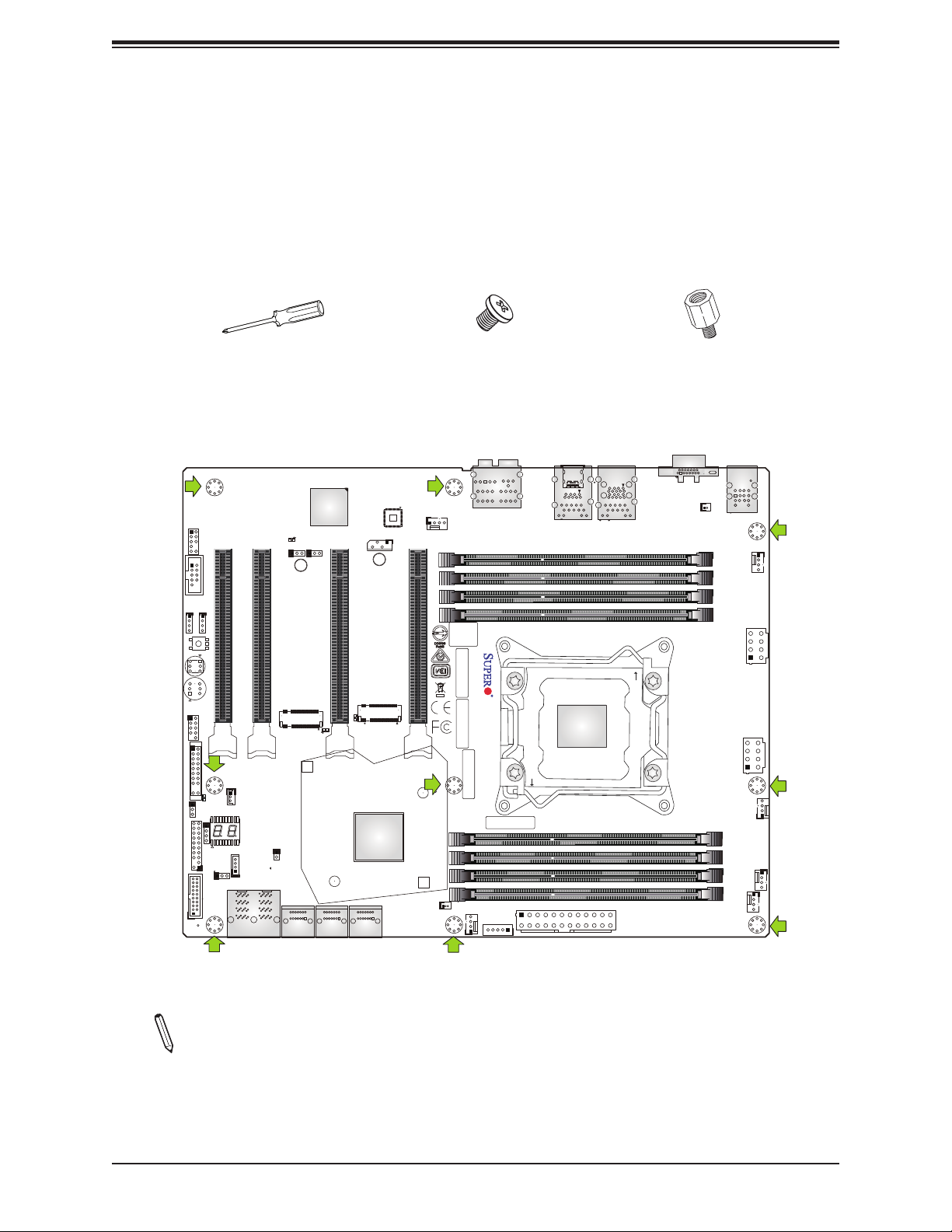
2.2 Motherboard Installation
All motherboards have standard mounting holes to t different types of chassis. Make sure
that the locations of all the mounting holes for both the motherboard and the chassis match.
Although a chassis may have both plastic and metal mounting fasteners, metal ones are
highly recommended because they ground the motherboard to the chassis. Make sure that
the metal standoffs click in or are screwed in tightly.
Phillips Screwdriver (1)
Tools Needed
AUDIO_FP
COM1
JP_RGB1
JP_RGB2
CLEAR CMOS
Button
Button
USB 2/3
JF1
LED7201
C
A
JWD1
JTPM1:TPM/PORT80
JD1
RAID KEY-1
USB3.0 (3.1 Gen1) 8/9
CPU SLOT1 PCI-E 3.0 X8 (IN X16)
Power
Reset
JSTBY1
LED1
JPME2
A C
JPG1:VGA
JPB1
CPU SLOT2 PCI-E 3.0 X8 (IN X16)
PCI-E M.2-M1
JL1
JRK1
I-SATA4
U.2-1
I-SATA5
U.2-2
C
LED6904
BMC
JIPMB1
CPU SLOT4 PCI-E 3.0 X16
PCI-E M.2-M2
A
C
LED6903
A
PCH
I-SATA0
I-SATA2
I-SATA1
I-SATA3
Phillips Screws (9)
LAN CTRL
SYS_FAN3
CPU SLOT6 PCI-E 3.0 X16
BIOS
LICENSE
C9X299-PG300F REV:1.01
MAC CODE
DESIGNED IN USA
BAR CODE
MAC CODE
1
JSD1:SATA DOM PWR
SYS_FAN1
JPI2C1:PWR I2C
HD AUDIO
IPMI CODE
JPW1
CLOSE 1st
LAN2 LAN1
USB3.0 (3.1 Gen1) 4/5USB3.1 (3.1 Gen2) 6/7
CPU
Standoffs (9)
Only if Needed
VGA
OPEN 1st
24
BT1
DIMMB1
DIMMB2
DIMMA1
DIMMA2
DIMMC2
DIMMC1
DIMMD2
DIMMD1
KB/Mouse
USB 0/1
JPW2
CPU_FAN2
SYS_FAN2
JPW3
CPU_FAN1
12V_PUMP_PWR1
Location of Mounting Holes
Notes: 1. To avoid damaging the motherboard and its components, please do not use
a force greater than 8 lb/inch on each mounting screw during motherboard installation.
2. Some components are very close to the mounting holes. Please take precautionary
measures to avoid damaging these components when installing the motherboard to
the chassis.
21
Page 22
Super C9X299-PG300F User's Manual
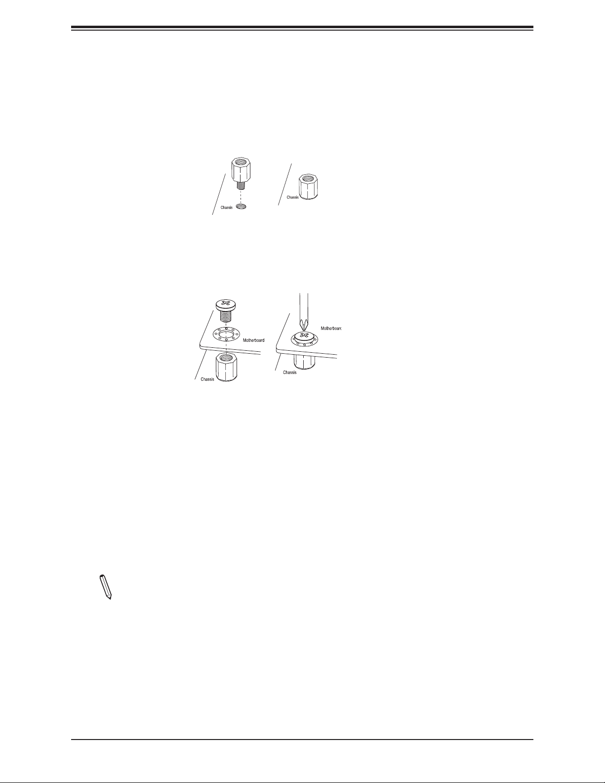
Installing the Motherboard
1. Locate the mounting holes on the motherboard. See the previous page for the location.
2. Locate the matching mounting holes on the chassis. Align the mounting holes on the
motherboard against the mounting holes on the chassis.
3. Install standoffs in the chassis as needed.
4. Install the motherboard into the chassis carefully to avoid damaging other motherboard
components.
5. Using the Phillips screwdriver, insert a Phillips head #6 screw into a mounting hole on
the motherboard and its matching mounting hole on the chassis.
6. Repeat Step 5 to insert remaining screws into all mounting holes.
7. Make sure that the motherboard is securely placed in the chassis.
Note: Images displayed are for illustration only. Your chassis or components might
look different from those shown in this manual.
22
Page 23

Chapter 2: Installation
2.3 Installing an M.2 Device (optional)
Two M.2 (M-key) connectors are supported by the C9X299-PG300F. M.2 devices are used
for solid state storage and internal expansion. Follow the steps below in order to install an
M.2 device.
Note: A screwdriver will be required.
1. Locate and remove the retaining screws on the M.2 heatsink.
2. With the heatsink removed, locate the appropriate standoff for the M.2 card's length.
3. Remove the associated standoff screw and set it aside.
4. Carefully plug the M.2 device into the M.2 connector and lower the semi-circle notched
end onto the standoff.
5. Replace the standoff screw and tighten it to secure the M.2 device into place. Do not
overtighten so as to avoid damaging the M.2 device.
6. Replace the M.2 heatsink and the retaining screws. Tighten the screws to secure the
heatsink into place.
23
Page 24
Super C9X299-PG300F User's Manual
2.4 Processor and Heatsink Installation
Warning: When handling the processor package, avoid placing direct pressure on the label
area of the fan.
Important:
• Always connect the power cord last, and always remove it before adding, removing, or
changing any hardware components. Make sure that you install the processor into the CPU
socket before you install the CPU heatsink.
• If you buy a CPU separately, make sure that you use an Intel-certied multi-directional
heatsink only.
• Make sure to install the motherboard into the chassis before you install the CPU heatsink.
• When receiving a motherboard without a processor pre-installed, make sure that the plastic
CPU socket cap is in place and none of the socket pins are bent; otherwise, contact your
retailer immediately.
• Refer to the Supermicro website for updates on CPU support.
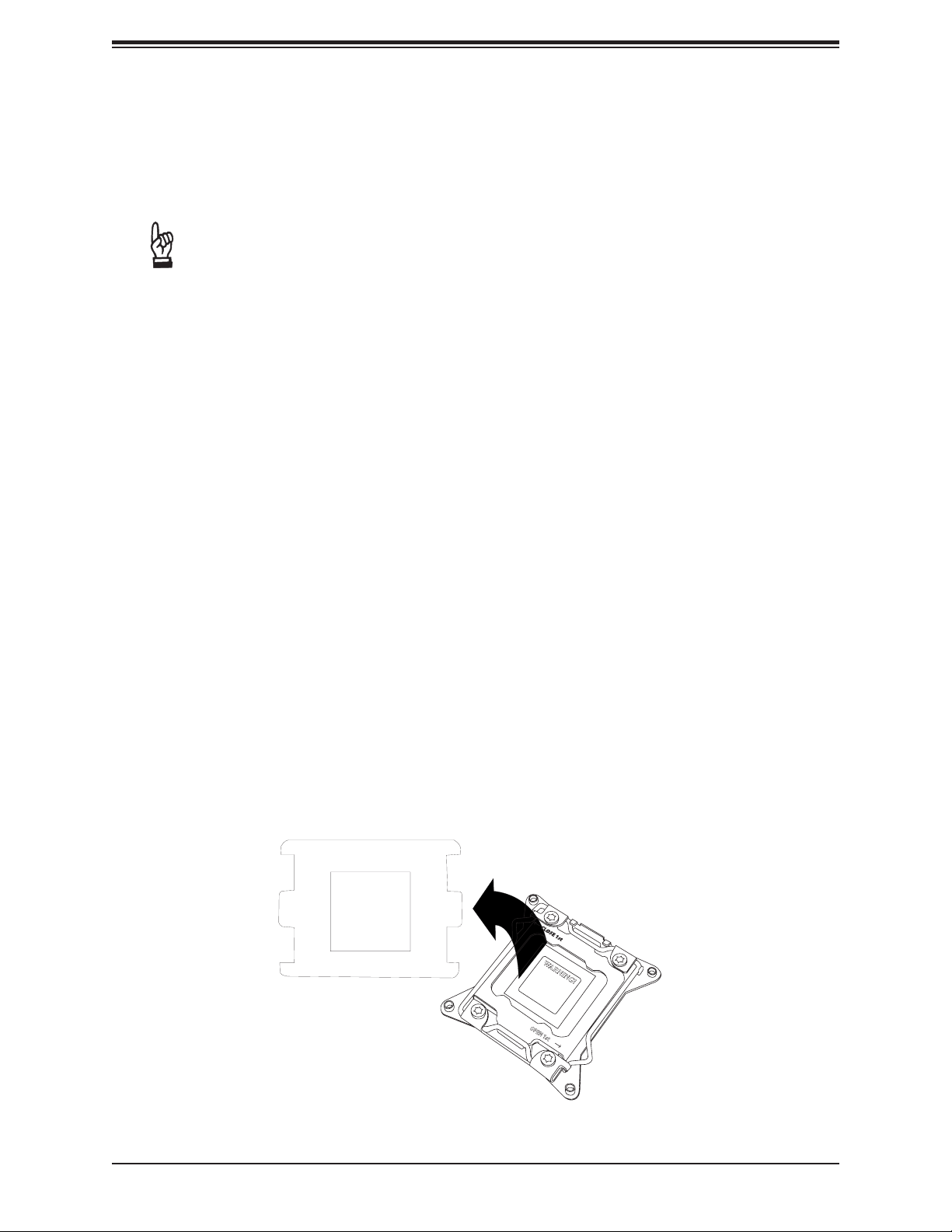
Installing a CPU
1. Remove the WARNING plastic cap from the socket.
WARNING!
24
WARNING!
OPEN 1st
Page 25
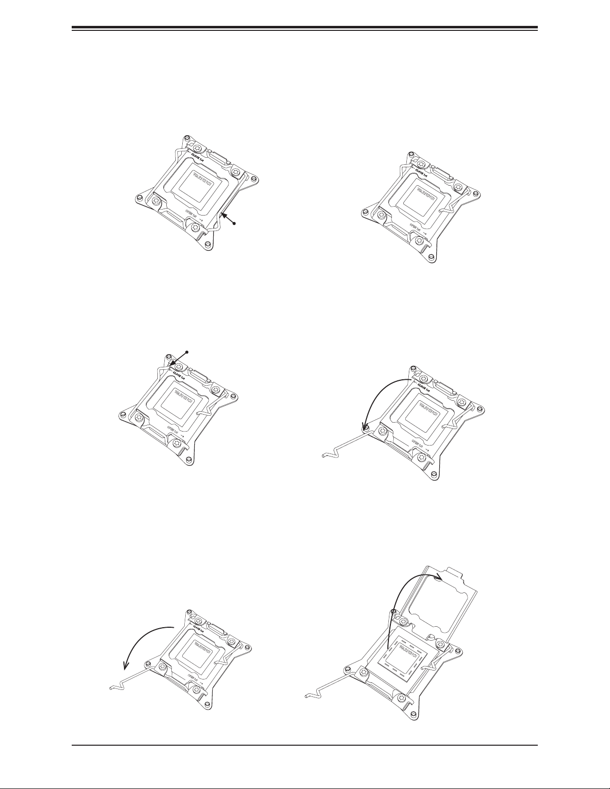
Chapter 2: Installation
2. There are two load levers on the LGA2066 socket. To open the socket cover, press and
release the "Unlock 1st" lever, marked by an unlock symbol.
1
WARNING!
OPEN 1st
Press down on
2
WARNING!
OPEN 1st
Load Lever labeled
'Open 1st'.
3. Press the "Lock 1st" lever, marked by a lock symbol, to release the load plate that
covers the CPU socket from its locking position.
Press down on
1
Lever 'Close 1st'
WARNING!
OPEN 1st
Load
Pull the lever away
2
from the socket
WARNING!
OPEN 1st
4. With the "Lock 1st" lever fully retracted, gently push down on the "Unlock 1st" lever to
open the load plate. Lift the load plate to open it completely.
Gently push down
1
to pop the load plate
open.
WARNING!
OPEN 1st
2
WARNING!
25
Page 26
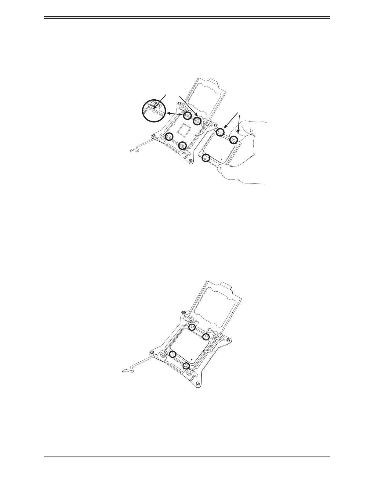
Super C9X299-PG300F User's Manual
5. Use your thumb and index nger to hold the CPU on its edges. Align the CPU keys,
which have semi-circle cutouts, against the socket keys.
Socket Keys
CPU Keys
6. Once they are aligned, carefully lower the CPU straight down into the socket. To avoid
damaging the CPU or socket, do not drop the CPU onto the socket, move it horizontally
or vertically, or rub it against the socket pins.
7. With the CPU inside the socket, inspect the four corners of the CPU to make sure that it
is properly installed.
26
Page 27
Chapter 2: Installation
8. Close the load plate with the CPU inside the socket. Lock the "Lock 1st" lever rst, then
lock the "Unlock 1st" lever second. Gently push the load levers down to the lever locks.
Gently close the
1
3
load plate.
Lever Lock
Push down and
lock 'Open 1st'
lever
Push down and lock
2
'Close 1st' lever.
OPEN 1st
4
OPEN 1st
OPEN 1st
Lever Lock
27
Page 28
Super C9X299-PG300F User's Manual
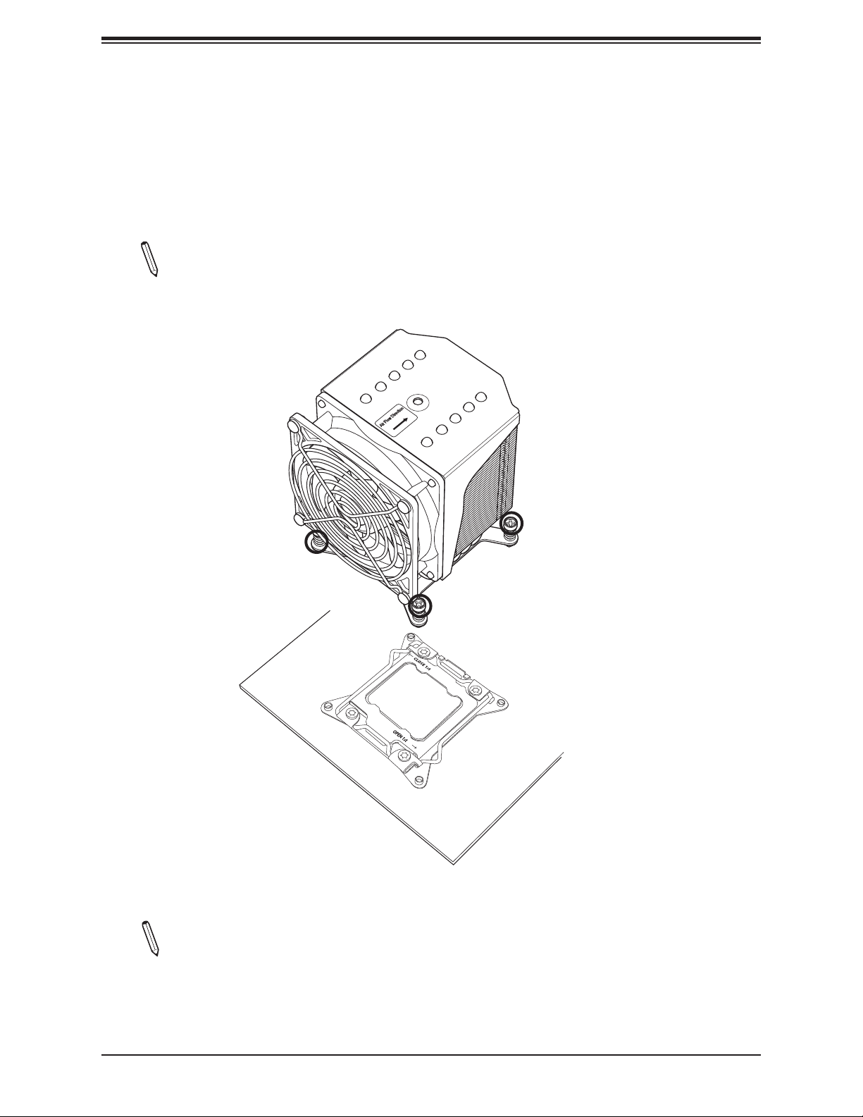
Installing a CPU Heatsink
1. Apply the proper amount of thermal grease to the heatsink.
2. Place the heatsink on top of the CPU so that the four mounting holes on the heatsink
are aligned with those on the retention mechanism. Tighten the screws in the following
order:
Note: Screw #1 is not shown in the illustration. It is found opposite of Screw #2.
Screw #3
Screw #4
Screw #2
Note: Graphic drawings included in this manual are for reference only. They might look
different from the components installed in your system.
28
Page 29
Chapter 2: Installation
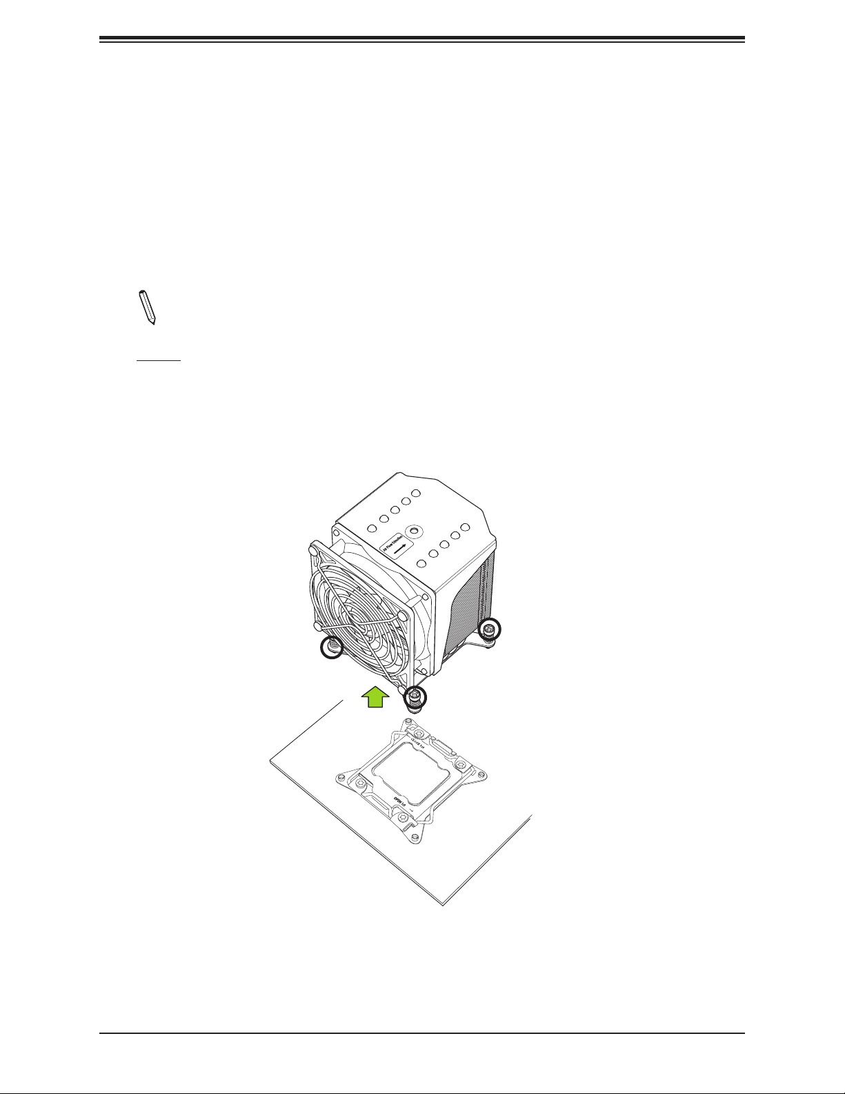
Removing a Heatsink
Warning: We do not recommend that the CPU or the heatsink be removed. However, if you
do need to remove the heatsink, please follow the instructions below to uninstall the heatsink
to avoid damaging the CPU or other components.
1. Unplug the power cord from the power supply.
2. Loosen the screws in the order below.
Note: Screw #1 is not shown in the illustration. It is found opposite of Screw #2.
3. Gently wiggle the heatsink to loosen it. Do not use excessive force when wiggling the
heatsink.
4. Once the heatsink is loosened, remove it from the motherboard.
Screw #4
Screw #3
Screw #2
29
Page 30
Super C9X299-PG300F User's Manual
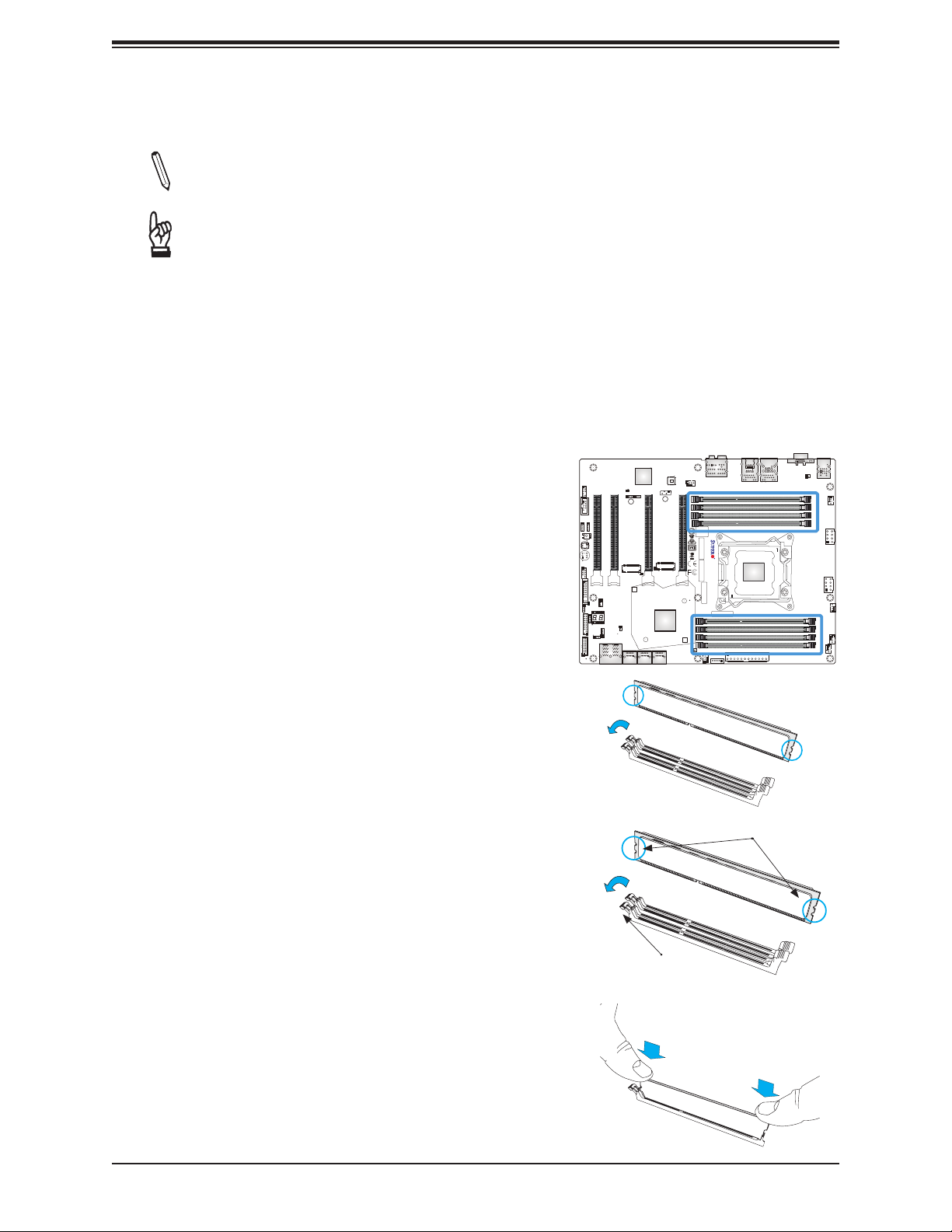
2.5 Memory Support and Installation
Note: Check the Supermicro website for recommended memory modules.
Important: Exercise extreme care when installing or removing DIMM modules to pre-
vent any possible damage.
Memory Support
The C9X299-PG300F motherboard supports up to 128GB of Non-ECC DDR4 memory with
speeds of up to 4000MHz (overclocked) in eight memory slots. Populating these DIMM slots
with memory modules of the same type and size will result in interleaved memory, which will
improve memory performance.
DIMM Installation
1. Insert the desired number of DIMMs into the
memory slots, starting with DIMMA1, DIMMB1,
DIMMC1, DIMMD1, then DIMMA2, DIMMB2,
DIMMC2, DIMMD2. For best performance,
please use the memory modules of the same
type and speed.
2. Push the release tabs outwards on both ends
of the DIMM slot to unlock it.
3. Align the key of the DIMM module with the
receptive point on the memory slot.
4. Align the notches on both ends of the module
against the receptive points on the ends of the
slot.
5. Use two thumbs together to press the notches
on both ends of the module straight down into
the slot until the module snaps into place.
JP_RGB2
CLEAR CMOS
JTPM1:TPM/PORT80
AUDIO_FP
COM1
JP_RGB1
Power
Button
Reset
Button
USB 2/3
JF1
LED7201
C
A
JWD1
JD1
RAID KEY-1
USB3.0 (3.1 Gen1) 8/9
JPME2
CPU SLOT2 PCI-E 3.0 X8 (IN X16)
CPU SLOT1 PCI-E 3.0 X8 (IN X16)
JSTBY1
LED1
JRK1
U.2-1
U.2-2
JPB1
PCI-E M.2-M1
JL1
VGA
LAN CTRL
BMC
SYS_FAN3
HD AUDIO
LAN2 LAN1
JIPMB1
A C
JPG1:VGA
CPU SLOT4 PCI-E 3.0 X16
CPU SLOT6 PCI-E 3.0 X16
BIOS
LICENSE
C9X299-PG300F REV:1.01
MAC CODE
PCI-E M.2-M2
A
C
LED6903
A
C
LED6904
I-SATA0
I-SATA4
I-SATA2
I-SATA5
I-SATA1
I-SATA3
DESIGNED IN USA
BAR CODE
MAC CODE
PCH
1
SYS_FAN1
JSD1:SATA DOM PWR
JPI2C1:PWR I2C
USB3.0 (3.1 Gen1) 4/5USB3.1 (3.1 Gen2) 6/7
CPU
CLOSE 1st
IPMI CODE
JPW1
BT1
KB/Mouse
USB 0/1
SYS_FAN2
DIMMB1
DIMMB2
DIMMA1
DIMMA2
JPW3
OPEN 1st
JPW2
CPU_FAN1
12V_PUMP_PWR1
DIMMC2
DIMMC1
DIMMD2
DIMMD1
CPU_FAN2
24
Notches
6. Press the release tabs to the lock positions to
secure the DIMM module into the slot.
DIMM Removal
Press both release tabs on the ends of the DIMM
module to unlock it. Once the DIMM module is
loosened, remove it from the memory slot.
30
Release Tab
Press down on the
stationary end rst,
then the locking end.
Page 31

Chapter 2: Installation
Memory Population Guidelines
When installing memory modules, always use DDR4 DIMM modules of the same size, type,
and speed. Mixed DIMM speeds can be installed. However, all DIMMs will run at the speed
of the slowest DIMM.
Depending on which CPU is installed, DIMMs should be installed in the following congurations
for optimized performance:
DIMMB2
DIMMB1
DIMMA2
DIMMA1
Towards the CPU
Towards the CPU
DIMMC1
DIMMC2
DIMMD1
DIMMD2
Core™
X-Series
(6-core or
above)
One
Two
Four
Six
Eight
31
Page 32

Super C9X299-PG300F User's Manual
2.6 Rear I/O Ports
See Figure 2-1 below for the locations and descriptions of the various I/O ports on the rear
of the motherboard.
VGA
BT1
KB/Mouse
USB 0/1
SYS_FAN2
DIMMB1
DIMMB2
DIMMA1
DIMMA2
JPW3
JPW2
CPU_FAN1
12V_PUMP_PWR1
DIMMC2
DIMMC1
DIMMD2
DIMMD1
CPU_FAN2
AUDIO_FP
COM1
JP_RGB1
JP_RGB2
CLEAR CMOS
Button
Button
USB 2/3
JF1
LED7201
C
A
JWD1
JTPM1:TPM/PORT80
JD1
RAID KEY-1
USB3.0 (3.1 Gen1) 8/9
CPU SLOT2 PCI-E 3.0 X8 (IN X16)
CPU SLOT1 PCI-E 3.0 X8 (IN X16)
Power
Reset
JSTBY1
LED1
JRK1
JPME2
U.2-1
U.2-2
A C
JPB1
PCI-E M.2-M1
JL1
I-SATA4
I-SATA5
BMC
JPG1:VGA
CPU SLOT4 PCI-E 3.0 X16
A
C
LED6904
I-SATA2
I-SATA3
A
C
LED6903
PCI-E M.2-M2
I-SATA0
I-SATA1
LAN CTRL
JIPMB1
PCH
SYS_FAN3
CPU SLOT6 PCI-E 3.0 X16
BIOS
LICENSE
1
JSD1:SATA DOM PWR
C9X299-PG300F REV:1.01
MAC CODE
DESIGNED IN USA
BAR CODE
MAC CODE
SYS_FAN1
HD AUDIO
IPMI CODE
JPI2C1:PWR I2C
JPW1
CLOSE 1st
LAN2 LAN1
USB3.0 (3.1 Gen1) 4/5USB3.1 (3.1 Gen2) 6/7
CPU
OPEN 1st
24
Figure 2-1. I/O Port Locations and Denitions
11
14
1
5
8
4
15
13
12
16
2
3
6
7
9
10
Rear I/O Ports
# Description # Description # Description # Description
1. PS2 KB/Mouse 5. LAN1 9. USB 3.1 Gen2 Port 6 13. SPDIF Out
2. USB 2.0 Port 0 6. USB 3.1 Gen1 Port 4 10. USB 3.1 Gen2 Port 7 14. Line In
3. USB 2.0 Port 1 7. USB 3.1 Gen1 Port 5 11. CEN/LFE Out 15. Line Out
4. VGA Connector 8. LAN2 12. Surround Out 16. Mic In
32
Page 33

Chapter 2: Installation
High Denition Audio (back panel ports)
This motherboard features a 7.1+2 Channel High Denition Audio (HDA) codec that provides
10 DAC channels. The HD Audio connections simultaneously supports multiple-streaming
7.1 sound playback with two channels of independent stereo output through the front panel
stereo out, and front, rear, center and subwoofer speaker connections. Use the advanced
software included in the CD with your motherboard to enable this function.
JP_RGB2
CLEAR CMOS
JTPM1:TPM/PORT80
JP_RGB1
USB 2/3
A
JWD1
AUDIO_FP
JF1
LED7201
JD1
COM1
CPU SLOT1 PCI-E 3.0 X8 (IN X16)
Power
Button
Reset
Button
JSTBY1
C
LED1
RAID KEY-1
JRK1
USB3.0 (3.1 Gen1) 8/9
JPME2
A C
JPG1:VGA
JPB1
CPU SLOT2 PCI-E 3.0 X8 (IN X16)
PCI-E M.2-M1
JL1
I-SATA4
U.2-1
I-SATA5
U.2-2
BMC
CPU SLOT4 PCI-E 3.0 X16
PCI-E M.2-M2
A
C
LED6903
A
C
LED6904
I-SATA0
I-SATA2
I-SATA1
I-SATA3
LAN CTRL
JIPMB1
PCH
SYS_FAN3
CPU SLOT6 PCI-E 3.0 X16
BIOS
LICENSE
1
JSD1:SATA DOM PWR
MAC CODE
DESIGNED IN USA
BAR CODE
MAC CODE
SYS_FAN1
HD AUDIO
C9X299-PG300F REV:1.01
IPMI CODE
JPI2C1:PWR I2C
1
1. HD AUDIO
JPW1
CLOSE 1st
LAN2 LAN1
USB3.0 (3.1 Gen1) 4/5USB3.1 (3.1 Gen2) 6/7
CPU
VGA
BT1
KB/Mouse
USB 0/1
SYS_FAN2
DIMMB1
DIMMB2
DIMMA1
DIMMA2
JPW3
OPEN 1st
JPW2
CPU_FAN1
12V_PUMP_PWR1
DIMMC2
DIMMC1
DIMMD2
DIMMD1
CPU_FAN2
24
33
Page 34

Super C9X299-PG300F User's Manual
Universal Serial Bus (USB) Ports
There are two USB 2.0 ports (USB0/1), two USB 3.1 Gen1 ports (USB4/5), and two USB
3.1 Gen2 ports (USB6/7) located on the I/O back panel. The motherboard also has one
front access USB 2.0 header (USB2/3). The USB8/9 header is USB 3.1 Gen1. The onboard
headers can be used to provide chassis USB access with a cable (not included).
Back Panel USB 0/1 (USB 2.0)
Pin Denitions
Pin# Denition Pin# Denition
1 +5V 5 +5V
2 USB_N 6 USB_N
3 USB_P 7 USB_P
4 Ground 8 Ground
Back Panel USB 4/5 (USB 3.1 Gen1)
Pin Denitions
Pin# Denition Pin# Denition
1 VBUS 10 Power
2 D- 11 USB_N
3 D+ 12 USB_P
4 GND 13 GND
5 Stda_SSRX- 14 USB3_RN
6 Stda_SSRX+ 15 USB3_RP
7 GND 16 GND
8 Stda_SSTX- 17 USB3_TN
9 Stda_SSTX+ 18 USB3_TP
Front Panel USB 2/3 (USB 2.0)
Pin Denitions
Pin# Denition Pin# Denition
1 +5V 2 +5V
3 USB_N 4 USB_N
5 USB_P 6 USB_P
7 Ground 8 Ground
9 Key 10 NC
12
VGA
LAN CTRL
AUDIO_FP
COM1
JP_RGB1
JP_RGB2
CLEAR CMOS
USB 2/3
Power
Button
Reset
Button
CPU SLOT2 PCI-E 3.0 X8 (IN X16)
CPU SLOT1 PCI-E 3.0 X8 (IN X16)
3
JF1
LED7201
JSTBY1
C
A
JWD1
LED1
JTPM1:TPM/PORT80
JD1
RAID KEY-1
JRK1
USB3.0 (3.1 Gen1) 8/9
JPME2
U.2-1
U.2-2
A C
JPB1
PCI-E M.2-M1
JL1
I-SATA4
I-SATA5
BMC
JPG1:VGA
CPU SLOT4 PCI-E 3.0 X16
A
C
LED6904
I-SATA2
I-SATA3
A
C
LED6903
PCI-E M.2-M2
I-SATA0
I-SATA1
JIPMB1
PCH
SYS_FAN3
CPU SLOT6 PCI-E 3.0 X16
BIOS
LICENSE
1
JSD1:SATA DOM PWR
MAC CODE
DESIGNED IN USA
BAR CODE
MAC CODE
SYS_FAN1
HD AUDIO
C9X299-PG300F REV:1.01
IPMI CODE
JPI2C1:PWR I2C
LAN2 LAN1
USB3.0 (3.1 Gen1) 4/5USB3.1 (3.1 Gen2) 6/7
CPU
CLOSE 1st
JPW1
OPEN 1st
24
BT1
KB/Mouse
USB 0/1
SYS_FAN2
DIMMB1
DIMMB2
DIMMA1
DIMMA2
JPW3
JPW2
CPU_FAN1
12V_PUMP_PWR1
DIMMC2
DIMMC1
DIMMD2
DIMMD1
CPU_FAN2
1. USB 0/1
2. USB 4/5
3. USB 2/3
34
Page 35

Universal Serial Bus (USB) Ports (Continued)
Chapter 2: Installation
Back Panel USB 6/7 (USB 3.1 Gen2)
Pin Denitions
Pin# Denition Pin# Denition
1 VBUS 19 Power
2 Stda_SSRX- 18 USB3_RN
3 Stda_SSRX+ 17 USB3_RP
4 GND 16 GND
5 Stda_SSTX- 15 USB3_TN
6 Stda_SSTX+ 14 USB3_TP
7 GND 13 GND
8 D- 12 USB3_N
9 D+ 11 USB3_P
10 x
Front Panel USB 8/9 (USB 3.1 Gen1)
Pin Denitions
Pin# Denition Pin# Denition
1 VBUS 11 D+
2 StdA_SSRX- 12 D-
3 StdA_SSRX+ 13 GND_DRAIN
4 GND 14 StdB_SSTX+
5 StdA_SSTX- 15 StdB_SSTX-
6 StdA_SSTX+ 16 Ground
7 GND_DRAIN 17 StdB_SSRX+
8 D- 18 StdB_SSRX-
9 D+ 19 VBUS
10 NC
1
VGA
LAN CTRL
AUDIO_FP
COM1
JP_RGB1
JP_RGB2
CLEAR CMOS
Button
USB 2/3
JF1
LED7201
C
A
JWD1
JTPM1:TPM/PORT80
JD1
USB3.0 (3.1 Gen1) 8/9
CPU SLOT1 PCI-E 3.0 X8 (IN X16)
Power
Reset
Button
JSTBY1
LED1
RAID KEY-1
JRK1
JPME2
CPU SLOT2 PCI-E 3.0 X8 (IN X16)
A C
JPB1
PCI-E M.2-M1
JL1
BMC
JPG1:VGA
CPU SLOT4 PCI-E 3.0 X16
A
C
LED6904
A
C
LED6903
PCI-E M.2-M2
2
I-SATA2
I-SATA3
I-SATA0
I-SATA1
I-SATA4
U.2-1
I-SATA5
U.2-2
JIPMB1
PCH
SYS_FAN3
CPU SLOT6 PCI-E 3.0 X16
BIOS
LICENSE
1
JSD1:SATA DOM PWR
C9X299-PG300F REV:1.01
MAC CODE
DESIGNED IN USA
BAR CODE
MAC CODE
SYS_FAN1
HD AUDIO
IPMI CODE
JPI2C1:PWR I2C
LAN2 LAN1
USB3.0 (3.1 Gen1) 4/5USB3.1 (3.1 Gen2) 6/7
CPU
CLOSE 1st
JPW1
OPEN 1st
24
BT1
KB/Mouse
USB 0/1
SYS_FAN2
DIMMB1
DIMMB2
DIMMA1
DIMMA2
JPW3
JPW2
CPU_FAN1
12V_PUMP_PWR1
DIMMC2
DIMMC1
DIMMD2
DIMMD1
CPU_FAN2
1. USB 6/7
2. USB 8/9
35
Page 36

Super C9X299-PG300F User's Manual
LAN Ports
The motherboard has one 10Gigabit Ethernet port (LAN1) and one 1Gigabit Ethernet port
(LAN2) on the I/O back panel. These ports accept RJ45 cables. Please refer to Section 2.10
for LAN LED information.
LAN Port
Pin Denitions
Pin# Denition Pin# Denition
1 TX_D1+ 5 BI_D3-
2 TX_D1- 6 RX_D2-
3 RX_D2+ 7 BI_D4+
4 BI_D3+ 8 BI_D4-
JP_RGB2
CLEAR CMOS
JTPM1:TPM/PORT80
JP_RGB1
USB 2/3
A
JWD1
AUDIO_FP
JF1
LED7201
COM1
CPU SLOT1 PCI-E 3.0 X8 (IN X16)
Power
Button
Reset
Button
JSTBY1
C
LED1
JD1
RAID KEY-1
JRK1
USB3.0 (3.1 Gen1) 8/9
JPME2
A C
JPG1:VGA
JPB1
CPU SLOT2 PCI-E 3.0 X8 (IN X16)
PCI-E M.2-M1
JL1
I-SATA4
U.2-1
I-SATA5
U.2-2
BMC
CPU SLOT4 PCI-E 3.0 X16
PCI-E M.2-M2
A
C
LED6903
A
C
LED6904
I-SATA0
I-SATA2
I-SATA1
I-SATA3
LAN CTRL
JIPMB1
PCH
SYS_FAN3
CPU SLOT6 PCI-E 3.0 X16
1
JSD1:SATA DOM PWR
BIOS
LICENSE
MAC CODE
BAR CODE
C9X299-PG300F REV:1.01
DESIGNED IN USA
MAC CODE
SYS_FAN1
JPI2C1:PWR I2C
HD AUDIO
IPMI CODE
12
VGA
BT1
KB/Mouse
DIMMB1
DIMMB2
DIMMA1
DIMMA2
USB 0/1
DIMMC2
DIMMC1
DIMMD2
DIMMD1
SYS_FAN2
JPW3
JPW2
CPU_FAN1
12V_PUMP_PWR1
CPU_FAN2
LAN2 LAN1
USB3.0 (3.1 Gen1) 4/5USB3.1 (3.1 Gen2) 6/7
CPU
CLOSE 1st
JPW1
OPEN 1st
24
1. LAN1
2. LAN2
36
Page 37

Chapter 2: Installation
2.7 Front Control Panel
JF1 contains header pins for various buttons and indicators that are normally located on a
control panel at the front of the chassis. These connectors are designed specically for use
with Supermicro chassis. See the gure below for the descriptions of the front control panel
buttons and LED indicators.
VGA
BT1
KB/Mouse
USB 0/1
SYS_FAN2
DIMMB1
DIMMB2
DIMMA1
DIMMA2
JPW3
JPW2
CPU_FAN1
12V_PUMP_PWR1
DIMMC2
DIMMC1
DIMMD2
DIMMD1
CPU_FAN2
AUDIO_FP
COM1
JP_RGB1
JP_RGB2
CLEAR CMOS
Button
Button
USB 2/3
JF1
LED7201
C
A
JWD1
JTPM1:TPM/PORT80
JD1
RAID KEY-1
USB3.0 (3.1 Gen1) 8/9
CPU SLOT2 PCI-E 3.0 X8 (IN X16)
CPU SLOT1 PCI-E 3.0 X8 (IN X16)
Power
Reset
JSTBY1
LED1
JRK1
JPME2
U.2-1
U.2-2
A C
JPB1
PCI-E M.2-M1
JL1
I-SATA4
I-SATA5
BMC
JPG1:VGA
CPU SLOT4 PCI-E 3.0 X16
A
C
LED6904
I-SATA2
I-SATA3
A
C
LED6903
PCI-E M.2-M2
I-SATA0
I-SATA1
LAN CTRL
JIPMB1
PCH
SYS_FAN3
CPU SLOT6 PCI-E 3.0 X16
BIOS
LICENSE
1
JSD1:SATA DOM PWR
C9X299-PG300F REV:1.01
MAC CODE
DESIGNED IN USA
BAR CODE
MAC CODE
SYS_FAN1
JPI2C1:PWR I2C
HD AUDIO
IPMI CODE
JPW1
CLOSE 1st
LAN2 LAN1
USB3.0 (3.1 Gen1) 4/5USB3.1 (3.1 Gen2) 6/7
CPU
OPEN 1st
24
Figure 2-2. JF1 Header Pins
2
1
Power Button
Reset Button
PWR
Reset
Vcc
Vcc
Vcc
Vcc
Vcc
Vcc
X
NMI
19 20
37
Ground
Ground
Power Fail LED
OH/Fan Fail LED
NIC2 LED
NIC1 LED
HDD LED
Power LED
X
Ground
Page 38

Super C9X299-PG300F User's Manual
Power Button
OH/Fan Fail LED
1
NIC1 LED
Reset Button
2
HDD LED
Power LED
Reset
PWR
Vcc
Vcc
Vcc
Vcc
Ground
Ground
19 20
Vcc
X
Ground
NMI
X
Vcc
Power Fail LED
NIC2 LED
Power Button
The Power Button connection is located on pins 1 and 2 of JF1. Momentarily contacting
both pins will power on/off the system. This button can also be congured to function as a
suspend button (with a setting in the BIOS - see Chapter 4). To turn off the power when the
system is in suspend mode, press the button for four seconds or longer. Refer to the table
below for pin denitions.
Power Button
Pin Denitions (JF1)
Pin# Denition
1 Signal
2 Ground
Reset Button
The Reset Button connection is located on pins 3 and 4 of JF1. Attach it to a hardware reset
switch on the computer case. Refer to the table below for pin denitions.
Reset Button
Pin Denitions (JF1)
Pin# Denition
3 Reset
4 Ground
1. Power Button
1
2
2. Reset Button
38
Page 39

Chapter 2: Installation
Power Button
OH/Fan Fail LED
1
NIC1 LED
Reset Button
2
HDD LED
Power LED
Reset
PWR
Vcc
Vcc
Vcc
Vcc
Ground
Ground
19 20
Vcc
X
Ground
NMI
X
Vcc
Power Fail LED
NIC2 LED
Overheat (OH)/Fan Fail LED
Connect an LED cable to pins 7 and 8 of the Front Control Panel to use the Overheat/Fan
Fail LED connections. The LED on pin 8 provides warnings of overheat and fan failure. Refer
to the tables below for pin denitions.
OH/Fan Fail Indicator
Status
State Denition
Off Normal
On Overheat
Flashing Fan Fail
OH/Fan Fail LED
Pin Denitions (JF1)
Pin# Denition
7 Blue LED
8 OH/Fan Fail LED
Power Fail LED
Connect an LED cable to the Power Fail connection to provide a warning that a power failure
has occured. Refer to the tables below for pin denitions.
Power Fail LED
Pin Denitions (JF1)
Pin# Denition
5 Blue LED
6 OH/Fan Fail LED
Power Fail LED Status
Pin# Denition
Off Normal
Flashing Power Fail
1. OH/Fan Fail LED
2. Power Fail LED
39
2
1
Page 40

Super C9X299-PG300F User's Manual
Power Button
OH/Fan Fail LED
1
NIC1 LED
Reset Button
2
HDD LED
Power LED
Reset
PWR
Vcc
Vcc
Vcc
Vcc
Ground
Ground
19 20
Vcc
X
Ground
NMI
X
Vcc
Power Fail LED
NIC2 LED
NIC1/NIC2 (LAN1/LAN2) LED
The NIC (Network Interface Controller) LED connection for LAN1 port is located on pins 11
and 12 of JF1, and the LED connection for LAN2 port is on pins 9 and 10. Attach the NIC
LED cables here to display network activity. Refer to the table below for pin denitions.
LAN1/LAN2 LED
Pin Denitions (JF1)
Pin# Denition
9 Pull up to +3.3 Stby
10 NIC2 Activity LED
11 Pull up to +3.3 Stby
12 NIC1 Activity LED
HDD LED
The HDD LED connection is located on pins 13 and 14 of JF1. Attach a cable to these pins
to show hard drive activity status. Refer to the table below for pin denitions.
HDD LED
Pin Denitions (JF1)
Pin# Denition
13 3.3V Stdby
14 HDD Active
1. NIC2 LED
2. NIC1 LED
3. HDD LED
1
2
3
40
Page 41

Chapter 2: Installation
Power Button
OH/Fan Fail LED
1
NIC1 LED
Reset Button
2
HDD LED
Power LED
Reset
PWR
Vcc
Vcc
Vcc
Vcc
Ground
Ground
19 20
Vcc
X
Ground
NMI
X
Vcc
Power Fail LED
NIC2 LED
Power LED
The Power LED connection is located on pins 15 and 16 of JF1. See the table below for pin
denitions.
Power LED
Pin Denitions (JF1)
Pin# Denition
15 3.3V
16 PWR LED
NMI Button
The non-maskable interrupt button header is located on pins 19 and 20 of JF1. See the table
below for pin denitions.
NMI Button
Pin Denitions (JF1)
Pin# Denition
19 Control
20 Ground
1. Power LED
2. NMI Button
2
1
41
Page 42

Super C9X299-PG300F User's Manual
2.8 Connectors
Power Connections
Main ATX Power Supply Connector
The primary power supply connector (JPW1) meets the ATX SSI EPS 12V specication. You
must also connect the 8-pin (JPW2/JPW3) processor power connectors to your power supply.
ATX Power 24-pin Connector
Pin Denitions
Pin# Denition Pin# Denition
13 +3.3V 1 +3.3V
14 -12V 2 +3.3V
15 Ground 3 Ground
16 PS_ON 4 +5V
17 Ground 5 Ground
18 Ground 6 +5V
19 Ground 7 Ground
20 Res (NC) 8 PWR_OK
21 +5V 9 5VSB
22 +5V 10 +12V
23 +5V 11 +12V
24 Ground 12 +3.3V
Required Connection
JP_RGB2
CLEAR CMOS
JTPM1:TPM/PORT80
JP_RGB1
USB 2/3
A
JWD1
AUDIO_FP
JF1
LED7201
JD1
COM1
CPU SLOT1 PCI-E 3.0 X8 (IN X16)
Power
Button
Reset
Button
JSTBY1
C
LED1
RAID KEY-1
JRK1
USB3.0 (3.1 Gen1) 8/9
JPME2
A C
JPG1:VGA
JPB1
CPU SLOT2 PCI-E 3.0 X8 (IN X16)
PCI-E M.2-M1
JL1
I-SATA4
U.2-1
I-SATA5
U.2-2
BMC
CPU SLOT4 PCI-E 3.0 X16
PCI-E M.2-M2
A
C
LED6903
A
C
LED6904
I-SATA0
I-SATA2
I-SATA1
I-SATA3
LAN CTRL
JIPMB1
PCH
SYS_FAN3
CPU SLOT6 PCI-E 3.0 X16
BIOS
LICENSE
1
JSD1:SATA DOM PWR
MAC CODE
DESIGNED IN USA
BAR CODE
MAC CODE
SYS_FAN1
HD AUDIO
C9X299-PG300F REV:1.01
IPMI CODE
JPI2C1:PWR I2C
VGA
BT1
KB/Mouse
DIMMB1
DIMMB2
DIMMA1
DIMMA2
USB 0/1
DIMMC2
DIMMC1
DIMMD2
DIMMD1
SYS_FAN2
JPW3
JPW2
CPU_FAN1
12V_PUMP_PWR1
CPU_FAN2
LAN2 LAN1
USB3.0 (3.1 Gen1) 4/5USB3.1 (3.1 Gen2) 6/7
CPU
CLOSE 1st
JPW1
OPEN 1st
1
24
1. 24-Pin ATX Main PWR
(Required)
42
Page 43

Chapter 2: Installation
Secondary Power Connectors
JPW2 and JPW3 must also be connected to the power supply. These connectors are used
to power the processor.
+12V 8-pin Power
Pin Denitions
Pin# Denition
1-4 Ground
5-8 +12V
Required Connection
Important: To provide adequate power supply to the motherboard, connect the 24-pin
ATX PWR and the 8-pin PWR connectors to the power supply. Failure to do so may
void the manufacturer warranty on your power supply and motherboard.
JP_RGB2
CLEAR CMOS
JTPM1:TPM/PORT80
JP_RGB1
USB 2/3
A
JWD1
AUDIO_FP
JF1
LED7201
JD1
COM1
CPU SLOT1 PCI-E 3.0 X8 (IN X16)
Power
Button
Reset
Button
JSTBY1
C
LED1
RAID KEY-1
JRK1
USB3.0 (3.1 Gen1) 8/9
JPME2
A C
JPG1:VGA
JPB1
CPU SLOT2 PCI-E 3.0 X8 (IN X16)
PCI-E M.2-M1
JL1
I-SATA4
U.2-1
I-SATA5
U.2-2
BMC
CPU SLOT4 PCI-E 3.0 X16
PCI-E M.2-M2
A
C
LED6903
A
C
LED6904
I-SATA0
I-SATA2
I-SATA1
I-SATA3
LAN CTRL
JIPMB1
PCH
SYS_FAN3
CPU SLOT6 PCI-E 3.0 X16
BIOS
LICENSE
1
JSD1:SATA DOM PWR
MAC CODE
DESIGNED IN USA
BAR CODE
MAC CODE
SYS_FAN1
HD AUDIO
C9X299-PG300F REV:1.01
IPMI CODE
JPI2C1:PWR I2C
1. JPW2 (Required)
2. JPW3 (Required)
LAN2 LAN1
USB3.0 (3.1 Gen1) 4/5USB3.1 (3.1 Gen2) 6/7
VGA
BT1
KB/Mouse
USB 0/1
SYS_FAN2
DIMMB1
DIMMB2
DIMMA1
DIMMA2
2
JPW3
CPU
CLOSE 1st
JPW1
OPEN 1st
JPW2
1
CPU_FAN1
12V_PUMP_PWR1
DIMMC2
DIMMC1
DIMMD2
DIMMD1
CPU_FAN2
24
43
Page 44

Super C9X299-PG300F User's Manual
Headers
Fan Headers
The C9X299-PG300F has ve fan headers (CPU_FAN1/2, SYS_FAN1/2/3). All of these 4-pin
fan headers are backwards-compatible with the traditional 3-pin fan headers. However, fan
speed control is available for 4-pin fan headers only by Thermal Management. Refer to the
table below for pin denitions.
Fan Header
Pin Denitions
Pin# Denition
1 Ground (Black)
2 2.5A/+12V (Red)
3 Tachometer
4 PWM_Control
Dual Cooling Zones
The C9X299-PG300F supports Dual Cooling Zones, which can be controlled via IPMI. The
rst zone (PWM1) refers to the ambient temperature of the CPU and DIMM slots, and controls
CPU_FAN1/2 and SYS_FAN1/2. The second zone (PWM2) refers to the ambient temperature
of PCH and the add-on card area, and controls SYS_FAN3.
1. CPU_FAN1
2. CPU_FAN2
3. SYS_FAN1
4. SYS_FAN2
5. SYS_FAN3
JP_RGB2
CLEAR CMOS
JTPM1:TPM/PORT80
JP_RGB1
USB 2/3
A
JWD1
AUDIO_FP
JF1
COM1
CPU SLOT1 PCI-E 3.0 X8 (IN X16)
Power
Button
Reset
Button
LED7201
JSTBY1
C
LED1
JD1
RAID KEY-1
JRK1
USB3.0 (3.1 Gen1) 8/9
JPME2
A C
JPG1:VGA
JPB1
CPU SLOT2 PCI-E 3.0 X8 (IN X16)
PCI-E M.2-M1
JL1
I-SATA4
U.2-1
I-SATA5
U.2-2
BMC
CPU SLOT4 PCI-E 3.0 X16
PCI-E M.2-M2
A
C
LED6903
A
C
LED6904
I-SATA0
I-SATA2
I-SATA1
I-SATA3
LAN CTRL
JIPMB1
PCH
SYS_FAN3
5
CPU SLOT6 PCI-E 3.0 X16
JSD1:SATA DOM PWR
VGA
HD AUDIO
BIOS
LICENSE
C9X299-PG300F REV:1.01
MAC CODE
DESIGNED IN USA
BAR CODE
MAC CODE
IPMI CODE
1
SYS_FAN1
JPI2C1:PWR I2C
LAN2 LAN1
USB3.0 (3.1 Gen1) 4/5USB3.1 (3.1 Gen2) 6/7
CPU
CLOSE 1st
JPW1
OPEN 1st
24
BT1
KB/Mouse
USB 0/1
SYS_FAN2
DIMMB1
DIMMB2
DIMMA1
DIMMA2
DIMMC2
DIMMC1
DIMMD2
DIMMD1
JPW2
CPU_FAN2
JPW3
CPU_FAN1
12V_PUMP_PWR1
4
1
2
3
44
Page 45

Chapter 2: Installation
Power SMB (I2C) Header
The Power System Management Bus (I2C) connector (JPI2C1) monitors the power supplies,
fans, and system temperatures. Refer to the table below for pin denitions.
Power SMB Header
Pin Denitions
Pin# Denition
1 Clock
2 Data
3 Power Fail
4 Ground
5 +3.3V
4-pin External BMC I2C Header
A System Management Bus header for IPMI 2.0 is located at JIPMB1. Connect the appropriate
cable here to use the IPMB I2C connection on your system. Refer to the table below for pin
denitions.
AUDIO_FP
COM1
JP_RGB1
JP_RGB2
CLEAR CMOS
Button
Button
USB 2/3
JF1
LED7201
C
A
JWD1
JTPM1:TPM/PORT80
JD1
RAID KEY-1
USB3.0 (3.1 Gen1) 8/9
CPU SLOT2 PCI-E 3.0 X8 (IN X16)
CPU SLOT1 PCI-E 3.0 X8 (IN X16)
Power
Reset
JSTBY1
LED1
JRK1
JPME2
U.2-1
U.2-2
A C
JPB1
PCI-E M.2-M1
JL1
I-SATA4
I-SATA5
BMC
JPG1:VGA
CPU SLOT4 PCI-E 3.0 X16
A
C
LED6904
I-SATA2
I-SATA3
A
C
LED6903
PCI-E M.2-M2
I-SATA0
I-SATA1
LAN CTRL
JIPMB1
2
PCH
SYS_FAN3
CPU SLOT6 PCI-E 3.0 X16
BIOS
LICENSE
1
JSD1:SATA DOM PWR
C9X299-PG300F REV:1.01
MAC CODE
DESIGNED IN USA
BAR CODE
MAC CODE
SYS_FAN1
HD AUDIO
IPMI CODE
JPI2C1:PWR I2C
JPW1
External I2C Header
Pin Denitions
Pin# Denition
1 Data
2 Ground
3 Clock
4 NC
LAN2 LAN1
USB3.0 (3.1 Gen1) 4/5USB3.1 (3.1 Gen2) 6/7
CPU
CLOSE 1st
OPEN 1st
24
VGA
BT1
KB/Mouse
USB 0/1
SYS_FAN2
DIMMB1
DIMMB2
DIMMA1
DIMMA2
JPW3
JPW2
CPU_FAN1
12V_PUMP_PWR1
DIMMC2
DIMMC1
DIMMD2
DIMMD1
CPU_FAN2
1. JPI2C1
2. JIPMB1
1
45
Page 46

Super C9X299-PG300F User's Manual
Pump Power Header
The C9X299-PG300F has one +12V header for optional CPU liquid cooling systems. When
using a liquid cooling system, attach the pump power cable to the 12V_PUMP_PWR1 header.
COM Header
One COM connection (COM1) is located on the motherboard. Refer to the table below for
pin denitions.
COM Header
Pin Denitions
Pin# Denition Pin# Denition
1 DCD 6 DSR
2 RXD 7 RTS
3 TXD 8 CTS
4 DTR 9 RI
5 Ground 10 N/A
RGB LED Strip
The JP_RGB1 and JP_RGB2 headers provide RGB LED strip support. To install an LED
strip, align the arrow on the LED strip connector to 4-pin RGB header (+12V, G,R,B). This
will allow you to control the RGB LED strips with the motherboard's software and enhance
the interior look of your case.
JP_RGB1/JP_RGB2
Header
Pin Denitions
Pin# Denition
1 12V
2 G
3 R
4 B
VGA
LAN CTRL
AUDIO_FP
COM1
2
JP_RGB1
JP_RGB2
CPU SLOT2 PCI-E 3.0 X8 (IN X16)
CLEAR CMOS
JTPM1:TPM/PORT80
USB 2/3
JF1
LED7201
A
JWD1
JD1
CPU SLOT1 PCI-E 3.0 X8 (IN X16)
3
Power
Button
Reset
Button
JSTBY1
C
LED1
RAID KEY-1
JRK1
USB3.0 (3.1 Gen1) 8/9
JPME2
U.2-1
U.2-2
4
A C
JPB1
PCI-E M.2-M1
JL1
I-SATA4
I-SATA5
BMC
JPG1:VGA
CPU SLOT4 PCI-E 3.0 X16
A
C
LED6904
I-SATA2
I-SATA3
A
C
LED6903
PCI-E M.2-M2
I-SATA0
I-SATA1
JIPMB1
PCH
SYS_FAN3
CPU SLOT6 PCI-E 3.0 X16
BIOS
LICENSE
1
JSD1:SATA DOM PWR
MAC CODE
DESIGNED IN USA
BAR CODE
MAC CODE
SYS_FAN1
HD AUDIO
C9X299-PG300F REV:1.01
IPMI CODE
JPI2C1:PWR I2C
LAN2 LAN1
USB3.0 (3.1 Gen1) 4/5USB3.1 (3.1 Gen2) 6/7
CPU
CLOSE 1st
JPW1
OPEN 1st
24
BT1
KB/Mouse
USB 0/1
SYS_FAN2
DIMMB1
DIMMB2
DIMMA1
DIMMA2
JPW3
JPW2
CPU_FAN1
12V_PUMP_PWR1
DIMMC2
DIMMC1
DIMMD2
DIMMD1
CPU_FAN2
1. 12V_PUMP_PWR1
2. COM Header
3. JP_RGB1
4. JP_RGB2
1
46
Page 47

Chapter 2: Installation
Standby Power Header
The +5V Standby Power header is located at JSTBY1 on the motherboard. You must have
a card with a Standby Power connector and a cable to use this feature. Refer to the table
below for pin denitions.
Standby Power Header
Pin Denitions
Pin# Denition
1 +5V Standby
2 Ground
3 NC
Disk-On-Module Power Connector
One power connector for a SATA DOM (Disk-On-Module) device is located at JSD1. Connect
the appropriate cable here to provide power support for your Serial Link DOM device.
JP_RGB2
CLEAR CMOS
JTPM1:TPM/PORT80
JP_RGB1
USB 2/3
A
JWD1
AUDIO_FP
JF1
LED7201
JD1
COM1
CPU SLOT1 PCI-E 3.0 X8 (IN X16)
Power
Button
Reset
Button
JSTBY1
C
LED1
RAID KEY-1
JRK1
USB3.0 (3.1 Gen1) 8/9
JPME2
A C
JPG1:VGA
JPB1
CPU SLOT2 PCI-E 3.0 X8 (IN X16)
PCI-E M.2-M1
1
JL1
I-SATA4
U.2-1
I-SATA5
U.2-2
BMC
CPU SLOT4 PCI-E 3.0 X16
PCI-E M.2-M2
A
C
LED6903
A
C
LED6904
I-SATA0
I-SATA2
I-SATA1
I-SATA3
LAN CTRL
JIPMB1
PCH
SYS_FAN3
CPU SLOT6 PCI-E 3.0 X16
BIOS
LICENSE
2
1
JSD1:SATA DOM PWR
MAC CODE
DESIGNED IN USA
BAR CODE
MAC CODE
SYS_FAN1
Pin# Denition
1 5V
2 Ground
3 Ground
HD AUDIO
C9X299-PG300F REV:1.01
IPMI CODE
JPW1
JPI2C1:PWR I2C
DOM Power Connector
Pin Denitions
VGA
LAN2 LAN1
USB3.0 (3.1 Gen1) 4/5USB3.1 (3.1 Gen2) 6/7
CPU
CLOSE 1st
OPEN 1st
24
BT1
KB/Mouse
USB 0/1
SYS_FAN2
DIMMB1
DIMMB2
DIMMA1
DIMMA2
JPW3
JPW2
CPU_FAN1
12V_PUMP_PWR1
DIMMC2
DIMMC1
DIMMD2
DIMMD1
CPU_FAN2
1. Standby Power Header
2. JSD1 (DOM PWR)
47
Page 48

Super C9X299-PG300F User's Manual
Intel RAID Key Header
The JRK1 header allows the user to enable RAID functions. Refer to the table below for pin
denitions.
Intel RAID Key Header
Pin Denitions
Pins Denition
1 GND
2 PU 3.3V
3 GND
4 PCH RAID KEY
Front Accessible Audio Header
A 10-pin audio header (AUDIO_FP) allows you to use the onboard sound for audio playback.
Connect an audio cable to this header to use this feature. Refer to the table below for pin
denitions.
Audio Header
Pin Denitions
Pin# Denition Pin# Denition
1 Mic_2_Left 2 Audio_Ground
3 Mic_2_Right 4 Audio_Detect
5 Line_2_Right 6 Mic_2_JD
7 Jack_Detect 8 Key
9 Line_2_Left 10 Line_2_JD
VGA
LAN CTRL
AUDIO_FP
2
COM1
JP_RGB1
JP_RGB2
CPU SLOT2 PCI-E 3.0 X8 (IN X16)
CPU SLOT1 PCI-E 3.0 X8 (IN X16)
CLEAR CMOS
Power
Button
Reset
Button
USB 2/3
JF1
LED7201
JSTBY1
C
A
JWD1
LED1
JTPM1:TPM/PORT80
JD1
RAID KEY-1
JRK1
USB3.0 (3.1 Gen1) 8/9
JPME2
1
U.2-1
U.2-2
A C
JPB1
PCI-E M.2-M1
JL1
I-SATA4
I-SATA5
BMC
JPG1:VGA
CPU SLOT4 PCI-E 3.0 X16
A
C
LED6904
I-SATA2
I-SATA3
A
C
LED6903
PCI-E M.2-M2
I-SATA0
I-SATA1
JIPMB1
PCH
SYS_FAN3
CPU SLOT6 PCI-E 3.0 X16
BIOS
LICENSE
1
JSD1:SATA DOM PWR
MAC CODE
DESIGNED IN USA
BAR CODE
MAC CODE
SYS_FAN1
HD AUDIO
C9X299-PG300F REV:1.01
IPMI CODE
JPI2C1:PWR I2C
LAN2 LAN1
USB3.0 (3.1 Gen1) 4/5USB3.1 (3.1 Gen2) 6/7
CPU
CLOSE 1st
JPW1
OPEN 1st
24
BT1
KB/Mouse
USB 0/1
SYS_FAN2
DIMMB1
DIMMB2
DIMMA1
DIMMA2
JPW3
JPW2
CPU_FAN1
12V_PUMP_PWR1
DIMMC2
DIMMC1
DIMMD2
DIMMD1
CPU_FAN2
1. Intel RAID Key Header
2. AUDIO_FP
48
Page 49

Chapter 2: Installation
TPM/Port 80 Header
A Trusted Platform Module (TPM)/Port 80 header is located at JTPM1 to provide TPM support
and a Port 80 connection. Use this header to enhance system performance and data security.
Refer to the table below for pin denitions.
Trusted Platform Module Header
Pin# Denition Pin# Denition
1 LCLK 2 GND
3 LFRAME 4 No Pin
5 LRESET 6 NC
7 LAD3 8 LAD2
9 VCC3 10 LAD1
11 LAD0 12 GND
13 NC 14 NC
15 SB3V 16 SERIRQ
17 GND 18 CLKRUN
19 LPCPD 20 LDRQ1
Pin Denitions
NC = No Connection
Chassis Intrusion Header
A Chassis Intrusion header is located at JL1 on the motherboard. Attach the appropriate cable
from the chassis to inform you of a chassis intrusion when the chassis is opened. Refer to
the table below for pin denitions.
Chassis Intrusion Header
Pin Denitions
Pin# Denition
1 Intrusion Input
2 Ground
VGA
LAN CTRL
AUDIO_FP
COM1
JP_RGB1
JP_RGB2
CPU SLOT2 PCI-E 3.0 X8 (IN X16)
CPU SLOT1 PCI-E 3.0 X8 (IN X16)
CLEAR CMOS
Power
Button
Reset
Button
USB 2/3
JF1
LED7201
JSTBY1
C
A
JWD1
LED1
JTPM1:TPM/PORT80
JD1
RAID KEY-1
1
JRK1
USB3.0 (3.1 Gen1) 8/9
JPME2
U.2-1
U.2-2
A C
JPB1
PCI-E M.2-M1
JL1
I-SATA4
I-SATA5
BMC
JPG1:VGA
CPU SLOT4 PCI-E 3.0 X16
C
LED6904
2
I-SATA2
I-SATA3
PCI-E M.2-M2
A
C
LED6903
A
I-SATA0
I-SATA1
JIPMB1
PCH
SYS_FAN3
CPU SLOT6 PCI-E 3.0 X16
1
JSD1:SATA DOM PWR
BIOS
LICENSE
MAC CODE
DESIGNED IN USA
BAR CODE
MAC CODE
SYS_FAN1
HD AUDIO
C9X299-PG300F REV:1.01
IPMI CODE
JPI2C1:PWR I2C
LAN2 LAN1
USB3.0 (3.1 Gen1) 4/5USB3.1 (3.1 Gen2) 6/7
CPU
CLOSE 1st
JPW1
OPEN 1st
24
BT1
KB/Mouse
USB 0/1
SYS_FAN2
DIMMB1
DIMMB2
DIMMA1
DIMMA2
JPW2
DIMMC2
DIMMC1
DIMMD2
DIMMD1
CPU_FAN2
1. TPM/Port 80 Header
2. Chassis Intrusion Header
JPW3
CPU_FAN1
12V_PUMP_PWR1
49
Page 50

Super C9X299-PG300F User's Manual
Battery Connector
BT1 is a two-pin connector for an external CMOS battery. Refer to Chapter 3 for battery
installation instructions. This connector is also used to clear the CMOS. To clear the CMOS,
remove the battery, short pins 1 and 2, and then install the battery.
M.2 Connectors
The C9X299-PG300F board contains two M.2 connectors. M.2 was formerly know as Next
Generation Form Factor (NGFF) and serves to replace mini PCI-E and mSATA. M.2 allows
for a greater variety of card sizes, increased functionality, and spatial efciency.
Speaker Header
On the JD1 header, pins 1-4 are for the speaker and pins 3 and 4 are for the buzzer. If you
wish to use an external speaker, connect its cable to pins 1-4.
Speaker Connector
Pin Denitions
Pin# Denition
1-4 Speaker
3-4 Buzzer
1. Battery Connector
2. PCI-E M.2-M1
3. PCI-E M.2-M2
4. Speaker Header
4
JP_RGB2
CLEAR CMOS
JTPM1:TPM/PORT80
JP_RGB1
USB 2/3
A
JWD1
AUDIO_FP
JF1
LED7201
JD1
COM1
CPU SLOT1 PCI-E 3.0 X8 (IN X16)
Power
Button
Reset
Button
JSTBY1
C
LED1
RAID KEY-1
JRK1
USB3.0 (3.1 Gen1) 8/9
JPME2
A C
JPG1:VGA
JPB1
CPU SLOT2 PCI-E 3.0 X8 (IN X16)
2
PCI-E M.2-M1
JL1
I-SATA4
U.2-1
I-SATA5
U.2-2
BMC
CPU SLOT4 PCI-E 3.0 X16
PCI-E M.2-M2
A
C
LED6903
A
C
LED6904
I-SATA0
I-SATA2
I-SATA1
I-SATA3
LAN CTRL
JIPMB1
3
PCH
SYS_FAN3
CPU SLOT6 PCI-E 3.0 X16
BIOS
LICENSE
1
JSD1:SATA DOM PWR
MAC CODE
DESIGNED IN USA
BAR CODE
MAC CODE
SYS_FAN1
HD AUDIO
C9X299-PG300F REV:1.01
IPMI CODE
JPI2C1:PWR I2C
VGA
BT1
KB/Mouse
USB 0/1
LAN2 LAN1
USB3.0 (3.1 Gen1) 4/5USB3.1 (3.1 Gen2) 6/7
CPU
CLOSE 1st
JPW1
1
SYS_FAN2
DIMMB1
DIMMB2
DIMMA1
DIMMA2
JPW3
OPEN 1st
JPW2
CPU_FAN1
12V_PUMP_PWR1
DIMMC2
DIMMC1
DIMMD2
DIMMD1
CPU_FAN2
24
50
Page 51

Chapter 2: Installation
SATA Ports
Six SATA 3.0 connectors, supported by the Intel X299 PCH chipset, are located on the
C9X299-PG300F motherboard. These SATA ports support RAID 0, 1, 5, and 10. SATA ports
provide serial-link signal connections, which are faster than the connections of Parallel ATA.
Refer to the table below for pin denitions.
SATA 3.0 Connectors
Pin Denitions
Pin# Signal
1 Ground
2 SATA_TXP
3 SATA_TXN
4 Ground
5 SATA_RXN
6 SATA_RXP
7 Ground
U.2 SSD Connectors
Two U.2 SSD connectors (U.2-1, U.2-2) are supported on the motherboard. These connectors
support solid state drives (SSDs) and is an extension of the existing SATA connectors. They
offer up to 4x PCI-E 3.0 lanes to a connected SSD device.
AUDIO_FP
COM1
JP_RGB1
JP_RGB2
CLEAR CMOS
USB 2/3
JF1
LED7201
A
JWD1
JTPM1:TPM/PORT80
JD1
USB3.0 (3.1 Gen1) 8/9
CPU SLOT1 PCI-E 3.0 X8 (IN X16)
Power
Button
Reset
Button
JSTBY1
C
LED1
RAID KEY-1
JRK1
JPME2
A C
JPG1:VGA
JPB1
CPU SLOT2 PCI-E 3.0 X8 (IN X16)
PCI-E M.2-M1
JL1
I-SATA4
U.2-1
I-SATA5
U.2-2
BMC
CPU SLOT4 PCI-E 3.0 X16
A
C
LED6903
A
C
LED6904
I-SATA0
I-SATA2
I-SATA1
I-SATA3
LAN CTRL
JIPMB1
PCI-E M.2-M2
PCH
SYS_FAN3
CPU SLOT6 PCI-E 3.0 X16
BIOS
LICENSE
1
JSD1:SATA DOM PWR
MAC CODE
DESIGNED IN USA
BAR CODE
MAC CODE
SYS_FAN1
HD AUDIO
C9X299-PG300F REV:1.01
IPMI CODE
JPI2C1:PWR I2C
VGA
BT1
KB/Mouse
DIMMB1
DIMMB2
DIMMA1
DIMMA2
USB 0/1
DIMMC2
DIMMC1
DIMMD2
DIMMD1
SYS_FAN2
JPW3
JPW2
CPU_FAN1
12V_PUMP_PWR1
CPU_FAN2
LAN2 LAN1
USB3.0 (3.1 Gen1) 4/5USB3.1 (3.1 Gen2) 6/7
CPU
CLOSE 1st
JPW1
OPEN 1st
24
1. I-SATA0/1
2. I-SATA2/3
3. I-SATA4/5
4. U.2-1/U.2-2
4
123
51
Page 52

Super C9X299-PG300F User's Manual
2.9 Jumper Settings
How Jumpers Work
To modify the operation of the motherboard, jumpers can be used to choose between optional
settings. Jumpers create shorts between two pins to change the function of the connector.
Pin 1 is identied with a square solder pad on the printed circuit board. See the diagram
below for an example of jumping pins 1 and 2. Refer to the motherboard layout page for
jumper locations.
Note: On two-pin jumpers, Closed means the jumper is on and Open means the
jumper is off the pins.
Connector
Pins
Jumper
Setting
3 2 1
3 2 1
52
Page 53

Chapter 2: Installation
Clear CMOS
CMOS Clear is a push button switch that clears the CMOS when clicked. To clear the CMOS,
push the Clear CMOS button.
Note: Shut down the system and then push the Clear CMOS button to clear the CMOS.
JP_RGB2
CLEAR CMOS
JTPM1:TPM/PORT80
1
JP_RGB1
USB 2/3
A
JWD1
AUDIO_FP
JF1
COM1
CPU SLOT1 PCI-E 3.0 X8 (IN X16)
Power
Button
Reset
Button
LED7201
JSTBY1
C
LED1
JD1
RAID KEY-1
JRK1
USB3.0 (3.1 Gen1) 8/9
JPME2
A C
JPG1:VGA
JPB1
CPU SLOT2 PCI-E 3.0 X8 (IN X16)
PCI-E M.2-M1
JL1
I-SATA4
U.2-1
I-SATA5
U.2-2
BMC
CPU SLOT4 PCI-E 3.0 X16
PCI-E M.2-M2
A
C
LED6903
A
C
LED6904
I-SATA0
I-SATA2
I-SATA1
I-SATA3
LAN CTRL
JIPMB1
PCH
SYS_FAN3
CPU SLOT6 PCI-E 3.0 X16
BIOS
LICENSE
1
JSD1:SATA DOM PWR
MAC CODE
DESIGNED IN USA
BAR CODE
MAC CODE
SYS_FAN1
HD AUDIO
C9X299-PG300F REV:1.01
IPMI CODE
JPI2C1:PWR I2C
LAN2 LAN1
USB3.0 (3.1 Gen1) 4/5USB3.1 (3.1 Gen2) 6/7
VGA
BT1
KB/Mouse
USB 0/1
SYS_FAN2
DIMMB1
1. Clear CMOS
DIMMB2
DIMMA1
DIMMA2
JPW3
CPU
OPEN 1st
JPW2
CLOSE 1st
CPU_FAN1
12V_PUMP_PWR1
DIMMC2
DIMMC1
DIMMD2
DIMMD1
JPW1
24
CPU_FAN2
53
Page 54

Super C9X299-PG300F User's Manual
Manufacturing Mode
Close pins 2 and 3 of Jumper JPME2 to bypass SPI ash security and force the system to
operate in the manufacturing mode, which will allow the user to ash the system rmware from
a host server for system setting modications. Refer to the table below for jumper settings.
Manufacturing Mode
Jumper Settings
Jumper Setting Denition
Pins 1-2 Normal (Default)
Pins 2-3 Manufacturing Mode
VGA Enable/Disable
Jumper JPG1 allows the user to enable the onboard VGA connector. The default setting is
pins 1 and 2 to enable the connection. See the table below for jumper settings. The default
setting is Enabled.
VGA Enable/Disable
Jumper Settings
Jumper Setting Denition
Pins 1-2 Enabled (Default)
Pins 2-3 Disabled
VGA
LAN CTRL
JP_RGB2
CLEAR CMOS
JTPM1:TPM/PORT80
JP_RGB1
USB 2/3
A
JWD1
AUDIO_FP
JF1
LED7201
JD1
COM1
CPU SLOT1 PCI-E 3.0 X8 (IN X16)
Power
Button
Reset
Button
JSTBY1
C
LED1
RAID KEY-1
JRK1
USB3.0 (3.1 Gen1) 8/9
JPME2
2
A C
JPG1:VGA
JPB1
CPU SLOT2 PCI-E 3.0 X8 (IN X16)
PCI-E M.2-M1
JL1
BMC
CPU SLOT4 PCI-E 3.0 X16
PCI-E M.2-M2
A
C
LED6903
A
C
LED6904
JIPMB1
PCH
SYS_FAN3
CPU SLOT6 PCI-E 3.0 X16
BIOS
LICENSE
MAC CODE
DESIGNED IN USA
BAR CODE
MAC CODE
C9X299-PG300F REV:1.01
HD AUDIO
IPMI CODE
CLOSE 1st
LAN2 LAN1
USB3.0 (3.1 Gen1) 4/5USB3.1 (3.1 Gen2) 6/7
CPU
OPEN 1st
1
1
JSD1:SATA DOM PWR
I-SATA2
I-SATA3
I-SATA0
I-SATA1
I-SATA4
U.2-1
I-SATA5
U.2-2
SYS_FAN1
JPI2C1:PWR I2C
JPW1
24
BT1
KB/Mouse
USB 0/1
SYS_FAN2
DIMMB1
DIMMB2
DIMMA1
DIMMA2
JPW3
JPW2
CPU_FAN1
12V_PUMP_PWR1
DIMMC2
DIMMC1
DIMMD2
DIMMD1
CPU_FAN2
1. Manufacturing Mode
2. VGA Enable/Disable
54
Page 55

Chapter 2: Installation
BMC Enabled
Jumper JPB1 allows you to enable the embedded ASPEED AST2500 Baseboard Management
Controller (BMC) to provide IPMI 2.0/KVM support on the motherboard. Refer to the table
below for jumper settings. The default setting is BMC Enabled.
BMC Enabled
Jumper Settings
Jumper Setting Denition
Pins 1-2 BMC Enabled (Default)
Pins 2-3 Disabled
AUDIO_FP
COM1
JP_RGB1
JP_RGB2
CLEAR CMOS
Button
Button
USB 2/3
JF1
LED7201
C
A
JWD1
JTPM1:TPM/PORT80
JD1
RAID KEY-1
USB3.0 (3.1 Gen1) 8/9
CPU SLOT2 PCI-E 3.0 X8 (IN X16)
CPU SLOT1 PCI-E 3.0 X8 (IN X16)
Power
Reset
JSTBY1
LED1
JRK1
JPME2
U.2-1
U.2-2
1
A C
JPB1
PCI-E M.2-M1
JL1
I-SATA4
I-SATA5
BMC
JPG1:VGA
CPU SLOT4 PCI-E 3.0 X16
A
C
LED6904
I-SATA2
I-SATA3
A
C
LED6903
PCI-E M.2-M2
I-SATA0
I-SATA1
LAN CTRL
JIPMB1
PCH
SYS_FAN3
CPU SLOT6 PCI-E 3.0 X16
BIOS
LICENSE
1
JSD1:SATA DOM PWR
MAC CODE
DESIGNED IN USA
BAR CODE
MAC CODE
SYS_FAN1
HD AUDIO
C9X299-PG300F REV:1.01
IPMI CODE
JPI2C1:PWR I2C
VGA
BT1
KB/Mouse
DIMMB1
DIMMB2
DIMMA1
DIMMA2
USB 0/1
DIMMC2
DIMMC1
DIMMD2
DIMMD1
SYS_FAN2
JPW3
JPW2
CPU_FAN1
12V_PUMP_PWR1
CPU_FAN2
LAN2 LAN1
USB3.0 (3.1 Gen1) 4/5USB3.1 (3.1 Gen2) 6/7
CPU
CLOSE 1st
JPW1
OPEN 1st
24
1. BMC Enabled
55
Page 56

Super C9X299-PG300F User's Manual
Watch Dog
JWD1 controls the Watch Dog function. Watch Dog is a monitor that can reboot the system
when a software application hangs. Jumping pins 1 and 2 will cause Watch Dog to reset the
system if an application hangs. Jumping pins 2 and 3 will generate a non-maskable interrupt
signal for the application that hangs. Watch Dog must also be enabled in BIOS. The default
setting is Reset.
Note: When Watch Dog is enabled, users need to write their own application software
to disable it.
Watch Dog
Jumper Settings
Jumper Setting Denition
Pins 1-2 Reset (Default)
Pins 2-3 NMI
Open Disabled
VGA
LAN CTRL
AUDIO_FP
COM1
JP_RGB1
JP_RGB2
CPU SLOT2 PCI-E 3.0 X8 (IN X16)
CPU SLOT1 PCI-E 3.0 X8 (IN X16)
CLEAR CMOS
Power
Button
Reset
Button
USB 2/3
JF1
LED7201
JSTBY1
C
A
JWD1
LED1
JTPM1:TPM/PORT80
1
JD1
RAID KEY-1
JRK1
USB3.0 (3.1 Gen1) 8/9
JPME2
U.2-1
U.2-2
A C
JPB1
PCI-E M.2-M1
JL1
I-SATA4
I-SATA5
BMC
JPG1:VGA
CPU SLOT4 PCI-E 3.0 X16
A
C
LED6904
I-SATA2
I-SATA3
A
C
LED6903
PCI-E M.2-M2
I-SATA0
I-SATA1
JIPMB1
PCH
SYS_FAN3
CPU SLOT6 PCI-E 3.0 X16
BIOS
LICENSE
1
JSD1:SATA DOM PWR
MAC CODE
DESIGNED IN USA
BAR CODE
MAC CODE
SYS_FAN1
HD AUDIO
C9X299-PG300F REV:1.01
IPMI CODE
JPI2C1:PWR I2C
LAN2 LAN1
USB3.0 (3.1 Gen1) 4/5USB3.1 (3.1 Gen2) 6/7
CPU
CLOSE 1st
JPW1
OPEN 1st
24
BT1
KB/Mouse
USB 0/1
SYS_FAN2
DIMMB1
DIMMB2
DIMMA1
DIMMA2
JPW3
JPW2
CPU_FAN1
12V_PUMP_PWR1
DIMMC2
DIMMC1
DIMMD2
DIMMD1
CPU_FAN2
1. Watch Dog
56
Page 57

Chapter 2: Installation
Power Button
In addition to the soft power switch provided in JF1, your motherboard is equipped with a
'soft' power button on the motherboard. This switch works the same way as the soft power
switch on JF1.
Reset Button
When pressed, the Reset Button will reset the system and reboot. This action will erase
everything in memory and restart the system.
VGA
LAN CTRL
AUDIO_FP
COM1
JP_RGB1
JP_RGB2
CPU SLOT2 PCI-E 3.0 X8 (IN X16)
CPU SLOT1 PCI-E 3.0 X8 (IN X16)
CLEAR CMOS
Power
Button
1
Reset
Button
2
USB 2/3
JF1
LED7201
JSTBY1
C
A
JWD1
LED1
JTPM1:TPM/PORT80
JD1
RAID KEY-1
JRK1
USB3.0 (3.1 Gen1) 8/9
JPME2
U.2-1
U.2-2
A C
JPB1
PCI-E M.2-M1
JL1
I-SATA4
I-SATA5
BMC
JPG1:VGA
CPU SLOT4 PCI-E 3.0 X16
A
C
LED6904
I-SATA2
I-SATA3
A
C
LED6903
PCI-E M.2-M2
I-SATA0
I-SATA1
JIPMB1
PCH
SYS_FAN3
CPU SLOT6 PCI-E 3.0 X16
BIOS
LICENSE
1
JSD1:SATA DOM PWR
C9X299-PG300F REV:1.01
MAC CODE
DESIGNED IN USA
BAR CODE
MAC CODE
SYS_FAN1
HD AUDIO
IPMI CODE
JPI2C1:PWR I2C
LAN2 LAN1
USB3.0 (3.1 Gen1) 4/5USB3.1 (3.1 Gen2) 6/7
CPU
CLOSE 1st
JPW1
OPEN 1st
24
BT1
KB/Mouse
USB 0/1
SYS_FAN2
DIMMB1
DIMMB2
DIMMA1
DIMMA2
JPW3
JPW2
CPU_FAN1
12V_PUMP_PWR1
DIMMC2
DIMMC1
DIMMD2
DIMMD1
CPU_FAN2
1. Power Button
2. Reset Button
57
Page 58

Super C9X299-PG300F User's Manual
2.10 LED Indicators
LAN LEDs
Two LAN ports (LAN1/LAN2) are located on the I/O back panel of the motherboard. Each
Ethernet LAN port has two LEDs. The green LED indicates activity, while the other Link LED
may be green, amber, or off to indicate the speed of the connection. Refer to the tables below
for more information.
LAN1 Link LED
LED State
LED Color Denition
Off No Connection
Amber 5 Gbps, 2.5 Gbps, 1 Gbps, 100 Mbps
Green 10 Gbps
LAN1/LAN2 Activity LED (Right)
Color Status Denition
Green Flashing Active
Green Solid No Activity
LAN CTRL
JP_RGB2
CLEAR CMOS
JTPM1:TPM/PORT80
JWD1
JP_RGB1
USB 2/3
A
AUDIO_FP
JF1
LED7201
JD1
COM1
CPU SLOT1 PCI-E 3.0 X8 (IN X16)
Power
Button
Reset
Button
JSTBY1
C
LED1
RAID KEY-1
JRK1
USB3.0 (3.1 Gen1) 8/9
JPME2
A C
JPG1:VGA
JPB1
CPU SLOT2 PCI-E 3.0 X8 (IN X16)
PCI-E M.2-M1
JL1
I-SATA4
U.2-1
I-SATA5
U.2-2
BMC
CPU SLOT4 PCI-E 3.0 X16
PCI-E M.2-M2
A
C
LED6903
A
C
LED6904
I-SATA0
I-SATA2
I-SATA1
I-SATA3
JIPMB1
PCH
SYS_FAN3
CPU SLOT6 PCI-E 3.0 X16
1
JSD1:SATA DOM PWR
BIOS
LICENSE
MAC CODE
DESIGNED IN USA
BAR CODE
MAC CODE
SYS_FAN1
HD AUDIO
C9X299-PG300F REV:1.01
IPMI CODE
JPI2C1:PWR I2C
CLOSE 1st
JPW1
2
LAN2 LAN1
USB3.0 (3.1 Gen1) 4/5USB3.1 (3.1 Gen2) 6/7
CPU
LED State
1
OPEN 1st
24
LAN2 Link LED
LED State
LED Color Denition
Off No Connection
Amber 100 Mbps
Green 1 Gbps
VGA
BT1
KB/Mouse
USB 0/1
SYS_FAN2
DIMMB1
DIMMB2
DIMMA1
DIMMA2
JPW3
JPW2
CPU_FAN1
12V_PUMP_PWR1
DIMMC2
DIMMC1
DIMMD2
DIMMD1
CPU_FAN2
1. LAN1 LEDs
2. LAN2 LEDs
58
Page 59

Status Code LED
J*
MH15
MH14
MH13
MH12
MH11
MH10
B1
JBT1
U6
SP1
JD1
FAN5
LED3
A
C
LED2
JSPDIF_OUT
LED4
JPAC1
JPME2
DESIGNED IN USA
C7Z270-PG
REV:1.00
BIOS LICENSE
MAC CODE
BAR CODE
ON:BIOS RECOVERY
OFF:NORMAL
JBR1
PCIE M.2 CONNECTOR 1
CPU SLOT3 PCI-E 3.0 X16
U.2 CONNECTOR 1
U.2 CONNECTOR 2
BUZZER:3-4
JD1:
SPEAKER:1-4
PCH SLOT4 PCI-E 3.0 X4
2-3:ME MANUFACTURING MODE
1-2:NORMAL
JPME2:
CPU SLOT5 PCI-E 3.0 X8 (IN X 16)
1-2:ENABLE
2-3:DISABLE
JPAC1:AUDIO
CPU SLOT7 PCI-E 3.0 X16
PCIE M.2 CONNECTOR 2
SYS_FAN3
HD AUDIO
USB 12/13 (3.1)
USB 10/11(3.1)
DIMMB1
DIMMB2
DIMMA1
DIMMA2
Chapter 2: Installation
The Status Code LED is an alphanumeric display with
two LED digits to provide the status or POST code, when
the motherboard is powered on. Please download the
following AMI publication for a complete list of POST codes:
https://ami.com/ami_downloads/Aptio_V_Status_Codes.pdf.
AUDIO_FP
COM1
JP_RGB1
JP_RGB2
CPU SLOT2 PCI-E 3.0 X8 (IN X16)
CPU SLOT1 PCI-E 3.0 X8 (IN X16)
CLEAR CMOS
Power
Button
Button
USB 2/3
JF1
LED7201
C
A
JWD1
JTPM1:TPM/PORT80
JD1
USB3.0 (3.1 Gen1) 8/9
Reset
JSTBY1
LED1
1
RAID KEY-1
JRK1
JPME2
U.2-1
U.2-2
A C
JPG1:VGA
JPB1
PCI-E M.2-M1
JL1
I-SATA4
I-SATA5
BMC
JIPMB1
CPU SLOT4 PCI-E 3.0 X16
PCI-E M.2-M2
A
C
LED6903
A
C
LED6904
PCH
I-SATA0
I-SATA2
I-SATA1
I-SATA3
LAN CTRL
CPU SLOT6 PCI-E 3.0 X16
JSD1:SATA DOM PWR
SYS_FAN3
1
BIOS
LICENSE
MAC CODE
DESIGNED IN USA
BAR CODE
MAC CODE
SYS_FAN1
HD AUDIO
C9X299-PG300F REV:1.01
IPMI CODE
JPI2C1:PWR I2C
VGA
BT1
KB/Mouse
DIMMB1
DIMMB2
DIMMA1
DIMMA2
USB 0/1
DIMMC2
DIMMC1
DIMMD2
DIMMD1
JPW2
CPU_FAN2
SYS_FAN2
JPW3
CPU_FAN1
12V_PUMP_PWR1
LAN2 LAN1
USB3.0 (3.1 Gen1) 4/5USB3.1 (3.1 Gen2) 6/7
CPU
CLOSE 1st
JPW1
OPEN 1st
24
1. Status Code LED
59
Page 60

Super C9X299-PG300F User's Manual
Chapter 3
Troubleshooting
3.1 Troubleshooting Procedures
Use the following procedures to troubleshoot your system. If you have followed all of the
procedures below and still need assistance, refer to the ‘Technical Support Procedures’ and/
or ‘Returning Merchandise for Service’ section(s) in this chapter. Always disconnect the AC
power cord before adding, changing, or installing any non hot-swap hardware components.
Before Power On
1. Make sure that there are no short circuits between the motherboard and chassis.
2. Disconnect all ribbon/wire cables from the motherboard, including those for the keyboard
and mouse.
3. Remove all add-on cards.
4. Install the CPU (making sure it is fully seated) and connect the front panel connectors to
the motherboard.
No Power
1. Make sure that there are no short circuits between the motherboard and the chassis.
2. Make sure that the ATX power connectors are properly connected.
3. Check that the 115V/230V switch, if available, on the power supply is properly set.
4. Turn the power switch on and off to test the system, if applicable.
5. The battery on your motherboard may be old. Check to verify that it still supplies
~3VDC. If it does not, replace it with a new one.
No Video
1. If the power is on but you have no video, remove all add-on cards and cables.
2. Use the speaker to determine if any beep codes are present. Refer to Appendix A for
details on beep codes.
60
Page 61

Chapter 3: Troubleshooting
3. Remove all memory modules and turn on the system (if the alarm is on, check the
specs of memory modules, reset the memory or try a different one).
System Boot Failure
If the system does not display POST or does not respond after the power is turned on, check
the following:
1. Check for any error beep from the motherboard speaker.
• If there is no error beep, try to turn on the system without DIMM modules installed. If there
is still no error beep, replace the motherboard.
• If there are error beeps, clear the CMOS settings by unplugging the power cord and con-
tacting both pads on the CMOS clear jumper (JBT1). (Refer to Section 2.9 in Chapter 2.)
2. Remove all components from the motherboard, especially the DIMM modules. Make
sure that system power is on and that memory error beeps are activated.
3. Turn on the system with only one DIMM module installed. If the system boots, check for
bad DIMM modules or slots by following the Memory Errors Troubleshooting procedure
in this chapter.
Memory Errors
When a no-memory beep code is issued by the system, check the following:
1. Make sure that the memory modules are compatible with the system and that the
DIMMs are properly and fully installed.
2. Check if different speeds of DIMMs have been installed. It is strongly recommended that
you use the same RAM type and speed for all DIMMs in the system.
3. Make sure that you are using the correct type of Non-ECC DDR4 UDIMM modules
recommended by the manufacturer.
4. Check for bad DIMM modules or slots by swapping a single module among all memory
slots and check the results.
5. Make sure that all memory modules are fully seated in their slots. Follow the instructions
given in Section 2.5 in Chapter 2.
6. Please follow the instructions given in the DIMM population tables listed in Section 2.5
to install your memory modules.
61
Page 62

Super C9X299-PG300F User's Manual
Losing the System's Setup Conguration
1. Make sure that you are using a high-quality power supply. A poor-quality power supply
may cause the system to lose the CMOS setup information. Refer to Section 2.8 for
details on recommended power supplies.
2. The battery on your motherboard may be old. Check to verify that it still supplies
~3VDC. If it does not, replace it with a new one. If the above steps do not x the setup
conguration problem, contact your vendor for repairs.
When the System Becomes Unstable
A. If the system becomes unstable during or after OS installation, check the following:
1. CPU/BIOS support: Make sure that your CPU is supported and that you have the latest
BIOS installed in your system.
2. Memory support: Make sure that the memory modules are supported by testing the
modules using memtest86 or a similar utility.
Note: Click on the Tested Memory List link on the motherboard product page to see
a list of supported memory.
3. HDD support: Make sure that all hard disk drives (HDDs) work properly. Replace the
bad HDDs with good ones.
4. System cooling: Check the system cooling to make sure that all heatsink fans and CPU/
system fans, etc., work properly. Check the hardware monitoring settings in the IPMI
to make sure that the CPU and system temperatures are within the normal range. Also
check the front panel Overheat LED and make sure that it is not on.
5. Adequate power supply: Make sure that the power supply provides adequate power to
the system. Make sure that all power connectors are connected. Please refer to our
website for more information on the minimum power requirements.
6. Proper software support: Make sure that the correct drivers are used.
B. If the system becomes unstable before or during OS installation, check the following:
1. Source of installation: Make sure that the devices used for installation are working
properly, including boot devices such as CD/DVD.
2. Cable connection: Check to make sure that all cables are connected and working
properly.
62
Page 63

Chapter 3: Troubleshooting
3. Using the minimum conguration for troubleshooting: Remove all unnecessary
components (starting with add-on cards rst), and use the minimum conguration (but
with the CPU and a memory module installed) to identify the trouble areas. Refer to the
steps listed in Section A above for proper troubleshooting procedures.
4. Identifying bad components by isolating them: If necessary, remove a component in
question from the chassis, and test it in isolation to make sure that it works properly.
Replace a bad component with a good one.
5. Check and change one component at a time instead of changing several items at the
same time. This will help isolate and identify the problem.
6. To nd out if a component is good, swap this component with a new one to see if the
system will work properly. If so, then the old component is bad. You can also install the
component in question in another system. If the new system works, the component is
good and the old system has problems.
63
Page 64

Super C9X299-PG300F User's Manual
3.2 Technical Support Procedures
Before contacting Technical Support, please take the following steps. Also, please note that as
a motherboard manufacturer, Supermicro also sells motherboards through its channels, so it
is best to rst check with your distributor or reseller for troubleshooting services. They should
know of any possible problems with the specic system conguration that was sold to you.
1. Please go through the Troubleshooting Procedures and Frequently Asked Questions
(FAQ) sections in this chapter or see the FAQs on our website (http://www.supermicro.
com/FAQ/index.php) before contacting Technical Support.
2. BIOS upgrades can be downloaded from our website (http://www.supermicro.com/
ResourceApps/BIOS_IPMI_Intel.html).
3. If you still cannot resolve the problem, include the following information when contacting
Supermicro for technical support:
• Motherboard model and PCB revision number
• BIOS release date/version (This can be seen on the initial display when your system rst
boots up.)
• System conguration
4. An example of a Technical Support form is on our website at http://www.supermicro.com/
RmaForm/.
• Distributors: For immediate assistance, please have your account number ready when
placing a call to our Technical Support department. We can be reached by email at sup-
port@supermicro.com.
64
Page 65

Chapter 3: Troubleshooting
3.3 Frequently Asked Questions
Question: What type of memory does my motherboard support?
Answer: The motherboard supports up to 128GB of unbuffered Non-ECC DDR4 memory. To
enhance memory performance, do not mix memory modules of different speeds and sizes.
Please follow all memory installation instructions given on Section 2.5 in Chapter 2.
Question: How do I update my BIOS?
Answer: It is recommended that you do not upgrade your BIOS if you are not experiencing
any problems with your system. Updated BIOS les are located on our website at http://
www.supermicro.com/ResourceApps/BIOS_IPMI_Intel.html. Please check our BIOS warning
message and the information on how to update your BIOS on our website. Select your
motherboard model and download the BIOS le to your computer. Also, check the current
BIOS revision to make sure that it is newer than your BIOS before downloading. You can
choose from the zip le and the .exe le. If you choose the zip BIOS le, please unzip the BIOS
le onto a bootable USB device. Run the batch le using the format FLASH.BAT lename.rom
from your bootable USB device to ash the BIOS. Then, your system will automatically reboot.
Warning: Do not shut down or reset the system while updating the BIOS to prevent possible
system boot failure!
Note: The SPI BIOS chip used on this motherboard cannot be removed. Send your
motherboard back to our RMA Department at Supermicro for repair. For BIOS Recovery
instructions, please refer to the AMI BIOS Recovery Instructions posted at http://www.
supermicro.com/support/manuals/.
65
Page 66

Super C9X299-PG300F User's Manual
3.4 Battery Removal and Installation
Battery Removal
To remove the onboard battery, follow the steps below:
1. Power off your system and unplug your power cable.
2. Locate the onboard battery connector (BT1) on the motherboard.
3. Carefully remove the jumper from the connector.
4. Remove the battery.
Proper Battery Disposal
Please handle used batteries carefully. Do not damage the battery in any way; a damaged
battery may release hazardous materials into the environment. Do not discard a used battery
in the garbage or a public landll. Please comply with the regulations set up by your local
hazardous waste management agency to dispose of your used battery properly.
Battery Installation
1. To install an onboard battery, follow steps 1 and 2 above and continue below:
2. Connect the new battery's jumper to the BT1 connector.
Important: When replacing a battery, be sure to only replace it with the same type.
66
Page 67

Chapter 3: Troubleshooting
3.5 Returning Merchandise for Service
A receipt or copy of your invoice marked with the date of purchase is required before any
warranty service will be rendered. You can obtain service by calling your vendor for a Returned
Merchandise Authorization (RMA) number. When returning to the manufacturer, the RMA
number should be prominently displayed on the outside of the shipping carton and mailed
prepaid or hand-carried. Shipping and handling charges will be applied for all orders that
must be mailed when service is complete.
For faster service, RMA authorizations may be requested online (http://www.supermicro.com/
support/rma/).
This warranty only covers normal consumer use and does not cover damages incurred in
shipping or from failure due to the alteration, misuse, abuse or improper maintenance of
products.
During the warranty period, contact your distributor rst for any product problems.
67
Page 68

Super C9X299-PG300F User Manual
Chapter 4
UEFI BIOS
4.1 Introduction
This chapter describes the AMIBIOS™ Setup utility for the C9X299-PG300F motherboard.
The BIOS is stored on a chip and can be easily upgraded using a ash program.
Note: Due to periodic changes to the BIOS, some settings may have been added
or deleted and might not yet be recorded in this manual. Please refer to the Manual
Download area of our website for any changes to BIOS that may not be reected in
this manual.
Starting the Setup Utility
To enter the BIOS Setup Utility, hit the <Delete> key while the system is booting up. (In
most cases, the <Delete> key is used to invoke the BIOS setup screen. There are a few
cases when other keys are used, such as <F1>, <F2>, etc.) Each main BIOS menu option
is described in this manual.
The Main BIOS screen has two main frames. The left frame displays all the options that can
be congured. “Grayed-out” options cannot be congured. The right frame displays the key
legend. Above the key legend is an area reserved for a text message. When an option is
selected in the left frame, it is highlighted in white. Often a text message will accompany it.
(Note that BIOS has default text messages built in. We retain the option to include, omit, or
change any of these text messages.) Settings printed in Bold are the default values.
" indicates a submenu. Highlighting such an item and pressing the <Enter> key will
A "
open the list of settings within that submenu.
The BIOS setup utility uses a key-based navigation system called hot keys. Most of these
hot keys (<F1>, <F2>, <F3>, <Enter>, <ESC>, <Arrow> keys, etc.) can be used at any time
during the setup navigation process.
Changing Between EZ Mode and Advanced Mode
Above the basic motherboard information and the clock is the EZ Mode/Advanced Mode
button. When in EZ Mode, select feature options and then an overview of hardware status
will display. When in Advanced Mode, all following conguration menus and their contents
will become available.
68
Page 69

4.2 System Information
Chapter 4: UEFI BIOS
The following information is displayed in the highlighted sections:
• Motherboard Model Name - C9X299-PG300F
• BIOS Version - the BIOS version number
• Build Date and Time - the BIOS build date and time
• CPU - the CPU type, speed, stepping, etc
Note: The CPU speed shown reects the manufacturer rated speed. It does not take
overclocking into effect.
• Memory - the size and frequency
• Fan Data - sensor type and speed
System Date
Click on the date to open the setup elds. This feature sets and displays the system date.
Click the up and down arrows to adjust the date.
System Time
Click on the time to open the setup elds. This feature sets and displays the system time.
Click the up and down arrows to adjust the system time.
69
Page 70

Super C9X299-PG300F User Manual
4.3 EZ Mode
When you rst enter the AMI BIOS setup utility, you will enter the EZ Mode setup screen.
While in EZ Mode, the following information will display:
• DRAM Status - Status of all DIMM slots
• CPU Prole Load - Allows for quick CPU clocking prole selection
• X.M.P. Prole Load - Allows for quick memory clocking prole selection
• Fast Boot - Enables fast booting of the computer
• Boot Order - Allows changing of the boot order, or click a device to boot selected device
Note: Using this will reboot the computer.
• HDD List - Displays which SATA ports are connected to storage devices
Note: 'Manual' CPU/X.M.P. proles are customized in Advanced Mode.
70
Page 71

Chapter 4: UEFI BIOS
4.4 Overclocking
You can always return to the EZ Mode screen by selecting the EZ Mode/Advanced Mode
switch on the top of the screen.
CPU Overclocking
All Core OC Setting
This feature controls the CPU overclocking settings. The options are Manual, 3.8GHz,
3.9GHz, 4.0GHz, 4.1GHz, 4.2GHz, 4.3GHz, 4.4GHz, 4.5GHz, 4.6GHz, 4.7GHz, 4.8GHz,
4.9GHz, 5.0GHz, 5.1GHz, and 5.2GHz.
BCLK Scale Setting
This feature controls the BCLK settings. The options are 100MHz, 125MHz, 167MHz, and
250MHz.
BCLK Frequency (1/1000 MHz)
This feature controls the BCLK frequency. This is automatically controlled by the previous
setting.
Per Core Mode
When enabled, this feature unlocks Core Voltage Mode, Core Extra Turbo Voltage, and Core
Voltage Offset conguration for Core-0~10. The options are Disabled and Enabled.
71
Page 72

Super C9X299-PG300F User Manual
Core 1~16 Max Ratio
This feature overrides the Core Max Ratio on a per-core basis.
Core Max OC Ratio
This feature controls the general maximum overclocking ratio for the CPU cores and Ring.
The default is 0.
AVX2 Negative Offset
Enter a value for AVX2 Negative Offset. The default is 0.
AVX3 Negative Offset
Enter a value for AVX3 Negative Offset. The default is 0.
Processor
TJ-Max offset
Enter a value to change the TJ-Max value. The default is 10.
OverClocking Feature
This feature enables processor and memory overclocking features. The options are
Disabled and Enabled.
WDT Enable
This feature enables the WatchDog Timer (WDT). The options are Disabled and Enabled.
Hyper-Threading [ALL]
Select Enabled to support Intel Hyper-Threading Technology to enhance CPU performance.
The options are Disabled and Enabled.
SpeedStep (Pstates)
This feature enables SpeedStep, also known as System Agent Geyserville. The options
are Disabled and Enabled.
Boot performance mode
This feature controls the performance state that the BIOS will set intially. The options are
Max Performance and Max Efcient.
Energy Efcient Turbo
Select Enabled to activate Energy Efcient Turbo. This feature will opportunistically lower
the turbo frequency to increase efciency. We recommend leaving this enabled and disabled
only in overclocking situations where the turbo frequency must remain constant. The options
are Disabled and Enabled.
72
Page 73

Chapter 4: UEFI BIOS
Turbo Mode
When EMTTM is enabled, this feature enables processor Turbo Mode. The options are
Disabled and Enabled.
CPU Flex Ratio Override
This feature enables CPU Flex Ratio Programming. The options are Disabled and Enabled.
CPU Core Flex Ratio
When the feature above is enabled, this feature allows for a custom ratio value to be
entered. It must be between the Max Efciency Ratio and the Max Non-turbo Ratio set by
the hardware. The default is 23.
Thermal Monitor
This feature enables the thermal monitor. The options are Disabled and Enabled.
Current Limit Override
This feature enables current limit override. The options are Disabled and Enabled.
Current Limitation
This feature controls the current limitation. The default is 1400.
PL1 Limit
This feature enables the PL1 limit. If this feature is set to disabled, the BIOS will program
default values for the next two features. The options are Disabled and Enabled.
PL1 Power Limit
Enter a value for PL1 Power Limit. The default is 32767.
PL1 Time Window
Enter a value for PL1 Time Window. The default is 1.
PL2 Limit
This feature enables the PL2 limit. If this feature is set to Disabled, a default will be
programmed by the BIOS. The options are Disabled and Enabled.
PL2 Power Limit
Enter a value for PL2 Power Limit. The default is 32767.
PL2 Time Window
Enter a value for PL2 Time Window. The default is 1.
Core Disable
This submenu allows for disabling individual processor cores.
73
Page 74

Super C9X299-PG300F User Manual
Turbo Ratio Limit
TurboRatioLimit1~8
The defaults for all are 0.
TurboRatioCores1~8
The defaults for all are 0.
Hardware PM State Control
Hardware P-States
This feature controls how P-States are selected. The Disable option bases the choice on
OS Request. The Native Mode/Native Mode with No Legacy Support option bases the
choice on OS guidance. The 'Out of Band Mode' option enables autonomous P-State
selection.
HardwarePM Interrupt
This feature enables Hardware PM Interrupt. The options are Disabled and Enabled.
EPP Enable
This feature enables Enhanced Parallel Port (EPP) for faster data transfer between computer and peripheral devices. The options are Disabled and Enabled.
APS rocketing
This feature enables APS rocketing, which allows the core ratio to jump to max turbo
instantly rather than on a smooth curve. The options are Disabled and Enabled.
Scalability
This feature enables the use of scalability in HWP p-code power efciency algorithms.
The options are Disabled and Enabled.
PPO-Budget
This feature enables PPO-Budget, which allocates power to cores based on their scalability/EPP. The options are Disabled and Enabled.
CPU C State Control
Autonomous Core C-State
This feature enables autonomous Core C-State control. The options are Disabled and
Enabled.
74
Page 75

Chapter 4: UEFI BIOS
CPU C6 report
This feature controls CPU C6 reports to the operating system. The options are Disabled,
Enabled, and Auto.
Enhanced Halt State (C1E)
This feature enables Enhanced Halt State (takes effect after reboot). The options are
Disabled and Enabled.
OS ACPI Cx
This feature controls reporting of CC3/CC6. The options are ACPI C2 and ACPI C3.
Package C State
This feature controls the Package C State limit. The options are C0/C1 state, C2 state,
C6 (non Retention) state, C6 (Retention) state, No Limit, and Auto.
Memory Overclocking
XMP Prole
This feature controls the XMP prole. The options are Disabled, Manual, Prole 1, and Prole 2.
*When the feature above is set to Manual, the following memory timing congurations will
become available.
Memory Frequency
This feature controls the maximum memory frequency (in Mhz). The options are Auto, 1000,
1200, 1333, 1400, 1600, 1800, 1866, 2000, 2133, 2200, 2400, 2600, 2666, 2800, 2933, 3000,
3200, 3400, 3466, 3600, 3733, 3800, 4000, 4200, 4266, and 4400.
Memory Voltage (mV)
Enter a value for Memory Voltage. To select 1200 volts, enter 1200. The default is 1200.
1st memory timing:
tCL
This feature congures the Cas Latency Range. Enter a number between 4-18. The default
is 15.
tRCD
This feature selects the Row to Col Delay Range. Enter a number between 1-38. The default
is 15.
tRP
This feature selects the Ras Precharge Range. Enter a number between 1-38. The default
is 15.
75
Page 76

Super C9X299-PG300F User Manual
tRAS
This feature selects the Ras Active Time. Enter a number between 1-586. The default is 36.
Command Timing
This feature controls the desired memory controller command timing. The options are 1N,
2N, and 3N.
2nd memory timing:
tWR
This feature congures the Minimum Write Recovery Time. Enter a number between 1-38.
The default is 16.
tRFC
This feature selects the Minimum Refresh Recovery Delay Time. Enter a number between
1-9363. The default is 278.
tRRD
This feature selects the Minimum Row Active To Row Active Delay Time. Enter a number
between 1-38. The default is 4.
tRRD_L
Enter a value for desired tRRD_L. The default is 6.
tWTR
This feature congures the Minimum Internal Write to Read Command Delay Time. Enter a
number between 1-38. The default is 3.
tRTP
This feature congures the Internal Read to Precharge Command Delay Time. Enter a number
between 1-38. The default is 8.
tFAW
This feature selects the Minimum Four Activate Window Delay Time. Enter a numeric value
between 1-586. The default is 23.
tCWL
This feature selects the Minimum CAS Write Latency Time. Enter a numeric value. The
default is 14.
tREFI
This feature congures the Maximum tREFI Time (Average Periodic Refresh Interval). Enter
a numeric value. The default is 8320.
tREFIx9
Enter a value for desired tREFIx9. The default is 73.
76
Page 77

tRC
Enter a value for desired tRC. The default is 50.
3rd memory timing:
tWTR_L
Enter a value for desired tWTR_L. The default is 8.
tCCD
Enter a value for desired tCCD. The default is 0.
tCCD_L
Enter a value for desired tCCD_L. The default is 2.
tCCD_WR
Enter a value for desired tCCD_WR. The default is 0.
tCCD_WR_L
Chapter 4: UEFI BIOS
Enter a value for desired tCCD_WR_L. The default is 2.
tCKE
Enter a value for desired tCKE. The default is 6.
tXP
Enter a value for desired tXP. The default is 7.
t_XSDLL
Enter a value for desired t_XSDLL. The default is 768.
tRRDS
Enter a value for desired tRRDS. The default is 1.
tRRDR
Enter a value for desired tRRDR. The default is 1.
tRRDD
Enter a value for desired tRRDD. The default is 1.
tRWSR
Enter a value for desired tRWSR. The default is 5.
tRWDS
Enter a value for desired tRWDS. The default is 6.
tRWDR
Enter a value for desired tRWDR. The default is 6.
77
Page 78

Super C9X299-PG300F User Manual
tRWDD
Enter a value for desired tRWDD. The default is 6.
tWRDS
Enter a value for desired tWRDS. The default is 1.
tWRDR
Enter a value for desired tWRDR. The default is 1.
tWRDD
Enter a value for desired tWRDD. The default is 1.
tWWDS
Enter a value for desired tWWDS. The default is 3.
tWWDR
Enter a value for desired tWWDR. The default is 3.
tWWDD
Enter a value for desired tWWDD. The default is 3.
4th memory timing:
RTL (CHA DIMM1)
Enter a value for desired RTL (CHA DIMM1). The default is 69.
RTL (CHA DIMM2)
Enter a value for desired RTL (CHA DIMM2). The default is 0.
RTL (CHB DIMM1)
Enter a value for desired RTL (CHB DIMM1). The default is 0.
RTL (CHB DIMM2)
Enter a value for desired RTL (CHB DIMM2). The default is 0.
RTL (CHC DIMM1)
Enter a value for desired RTL (CHC DIMM1). The default is 0.
RTL (CHC DIMM2)
Enter a value for desired RTL (CHC DIMM2). The default is 0.
RTL (CHD DIMM1)
Enter a value for desired RTL (CHD DIMM1). The default is 0.
RTL (CHD DIMM2)
Enter a value for desired RTL (CHD DIMM2). The default is 0.
78
Page 79

IOL (CHA DIMM1)
Enter a value for desired IOL (CHA DIMM1). The default is 4.
IOL (CHA DIMM2)
Enter a value for desired IOL (CHA DIMM2). The default is 0.
IOL (CHB DIMM1)
Enter a value for desired IOL (CHB DIMM1). The default is 0.
IOL (CHB DIMM2)
Enter a value for desired IOL (CHB DIMM2). The default is 0.
IOL (CHC DIMM1)
Enter a value for desired IOL (CHC DIMM1). The default is 0.
IOL (CHC DIMM2)
Chapter 4: UEFI BIOS
Enter a value for desired IOL (CHC DIMM2). The default is 0.
IOL (CHD DIMM1)
Enter a value for desired IOL (CHD DIMM1). The default is 4.
IOL (CHD DIMM2)
Enter a value for desired IOL (CHD DIMM2). The default is 0.
DDR4 ODT Conguration
Voltage Conguration
Core Voltage Mode
This feature controls the Core Voltage Mode. Adaptive Mode only allows for voltage
interpolation in turbo mode. Override Mode forces the selected voltage to be applied over all
operating frequencies. The default is Adaptive.
Core Extra Turbo Voltage (mV)
This feature controls the extra turbo voltage that is applied while the IA Core is operating in
turbo mode. The range is 0~2000 mV. The default is 0.
Core Voltage Offset
This feature controls the offset voltage applied to the IA Core domain. The range is negative
500 to positive 500 mV.
79
Page 80

Super C9X299-PG300F User Manual
Offset Prex
Use this feature to set the prex value as a positive (+) or a negative (-). The options are +
and -.
Adjust Pll
Use this feature to adjust the PLL for Higher-BCLK ratio combination. The options are
Disabled and Enabled.
Change PllTrim Value
Enter a value for PllTrim. The range is negative 63 to positive 63.
Change PLLTRIM Prex
Use this feature to set the PLLTRIM prex value as a positive (+) or a negative (-). The
options are + and -.
Change MC-PllTrim Value
Enter a value for MC-PllTrim. The range is negative 63 to positive 63.
Change MC-PLLTRIM Prex
Use this feature to set the MC-PLLTRIM prex value as a positive (+) or a negative (-). The
options are + and -.
CLR/Ring
CLR Max OC Ratio
Enter a value for the maximum overclocking ratio of the CLR domain. The default is 0.
CLR Min Ratio
Enter a value for the minimum overclocking ratio of the CLR domain. The default is 8.
CLR Voltage Mode
This feature controls the CLR Voltage Mode. Adaptive Mode only allows for voltage
interpolation in turbo mode. Override Mode forces the selected voltage to be applied over
all operating frequencies. The default is Adaptive.
CLR Extra Turbo Voltage (mV)
This feature controls the extra turbo voltage applied while GT is operating in turbo mode.
The range is 0~2000 mV. The default is 0.
CLR Voltage Offset (mV)
This feature controls the offset voltage applied to the GT domain. The range is negative
100 to positive 1000 mV. The default is 0.
80
Page 81

Chapter 4: UEFI BIOS
Offset Prex
Use this feature to set the prex value as a positive (+) or a negative (-). The options are
+ and -.
Uncore
Uncore Voltage Offset (mV)
Enter a value for the Uncore voltage offset (in millivolts). The value range is negative 1000
to positive 1000. The default is 300.
Offset Prex
Use this feature to set the prex value as a positive (+) or a negative (-). The options are
+ and -.
SVID/FIVR
SVID Support
This feature enables SVID, which allows input voltage overrides. The options are Disabled
and Enabled.
SVID Voltage Override (mV)
Enter a value for the Vccin input voltage. The range is 0~2500 mV. The default is 0.
SVID VCCSA Voltage (mV)
Enter a value for the VccSA input voltage. The range is 0~2500 mV. The default is 0.
SVID SCCIO Voltage (mV)
Enter a value for the VccIO input voltage. The range is 0~2500 mV. The default is 0.
Load Line Calibration
Load line calibration is vDroop, which is the tendency for a CPU's vCore to drop when
going from an idle state to a load state. Enable this feature to reduce vDroop. The options
are Disabled, Level 1~Level 7, and Auto.
Vcc PCH Vout voltage override enable
This feature enables Vcc PCH Vout voltage rail override by using SMBUS/PMBUS interface
of VRM. The options are Disabled and Enabled.
*If this feature is enabled, the feature below will become available to congure.
Vcc PCH Vout voltage
This feature controls the Vcc PCH Vout voltage. The options are 1.000V, 1.106V, 1.194V,
1.288V, and 1.385V.
81
Page 82

Super C9X299-PG300F User Manual
FIVR Faults
This feature enables FIVR Faults. When this feature is disabled, OVP and OCP protection
mechanisms will be masked. The options are Disabled and Enabled.
*It is NOT recommended to select Disabled. Selecting Disabled may have negative
consequences.
FIVR Efciency Management
This feature enables FIVR Efciency Management, which is useful for power delivery
efciency, but overclocking, especially BCLK overclocking, might cause issue such as
proper delivery control. The options are Disabled and Enabled.
82
Page 83

4.5 CPU
Chapter 4: UEFI BIOS
Processor Conguration
Information (dependant on current hardware) is shown for the following features:
Processor BSP Revision
Processor ID
Processor Frequency
Processor Max Ratio
Processor Min Ratio
Microcode Revision
L1 Cache RAM
L2 Cache RAM
L3 Cache RAM
Processor 0 Version
Hyper-Threading [ALL]
Select Enabled to support Intel Hyper-threading Technology to enhance CPU performance.
The options are Disabled and Enabled.
Max CPUID Value Limit
This feature enables legacy operating systems which cannot support CPUs with extended
CPUID to boot. The options are Disabled and Enabled.
83
Page 84

Super C9X299-PG300F User Manual
Execute Disable Bit
This feature enables Execute Disable Bit. When disabled, it forces the Execute Disable feature
ag to always return to 0. The options are Disabled and Enabled.
Intel (VMX) Virtualization Technology
This feature enables a VMM to utilize Vanderpool (virtualization) Technology hardware
capabilities. The options are Disabled and Enabled.
PPIN Control
This feature unlocks and either enables or disables PPIN Control. The options are Unlock/
Disable and Unlock/Enable.
Hardware Prefetcher
If this feature is set to Enabled, the hardware prefetcher will prefetch streams of data and
instructions from the main memory to the L2 cache to improve CPU performance. The options
are Disabled and Enabled.
Adjacent Cache Prefetch
This feature enables Adjacent Cache Prefetch. The options are Disabled and Enabled.
DCU Streamer Prefetcher
Select Enabled for DCU (Data Cache Unit) IP Prefetcher support, which will prefetch IP
addresses to improve network connectivity and system performance. The options are Disabled
and Enabled.
DCU IP Prefetcher
Select Enabled for DCU (Data Cache Unit) IP Prefetcher support, which will prefetch IP
addresses to improve network connectivity and system performance. The options are Disabled
and Enabled.
LLC Prefetch
This feature enables LLC Prefetch. The options are Disabled and Enabled.
DCU Mode
This feature controls which Data Cache Unit (DCU) mode is enabled. The options are 32KB
8Way Without ECC and 16KB 4Way With ECC.
Extended APIC
Select Enabled to activate APIC (Advanced Programmable Interrupt Controller) support. The
options are Disabled and Enabled.
84
Page 85

Chapter 4: UEFI BIOS
AES-NI
Select Enabled to use the Intel Advanced Encryption Standard (AES) New Instructions (NI)
to ensure data security. The options are Disabled and Enabled.
APIC Physical Mode
This feature enables APIC Physical Destination Mode. The options are Disabled and Enabled.
Advanced Power Management Conguration
CPU P State Control
SpeedStep (Pstates)
Intel SpeedStep Technology allows the system to automatically adjust processor voltage
and core frequency in an effort to reduce power consumption and heat dissipation. Please
refer to Intel’s website for detailed information. The options are Disabled and Enabled.
EIST PSD Function
This feature controls the EIST PSD Function. The options are HW_ALL, SW_ALL, and
SW_ANY.
Turbo Mode
When EMTTM is enabled, this feature enables processor Turbo Mode. The options are
Disabled and Enabled.
Hardware PM State Control
Hardware P-States
This feature controls how P-states are selected. The Disabled option bases the choice
on OS Request. The "Native Mode"/"Native Mode with No Legacy Support" option bases
the choice on OS guidance. The "Out of Band Mode" option enables autonomous PState selection.
CPU C State Control
Autonomous Core C-State
This feature enables Autonomous Core C-State support. The options are Disabled and
Enabled.
CPU C6 report
This feature enables CPU C6 (ACPI C3) reporting to the operating system. The options
are Disabled, Enabled, and Auto.
85
Page 86

Super C9X299-PG300F User Manual
Enhanced Halt State (C1E)
This feature enables Enhanced Halt State (takes effect after reboot). The options are
Disabled and Enabled.
Package C State Control
Package C State
This feature controls the Package C State limit. The options are C0/C1 state, C2 state,
C6 (non Retention) state, C6 (Retention) state, No Limit, and Auto.
Common RefCode Conguration
MMCFG Size
This feature controls the MMCFG Size. The options are 64M, 128M, 256M, 512M, 1G, and 2G.
MMIOHBase
This feature controls the MMIO High Base. The options are 56T, 40T, 24T, 16T, 4T, and 1T.
MMIO High Granularity Size
This feature controls the allocation size used to assign MMIOH resources. The options are
1G, 4G, 16G, 64G, 256G, and 1024G.
Advanced Power Management Conguration
CPU P State Control
SpeedStep (Pstates)
Intel SpeedStep Technology allows the system to automatically adjust processor voltage
and core frequency in an effort to reduce power consumption and heat dissipation. Please
refer to Intel’s website for detailed information. The options are Disabled and Enabled.
EIST PSD Function
This feature controls the EIST PSD Function. The options are HW_ALL, SW_ALL, and
SW_ANY.
Turbo Mode
When EMTTM is enabled, this feature enables processor Turbo Mode. The options are
Disabled and Enabled.
86
Page 87

Chapter 4: UEFI BIOS
Hardware PM State Control
Hardware P-States
This feature controls how P-States are selected. The Disabled option bases the choice
on OS Request. The Native Mode/Native Mode with No Legacy Support option bases the
choice on OS guidance. The "Out of Band Mode" option enables autonomous P-State
selection.
CPU C State Control
Autonomous Core C-State
This feature enables Autonomous Core C-State support. The options are Disabled and
Enabled.
CPU C6 report
This feature enables CPU C6 (ACPI C3) reporting to the operating system. The options
are Disabled, Enabled, and Auto.
Enhanced Halt State (C1E)
This feature enables Enhanced Halt State (takes effect after reboot). The options are
Disabled and Enabled.
Package C State Control
Package C State
This feature controls the Package C State limit. The options are C0/C1 state, C2 state, C6
(non Retention) state, C6 (Retention) state, No Limit, and Auto.
87
Page 88

Super C9X299-PG300F User Manual
4.6 Memory
Memory Frequency
This feature controls the maximum memory frequency (in MHz). The options are Auto, 1000,
1200, 1333, 1400, 1600, 1800, 1866, 2000, 2133, 2000, 2400, 2600, and 2666.
Custom Refresh Enable
This feature enables a custom memory refresh rate. The options are Disabled and Enabled.
MC BGF threshold
Enter a value for the HA to MC BGF threshold, which is used for scheduling MC request in
bypass conditions. The default is 0.
DLL Reset Test
Enter a value for the amount of loops to execute RMT during DLL reset tests. The default is 0.
Memory Topology
The currently installed memory topology is displayed here.
88
Page 89

4.7 Advanced
Chapter 4: UEFI BIOS
PCH-FW Conguration
The following information is displayed:
ME Firmware Version
ME Firmware Mode
ME Firmware SKU
ME File System Integrity Value
ME Firmware Status 1
ME Firmware Status 2
ME FW Image Re-Flash
This feature updates the Management Engine rmware from an image in a USB ash drive
attached to a USB port. The options are Disabled and Enabled.
89
Page 90

Super C9X299-PG300F User Manual
Chipset Conguration
North Bridge
IIO Conguration
EV DFX Features
This feature enables IIO DFX devices and other CPU devices like PMON. The options
are Disabled and Enabled.
Isoc Mode
This feature controls Isoc mode support. The options are Disabled, Enabled, and Auto.
CPU Conguration
IOU0 (IIO PCIe Br1)
This feature controls the port bifurcation for the selected slot(s). The options are
x4x4x4x4, x4x4x8, x8x4x4, x8x8, x16, and Auto.
IOU1 (IIO PCIe Br2)
This feature controls the port bifurcation for the selected slot(s). The options are
x4x4x4x4, x4x4x8, x8x4x4, x8x8, x16, and Auto.
IOU2 (IIO PCIe Br3)
This feature controls the port bifurcation for the selected slot(s). The options are
x4x4x4x4, x4x4x8, x8x4x4, x8x8, x16, and Auto.
CPU SLOT4 PCI-E 3.0 x 16
Link Speed
This feature controls the link for this PCI-E port. The options are Auto, Gen 1 (2.5
GT/s), Gen 2 (5 GT/s), and Gen 3 (8 GT/s).
PCI-E Port Max Payload Size
This feature controls this PCI-E port's maximum payload size. If possible, set to
256B. The default is Auto.
90
Page 91

Chapter 4: UEFI BIOS
CPU SLOT2 PCI-E 3.0 x 8 (IN X16)
Link Speed
This feature controls the link speed for this PCI-E port. The options are Auto, Gen
1 (2.5 GT/s), Gen 2 (5GT/s), and Gen 3 (8 GT/s).
PCI-E Port Max Payload Size
This feature controls the maximum payload size of this PCI-E port. If possible, set
to 256B. The default is Auto.
CPU SLOT6 PCI-E 3.0 x 16
Link Speed
This feature controls the link for this PCI-E port. The options are Auto, Gen 1 (2.5
GT/s), Gen 2 (5 GT/s), and Gen 3 (8 GT/s).
PCI-E Port Max Payload Size
This feature controls the maximum payload size of this PCI-E port. If possible, set
to 256B. The default is Auto.
CPU SLOT1 PCI-E 3.0 x 8 (IN X16)
Link Speed
This feature controls the link for this PCI-E port. The options are Auto, Gen 1 (2.5
GT/s), Gen 2 (5 GT/s), and Gen 3 (8 GT/s).
PCI-E Port Max Payload Size
This feature controls the maximum payload size of this PCI-E port. If possible, set
to 256B. The default is Auto.
U.2_1
Link Speed
This feature controls the link for this U.2 port. The options are Auto, Gen 1 (2.5
GT/s), Gen 2 (5 GT/s), and Gen 3 (8 GT/s).
PCI-E Port Max Payload Size
This feature controls the maximum payload size of this U.2 port. If possible, set to
256B. The default is Auto.
91
Page 92

Super C9X299-PG300F User Manual
IOAT Conguration
Disable TPH
This feature disables TLP Processing Hints. The options are Yes (Disabled) and No
(Enabled).
Prioritize TPH
This feature enables prioritizing TLP Processing Hints. The options are Disabled and
Enabled.
Relaxed Ordering
This feature enables relaxed ordering. The options are Disabled and Enabled.
Intel® VT for Directed I/O (VT-d)
Intel® VT for Directed I/O (VT-d)
This feature reports the I/O device assignment to VMM through DMA ACPI tables. The
options are Disabled and Enabled.
Interrupt Remapping
This feature enables VT-d interrupt remapping support. The options are Disabled and
Enabled.
PassThrough DMA
This feature enables Non-Isoch VT-d engine pass through DMA support. The options
are Disabled and Enabled.
ATS
This feature enables Non-Isoch VT-d engine ATS support. The options are Disabled
and Enabled.
Posted Interrupt
This feature enables VT-d posted interrupt. The options are Disabled and Enabled.
Coherency Support (Non-Isoch)
This feature enables Non-Isoch VT-d engine coherency support. The options are Disabled and Enabled.
92
Page 93

Chapter 4: UEFI BIOS
Intel® VMD technology
Intel® VMD for Volume Management Device on CPU
Intel® VMD for Volume Management
This feature enables Intel Volume Management Device technology. The options are
Disabled and Enabled.
PCI-E Completion Timeout Disable
This feature enables the Completion Timeout. The options are Yes, No, and Per-Port.
South Bridge
Legacy USB Support
This feature enables legacy USB support. The Auto setting disables legacy support when
no USB device is connected. The options are Disabled, Enabled, and Auto.
XHCI Hand-off
This feature enables a workaround for operating systems without XHCI hand-off support.
The options are Disabled and Enabled.
RSA Support
This feature enables Rack Scale Architecture (RSA) support. The options are Disabled
and Enabled.
Azalia
This feature enables HD Audio (Azalia) devices. The options are Auto and Disabled.
SATA And RST Conguration
SATA Controller(s)
Use this feature to enable or disable the onboard SATA controllers. The options are Disabled
and Enabled.
Congure SATA as
Use this feature to congure the settings for installed SATA drives. The options are AHCI
and RAID.
Aggressive Link Power Management
Select Enabled for the PCH to aggressively enter the link power state. The options are
Disabled and Enabled.
93
Page 94

Super C9X299-PG300F User Manual
Storage Option ROM/UEFI Driver
This feature controls the execution of UEFI and Legacy OpROM. The options are Disabled,
UEFI, and Legacy.
Serial ATA Port 0~5
Software Preserve
This feature displays the software information for the detected device.
Hot Plug
This feature designates the port specied for hot plugging. When the feature is set to Enabled,
it will allow the user to replace a SATA disk drive without shutting down the system. The
options are Disabled and Enabled.
Spin Up Device
When this feature is disabled, all drives will spin up at boot. When the feature is set to Enabled,
it will perform Staggered Spin Up on any drive. The options are Disabled and Enabled.
SATA Device Type
Use this feature to identify the type of HDD that is connected to the SATA port. The options
are Hard Disk Drive and Solid State Drive.
ACPI Settings
WHEA Support
Enable this feature to support the Windows Hardware Error Architecture (WHEA) platform
and provide a common infrastructure for the system to handle hardware errors within the
Windows OS environment in order to reduce system crashes and enhance system recovery
and health monitoring. The options are Disabled and Enabled.
High Precision Event Timer
Enable this feature to activate the High Precision Event Timer (HPET), which produces
periodic interrupts at a much higher frequency than a Real-time Clock (RTC) does in
synchronizing multimedia streams, providing smooth playback and reducing the dependency
on other timestamp calculation devices, such as an x86 RDTSC Instruction embedded in the
CPU. The High Precision Event Timer is used to replace the 8254 Programmable Interval
Timer. The options are Disabled and Enabled.
Native PCIE Enable
This feature enables Native PCI-E control. The options are Disabled and Enabled.
Native ASPM
This feature selects what controls ASPM. The options are Disabled (BIOS controlled), Enabled
(operating system controlled), and Auto.
94
Page 95

Chapter 4: UEFI BIOS
Intel Turbo Boost Max Technology 3.0
This feature enables Intel Turbo Boost Max Technology 3.0 support. The options are Disabled,
Enabled, and Auto.
Boot Feature
Fast Boot
Enable this feature to reduce the time the computer takes to boot up. The computer will boot
with a minimal set of required devices. This feature does not have an effect on BBS boot
options in the Boot tab. The options are Disabled and Enabled.
Quiet Boot
Use this feature to select the screen display between POST messages and the OEM logo
at bootup. Select Disabled to display the POST messages. Select Enabled to display the
OEM logo instead of the normal POST messages. The options are Unchecked (Disabled)
and Checked (Enabled).
Bootup Num-Lock
Use this feature to set the Power-on state for the Numlock key. The options are Off and On.
Option ROM Messages
This feature controls the display mode for Option ROM. The options are Force BIOS and
Keep Current.
INT19 Trap Response
Interrupt 19 is the software interrupt that handles the boot disk function. When this feature
is set to Immediate, the ROM BIOS of the host adapters will "capture" Interrupt 19 at bootup
immediately and allow the drives that are attached to these host adapters to function as
bootable disks. If this feature is set to Postponed, the ROM BIOS of the host adapters will not
capture Interrupt 19 immediately and allow the drives attached to these adapters to function
as bootable devices at boot. The options are Immediate and Postponed.
Port 61h Bit-4 Emulation
This feature enables port 61h bit-4 toggling in SMM. The options are Disabled and Enabled.
Wait For "F1" If Error
This feature forces the system to wait until the "F1" key is pressed if an error occurs. The
options are Disabled and Enabled.
Re-try Boot
When EFI Boot is selected, the system BIOS will automatically reboot the system from an EFI
boot device after its initial boot failure. Select Legacy Boot to allow the BIOS to automatically
reboot the system from a Legacy boot device after its initial boot failure. The options are
Disabled, Legacy Boot, and EFI Boot.
95
Page 96

Super C9X299-PG300F User Manual
Watch Dog Function
If enabled, the Watch Dog timer will allow the system to reboot when it is unresponsive for
more than ve minutes. The options are Disabled and Enabled.
Power Button Function
This feature controls how the system shuts down when the power button is pressed. Select 4
Seconds Override for the user to power off the system after pressing and holding the power
button for four seconds or longer. Select Instant Off to instantly power off the system as soon
as the user presses the power button. The options are Instant Off and 4 Seconds Override.
AC Loss Policy Depend on
Use this feature to set the power state after a power outage. Select Power Off for the system
power to remain off after a power loss. Select Power On for the system power to be turned
on after a power loss. Select Last State to allow the system to resume to its last power state
before a power loss. The options are Stay Off, Power On, and Last State.
EuP Support
EuP, or Energy Using Product, is a European energy-saving specication that sets a standard
on the maximum total power consumption on electrical products. The options are Unchecked
(Disabled) and Checked (Enabled).
Setup Mode
This feature sets the default screen when entering the BIOS setup. The options are EZ Mode
and Advanced Mode.
RGB Led Control
This feature enables RGB LED controls. The options are Disabled and Enabled.
NCT6792D Super IO Conguration
Serial Port 1 Conguration
Serial Port 1
This feature enables the Serial Port 1 (COM1). The options are Unchecked (Disabled) and
Checked (Enabled).
Device Settings - IO=3F8H; IRQ=4;
Change Settings
This feature controls Super IO Device settings. The default is Auto.
96
Page 97

Chapter 4: UEFI BIOS
AST2500SEC Super IO Conguration
Serial Port 2 Conguration
Serial Port 2
This feature enables the Serial Port 2 (COM). The options are Unchecked (Disabled) and
Checked (Enabled).
Device Settings
Change Settings
This feature controls Super IO Device settings. The default is Auto.
Serial Port Console Redirection
COM1
Console Redirection
Select Enabled to enable COM Port 1 Console Redirection, which will allow a client machine to
be connected to a host machine at a remote site for networking. The options are Unchecked
(Disabled) and Checked (Enabled).
*If the feature above is set to Enabled, the following features will become available for
conguration:
Console Redirection Settings
Terminal Type
This feature allows the user to select the target terminal emulation type for Console
Redirection. Select VT100 to use the ASCII Character set. Select VT100+ to add color
and function key support. Select ANSI to use the Extended ASCII Character Set. Select
VT-UTF8 to use UTF8 encoding to map Unicode characters into one or more bytes. The
options are VT100, VT100+, VT-UTF8, and ANSI.
Bits per second
Use this feature to set the transmission speed for a serial port used in Console Redirection.
Make sure that the same speed is used in the host computer and the client computer. A
lower transmission speed may be required for long and busy lines. The options are 9600,
19200, 38400, 57600, and 115200.
Data bits
Use this feature to set the data transmission size for Console Redirec tion. The options are
7 and 8.
97
Page 98

Super C9X299-PG300F User Manual
Parity
A parity bit can be sent along with regular data bits to detect data transmission errors. Select
Even if the parity bit is set to 0, and the number of 1's in data bits is even. Select Odd if
the parity bit is set to 0, and the number of 1's in data bits is odd. Select None if you do
not want to send a parity bit with your data bits in transmission. Select Mark to add a mark
as a parity bit to be sent along with the data bits. Select Space to add a Space as a parity
bit to be sent with your data bits. The options are None, Even, Odd, Mark, and Space.
Stop Bits
A stop bit indicates the end of a serial data packet. Select 1 Stop Bit for standard serial
data communication. Select 2 Stop Bits if slower devices are used. The options are 1 and 2.
Flow Control
Use this feature to set the ow control for Console Redirection to prevent data loss caused
by buffer overow. Send a "Stop" signal to stop sending data when the receiving buffer
is full. Send a "Start" signal to start sending data when the receiving buffer is empty. The
options are None and Hardware RTS/CTS.
VT-UTF8 Combo Key Support
Select Enabled to enable VT-UTF8 Combination Key support for ANSI/VT100 terminals.
The options are Unchecked (Disabled) and Checked (Enabled).
Recorder Mode
Select Enabled to capture the data displayed on a terminal and send it as text messages
to a remote server. The options are Unchecked (Disabled) and Checked (Enabled).
Resolution 100x31
Select Enabled for extended-terminal resolution support. The options are Unchecked
(Disabled) and Checked (Enabled).
Legacy OS Redirection Resolution
Use this feature to select the number of rows and columns used in Console Redirection
for legacy OS support. The options are 80x24 and 80x25.
Putty KeyPad
This feature selects Function Keys and KeyPad settings for Putty, which is a terminal
emulator designed for the Windows OS. The options are VT100, LINUX, XTERMR6, SCO,
ESCN, and VT400.
Redirection After BIOS POST
Use this feature to enable or disable legacy Console Redirection after BIOS POST. When
Bootloader is selected, legacy Console Redirection is disabled before booting the OS. When
Always Enable is selected, legacy Console Redirection remains enabled upon OS bootup.
The options are Always Enable and BootLoader.
98
Page 99

Chapter 4: UEFI BIOS
SOL
Console Redirection
Select Enabled to use the SOL port for Console Redirection. The options are Unchecked
(Disabled) and Checked (Enabled).
Console Redirection Settings
Terminal Type
Use this feature to select the target terminal emulation type for Console Redirection.
Select VT100 to use the ASCII Character set. Select VT100+ to add color and function
key support. Select ANSI to use the Extended ASCII Character Set. Select VT-UTF8 to
use UTF8 encoding to map Unicode characters into one or more bytes. The options are
VT100, VT100+, VT-UTF8, and ANSI.
Bits per second
Use this feature to set the transmission speed for a serial port used in Console Redirection.
Make sure that the same speed is used in the host computer and the client computer. A
lower transmission speed may be required for long and busy lines. The options are 9600,
19200, 38400, 57600, and 115200.
Data bits
Use this feature to set the data transmission size for Console Redirection. The options are
7 and 8.
Parity
A parity bit can be sent along with regular data bits to detect data transmission errors. Select
Even if the parity bit is set to 0, and the number of 1's in data bits is even. Select Odd if
the parity bit is set to 0, and the number of 1's in data bits is odd. Select None if you do
not want to send a parity bit with your data bits in transmission. Select Mark to add a mark
as a parity bit to be sent along with the data bits. Select Space to add a Space as a parity
bit to be sent with your data bits. The options are None, Even, Odd, Mark, and Space.
Stop Bits
A stop bit indicates the end of a serial data packet. Select 1 Stop Bit for standard serial
data communication. Select 2 Stop Bits if slower devices are used. The options are 1 and 2.
Flow Control
Use this feature to set the ow control for Console Redirection to prevent data loss caused
by buffer overow. Send a "Stop" signal to stop sending data when the receiving buffer
is full. Send a "Start" signal to start data-sending when the receiving buffer is empty. The
options are None and Hardware RTS/CTS.
99
Page 100

Super C9X299-PG300F User Manual
VT-UTF8 Combo Key Support
Select Enabled to enable VT-UTF8 Combination Key support for ANSI/VT100 terminals.
The options are Unchecked (Disabled) and Checked (Enabled).
Recorder Mode
Select Enabled to capture the data displayed on a terminal and send it as text messages
to a remote server. The options are Unchecked (Disabled) and Checked (Enabled).
Resolution 100x31
Select Enabled for extended-terminal resolution support. The options are Unchecked
(Disabled) and Checked (Enabled).
Legacy OS Redirection Resolution
Use this feature to select the number of rows and columns used in Console Redirection
for legacy OS support. The options are 80x24 and 80x25.
Putty KeyPad
This feature selects Function Keys and KeyPad settings for Putty, which is a terminal
emulator designed for the Windows OS. The options are VT100, LINUX, XTERMR6, SCO,
ESCN, and VT400.
Redirection After BIOS POST
Use this feature to enable or disable legacy Console Redirection after BIOS POST
(Power-On Self-Test). When this feature is set to Bootloader, legacy Console Redirection
is disabled before booting the OS. When this feature is set to Always Enable, legacy
Console Redirection remains enabled upon OS boot. The options are Always Enable and
BootLoader.
Legacy Serial Redirection Port
This feature controls which COM port to display redirection of legacy operating systems and
OPROM messages. The options are COM1 and SOL (Disabled).
Console Redirection
This feature enables Console Redirection for remote data exchange. The options are
Unchecked (Disabled) and Checked (Enabled).
Console Redirection Settings
Terminal Type
Use this feature to select the target terminal emulation type for Console Redirection.
Select VT100 to use the ASCII character set. Select VT100+ to add color and function
key support. Select ANSI to use the extended ASCII character set. Select VT-UTF8 to use
UTF8 encoding to map Unicode characters into one or more bytes. The options are VT100,
VT100+, VT-UTF8, and ANSI.
100
 Loading...