

Page 1
Hardware Manual
Reduced to the max
Smart
Open-Source
Page 2

28. Juni 2012
2
Page 3
28. Juni 2012
3
Copyright reminder
2008 by Supercomputing Systems AG, Switzerland.
This work is licensed under a Creative Commons Attribution-Share Alike 3.0 license.
Versions
Version
Date
Author
Comments
Visa
1.0
13.11.2008
DE/LL
First Release
1.2
01.10.2009
BM
Added monochrome option
1.2.1
06.10.2009
BM
Fixed I/O resistor values in table 3.6.1.
Added comment about which LED is softwarecontrollable (chapter 3.2)
1.2.2
25.11.2009
BM
Added position and dimension of holes of lense holder
1.2.3
24.03.2010
LL
Updated dimension drawing
1.2.4
28.06.2011
SZ
Updated dimension drawing
Page 4

28. Juni 2012
4
Contents
1 leanXcam .................................................................................................................................. 6
1.1 Introduction ................................................................................................................................ 6
1.2 Purpose of this document .......................................................................................................... 6
2 Hardware Overview .................................................................................................................. 8
2.1 Block Diagram ............................................................................................................................ 8
2.2 On-Board Devices ...................................................................................................................... 9
2.3 Interfaces ................................................................................................................................... 9
2.3.1 Digital Inputs, optically isolated ................................................................................................ 10
2.3.2 Digital Outputs, optically isolated ............................................................................................. 11
3 Hardware Components .......................................................................................................... 12
3.1 Main Components .................................................................................................................... 12
3.2 LED Indicators .......................................................................................................................... 13
3.3 Quartz and Clock Oscillators ................................................................................................... 14
3.4 Supply Measurement Points .................................................................................................... 15
3.5 On-Board Headers and Jumpers ............................................................................................. 16
3.5.1 Pinout of the On-Board Headers .............................................................................................. 17
3.6 Interface Connectors ................................................................................................................ 19
3.6.1 Pinout of the I/O Connector ..................................................................................................... 20
4 Mechanical Dimension .......................................................................................................... 21
4.1 Mechanical Dimensions of the PCB ......................................................................................... 21
4.2 Mechanical Dimensions of the enclosure ................................................................................ 22
5 Examples ................................................................................................................................ 23
5.1 External Flash Circuit Example ................................................................................................ 23
5.2 Simple Output Example ........................................................................................................... 24
5.3 Isolated Output Example .......................................................................................................... 25
Page 5

28. Juni 2012
5
Page 6

28. Juni 2012
6
1 leanXcam
1.1 Introduction
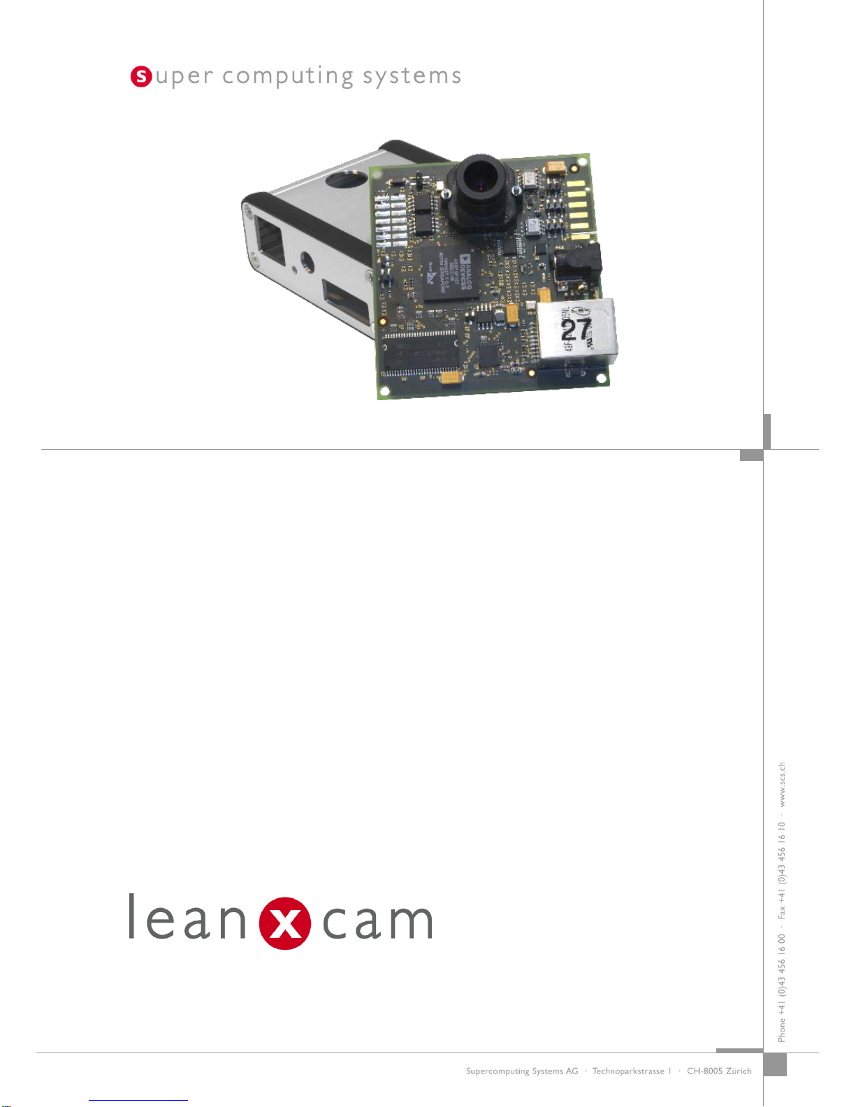
leanXcam is an intelligent colour camera with a rich set of features that provides an impressive
performance, in spite of its low production cost. The smart combination of a well-established sensor
chip, a fast digital signal processor, a tailored Linux-based operation system and the image processing
framework from SCS-Vision makes the leanXcam an incomparable achievement in the field of Vision.
Communication is ensured by Ethernet connection and digital I/Os.
1.2 Purpose of this document
This document gives an overview of the leanXcam HW and provides information about the used
devices, interfaces and some examples. This document should be used by readers who are interested
in the physical blocks contained in the leanXcam or by readers who want to use more debug features
like RS232 and JTAG, when designing with the leanXcam.
Page 7

28. Juni 2012
7
Page 8
28. Juni 2012
8
2 Hardware Overview
This section gives an overview of the main components/devices and interfaces available on the
leanXcam board.
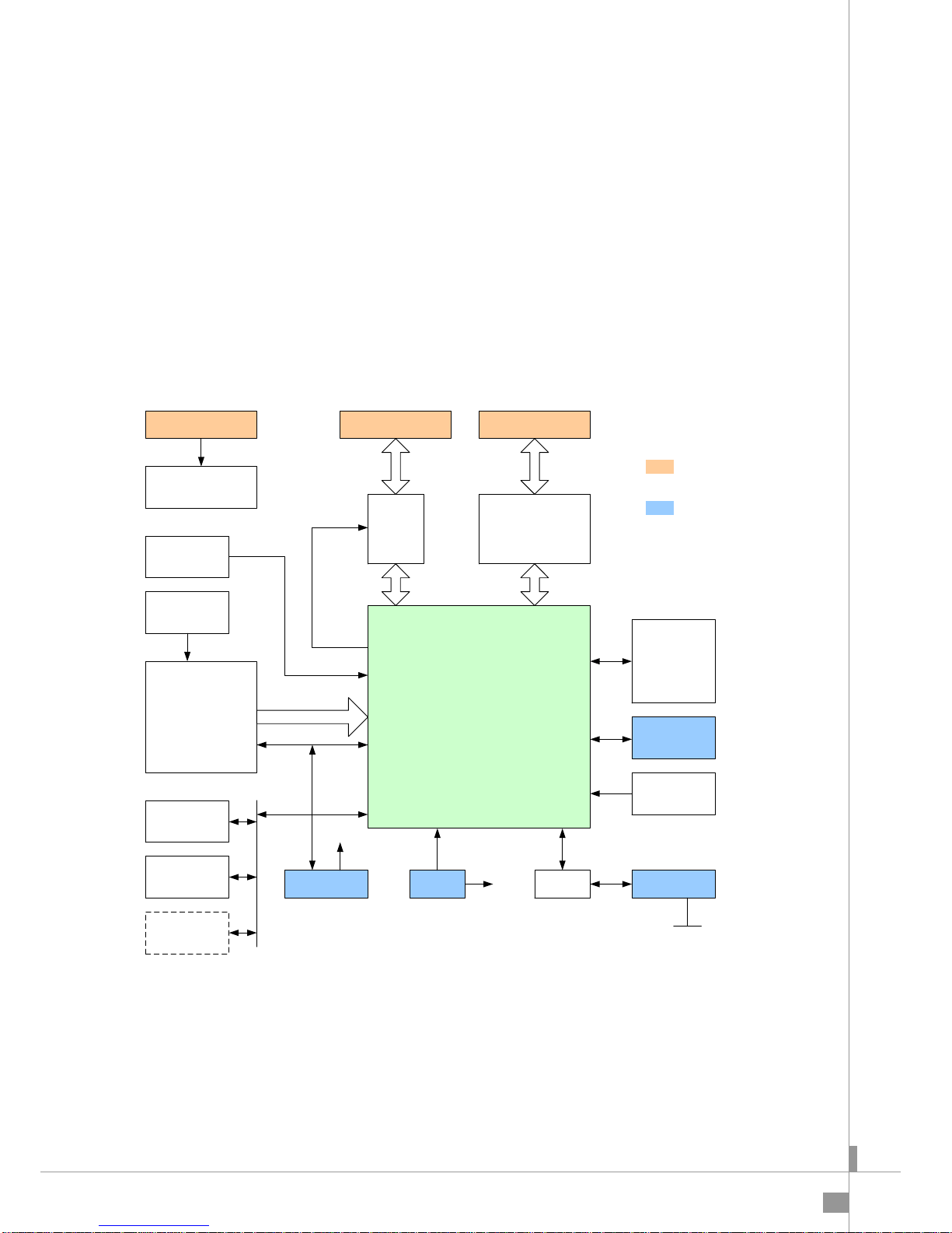
2.1 Block Diagram
In Figure 1 the block diagram of the leanXcam HW is shown.
CMOS Image
Sensor
Micron MT9V032
DSP
BlackFin ADSP-BF537
PPI
4 MByte
FLASH
4 MByte
FLASH
SPI
Systemclock
25MHz
Ethernet
PHY
EMAC
Clock_Out
Reset
I2C
sync.
Bus
SDRAM
64 MByte
Digital I/O
2 opt.inputs
2 opt. outputs
RS232
Reset UART0
Power Supply
5V -> 3.3V
JTAG
Real Time
Clock
Sensor Clock
26.6MHz
Eth_Clock
Clock_In
JTAG
Connector
3-pin header
GPIO
RJ45 Connector I/O Connector
3-pin header
I
2
C
optional
microSD slot
Vcc3.3
Legend:
Main Interfaces
User accessible through
socket connectors or
jumpers
Power Connector
Figure 1: Block Diagram
Page 9

28. Juni 2012
9
2.2 On-Board Devices
The leanXcam board offers the following devices:
- 500 MHz Digital Signal Processor Blackfin ADSP-BF537
- CMOS Sensor Micron MT9V032C12STC (color) or MT9V032C12STM (monochrome), Wide-
VGA 752H x 480V, 10Bit
- 64 MByte RAM Memory
- 4 MByte Flash for Boot program
- 4 MB Flash Memory for Algorithm Software
- microSD Card holder for optional Flash Memory expansion
- Voltage Regulator (LDO) for clean and stable 3.3V Supply Voltage
- Lens holder for standard M12x0.5 mount Lenses
2.3 Interfaces
The leanXcam Board supports the following interfaces:
- Fast-Ethernet 100Mb (10/100Mb) (RJ-45 Connector)
- RS232C Interface for first-time configuration during manufacturing (on-board header)
- I2C Interface to connect additional serial devices (on-board header)
- JTAG for Debugging DSP (on-board 14-pin 2-row header)
- 5V Power Input (6.5mm round connector Lumberg 1613 14)
- 2 optical isolated inputs and 2 optical isolated outputs (isolation can be jumpered, 1 input can
be used as external exposure, 1 output can be used for external flash triggering) with a 6-pin
Phoenix direct-PCB connector. Also see Figure 2 and Figure 3 for details
- Power-ON LED (on-board)
- Link speed und Link activity LED (in RJ45 connector, external view)
- Bi-color status LED (external view)
Page 10

28. Juni 2012
10
2.3.1 Digital Inputs, optically isolated
68R
to DSP
Input 145
68R
to DSP
Input 2 6
1
VIN
external Supply
I/O GND
Jumper J602
Fairchild
MOCD207R2M
Fairchild
MOCD207R2M
Figure 2: Digital Inputs
Jumper 602 can be used to connect the Ground to the I/O GND, if isolation is not required.
Page 11

28. Juni 2012
11
2.3.2 Digital Outputs, optically isolated
Output 1from DSP
from DSP Output 2
Jumper J602
I/O GND
2
3
4
1 external Supply
VIN
Fairchild
MOCD207R2M
Fairchild
MOCD207R2M
33R
33R
Figure 3: Digital Outputs
Jumper 602 can be used to connect the Ground to the I/O GND, if isolation is not required.
Page 12

28. Juni 2012
12
3 Hardware Components
3.1 Main Components
The main components of the leanXcam are as follows:
Data Flash CMOS Sensor Optocoupler I/O Connector
Program Flash Blackfin DSP RS232 Driver LDO Power Connector
SDRAM FET (VR) for DSP Ethernet Physical Ethernet Connector
Page 13

28. Juni 2012
13
3.2 LED Indicators
The leanXcam has two LED indicators, one power LED and one bi-color status LED:
Power LED (3.3V)
Status LED (red / green), software-controllable
Page 14

28. Juni 2012
14
3.3 Quartz and Clock Oscillators
The leanXcam has two clock oscillators and one Quartz:
26.66 MHz Oscillator for CMOS sensor (arrow points to clock pin)
32.768 kHz Quartz for RTC
25 MHz Main clock oscillator for DSP and Ethernet (arrow points to clock pin)
Page 15

28. Juni 2012
15
3.4 Supply Measurement Points
There are on-board voltages which can be measured at the following points:
3.3 Volt VIN (5 Volt)
Ground
Page 16

28. Juni 2012
16
3.5 On-Board Headers and Jumpers
The leanXcam has the following headers and jumpers:
Boot Jumper Factory Reset Jumper RS232C Interface Header I/O GND to GND Jumper
JTAG Connector (not populated) I2C Interface Header
Note: Arrows point to Pin 1 of the headers
Page 17

28. Juni 2012
17
3.5.1 Pinout of the On-Board Headers
Boot Jumper J202
Selection
Description
No Jumper
DSP boots from on-board Flash chip (default)
Jumper inserted
DSP boots from RS232C interface
I/O GND to GND Jumper J602
Selection
Description
No Jumper
inputs and outputs of connector J601 are isolated
Jumper inserted
I/O GND of J601 is connected to System GND (inputs and outputs are
NOT isolated)
Factory Reset Jumper J302
Selection
Description
No Jumper
normal operation (default)
Jumper inserted
Resets the factory default IP address 192.168.1.1 on power-up,
remove this jumper when the leanXcam is accessible afterwards
RS232C Header J702
Pin Number
I/O
Description
1
Input
UART Receive input pin, RS232 level (input to leanXcam)
2
Output
UART Transmit output pin, RS232 level (output from leanXcam)
3
Power
System Ground
Page 18

28. Juni 2012
18
I2C Header J401
Pin Number
I/O
Description
1
Power
3.3V Supply (without fuse !)
2
I/O
SCL Signal (I2C Clock)
3
I/O
SDA Signal (I2C Data)
Page 19

28. Juni 2012
19
3.6 Interface Connectors
The external connectors of the leanXcam are as follows:
5V Power Input Connector (+ at Center) I/O Connector
optional microSD Card connector (backside) Pin 1 Pin 6
Ethernet Connector (RJ45)
Page 20

28. Juni 2012
20
3.6.1 Pinout of the I/O Connector
Connector J601 (Phoenix Contact No: ZEC1,0/6-ST-3,5C1R1)
Pin Number
I/O
Description
1
Power
VIN 5 Volt (connected to the power connector without fuse)
default: leave unconnected or use as power for external devices
(max. 100mA)
2
Output
Output 1 (connected through a 33R current-limit-resistor to the
collector of the opto-coupler output transistor)
3
Output
Output 2 (connected through a 33R current-limit-resistor to the
collector of the opto-coupler output transistor)
This output can be used as a trigger for an external flash
4
Power
I/O Ground (can be connected to System Ground with the Jumper
J602
5
Input
Input 1 (connected through a 68R current-limit-resistor to the anode of
the opto-coupler LED)
6
Input
Input 2 (connected through a 68R current-limit-resistor to the anode of
the opto-coupler LED)
This input can be used as an external exposure trigger
Page 21

28. Juni 2012
21
4 Mechanical Dimension
4.1 Mechanical Dimensions of the PCB
Figure 4: PCB dimensions
Page 22

28. Juni 2012
22
4.2 Mechanical Dimensions of the enclosure
Figure 5: enclosure dimensions
Page 23

28. Juni 2012
23
5 Examples
In this section some examples of typical digital IO Interface connections are shown. Connect the
external devices and logic like shown in these examples, if this is appropriate for the current design
and use.
5.1 External Flash Circuit Example
1k
4k7
Flash Trigger
Signal (3.3V)
NPN Transistor
for ex. 12V
LED Array
Figure 6:LED Flash Example
Page 24

28. Juni 2012
24
5.2 Simple Output Example
from DSP
from DSP
Jumper J602
2
3
4
1
VIN
Fairchild
MOCD207R2M
Fairchild
MOCD207R2M
33R
33R 220R
220R
Figure 7: Non-isolated Output
Page 25

28. Juni 2012
25
5.3 Isolated Output Example
from DSP
from DSP
Jumper J602
2
3
4
1
VIN
Fairchild
MOCD207R2M
Fairchild
MOCD207R2M
33R
33R
1k1k
12 Volt
Figure 8: Isolated output example
 Loading...